EP2858131A2 - Light emitting device package - Google Patents
Light emitting device package Download PDFInfo
- Publication number
- EP2858131A2 EP2858131A2 EP14179994.0A EP14179994A EP2858131A2 EP 2858131 A2 EP2858131 A2 EP 2858131A2 EP 14179994 A EP14179994 A EP 14179994A EP 2858131 A2 EP2858131 A2 EP 2858131A2
- Authority
- EP
- European Patent Office
- Prior art keywords
- light emitting
- emitting device
- chip
- disposed
- package body
- Prior art date
- Legal status (The legal status is an assumption and is not a legal conclusion. Google has not performed a legal analysis and makes no representation as to the accuracy of the status listed.)
- Granted
Links
Images






Classifications
-
- H—ELECTRICITY
- H10—SEMICONDUCTOR DEVICES; ELECTRIC SOLID-STATE DEVICES NOT OTHERWISE PROVIDED FOR
- H10H—INORGANIC LIGHT-EMITTING SEMICONDUCTOR DEVICES HAVING POTENTIAL BARRIERS
- H10H20/00—Individual inorganic light-emitting semiconductor devices having potential barriers, e.g. light-emitting diodes [LED]
- H10H20/80—Constructional details
- H10H20/85—Packages
-
- F—MECHANICAL ENGINEERING; LIGHTING; HEATING; WEAPONS; BLASTING
- F21—LIGHTING
- F21V—FUNCTIONAL FEATURES OR DETAILS OF LIGHTING DEVICES OR SYSTEMS THEREOF; STRUCTURAL COMBINATIONS OF LIGHTING DEVICES WITH OTHER ARTICLES, NOT OTHERWISE PROVIDED FOR
- F21V29/00—Protecting lighting devices from thermal damage; Cooling or heating arrangements specially adapted for lighting devices or systems
- F21V29/50—Cooling arrangements
- F21V29/70—Cooling arrangements characterised by passive heat-dissipating elements, e.g. heat-sinks
-
- F—MECHANICAL ENGINEERING; LIGHTING; HEATING; WEAPONS; BLASTING
- F21—LIGHTING
- F21V—FUNCTIONAL FEATURES OR DETAILS OF LIGHTING DEVICES OR SYSTEMS THEREOF; STRUCTURAL COMBINATIONS OF LIGHTING DEVICES WITH OTHER ARTICLES, NOT OTHERWISE PROVIDED FOR
- F21V3/00—Globes; Bowls; Cover glasses
-
- F—MECHANICAL ENGINEERING; LIGHTING; HEATING; WEAPONS; BLASTING
- F21—LIGHTING
- F21V—FUNCTIONAL FEATURES OR DETAILS OF LIGHTING DEVICES OR SYSTEMS THEREOF; STRUCTURAL COMBINATIONS OF LIGHTING DEVICES WITH OTHER ARTICLES, NOT OTHERWISE PROVIDED FOR
- F21V3/00—Globes; Bowls; Cover glasses
- F21V3/04—Globes; Bowls; Cover glasses characterised by materials, surface treatments or coatings
- F21V3/10—Globes; Bowls; Cover glasses characterised by materials, surface treatments or coatings characterised by coatings
-
- H—ELECTRICITY
- H10—SEMICONDUCTOR DEVICES; ELECTRIC SOLID-STATE DEVICES NOT OTHERWISE PROVIDED FOR
- H10H—INORGANIC LIGHT-EMITTING SEMICONDUCTOR DEVICES HAVING POTENTIAL BARRIERS
- H10H20/00—Individual inorganic light-emitting semiconductor devices having potential barriers, e.g. light-emitting diodes [LED]
- H10H20/80—Constructional details
- H10H20/85—Packages
- H10H20/8506—Containers
-
- H—ELECTRICITY
- H10—SEMICONDUCTOR DEVICES; ELECTRIC SOLID-STATE DEVICES NOT OTHERWISE PROVIDED FOR
- H10H—INORGANIC LIGHT-EMITTING SEMICONDUCTOR DEVICES HAVING POTENTIAL BARRIERS
- H10H20/00—Individual inorganic light-emitting semiconductor devices having potential barriers, e.g. light-emitting diodes [LED]
- H10H20/80—Constructional details
- H10H20/85—Packages
- H10H20/852—Encapsulations
- H10H20/853—Encapsulations characterised by their shape
-
- F—MECHANICAL ENGINEERING; LIGHTING; HEATING; WEAPONS; BLASTING
- F21—LIGHTING
- F21Y—INDEXING SCHEME ASSOCIATED WITH SUBCLASSES F21K, F21L, F21S and F21V, RELATING TO THE FORM OR THE KIND OF THE LIGHT SOURCES OR OF THE COLOUR OF THE LIGHT EMITTED
- F21Y2115/00—Light-generating elements of semiconductor light sources
- F21Y2115/10—Light-emitting diodes [LED]
-
- H—ELECTRICITY
- H10—SEMICONDUCTOR DEVICES; ELECTRIC SOLID-STATE DEVICES NOT OTHERWISE PROVIDED FOR
- H10H—INORGANIC LIGHT-EMITTING SEMICONDUCTOR DEVICES HAVING POTENTIAL BARRIERS
- H10H20/00—Individual inorganic light-emitting semiconductor devices having potential barriers, e.g. light-emitting diodes [LED]
- H10H20/80—Constructional details
- H10H20/85—Packages
- H10H20/857—Interconnections, e.g. lead-frames, bond wires or solder balls
-
- H—ELECTRICITY
- H10—SEMICONDUCTOR DEVICES; ELECTRIC SOLID-STATE DEVICES NOT OTHERWISE PROVIDED FOR
- H10W—GENERIC PACKAGES, INTERCONNECTIONS, CONNECTORS OR OTHER CONSTRUCTIONAL DETAILS OF DEVICES COVERED BY CLASS H10
- H10W72/00—Interconnections or connectors in packages
- H10W72/071—Connecting or disconnecting
- H10W72/075—Connecting or disconnecting of bond wires
- H10W72/07551—Connecting or disconnecting of bond wires characterised by changes in properties of the bond wires during the connecting
- H10W72/07554—Connecting or disconnecting of bond wires characterised by changes in properties of the bond wires during the connecting changes in dispositions
-
- H—ELECTRICITY
- H10—SEMICONDUCTOR DEVICES; ELECTRIC SOLID-STATE DEVICES NOT OTHERWISE PROVIDED FOR
- H10W—GENERIC PACKAGES, INTERCONNECTIONS, CONNECTORS OR OTHER CONSTRUCTIONAL DETAILS OF DEVICES COVERED BY CLASS H10
- H10W72/00—Interconnections or connectors in packages
- H10W72/50—Bond wires
- H10W72/541—Dispositions of bond wires
- H10W72/547—Dispositions of multiple bond wires
-
- H—ELECTRICITY
- H10—SEMICONDUCTOR DEVICES; ELECTRIC SOLID-STATE DEVICES NOT OTHERWISE PROVIDED FOR
- H10W—GENERIC PACKAGES, INTERCONNECTIONS, CONNECTORS OR OTHER CONSTRUCTIONAL DETAILS OF DEVICES COVERED BY CLASS H10
- H10W72/00—Interconnections or connectors in packages
- H10W72/851—Dispositions of multiple connectors or interconnections
- H10W72/874—On different surfaces
- H10W72/884—Die-attach connectors and bond wires
-
- H—ELECTRICITY
- H10—SEMICONDUCTOR DEVICES; ELECTRIC SOLID-STATE DEVICES NOT OTHERWISE PROVIDED FOR
- H10W—GENERIC PACKAGES, INTERCONNECTIONS, CONNECTORS OR OTHER CONSTRUCTIONAL DETAILS OF DEVICES COVERED BY CLASS H10
- H10W90/00—Package configurations
- H10W90/701—Package configurations characterised by the relative positions of pads or connectors relative to package parts
- H10W90/751—Package configurations characterised by the relative positions of pads or connectors relative to package parts of bond wires
- H10W90/756—Package configurations characterised by the relative positions of pads or connectors relative to package parts of bond wires between a chip and a stacked lead frame, conducting package substrate or heat sink
Definitions
- Such a light emitting diode does not contain environmentally harmful substances such as mercury (Hg) used in conventional lighting apparatuses such as incandescent lamps or fluorescent lamps and thus advantageously has superior eco-friendliness, long lifespan and low power consumption, thus being used as alternatives of conventional light sources.
- Hg mercury
- the molding part 60 may be broken.
- the molding member may be disposed to extend up to an inside edge of the at least one molding groove.
- the at least one molding groove may have a circular planar shape.
- the molding member is disposed to extend up to an outer edge of the at least one molding groove.
- the molding member may have a viscosity of less than 3,000 mPa*sec in liquid form prior to hardening.
- the light emitting device chip 130 and the submount 140 are disposed on the first body 110A of the package body 110.
- the light emitting device chip 130 and the submount 140 may be disposed on the second body 110B of the package body 110 unlike FIGs. 2 to 4 . Even in this case, the following description will be equally applied.
- a portion of the second central segment CA2 in which the light emitting device chip 130 and the submount 140 are disposed corresponds to a chip mount area CMA and a portion of the second central segment CA2 excluding the chip mount area CMA corresponds to a chip non-mount area.
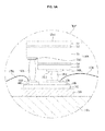
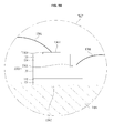
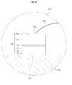
- FIGs. 5A to 5C are enlarged sectional views showing embodiments K1, K2, and K3 of a portion 'K' of FIG. 4 .
- Reference symbols 130A, 130B, and 130C correspond to embodiments of the light emitting device chip 130 of FIG. 4 .
- the support 137 may be formed of a material selected from a group consisting of molybdenum (Mo), silicon (Si), tungsten (W), copper(Cu), and aluminum (Al) or an alloy thereof.
- the support 137 may selectively include at least one of gold (Au), copper alloy (Cu Alloy), nickel (Ni), copper-tungsten (Cu-W), or a carrier wafer (e.g. at least one of GaN, Si, Ge, GaAs, ZnO, SiGe, SiC, SiGe, or Ga 2 O 3 ).
- the reflective layer 138 serves to reflect light emitted from the active layer 134 upward.
- the reflective layer 138 is disposed on the support 137.
- the reflective layer 138 may have a thickness of about 2500 ⁇ .
- the reflective layer 138 may be formed of a metal layer including aluminum (Al), silver (Ag), nickel (Ni), platinum (Pt), rhodium (Rh), or an alloy including at least one of Al, Ag, Pt, or Rh.
- Aluminum or silver may effectively reflect light generated from the active layer 134, thereby greatly improving light extraction efficiency of the light emitting device.
- an upper surface 130-1 of the light emitting device chip 130 is higher than an upper surface 111A of the package body 110 in the chip non-mount area of the central area CA and than an upper surface 111 B of the package body 110 in the peripheral area PA1 and PA2.
- a lower surface 130-2 of the light emitting device chip 130 is higher than the upper surface 111A of the package body 110 in the chip non-mount area of the central area CA and than the upper surface 111 B of the package body 110 in the peripheral area PA1 and PA2.
- the molding member 60 has a first height h 1 ranging from 0 to 0.1d 1 on the basis of the uppermost surface of the cavity in the conventional light emitting device packages as shown in FIG. 1 .
- 'd 1 ' means the width of the molding member 60 positioned over the uppermost surface of the package body 10.
- the molding member 150A has a second height h 2 ranging from 0.15d 2 to 0.35d 2 on the basis of the uppermost surface 111 B of the package body 110.
- 'd 2 ' means the width of the molding member 150A positioned over the uppermost surface 111 B of the package body 110 and is subsequently equal to the width of the central area CA.
- the radius of curvature of the molding member 150A of the light emitting device package 100A according to the embodiment shown in FIGs. 2 to 4 becomes smaller than that of the molding part 60 of the conventional light emitting device package shown in FIG. 1 . That is, it can be seen that the molding member 150A has a more convex shape than the molding part 60. Consequently, light extraction efficiency of the light emitting device package 100A according to the embodiment may be improved by the provision of the at least one molding groove 114.
- the light emitting device packages 100A and 100B shown in FIGs. 4 and 8 each have a molding groove 114, whereas the light emitting device package 100C shown in FIG. 9 has a dam 190A. Except the above difference, the light emitting device package 100C shown in FIG. 9 is identical to the light emitting device package 100A shown in FIG. 4 . Consequently, the same reference symbols are used and a repeated description thereof will be omitted.
- the light emitting device package 100D shown in FIG. 10 further has a first cavity 180 in a central area CA. Except this difference, the light emitting device package 100D shown in FIG. 10 is identical to the light emitting device package 100C shown in FIG. 9 . Consequently, the same reference symbols are used and a repeated description thereof will be omitted.
- the first cavity 180 shown in FIG. 10 is identical to the first cavity 180 shown in FIG. 8 and, therefore, a detailed description thereof will be omitted. That is, the light emitting device package 100D shown in FIG. 10 has a second cavity 182 in addition to the first cavity 180 unlike the light emitting device package 100B or 100C shown in FIG. 8 or 9 .
- the board 512 is disposed along the inside of the casing 510 in a single line.
- the board 512 may be a printed circuit board (PCB) including a circuit pattern (not shown).
- the board 512 may include a metal core PCB (MCPCB) and a flexible PCB in addition to a general PCB.
- MCPCB metal core PCB
- embodiments are not limited thereto.
- the power connection unit 540 may be formed in a flat shape.
- the power connection unit 540 may be formed in the shape of a socket or a cable slot to which an external power cable (not shown) may be electrically connected.
- the power cable may be flexible such that the power cable is easily connected to the external power.
- the head lamp 900 includes a light emitting module 901, a reflector 902, a shade 903, and a lens 904.
- Light emitted from the light emitting module 901 is reflected by the reflector 902 and the shade 903, is transmitted through the lens 904, and is directed to the front of a vehicle.
- the lens 904 may refract the light reflected by the reflector 902 to the front.
- the light source module 1200 may include the light emitting device packages 100A to 100E shown in FIGs. 2 to 4 and 8 to 11 or the light emitting device chips 130A to 130C shown in FIGs. 5A to 5C .
- the holder 1500 blocks a reception groove 1719 of an insulative part 1710 of the inner case 1700. Consequently, the power supply 1600 received in the insulative part 1710 of the inner case 1700 may be hermetically sealed.
- the holder 1500 may have a guide protrusion 1510.
- the guide protrusion 1510 may have a hole through which a protrusion 1610 of the power supply 1600 passes.
Landscapes
- Engineering & Computer Science (AREA)
- General Engineering & Computer Science (AREA)
- Led Device Packages (AREA)
- Microelectronics & Electronic Packaging (AREA)
Abstract
Description
- Embodiments relate to a light emitting device package.
- Light emitting diodes (LEDs) are semiconductor devices which send and receive a signal by converting electricity into infrared light or visible light using characteristics of compound semiconductors or are used as light sources.
- Group III-V nitride semiconductors receive much attention as essential materials for light emitting devices such as light emitting diodes (LEDs) or laser diodes (LDs) due to physical and chemical properties thereof.
- Such a light emitting diode does not contain environmentally harmful substances such as mercury (Hg) used in conventional lighting apparatuses such as incandescent lamps or fluorescent lamps and thus advantageously has superior eco-friendliness, long lifespan and low power consumption, thus being used as alternatives of conventional light sources.
-
FIG. 1 is a sectional view showing a conventional light emitting device package. - Referring to
FIG. 1 , the conventional light emitting device package includespackage bodies insulative material 20, a lightemitting device chip 30, a submount 40,wires - The
package bodies emitting device chip 30 is disposed on thepackage body 10A in the cavity. In a case in which the lightemitting device chip 30 is disposed in the cavity as described above, a portion of light emitted from the lightemitting device chip 30 is captured in the cavity, whereby an amount of light is reduced. - Furthermore, when high current of, for example, 20 mA is supplied to the light
emitting device chip 30, the molding part 60 may be broken. - In addition, since the light
emitting device chip 30 is captured in the cavity, light exits only in a vertical direction 5. As a result, it is difficult to satisfy various demands of consumers. - Embodiments provide a light emitting device package in which light extraction efficiency is improved, a molding member is prevented from being broken, and light exits in all directions.
- In one embodiment, a light emitting device package may include a package body; a light emitting device chip disposed on a chip mount area of the package body; and a molding member disposed on the package body, wherein the package body comprises: a central area having the chip mount area and a chip non-mount area adjacent to the chip mount area, the molding member being disposed on the central area; and a peripheral area around the central area, and wherein an upper surface of the light emitting device chip is higher than an upper surface of the package body in the chip non-mount area and than an upper surface of the package body in the peripheral area.
- A lower surface of the light emitting device chip may be higher than the upper surface of the package body in the chip non-mount area and than the upper surface of the package body in the peripheral area.
- The central area may include a first cavity in which the light emitting device chip is disposed.
- The molding member may be disposed to surround the light emitting device chip, and the package body may include at least one molding groove defining a boundary of the molding member.
- The at least one molding groove may be disposed in the peripheral area on the package body at an interface between the peripheral area and the central area.
- The molding member may be disposed to extend up to an inside edge of the at least one molding groove.
- The at least one molding groove may have a circular planar shape.
- The molding member is disposed to extend up to an outer edge of the at least one molding groove.
- The molding member does not extend beyond an edge of the at least one molding groove.
- The light emitting device package may further include a dam disposed on the peripheral area on the package body at an interface between the peripheral area and the central area, the dam defining a second cavity.
- A top surface of the dam may be higher than the upper surface of the light emitting device chip.
- The dam may include transparent material.
- A top surface of the dam may be lower than the upper surface of the light emitting device chip.
- The top surface of the dam may be lower than a lower surface of the light emitting device chip.
- The molding member may be disposed to extend up to an inner wall of the dam while filling the second cavity.
- The molding member may be put on the dam for covering the second cavity.
- The molding member may be coupled to the dam by eutectic bonding.
- The second cavity may be under vacuum.
- The molding member may have a viscosity of less than 3,000 mPa*sec in liquid form prior to hardening.
- In another embodiment, a lighting apparatus may include a light source module including a light emitting device package; and a cover optically coupled to the light source module, wherein the light emitting device package may include a package body; a light emitting device chip disposed on a chip mount area of the package body; and a molding member disposed on the package body, wherein the package body may include a central area having the chip mount area and a chip non-mount area adjacent to the chip mount area, the molding member being disposed on the central area; and a peripheral area around the central area, and wherein an upper surface of the light emitting device chip is higher than an upper surface of the package body in the chip non-mount area and than an upper surface of the package body in the peripheral area.
- Arrangements and embodiments may be described in detail with reference to the following drawings in which like reference numerals refer to like elements and wherein:
-
FIG. 1 is a sectional view showing a conventional light emitting device package; -
FIG. 2 is a perspective view showing a light emitting device package according to an embodiment; -
FIG. 3 is a plan view of the light emitting device package shown inFIG. 2 ; -
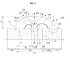
FIG. 4 is a sectional view taken along line A-A' ofFIG. 3 ; -
FIGs. 5A to 5C are enlarged sectional views showing embodiments of portion 'K' ofFIG. 4 ; -
FIG. 6 is an enlarged partial sectional view showing a portion 'L' ofFIG. 4 ; -
FIGs. 7A and 7B are views illustrating a radius of curvature of a molding member; -
FIG. 8 is a sectional view showing a light emitting device package according to another embodiment; -
FIG. 9 is a sectional view showing a light emitting device package according to still another embodiment; -
FIG. 10 is a sectional view showing a light emitting device package according to still another embodiment; -
FIG. 11 is a sectional view showing a light emitting device package according to still another embodiment; -
FIG. 12 is a perspective view showing an air sterilization apparatus including light emitting device packages according to an embodiment; -
FIG. 13 is a view showing a head lamp including light emitting device packages according to an embodiment; and -
FIG. 14 is a view showing a lighting apparatus including light emitting device packages according to an embodiment. - Hereinafter, embodiments will be described with reference to the accompanying drawings. However, embodiments may be modified into various other forms. Embodiments are not restrictive but are illustrative. Embodiments are provided to more completely explain the disclosure to a person having ordinary skill in the art.
- It will be understood that when an element is referred to as being 'on' or 'under' another element, it can be directly on/under the element, and one or more intervening elements may also be present. When an element is referred to as being 'on' or 'under', 'under the element' as well as 'on the element' can be included based on the element.
- Meanwhile, relational terms, such as 'first' and 'second' and 'upper part' and 'lower part', are used only to distinguish between one subject or element and another subject and element without necessarily requiring or involving any physical or logical relationship or sequence between such subjects or elements.
- In the drawings, the thicknesses or sizes of respective layers are exaggerated, omitted, or schematically illustrated for convenience and clarity of description. Further, the sizes of the respective elements do not denote the actual sizes thereof.
-
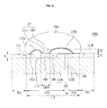
FIG. 2 is a perspective view showing a lightemitting device package 100A according to an embodiment,FIG. 3 is a plan view of the lightemitting device package 100A shown inFIG. 2 , andFIG. 4 is a sectional view taken along line A-A' ofFIG. 3 . For the convenience of description, aninsulation part 120 is omitted fromFIG. 2 and amolding member 150A is omitted fromFIG. 3 . - Referring to
FIGs. 2 to 4 , the light emittingdevice package 100A includes apackage body 110, aninsulation part 120, a light emittingdevice chip 130, asubmount 140, amolding member 150A, andwires - The
package body 110 includes afirst body 110A and asecond body 110B, which are electrically separated from each other by theinsulation part 120. - In addition, the
package body 110 may be divided into a central area CA and a peripheral area PA1 and PA2. - The central area CA is defined as an area in which the light emitting
device chip 130 and themolding member 150A are disposed. The central area CA may be divided into a first central segment CA1, a second central segment CA2, and an insulation segment IA. The first central segment CA1 corresponds to a portion of the central area CA in which thefirst body 110A is disposed. The second central segment CA2 corresponds to a portion of the central area CA in which thesecond body 110B is disposed. The insulation segment IA corresponds to a portion of the central area CA in which theinsulation part 120 is disposed. - The first or second central segment CA1 or CA2 may be divided into a chip mount area CMA and a chip non-mount area, which are adjacent to each other. Referring to
FIG. 4 , there is shown a chip mount area CMA of the first central segment CA1 in which the light emittingdevice chip 130 is mounted. A portion of the first central segment CA1 excluding the chip mount area CMA corresponds to a chip non-mount area. In a case in which the light emittingdevice chip 130 has a flip-chip bonding structure as shown inFIGs. 2 to 4 , an area in which thesubmount 140 is disposed corresponds to the chip mount area CMA. - In
FIGs. 2 to 4 , the light emittingdevice chip 130 and thesubmount 140 are disposed on thefirst body 110A of thepackage body 110. However, embodiments are not limited thereto. According to another embodiment, the light emittingdevice chip 130 and thesubmount 140 may be disposed on thesecond body 110B of thepackage body 110 unlikeFIGs. 2 to 4 . Even in this case, the following description will be equally applied. In this case, a portion of the second central segment CA2 in which the light emittingdevice chip 130 and thesubmount 140 are disposed corresponds to a chip mount area CMA and a portion of the second central segment CA2 excluding the chip mount area CMA corresponds to a chip non-mount area. - Meanwhile, the peripheral area is an area around the central area CA. The peripheral area is defined as including a periphery of the
package body 110. The peripheral area may be divided into first and second peripheral segments PA1 and PA2. The first peripheral segment PA1 corresponds to a portion of thefirst body 110A excluding the first central segment CA1 and the second peripheral segment PA2 corresponds to a portion of thesecond body 110B excluding the second central segment CA2. - The
package body 110 may be formed of ceramic or metal. In a case which the light emittingdevice chip 130 emits ultraviolet (UV)-wavelength light, specifically deep UV-wavelength light, thepackage body 110 may be formed of aluminum (Al) for increasing reflectance and improving heat dissipation characteristics. - Meanwhile, referring to
FIGs. 2 to 4 , the light emittingdevice chip 130 is disposed on thesubmount 140 and thesubmount 140 is mounted at the chip mount area CMA on thefirst body 110A of thepackage body 110. Thesubmount 140 is disposed between the light emittingdevice chip 130 and thefirst body 110A. In a case in which the light emittingdevice chip 130 has a horizontal or vertical type structure as will hereinafter be described, the light emittingdevice chip 130 is disposed on the chip mount area CMA of thefirst body 110A of thepackage body 110. - The light emitting
device chip 130 includes a light emitting diode (LED) using a plurality of compound semiconductor layers, e.g. group III-V compound semiconductor layers. The LED may be a color LED emitting blue light, green light, or red light, an ultraviolet (UV) LED, specifically deep UV (DUV) LED, or a non-polar LED. Light emitted from the LED may be realized using various semiconductors. However, embodiments are not limited thereto. -
FIGs. 5A to 5C are enlarged sectional views showing embodiments K1, K2, and K3 of a portion 'K' ofFIG. 4 .Reference symbols device chip 130 ofFIG. 4 . - Referring to
FIG. 5A , according to an embodiment, the light emittingdevice chip 130A includes asubstrate 131, abuffer layer 132, alight emitting structure second electrodes - The
substrate 131 may be transparent such that light emitted from theactive layer 134 exits through thesubstrate 131. For example, thesubstrate 131 may be formed of at least one selected from among sapphire (Al2O3), SiC, GaAs, GaN, ZnO, Si, GaP, InP, and Ge. However, embodiments are not limited thereto. In addition, thesubstrate 131 may have mechanical strength, by which the entirety of the nitride semiconductor is prevent from being bent while thesubstrate 131 is easily cut into individual chips through a scribing process and a breaking process. - The
buffer layer 132 is disposed between thesubstrate 131 and thelight emitting structure substrate 131 and thelight emitting structure buffer layer 132 may include AIN or an undoped nitride. However, embodiments are not limited thereto. Thebuffer layer 132 may be omitted depending upon type of thesubstrate 131 and thelight emitting structure - The light emitting structure is disposed under the
buffer layer 132. The light emitting structure may include a firstconductive semiconductor layer 133, anactive layer 134, and a secondconductive semiconductor layer 135, which are sequentially stacked. - The first
conductive semiconductor layer 133 is disposed between thebuffer layer 132 and theactive layer 134. The firstconductive semiconductor layer 133 may be formed of a compound semiconductor. The firstconductive semiconductor layer 133 may be formed of a group III-V or II-VI compound semiconductor, which may be doped with a first conductive dopant. For example, the firstconductive semiconductor layer 133 may be formed of at least one selected from among a semiconductor material having a formula of AlxInyGa(1-x-y)N (0≤x≤1, 0≤y≤1, 0≤x+y≤1), InAlGaN, AlGaAs, GaP, GaAs, GaAsP, and AlGaInP. In a case in which the firstconductive semiconductor layer 133 is an n-type semiconductor layer, the first conductive dopant may include an n-type dopant, such as Si, Ge, Sn, Se, or Te. The firstconductive semiconductor layer 133 may be a single-layer or a multi-layer. However, embodiments are not limited thereto. In a case in which the light emittingdevice chip 130A ofFIG. 5A is a UV, specifically deep UV, or non-polar light emitting device, the firstconductive semiconductor layer 133 may include at least one of InAlGaN or AlGaN. - The
active layer 134 is disposed between the firstconductive semiconductor layer 133 and the secondconductive semiconductor layer 135. Theactive layer 134 may include at least one selected from among a single well structure, a multi well structure, a single quantum well structure, and a multi quantum well (MQW) structure, a quantum dot structure, and a quantum wire structure. Theactive layer 134 may be formed to have at least one pair structure of a well layer and a barrier layer selected from among InGaN/GaN, InGaN/InGaN, GaN/AlGaN, InAlGaN/GaN, GaAs(InGaAs)/AlGaAs, and GaP(InGaP)/AlGaP using a group III-V compound semiconductor material. However, embodiments are not limited thereto. The well layer may be formed of a material having an energy band gap lower than that of the barrier layer. Particularly, in this embodiment, theactive layer 134 may generate UV-wavelength, specifically deep UV-wavelength, light. - The second
conductive semiconductor layer 135 may be disposed under theactive layer 134. The secondconductive semiconductor layer 135 may be formed of a compound semiconductor. The secondconductive semiconductor layer 135 may be formed of a group III-V or II-VI compound semiconductor, which may be doped with a second conductive dopant. For example, the secondconductive semiconductor layer 135 may be formed of at least one selected from among a semiconductor material having a formula of InxAlyGa1-x-yN (0≤x≤1, 0≤y≤1, 0≤x+y≤1), AlInN, AlGaAs, GaP, GaAs, GaAsP, and AlGaInP. In a case in which the secondconductive semiconductor layer 135 is a p-type semiconductor layer, the second conductive dopant may be a p-type dopant, such as Mg, Zn, Ca, Sr, or Ba. The secondconductive semiconductor layer 135 may be a single-layer or a multi-layer. However, embodiments are not limited thereto. In a case in which the light emittingdevice chip 130A is a UV (specifically, DUV) or non-polar light emitting device, the secondconductive semiconductor layer 135 may include at least one of InAlGaN or AlGaN. - The
first electrode 136A is disposed under the firstconductive semiconductor layer 133. For example, thefirst electrode 136A may include at least one of AIN or BN. However, embodiments are not limited thereto. That is, thefirst electrode 136A may be formed of any material that may not absorb but reflect or transmit light emitted from theactive layer 134 and may be grown on the firstconductive semiconductor layer 133 with high quality. - In addition, the
first electrode 136A may include an ohmic contact material such that thefirst electrode 136A can execute an ohmic function. In this case, it is not necessary to provide an additional ohmic layer (not shown). On the other hand, an additional ohmic layer may be disposed under thefirst electrode 136A. - The
second electrode 136B contacts the secondconductive semiconductor layer 135. Thesecond electrode 136B may be formed of metal. For example, thesecond electrode 136B may be formed of Ag, Ni, Al, Rh, Pd, Ir, Ru, Mg, Zn, Pt, Au, Hf, or a selective combination thereof. - The
second electrode 136B may be a transparent conductive oxide (TCO). For example, thesecond electrode 136B may include at least one selected from among the above-specified metal materials, indium tin oxide (ITO), indium zinc oxide (IZO), indium zinc tin oxide (IZTO), indium aluminum zinc oxide (IAZO), indium gallium zinc oxide (IGZO), indium gallium tin oxide (IGTO), aluminum zinc oxide (AZO), antimony tin oxide (ATO), gallium zinc oxide (GZO), IrOx, RuOx, RuOx/ITO, Ni/IrOx/Au, and Ni/IrOx/Au/ITO. However, embodiments are not limited thereto. Thesecond electrode 136B may include a material ohmic-contacting the secondconductive semiconductor layer 135. - In addition, the
second electrode 136B may be formed of a reflective electrode material exhibiting ohmic characteristics and may have a single-layer structure or a multi-layer structure. In a case in which thesecond electrode 136B executes an ohmic function, an additional ohmic layer (not shown) may not be formed. - Continuously referring to
FIG. 5A , the light emittingdevice package 100A may further include apassivation layer 142 disposed between the light emittingdevice chip 130A and thesubmount 140, first andsecond electrode pads second bumps - The first and
second electrodes device chip 130A having a flip-chip bonding structure shown inFIG. 5A are located on thesubmount 140 in a flip-chip bonding fashion. - The
submount 140 may be formed of a semiconductor substrate, such as AIN, BN, silicon carbide (SiC), GaN, GaAs, or Si. However, embodiments are not limited thereto. For example, thesubmount 140 may be formed of a semiconductor material exhibiting high thermal conductivity. In addition, a Zener diode type device for electrostatic discharge (ESD) prevention may be included in thesubmount 140. - The
first electrode 136A is connected to thefirst electrode pad 144A of thesubmount 140 via thefirst bump 146A and thesecond electrode 136B is connected to thesecond electrode pad 144B of thesubmount 140 via thesecond bump 146B. Thewires device chip 130A to thepackage body 110. That is, thefirst electrode pad 144A is connected to thefirst body 110A via thewire 170A and thesecond electrode pad 144B is connected to thesecond body 110B via thewire 170B. - Although not shown, a first upper bump metal layer (not shown) may be further disposed between the
first electrode 136A and thefirst bump 146A and a first lowerbump metal layer 143A may be further disposed between thefirst electrode pad 144A and thefirst bump 146A. The first upper bump metal layer and the first lowerbump metal layer 143A serve to indicate a position of thefirst bump 146A. Similarly, a second upper bump metal layer (not shown) may be further disposed between thesecond electrode 136B and thesecond bump 146B and a second lowerbump metal layer 143B may be further disposed between thesecond electrode pad 144B and thesecond bump 146B. The second upper bump metal layer and the second lowerbump metal layer 143B serve to indicate a position of thesecond bump 146B. - In a case in which the submount is formed of a material, such as Si, exhibiting electrical conductivity, a
passivation layer 142 may be further disposed between the first andsecond electrode pads submount 140 as shown inFIG. 5A . Thepassivation layer 142 may be formed of an insulative material. - In the light emitting
device package 100A shown inFIGs. 2 to 4 , the light emittingdevice chip 130 may have a configuration (130A) in which the light emittingdevice chip 130 is connected to thepackage body 110 to have a flip-chip bonding structure as shown inFIG. 5A . However, embodiments are not limited thereto. That is, according to other embodiments, the light emittingdevice chip 130 may have a configuration (130B) in which the light emittingdevice chip 130 is connected to thepackage body 110 to have a horizontal bonding structure as shown inFIG. 5B and a configuration (130C) in which the light emittingdevice chip 130 is connected to thepackage body 110 to have a vertical bonding structure as shown inFIG. 5C . In the horizontal and vertical bonding structures, thesubmount 140 is omitted. Particularly in the vertical bonding structure, the light emittingdevice chip 130 may be directly mounted on thepackage body 110 such that the light emittingdevice chip 130 is electrically connected to thefirst body 110A without thewire 170A. Details thereof will be described. - Since the light emitting
device chip 130A shown inFIGs. 2 ,3 ,4 , and5A has the flip-chip bonding structure, light emitted from theactive layer 134 exits through the firstconductive semiconductor layer 133, thebuffer layer 132, and thesubstrate 131. Consequently, the firstconductive semiconductor layer 133, thebuffer layer 132, and thesubstrate 131 may be formed of a transparent material. - On the other hand, since the light emitting
device chip 130B shown inFIG. 5B has the horizontal bonding structure, light emitted from theactive layer 134 exits through the secondconductive semiconductor layer 135 and thesecond electrode 136B. To this end, the secondconductive semiconductor layer 135 and thesecond electrode 136B shown inFIG. 5B may be formed of a transparent material and the firstconductive semiconductor layer 133, thebuffer layer 132, and thesubstrate 131 may be formed of a transparent or non-transparent material. In addition, since the light emittingdevice chip 130B shown inFIG. 5B has the horizontal bonding structure, not the flip-chip bonding structure, the first andsecond bumps second electrode pads passivation layer 142, thesubmount 140, the first lowerbump metal layer 143A, and the second lowerbump metal layer 143B are not needed. Except the above differences, the light emittingdevice chip 130B shown inFIG. 5B is identical to the light emittingdevice chip 130A shown inFIG. 5A . Consequently, the same reference symbols are used and a detailed description thereof will be omitted. - In addition, the light emitting
device chip 130C having the vertical bonding structure shown inFIG. 5C includes asupport 137, areflective layer 138, alight emitting structure first electrode 136A. - The
support 137 may include a conductive material or a nonconductive material. For example, thesupport 137 may be formed of at least one selected from among sapphire (Al2O3), GaN, SiC, ZnO, GaP, InP, Ga2O3, GaAs, and Si. However, embodiments are not limited thereto. In a case in which thesupport 137 is conductive, the entirety of thesupport 137 may serve as a p-type electrode together with thereflective layer 138. Consequently, thesupport 137 may be formed of a metal exhibiting high electrical conductivity. In addition, thesupport 137 may be formed of a metal exhibiting high thermal conductivity since it is necessary for thesupport 137 to sufficiently dissipate heat generated during operation of the light emitting device. - For example, the
support 137 may be formed of a material selected from a group consisting of molybdenum (Mo), silicon (Si), tungsten (W), copper(Cu), and aluminum (Al) or an alloy thereof. In addition, thesupport 137 may selectively include at least one of gold (Au), copper alloy (Cu Alloy), nickel (Ni), copper-tungsten (Cu-W), or a carrier wafer (e.g. at least one of GaN, Si, Ge, GaAs, ZnO, SiGe, SiC, SiGe, or Ga2O3). - The
reflective layer 138 serves to reflect light emitted from theactive layer 134 upward. Thereflective layer 138 is disposed on thesupport 137. Thereflective layer 138 may have a thickness of about 2500 Ǻ. For example, thereflective layer 138 may be formed of a metal layer including aluminum (Al), silver (Ag), nickel (Ni), platinum (Pt), rhodium (Rh), or an alloy including at least one of Al, Ag, Pt, or Rh. Aluminum or silver may effectively reflect light generated from theactive layer 134, thereby greatly improving light extraction efficiency of the light emitting device. - Referring to
FIG. 5C , light emitted from theactive layer 134 exits through the firstconductive semiconductor layer 133 and thefirst electrode 136A. To this end, the firstconductive semiconductor layer 133 and thefirst electrode 136A may be formed of a transparent material and the secondconductive semiconductor layer 135 may be formed of a transparent or non-transparent material. In addition, since the light emittingdevice chip 130C shown inFIG. 5C has the vertical bonding structure, not the flip-chip bonding structure, the first andsecond bumps second electrode pads passivation layer 142, thesubmount 140, the first lowerbump metal layer 143A, and the second lowerbump metal layer 143B are not needed. Except the above differences, the light emittingdevice chip 130C shown inFIG. 5C is identical to the light emittingdevice chip 130A shown inFIG. 5A . Consequently, the same reference symbols are used and a detailed description thereof will be omitted. - Meanwhile, referring to
FIGs. 2 to 5C , an upper surface 130-1 of the light emittingdevice chip 130 is higher than anupper surface 111A of thepackage body 110 in the chip non-mount area of the central area CA and than anupper surface 111 B of thepackage body 110 in the peripheral area PA1 and PA2. In addition, a lower surface 130-2 of the light emittingdevice chip 130 is higher than theupper surface 111A of thepackage body 110 in the chip non-mount area of the central area CA and than theupper surface 111 B of thepackage body 110 in the peripheral area PA1 and PA2. - The upper surface 130-1 of the light emitting
device chip 130A shown inFIG. 5A corresponds to the top surface of thesubstrate 131, the upper surface 130-1 of the light emittingdevice chip 130B shown inFIG. 5B corresponds to the top surface of thesecond electrode 136B, and the upper surface 130-1 of the light emittingdevice chip 130C shown inFIG. 5C corresponds to the top surface of thefirst electrode 136A. - In addition, the lower surface 130-2 of the light emitting
device chip 130A shown inFIG. 5A corresponds to the bottom surface of thesecond electrode 136B, the lower surface 130-2 of the light emittingdevice chip 130B shown inFIG. 5B corresponds to the bottom surface of thesubstrate 131, and the lower surface 130-2 of the light emittingdevice chip 130C shown inFIG. 5C corresponds to the bottom surface of thesupport 137. - In the conventional light emitting device package shown in
FIG. 1 , an upper surface 30-1 and a lower surface 30-2 of the light emittingdevice chip 30 is higher than anupper surface 11A of a central area of thepackage body 10 but is lower than an upper surface 11 B of a peripheral area of thepackage body 10. Consequently, light emitted from the light emittingdevice chip 30 may be captured in a cavity of thepackage body 10 with the result that the light may not escape from the light emitting device package. Furthermore, light emitted from the light emittingdevice chip 30 may not escape in all directions but may escape only in a vertical direction 5 of the light emitting device package. - On the other hand, light emitted from the light emitting
device chip 130 having the aforementioned structure as shown inFIGs. 2 to 4 escape from the light emitting device package without being captured in thepackage body 110. Consequently, light extraction efficiency may be improved by about 25 %. Furthermore, the light emittingdevice package 100A according to the embodiment may emit light not only in the vertical direction 5 but also in all directions 7 as indicated by arrows ofFIG. 4 . - Meanwhile, referring to
FIGs. 2 to 4 , themolding member 150A is disposed on thepackage body 110 while surrounding the light emittingdevice chip 130. In addition, themolding member 150A may include a fluorescent substance, which may change wavelength of light emitted from the light emittingdevice chip 130. - The
package body 110 according to the embodiment includes at least onemolding groove 114. The at least onemolding groove 114 is disposed in the peripheral area PA1 and PA2 on thepackage body 110 at an interface between the central area CA1 and CA2 and the peripheral area PA1 and PA2. -
FIG. 6 is an enlarged partial sectional view showing a portion 'L' ofFIG. 4 . - Referring to
FIG. 6 , themolding member 150A is disposed to extend up to aninside edge 114A (e.g. an interface between the central area CA2 and the peripheral area PA2) of the at least onemolding groove 114. -
FIGs. 7A and 7B are views illustrating a radius of curvature of themolding member 150A. - In a case in which the light emitting
device chip 130 emits DUV light having a wavelength band of 200 nm to 405 nm, a geltype molding member 150A having lower viscosity than in a case in which blue light is emitted as previously described is used. For example, in case that the light emittingdevice chip 130 emits blue light, themolding member 150A has the viscosity ranging from 3,000 mPa•sec to 30,000 mPa•sec at an initial liquid form prior to hardening. In contrast, in case that the light emittingdevice chip 130 emits light having the wavelength ranging from 200 nm to 405 nm, themolding member 150A may have the viscosity ranging from 0 to 3,000 mPa•sec at an initial liquid form prior to hardening. - In this case, as shown in
FIG. 7A , the low-viscosity molding member 150A may not have a convex hemispherical shape but a flattened hemispherical shape spread in a direction indicated by an arrow. In a case in which the radius of curvature of themolding member 150A is big as described above, light extraction efficiency of the light emitting device package is lowered. - In the light emitting
device package 100A according to the embodiment, on the other hand, the at least onemolding groove 114 is disposed at the peripheral area PA1 and PA2 on thepackage body 110. Even in a case in which the viscosity of themolding member 150A is low, therefore, the low-viscosity molding member 150A may have an inflated hemispherical shape or a dome shape since horizontally spreading thereof is suppressed by surface tension indicated by arrows as shown inFIG. 7B . Consequently, the radius of curvature of themolding member 150A is decreased, thereby improving light extraction efficiency of the light emittingdevice package 100A. - In case that the light emitting
device chip 30 emits light having a wavelength ranging from 430 nm to 485 nm, the molding member 60 has a first height h1 ranging from 0 to 0.1d1 on the basis of the uppermost surface of the cavity in the conventional light emitting device packages as shown inFIG. 1 . Here, 'd1' means the width of the molding member 60 positioned over the uppermost surface of thepackage body 10. Also, referring toFIG 4 , in case that the light emittingdevice chip 130 emits light having a wavelength ranging from 200 nm to 405 nm, themolding member 150A has a second height h2 ranging from 0.15d2 to 0.35d2 on the basis of theuppermost surface 111 B of thepackage body 110. Here, 'd2' means the width of themolding member 150A positioned over theuppermost surface 111 B of thepackage body 110 and is subsequently equal to the width of the central area CA. - Thus, since the at least one
molding groove 114 is disposed in the embodiment, the second height h2 of themolding member 150A may increase by from 0.05d to 0.35d (if assuming that d1=d2=d), in comparison to the first height h1. Namely, the difference between the second height h2 and the first height h1 may range from 0.05d to 0.35d. - Alternatively, differently from the structure illustrated in
FIG. 6 , themolding member 150A may be disposed toouter edges 114B of the at leastmolding groove 114 while filling the at least onemolding groove 114. Accordingly, the binding force between thepackage body 110 and themolding member 150A may be increased. - In a case in which the light emitting device chips 30 and 130 emit DUV-wavelength light, therefore, it can be seen that the radius of curvature of the
molding member 150A of the light emittingdevice package 100A according to the embodiment shown inFIGs. 2 to 4 becomes smaller than that of the molding part 60 of the conventional light emitting device package shown inFIG. 1 . That is, it can be seen that themolding member 150A has a more convex shape than the molding part 60. Consequently, light extraction efficiency of the light emittingdevice package 100A according to the embodiment may be improved by the provision of the at least onemolding groove 114. - In addition, the viscosity of the
molding member 150A may be raised to further decrease the radius of curvature of themolding member 150A. The viscosity of themolding member 150A may be adjusted using the content of the material contained in themolding member 150A. - In addition, referring to
FIG. 4 , a larger amount of light may be emitted in all directions as a distance 'a' between the upper surface 130-1 of the light emittingdevice chip 130 and a vertex of themolding member 150A is increased. Furthermore, a distance d3 from thesubmount 140 to themolding groove 114 may be increased to increase a second height h2 of themolding member 150A such that light can be further diffused in all directions. - In addition, according to an embodiment, the at least one
molding groove 114 may have various planar shapes. For example, themolding groove 114 may have a circular plan shape as shown inFIG. 3 . However, embodiments are not limited thereto. -
FIG. 8 is a sectional view showing a light emittingdevice package 100B according to another embodiment. - The light emitting
device package 100A shown inFIG. 4 has no cavity at the central area CA. On the other hand, the light emittingdevice package 100B shown inFIG. 8 has afirst cavity 180. That is, theupper surface 111A of the central area CA of the light emittingdevice package 100A shown inFIG. 4 has no step. On the other hand, a central area CA of the light emittingdevice package 100B shown inFIG. 8 has a step formed by the presence of thefirst cavity 180. Except the above difference, the light emittingdevice package 100B shown inFIG. 8 is identical to the light emittingdevice package 100A shown inFIG. 4 . Consequently, the same reference symbols are used and a repeated description thereof will be omitted. - Referring to
FIG. 8 , thefirst cavity 180 is positioned in a first central segment CA1 of the central area CA. Thefirst cavity 180 extends over a chip mount area CMA and a chip non-mount area. Alternatively, thefirst cavity 180 may be positioned in a second central segment CA2 of the central area CA unlikeFIG. 8 . - Although the
first cavity 180 is provided in the central area CA in which a light emittingdevice chip 130 is disposed, light emitted from the light emittingdevice chip 130 is not captured in thefirst cavity 180 since each of an upper surface 130-1 and a lower surface 130-2 of the light emittingdevice chip 130 is higher thanupper surfaces package body 110 in the chip non-mount area. To this end, asubmount 140 may have a thickness T1 greater than a depth D of thefirst cavity 180. In a case in which the light emittingdevice chip 130 has a horizontal or vertical type structure as shown inFIG. 5B or5C , thesubmount 140 is omitted. In this case, the light emittingdevice chip 130 may have a thickness T2 greater than the depth D of thefirst cavity 180. -
FIG. 9 is a sectional view showing a light emittingdevice package 100C according to still another embodiment. - The light emitting
device packages FIGs. 4 and8 each have amolding groove 114, whereas the light emittingdevice package 100C shown inFIG. 9 has adam 190A. Except the above difference, the light emittingdevice package 100C shown inFIG. 9 is identical to the light emittingdevice package 100A shown inFIG. 4 . Consequently, the same reference symbols are used and a repeated description thereof will be omitted. - The
dam 190A may be formed at the same position as themolding groove 114. That is, thedam 190A may be disposed in a peripheral area PA1 and PA2 on apackage body 110 at an interface between a central area CA and the peripheral area PA1 and PA2. Asecond cavity 182 defined by thedam 190A is formed over the central area CA. Although thesecond cavity 182, in which a light emittingdevice chip 130 is disposed, is provided, light emitted from the light emittingdevice chip 130 is not captured in thesecond cavity 182 since a top surface 190-1 of thedam 190A is lower than each of an upper surface 130-1 and a lower surface 130-2 of the light emittingdevice chip 130. To this end, asubmount 140 may have a thickness T1 greater than a depth D of thesecond cavity 182, i.e. a thickness T3 of thedam 190A. In a case in which the light emittingdevice chip 130 has a horizontal or vertical type structure as shown inFIG. 5B or5C , thesubmount 140 is omitted. In this case, the light emittingdevice chip 130 may have a thickness T2 greater than the thickness T3 of thedam 190A. - In addition, a
molding member 150A may be disposed to extend up to aninner wall 192 of thedam 190A while filling thesecond cavity 182 defined by thedam 190A. -
FIG. 10 is a sectional view showing a light emittingdevice package 100D according to still another embodiment. - As compared with
FIG. 9 , the light emittingdevice package 100D shown inFIG. 10 further has afirst cavity 180 in a central area CA. Except this difference, the light emittingdevice package 100D shown inFIG. 10 is identical to the light emittingdevice package 100C shown inFIG. 9 . Consequently, the same reference symbols are used and a repeated description thereof will be omitted. In addition, thefirst cavity 180 shown inFIG. 10 is identical to thefirst cavity 180 shown inFIG. 8 and, therefore, a detailed description thereof will be omitted. That is, the light emittingdevice package 100D shown inFIG. 10 has asecond cavity 182 in addition to thefirst cavity 180 unlike the light emittingdevice package FIG. 8 or9 . -
FIG. 11 is a sectional view showing a light emittingdevice package 100E according to still another embodiment. - In the light emitting
device package 100E shown inFIG. 11 , a top surface 190-1 of adam 190B is higher than each of an upper surface 130-1 and a lower surface 130-2 of a light emittingdevice chip 130 and amolding member 150B is not buried in asecond cavity 182 but is disposed on thedam 190B. Except these differences, the light emittingdevice package 100E shown inFIG. 11 is identical to the light emittingdevice package 100C shown inFIG. 9 . Consequently, the same reference symbols are used and a repeated description thereof will be omitted. - The
dam 190B shown inFIG. 11 may include a transparent material, such as quartz. - The
dam 190B may have a thickness T3 greater than the sum (T1 + T2) of a thickness T1 of asubmount 140 and a thickness T2 of the light emittingdevice chip 130. That is, the top surface 190-1 of thedam 190B may be higher than the upper surface 130-1 of the light emittingdevice chip 130. As a result, the light emittingdevice chip 130 is captured in thesecond cavity 182 defined by thedam 190B. In a case in which thedam 190B is formed of a transparent material as previously described, however, light 198 emitted from the light emittingdevice chip 130 can transmit thedam 190B. Although the light emittingdevice chip 130 is captured in thesecond cavity 182, therefore, light extraction efficiency is not lowered. - The
molding member 150B is put on thedam 190B for covering thesecond cavity 182. Themolding member 150B has a lens shape in section. However, embodiments are not limited thereto. Themolding member 150B may be coupled to thedam 190B by eutectic bonding. However, embodiments are not limited thereto. - In addition, the
second cavity 182 shown inFIG. 11 may either be filled with themolding member 150B or may be filled with air. For example, thesecond cavity 182 may be under vacuum. In a case in which thesecond cavity 182 is not filled with themolding member 150B but is filled with air as described above, a phenomenon that themolding member 150B is broken may be prevented. Particularly, even when high current of 20 mA is applied to the light emittingdevice chip 130, a problem that themolding member 150B is broken may be fundamentally solved. - As is apparent from the above description, in a light emitting device package according to an embodiment, a light emitting device chip is not captured in a cavity but is disposed on a package body. Consequently, light is not captured in the cavity, thereby improving light extraction efficiency of the light emitting device package. In addition, a molding member is disposed over the cavity, which is under vacuum or filled with air. Consequently, the molding member is prevented from being broken. Furthermore, light may exit in all directions including a vertical direction, thereby satisfying various demands of consumers who wish radial light emission.
- A plurality of light emitting device packages may be arrayed on a board and optical members, such as a light guide plate, a prism sheet, a diffusion sheet, and a fluorescent sheet, may be disposed over a course of light emitted from the light emitting device packages. The light emitting device packages, the board, and the optical members may function as a backlight unit or a lighting unit or may be applied to various kinds of electronic products, such as an air sterilization apparatus. For example, a lighting apparatus may include a backlight unit, a lighting unit, an indication apparatus, a lamp, and a streetlight.
-
FIG. 12 is a perspective view showing anair sterilization apparatus 500 according to an embodiment. - Referring to
FIG. 12 , theair sterilization apparatus 500 includes alight emitting module 510 mounted at one surface of acasing 501, diffusedreflection members light emitting module 510, and apower supply 520 for supplying available power necessary for thelight emitting module 510. - The
casing 501 is configured to have a rectangular structure. Thecasing 501 may have an integrated compact structure in which thelight emitting module 510, the diffusedreflection members power supply 520 are mounted. In addition, thecasing 501 may be formed of a material suitable for effectively discharging heat generated in theair sterilization apparatus 500 and in a shape suitable for effectively discharging heat generated in theair sterilization apparatus 500. For example, thecasing 510 may be formed of any one selected from among Al, Cu, and an alloy thereof. Consequently, efficiency of heat transfer between thecasing 501 and external air is increased, thereby improving heat dissipation characteristics of theair sterilization apparatus 500. - Alternatively, the
casing 501 may have a unique outer surface shape. For example, the outer surface of thecasing 501 may be protruded with having a corrugated, mesh, or non-specific irregular pattern. Consequently, efficiency of heat transfer between thecasing 501 and external air is further increased, thereby improving heat dissipation characteristics of theair sterilization apparatus 500. - Meanwhile, an
attachment plate 550 may be further disposed at each end of thecasing 501. As shown inFIG. 12 , theattachment plate 550 means a bracket-function member used to fix thecasing 510 to the facilities. Theattachment plate 550 may protrude from each end of thecasing 501 in a certain direction. The certain direction may be an inward direction of thecasing 501 in which DUV is emitted and diffusely reflected. - Consequently, the
attachment plate 550 disposed at each end of thecasing 501 provides a fixing area between thecasing 501 and the facilities such that thecasing 501 can be more effectively fixed to the facilities. - The
attachment plate 550 may be implemented by a screw fastening means, a rivet fastening means, a bonding means, or a fitting means. These various coupling means are well known in the art and, therefore, a detailed description thereof will be omitted. - Meanwhile, the
light emitting module 510 is disposed at one surface of thecasing 510 in a surface mounting fashion. Thelight emitting module 510 serves to emit DUV for sterilizing microorganisms in air. To this end, thelight emitting module 510 includes aboard 512 and a plurality of light emitting device packages 100 mounted on theboard 512. The light emitting device packages 100 correspond to the light emitting device packages 100A to 100E shown inFIGs. 2 to 4 and8 to 11 . - The
board 512 is disposed along the inside of thecasing 510 in a single line. Theboard 512 may be a printed circuit board (PCB) including a circuit pattern (not shown). Theboard 512 may include a metal core PCB (MCPCB) and a flexible PCB in addition to a general PCB. However, embodiments are not limited thereto. - The diffused
reflection members light emitting module 510. The diffusedreflection members reflection members - The
power supply 520 serves to supply available power necessary for thelight emitting module 510. Thepower supply 520 may be disposed in thecasing 501. As shown inFIG. 12 , thepower supply 520 may be disposed at an inner wall in a space between the diffusedreflection members light emitting module 510. Apower connection unit 540 for electric connection between external power and thepower supply 520 may be further disposed to introduce the external power to thepower supply 520. - As shown in
FIG. 12 , thepower connection unit 540 may be formed in a flat shape. Alternatively, thepower connection unit 540 may be formed in the shape of a socket or a cable slot to which an external power cable (not shown) may be electrically connected. The power cable may be flexible such that the power cable is easily connected to the external power. -
FIG. 13 is a view showing ahead lamp 900 including light emitting device packages according to an embodiment. - Referring to
FIG. 13 , thehead lamp 900 includes alight emitting module 901, areflector 902, ashade 903, and alens 904. - The
light emitting module 901 may include a plurality of light emitting device packages disposed on a board (not shown). The light emitting device packages may be the light emitting device packages 100A to 100E shown inFIGs. 2 to 4 and8 to 11 . - The
reflector 902 reflects light 911 emitted from thelight emitting module 901 in a certain direction, e.g. to thefront 912. - The
shade 903 is disposed between thereflector 902 and thelens 904. Theshade 903 is a member for blocking or reflecting a portion of light reflected by thereflector 902 and directed to thelens 904 to achieve a light distribution pattern desired by a designer. One side 903-1 and the other side 903-2 of theshade 903 may have different heights. - Light emitted from the
light emitting module 901 is reflected by thereflector 902 and theshade 903, is transmitted through thelens 904, and is directed to the front of a vehicle. Thelens 904 may refract the light reflected by thereflector 902 to the front. -
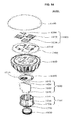
FIG. 14 is a view showing alighting apparatus 1000 including light emitting device packages according to an embodiment. - Referring to
FIG. 14 , thelighting apparatus 1000 may include acover 1100, alight source module 1200, aheat sink 1400, apower supply 1600, aninner case 1700, and asocket 1800. In addition, thelighting apparatus 1000 may further include at least one selected from between amember 1300 and aholder 1500. - The
light source module 1200 may include the light emitting device packages 100A to 100E shown inFIGs. 2 to 4 and8 to 11 or the light emittingdevice chips 130A to 130C shown inFIGs. 5A to 5C . - The
cover 1100 may be formed in the shape of a bulb or a hemisphere. Thecover 1100 may be hollow. A portion of thecover 1100 may be open. Thecover 1100 may be optically coupled to thelight source module 1200. For example, thecover 1100 may diffuse, scatter, or excite light emitted from thelight source module 1200. Thecover 1100 may be a kind of optical member. Thecover 1100 may be coupled to theheat sink 1400. Thecover 1100 may have a coupling part coupled to theheat sink 1400. - The inside of the
cover 1100 may be coated with a milky paint. The milky paint may include a diffusion material for diffusing light. The inside of thecover 110 may have surface roughness greater than that of the outside of thecover 1100 such that light emitted from thelight source module 1200 can be sufficiently scattered and diffused for exiting outward. - The
cover 1100 may be formed of glass, plastic, polypropylene (PP), polyethylene (PE), or polycarbonate (PC). PC exhibits high lightfastness, heat resistance, and strength. Thecover 1100 may be transparent such that thelight source module 1200 is visible from outside the cover. However, embodiments are not limited thereto. For example, thecover 1100 may be opaque. Thecover 1100 may be formed through blow molding. - The
light source module 1200 may be disposed at one surface of theheat sink 1400. Consequently, heat generated from thelight source module 1200 may be conducted to theheat sink 1400. Thelight source module 1200 may includelight source units 1210, aconnection plate 1230, and aconnector 1250. - The
member 1300 may be disposed on the top of theheat sink 1400. Themember 1300 hasguide grooves 1310, in which thelight source units 1210 and theconnector 1250 are inserted. Theguide grooves 1310 may correspond to or may be aligned with substrates of thelight source units 1210 and theconnector 1250. - A light reflective material may be applied to or coated on the surface of the
member 1300. - For example, a white paint may be applied to or coated on the surface of the
member 1300. Themember 1300 reflects light reflected by the inside of thecover 1100 and returning to thelight source module 1200 such that the light is directed to thecover 1100, thereby improving light efficiency of the lighting apparatus according to the embodiment. - The
member 1300 may be formed of an insulative material. Theconnection plate 1230 of thelight source module 1200 may include an electrically conductive material, by which electrical connection between theheat sink 1400 and theconnection plate 1230 may be achieved. Themember 1300 may be formed of an insulative material for preventing a short circuit between theconnection plate 1230 and theheat sink 1400. Theheat sink 1400 may dissipate heat generated from thelight source module 1200 and heat generated from thepower supply 1600. - The
holder 1500 blocks areception groove 1719 of aninsulative part 1710 of theinner case 1700. Consequently, thepower supply 1600 received in theinsulative part 1710 of theinner case 1700 may be hermetically sealed. Theholder 1500 may have aguide protrusion 1510. Theguide protrusion 1510 may have a hole through which aprotrusion 1610 of thepower supply 1600 passes. - The
power supply 1600 processes or converts an external electrical signal and supplies the processed or converted signal to thelight source module 1200. Thepower supply 1600 may be received in thereception groove 1719 of theinner case 1700 and may be hermetically sealed in theinner case 1700 by theholder 1500. Thepower supply 1600 may include aguide 1630, a base 1650, and anextension 1670 in addition to theprotrusion 1610. - The
guide 1630 may be formed in a shape protruding outward from one side of the base 1650. Theguide 1630 may be inserted into theholder 1500. A plurality of components may be disposed on one surface of the base 1650. The components may include a direct current converter for converting alternating current power supplied from an external power source into direct current power, a drive chip for controlling driving of thelight source module 1200, and an electrostatic discharge (ESD) protection device for protecting thelight source module 1200. However, embodiments are not limited thereto. - The
extension 1670 may be formed in a shape protruding outward from the other side of the base 1650. Theextension 1670 may be inserted into aconnection part 1750 of theinner case 1700 and receive an external electrical signal. For example, theextension 1670 may have a width equal to or less than that of theconnection part 1750 of theinner case 1700. One end of a positive cable and one end of a negative cable may be electrically connected to theextension 1670 and the other end of the positive cable and the other end of the negative cable may be electrically connected to thesocket 1800. - A molding part in addition to the
power supply 1600 may be disposed in theinner case 1700. The molding part, which is formed by solidified molding liquid, fixes thepower supply 1600 in theinner case 1700. - Although embodiments have been described with reference to a number of illustrative embodiments thereof, it should be understood that numerous other modifications and embodiments can be devised by those skilled in the art that will fall within the spirit and scope of the principles of this disclosure. More particularly, various variations and modifications are possible in the component parts and/or arrangements of the subject combination arrangement within the scope of the disclosure, the drawings and the appended claims. In addition to variations and modifications in the component parts and/or arrangements, alternative uses will also be apparent to those skilled in the art.
Claims (15)
- A light emitting device package, comprising:a package body;a light emitting device chip disposed on a chip mount area of the package body; anda molding member disposed on the package body,wherein the package body comprises:a central area having the chip mount area and a chip non-mount area adjacent to the chip mount area, the molding member being disposed on the central area; anda peripheral area around the central area, andwherein an upper surface of the light emitting device chip is higher than an upper surface of the package body in the chip non-mount area and than an upper surface of the package body in the peripheral area.
- The light emitting device package according to claim 1, wherein a lower surface of the light emitting device chip is higher than the upper surface of the package body in the chip non-mount area and than the upper surface of the package body in the peripheral area.
- The light emitting device package according to claim 1 or 2, wherein the central area comprises a first cavity in which the light emitting device chip is disposed.
- The light emitting device package according to any of claims 1 to 3, wherein the molding member is disposed to surround the light emitting device chip, and
wherein the package body comprises at least one molding groove defining a boundary of the molding member. - The light emitting device package according to claim 4, wherein the at least one molding groove is disposed in the peripheral area on the package body at an interface between the peripheral area and the central area.
- The light emitting device package according to claim 4 or 5, wherein the molding member is disposed to extend up to an inside edge of the at least one molding groove.
- The light emitting device package according to claim 4 or 5, wherein the molding member is disposed to extend up to an outer edge of the at least one molding groove.
- The light emitting device package according to any of claims 1 to 3, further comprising a dam disposed on the peripheral area on the package body at an interface between the peripheral area and the central area, the dam defining a second cavity.
- The light emitting device package according to claim 8, wherein a top surface of the dam is higher than the upper surface of the light emitting device chip.
- The light emitting device package according to claim 9, wherein the dam comprises a transparent material.
- The light emitting device package according to claim 8, wherein a top surface of the dam is lower than the upper surface of the light emitting device chip.
- The light emitting device package according to claim 11, wherein the top surface of the dam is lower than a lower surface of the light emitting device chip.
- The light emitting device package according to any of claims 8, 11, and 12, wherein the molding member is disposed to extend up to an inner wall of the dam while filling the second cavity.
- The light emitting device package according to claim 9 or 10, wherein the molding member is put on the dam for covering the second cavity.
- The light emitting device package according to claim 14, wherein the second cavity is under vacuum.
Applications Claiming Priority (1)
| Application Number | Priority Date | Filing Date | Title |
|---|---|---|---|
| KR1020130108963A KR102080778B1 (en) | 2013-09-11 | 2013-09-11 | Light emitting device package |
Publications (3)
| Publication Number | Publication Date |
|---|---|
| EP2858131A2 true EP2858131A2 (en) | 2015-04-08 |
| EP2858131A3 EP2858131A3 (en) | 2016-02-17 |
| EP2858131B1 EP2858131B1 (en) | 2022-12-21 |
Family
ID=51265614
Family Applications (1)
| Application Number | Title | Priority Date | Filing Date |
|---|---|---|---|
| EP14179994.0A Active EP2858131B1 (en) | 2013-09-11 | 2014-08-06 | Light emitting device package |
Country Status (4)
| Country | Link |
|---|---|
| US (1) | US9472728B2 (en) |
| EP (1) | EP2858131B1 (en) |
| KR (1) | KR102080778B1 (en) |
| CN (1) | CN104425685B (en) |
Cited By (2)
| Publication number | Priority date | Publication date | Assignee | Title |
|---|---|---|---|---|
| EP3091822A1 (en) * | 2015-05-08 | 2016-11-09 | AT & S Austria Technologie & Systemtechnik Aktiengesellschaft | Method for the production of an electronic module as well as corresponding electronic module |
| WO2025168383A1 (en) * | 2024-02-08 | 2025-08-14 | Ams-Osram International Gmbh | Optoelectronic component |
Families Citing this family (12)
| Publication number | Priority date | Publication date | Assignee | Title |
|---|---|---|---|---|
| US20170104135A1 (en) * | 2015-10-13 | 2017-04-13 | Sensor Electronic Technology, Inc. | Light Emitting Diode Mounting Structure |
| KR101781748B1 (en) * | 2016-09-01 | 2017-09-25 | 주식회사 루멘스 | Uv led package |
| US20200098957A1 (en) * | 2017-01-18 | 2020-03-26 | Cree Huizhou Solid State Lighting Company Ltd. | Multiple led light source lens design in an integrated package |
| DE102017128717B4 (en) * | 2017-12-04 | 2023-03-09 | OSRAM Opto Semiconductors Gesellschaft mit beschränkter Haftung | Process for producing an optoelectronic component |
| JP7037053B2 (en) * | 2018-04-25 | 2022-03-16 | 日亜化学工業株式会社 | Manufacturing method of light emitting device and light emitting device |
| CN108954201A (en) * | 2018-09-12 | 2018-12-07 | Tcl华瑞照明科技(惠州)有限公司 | LED lamp bead and LED illumination lamp |
| CN112820810A (en) * | 2019-11-18 | 2021-05-18 | 佛山市国星光电股份有限公司 | A LED device, LED device array and plastic packaging mold |
| US11769862B2 (en) * | 2020-03-26 | 2023-09-26 | Nichia Corporation | Light emitting device |
| JP7121312B2 (en) * | 2020-03-26 | 2022-08-18 | 日亜化学工業株式会社 | light emitting device |
| DE102021128151A1 (en) | 2021-10-28 | 2023-05-04 | OSRAM Opto Semiconductors Gesellschaft mit beschränkter Haftung | METHOD FOR MANUFACTURING OPTOELECTRONIC DEVICE AND OPTOELECTRONIC DEVICE |
| KR20230068198A (en) * | 2021-11-10 | 2023-05-17 | 삼성전자주식회사 | Uv light source and method of manufacturing the same |
| CN116995170B (en) * | 2023-05-24 | 2024-11-15 | 佛山大学 | Electrode packaging structure and light-emitting module |
Family Cites Families (16)
| Publication number | Priority date | Publication date | Assignee | Title |
|---|---|---|---|---|
| DE29724847U1 (en) * | 1996-06-26 | 2004-09-30 | Osram Opto Semiconductors Gmbh | Light-emitting semiconductor component with luminescence conversion element |
| JP4961799B2 (en) * | 2005-04-08 | 2012-06-27 | 日亜化学工業株式会社 | Light emitting device having a silicone resin layer formed by screen printing |
| JP3992059B2 (en) * | 2005-11-21 | 2007-10-17 | 松下電工株式会社 | Method for manufacturing light emitting device |
| US7473940B2 (en) * | 2006-11-27 | 2009-01-06 | Avago Technologies Ecbu Ip (Singapore) Pte. Ltd. | Compact LED with a self-formed encapsulating dome |
| JP4888280B2 (en) * | 2007-08-28 | 2012-02-29 | パナソニック電工株式会社 | Light emitting device |
| US7800125B2 (en) * | 2008-07-09 | 2010-09-21 | Himax Display, Inc. | Light-emitting diode package |
| WO2011007874A1 (en) * | 2009-07-17 | 2011-01-20 | 電気化学工業株式会社 | Led chip assembly, led package, and manufacturing method of led package |
| KR101114794B1 (en) * | 2009-10-26 | 2012-03-09 | 엘지이노텍 주식회사 | Light emitting device package and method for fabricating the same |
| KR101154656B1 (en) * | 2010-08-09 | 2012-06-08 | 엘지이노텍 주식회사 | Light emitting device and lighing system |
| TWI533483B (en) * | 2010-08-09 | 2016-05-11 | Lg伊諾特股份有限公司 | Illuminating device |
| KR101303168B1 (en) * | 2011-07-26 | 2013-09-09 | 안상정 | Conneted body with semiconductor light emitting regions |
| KR101846356B1 (en) * | 2011-07-29 | 2018-04-09 | 엘지이노텍 주식회사 | Optical component package and manufacturing method thereof |
| JP5545279B2 (en) * | 2011-09-20 | 2014-07-09 | 豊田合成株式会社 | Surface light source device |
| DE102011115150A1 (en) * | 2011-09-27 | 2013-03-28 | Osram Opto Semiconductors Gmbh | Method for producing at least one radiation-emitting and / or receiving semiconductor component and semiconductor component |
| JP2014044970A (en) * | 2011-12-14 | 2014-03-13 | Mitsubishi Electric Corp | Light emitting device and manufacturing method of the same |
| JP6147977B2 (en) * | 2012-09-26 | 2017-06-14 | ローム株式会社 | LED lighting apparatus and LED unit |
-
2013
- 2013-09-11 KR KR1020130108963A patent/KR102080778B1/en not_active Expired - Fee Related
-
2014
- 2014-08-06 EP EP14179994.0A patent/EP2858131B1/en active Active
- 2014-08-25 CN CN201410423052.XA patent/CN104425685B/en active Active
- 2014-09-10 US US14/482,466 patent/US9472728B2/en active Active
Non-Patent Citations (1)
| Title |
|---|
| None |
Cited By (3)
| Publication number | Priority date | Publication date | Assignee | Title |
|---|---|---|---|---|
| EP3091822A1 (en) * | 2015-05-08 | 2016-11-09 | AT & S Austria Technologie & Systemtechnik Aktiengesellschaft | Method for the production of an electronic module as well as corresponding electronic module |
| US10283680B2 (en) | 2015-05-08 | 2019-05-07 | At&S Austria Technologie & Systemtechnik Aktiengesellschaft | Method for the production of an electronic module having an electronic component embedded therein |
| WO2025168383A1 (en) * | 2024-02-08 | 2025-08-14 | Ams-Osram International Gmbh | Optoelectronic component |
Also Published As
| Publication number | Publication date |
|---|---|
| EP2858131A3 (en) | 2016-02-17 |
| CN104425685B (en) | 2018-11-23 |
| US20150070909A1 (en) | 2015-03-12 |
| EP2858131B1 (en) | 2022-12-21 |
| US9472728B2 (en) | 2016-10-18 |
| CN104425685A (en) | 2015-03-18 |
| KR102080778B1 (en) | 2020-04-14 |
| KR20150029919A (en) | 2015-03-19 |
Similar Documents
| Publication | Publication Date | Title |
|---|---|---|
| EP2858131B1 (en) | Light emitting device package | |
| EP2587555B1 (en) | Light emitting device | |
| EP2587541B1 (en) | Light emitting device | |
| EP2728632A2 (en) | Light emitting device and light emitting device array | |
| US9252340B2 (en) | Phosphor and light emitting device package including the same | |
| CN104103719A (en) | Light emitting device and package of light emitting device | |
| EP2849237A1 (en) | Light emitting device package | |
| JP6510763B2 (en) | Light emitting device package | |
| EP2565921A1 (en) | Light emitting device | |
| JP6878406B2 (en) | Light emitting element and light emitting element package containing it | |
| KR102127445B1 (en) | Light Emitting Device Package | |
| KR20160086559A (en) | Light emitting device, light emitting device package having the same, and light system having the same | |
| CN104241481A (en) | Light emitting device and lighting system | |
| KR102170216B1 (en) | Light emitting device and light emitting device package | |
| EP3029746A1 (en) | Light emitting device | |
| EP3048650B1 (en) | Light emitting device | |
| KR102309671B1 (en) | Light emitting device package and lighiting device | |
| KR102114932B1 (en) | Light emitting device and package including the device | |
| KR20150029920A (en) | Light Emitting Device and Light Emitting Device Package | |
| KR102050057B1 (en) | Light Emitting Device Package | |
| KR102153125B1 (en) | Light emitting device and lighting system | |
| KR102080777B1 (en) | Light emitting device and light emitting module including the device | |
| KR20160007195A (en) | Light emitting device package | |
| KR20150025600A (en) | Light Emitting Device | |
| KR20160089142A (en) | Light source module and lighting device |
Legal Events
| Date | Code | Title | Description |
|---|---|---|---|
| PUAI | Public reference made under article 153(3) epc to a published international application that has entered the european phase |
Free format text: ORIGINAL CODE: 0009012 |
|
| 17P | Request for examination filed |
Effective date: 20140806 |
|
| AK | Designated contracting states |
Kind code of ref document: A2 Designated state(s): AL AT BE BG CH CY CZ DE DK EE ES FI FR GB GR HR HU IE IS IT LI LT LU LV MC MK MT NL NO PL PT RO RS SE SI SK SM TR |
|
| AX | Request for extension of the european patent |
Extension state: BA ME |
|
| PUAL | Search report despatched |
Free format text: ORIGINAL CODE: 0009013 |
|
| AK | Designated contracting states |
Kind code of ref document: A3 Designated state(s): AL AT BE BG CH CY CZ DE DK EE ES FI FR GB GR HR HU IE IS IT LI LT LU LV MC MK MT NL NO PL PT RO RS SE SI SK SM TR |
|
| AX | Request for extension of the european patent |
Extension state: BA ME |
|
| RIC1 | Information provided on ipc code assigned before grant |
Ipc: H01L 33/54 20100101ALI20160113BHEP Ipc: H01L 33/62 20100101ALN20160113BHEP Ipc: H01L 33/48 20100101AFI20160113BHEP |
|
| R17P | Request for examination filed (corrected) |
Effective date: 20160708 |
|
| RBV | Designated contracting states (corrected) |
Designated state(s): AL AT BE BG CH CY CZ DE DK EE ES FI FR GB GR HR HU IE IS IT LI LT LU LV MC MK MT NL NO PL PT RO RS SE SI SK SM TR |
|
| RAP1 | Party data changed (applicant data changed or rights of an application transferred) |
Owner name: LG INNOTEK CO., LTD. |
|
| STAA | Information on the status of an ep patent application or granted ep patent |
Free format text: STATUS: EXAMINATION IS IN PROGRESS |
|
| 17Q | First examination report despatched |
Effective date: 20200212 |
|
| RAP1 | Party data changed (applicant data changed or rights of an application transferred) |
Owner name: SUZHOU LEKIN SEMICONDUCTOR CO., LTD. |
|
| RIC1 | Information provided on ipc code assigned before grant |
Ipc: F21Y 115/10 20160101ALN20220615BHEP Ipc: H01L 33/62 20100101ALN20220615BHEP Ipc: F21V 3/10 20180101ALI20220615BHEP Ipc: H01L 33/54 20100101ALI20220615BHEP Ipc: H01L 33/48 20100101AFI20220615BHEP |
|
| GRAP | Despatch of communication of intention to grant a patent |
Free format text: ORIGINAL CODE: EPIDOSNIGR1 |
|
| STAA | Information on the status of an ep patent application or granted ep patent |
Free format text: STATUS: GRANT OF PATENT IS INTENDED |
|
| RIC1 | Information provided on ipc code assigned before grant |
Ipc: F21Y 115/10 20160101ALN20220711BHEP Ipc: H01L 33/62 20100101ALN20220711BHEP Ipc: F21V 3/10 20180101ALI20220711BHEP Ipc: H01L 33/54 20100101ALI20220711BHEP Ipc: H01L 33/48 20100101AFI20220711BHEP |
|
| INTG | Intention to grant announced |
Effective date: 20220803 |
|
| RIN1 | Information on inventor provided before grant (corrected) |
Inventor name: OH, JUNG HUN Inventor name: JUNG, KYEOUNG AN |
|
| GRAS | Grant fee paid |
Free format text: ORIGINAL CODE: EPIDOSNIGR3 |
|
| GRAA | (expected) grant |
Free format text: ORIGINAL CODE: 0009210 |
|
| STAA | Information on the status of an ep patent application or granted ep patent |
Free format text: STATUS: THE PATENT HAS BEEN GRANTED |
|
| AK | Designated contracting states |
Kind code of ref document: B1 Designated state(s): AL AT BE BG CH CY CZ DE DK EE ES FI FR GB GR HR HU IE IS IT LI LT LU LV MC MK MT NL NO PL PT RO RS SE SI SK SM TR |
|
| REG | Reference to a national code |
Ref country code: GB Ref legal event code: FG4D |
|
| REG | Reference to a national code |
Ref country code: CH Ref legal event code: EP |
|
| REG | Reference to a national code |
Ref country code: DE Ref legal event code: R096 Ref document number: 602014085846 Country of ref document: DE |
|
| REG | Reference to a national code |
Ref country code: AT Ref legal event code: REF Ref document number: 1539583 Country of ref document: AT Kind code of ref document: T Effective date: 20230115 |
|
| REG | Reference to a national code |
Ref country code: IE Ref legal event code: FG4D |
|
| REG | Reference to a national code |
Ref country code: LT Ref legal event code: MG9D |
|
| REG | Reference to a national code |
Ref country code: NL Ref legal event code: MP Effective date: 20221221 |
|
| PG25 | Lapsed in a contracting state [announced via postgrant information from national office to epo] |
Ref country code: SE Free format text: LAPSE BECAUSE OF FAILURE TO SUBMIT A TRANSLATION OF THE DESCRIPTION OR TO PAY THE FEE WITHIN THE PRESCRIBED TIME-LIMIT Effective date: 20221221 Ref country code: NO Free format text: LAPSE BECAUSE OF FAILURE TO SUBMIT A TRANSLATION OF THE DESCRIPTION OR TO PAY THE FEE WITHIN THE PRESCRIBED TIME-LIMIT Effective date: 20230321 Ref country code: LT Free format text: LAPSE BECAUSE OF FAILURE TO SUBMIT A TRANSLATION OF THE DESCRIPTION OR TO PAY THE FEE WITHIN THE PRESCRIBED TIME-LIMIT Effective date: 20221221 Ref country code: FI Free format text: LAPSE BECAUSE OF FAILURE TO SUBMIT A TRANSLATION OF THE DESCRIPTION OR TO PAY THE FEE WITHIN THE PRESCRIBED TIME-LIMIT Effective date: 20221221 |
|
| REG | Reference to a national code |
Ref country code: AT Ref legal event code: MK05 Ref document number: 1539583 Country of ref document: AT Kind code of ref document: T Effective date: 20221221 |
|
| PG25 | Lapsed in a contracting state [announced via postgrant information from national office to epo] |
Ref country code: RS Free format text: LAPSE BECAUSE OF FAILURE TO SUBMIT A TRANSLATION OF THE DESCRIPTION OR TO PAY THE FEE WITHIN THE PRESCRIBED TIME-LIMIT Effective date: 20221221 Ref country code: LV Free format text: LAPSE BECAUSE OF FAILURE TO SUBMIT A TRANSLATION OF THE DESCRIPTION OR TO PAY THE FEE WITHIN THE PRESCRIBED TIME-LIMIT Effective date: 20221221 Ref country code: HR Free format text: LAPSE BECAUSE OF FAILURE TO SUBMIT A TRANSLATION OF THE DESCRIPTION OR TO PAY THE FEE WITHIN THE PRESCRIBED TIME-LIMIT Effective date: 20221221 Ref country code: GR Free format text: LAPSE BECAUSE OF FAILURE TO SUBMIT A TRANSLATION OF THE DESCRIPTION OR TO PAY THE FEE WITHIN THE PRESCRIBED TIME-LIMIT Effective date: 20230322 |
|
| PG25 | Lapsed in a contracting state [announced via postgrant information from national office to epo] |
Ref country code: NL Free format text: LAPSE BECAUSE OF FAILURE TO SUBMIT A TRANSLATION OF THE DESCRIPTION OR TO PAY THE FEE WITHIN THE PRESCRIBED TIME-LIMIT Effective date: 20221221 |
|
| PG25 | Lapsed in a contracting state [announced via postgrant information from national office to epo] |
Ref country code: SM Free format text: LAPSE BECAUSE OF FAILURE TO SUBMIT A TRANSLATION OF THE DESCRIPTION OR TO PAY THE FEE WITHIN THE PRESCRIBED TIME-LIMIT Effective date: 20221221 Ref country code: RO Free format text: LAPSE BECAUSE OF FAILURE TO SUBMIT A TRANSLATION OF THE DESCRIPTION OR TO PAY THE FEE WITHIN THE PRESCRIBED TIME-LIMIT Effective date: 20221221 Ref country code: PT Free format text: LAPSE BECAUSE OF FAILURE TO SUBMIT A TRANSLATION OF THE DESCRIPTION OR TO PAY THE FEE WITHIN THE PRESCRIBED TIME-LIMIT Effective date: 20230421 Ref country code: ES Free format text: LAPSE BECAUSE OF FAILURE TO SUBMIT A TRANSLATION OF THE DESCRIPTION OR TO PAY THE FEE WITHIN THE PRESCRIBED TIME-LIMIT Effective date: 20221221 Ref country code: EE Free format text: LAPSE BECAUSE OF FAILURE TO SUBMIT A TRANSLATION OF THE DESCRIPTION OR TO PAY THE FEE WITHIN THE PRESCRIBED TIME-LIMIT Effective date: 20221221 Ref country code: CZ Free format text: LAPSE BECAUSE OF FAILURE TO SUBMIT A TRANSLATION OF THE DESCRIPTION OR TO PAY THE FEE WITHIN THE PRESCRIBED TIME-LIMIT Effective date: 20221221 Ref country code: AT Free format text: LAPSE BECAUSE OF FAILURE TO SUBMIT A TRANSLATION OF THE DESCRIPTION OR TO PAY THE FEE WITHIN THE PRESCRIBED TIME-LIMIT Effective date: 20221221 |
|
| PG25 | Lapsed in a contracting state [announced via postgrant information from national office to epo] |
Ref country code: SK Free format text: LAPSE BECAUSE OF FAILURE TO SUBMIT A TRANSLATION OF THE DESCRIPTION OR TO PAY THE FEE WITHIN THE PRESCRIBED TIME-LIMIT Effective date: 20221221 Ref country code: PL Free format text: LAPSE BECAUSE OF FAILURE TO SUBMIT A TRANSLATION OF THE DESCRIPTION OR TO PAY THE FEE WITHIN THE PRESCRIBED TIME-LIMIT Effective date: 20221221 Ref country code: IS Free format text: LAPSE BECAUSE OF FAILURE TO SUBMIT A TRANSLATION OF THE DESCRIPTION OR TO PAY THE FEE WITHIN THE PRESCRIBED TIME-LIMIT Effective date: 20230421 Ref country code: AL Free format text: LAPSE BECAUSE OF FAILURE TO SUBMIT A TRANSLATION OF THE DESCRIPTION OR TO PAY THE FEE WITHIN THE PRESCRIBED TIME-LIMIT Effective date: 20221221 |
|
| REG | Reference to a national code |
Ref country code: DE Ref legal event code: R097 Ref document number: 602014085846 Country of ref document: DE |
|
| PLBE | No opposition filed within time limit |
Free format text: ORIGINAL CODE: 0009261 |
|
| STAA | Information on the status of an ep patent application or granted ep patent |
Free format text: STATUS: NO OPPOSITION FILED WITHIN TIME LIMIT |
|
| PG25 | Lapsed in a contracting state [announced via postgrant information from national office to epo] |
Ref country code: DK Free format text: LAPSE BECAUSE OF FAILURE TO SUBMIT A TRANSLATION OF THE DESCRIPTION OR TO PAY THE FEE WITHIN THE PRESCRIBED TIME-LIMIT Effective date: 20221221 |
|
| 26N | No opposition filed |
Effective date: 20230922 |
|
| PG25 | Lapsed in a contracting state [announced via postgrant information from national office to epo] |
Ref country code: SI Free format text: LAPSE BECAUSE OF FAILURE TO SUBMIT A TRANSLATION OF THE DESCRIPTION OR TO PAY THE FEE WITHIN THE PRESCRIBED TIME-LIMIT Effective date: 20221221 |
|
| PG25 | Lapsed in a contracting state [announced via postgrant information from national office to epo] |
Ref country code: MC Free format text: LAPSE BECAUSE OF FAILURE TO SUBMIT A TRANSLATION OF THE DESCRIPTION OR TO PAY THE FEE WITHIN THE PRESCRIBED TIME-LIMIT Effective date: 20221221 |
|
| REG | Reference to a national code |
Ref country code: CH Ref legal event code: PL |
|
| PG25 | Lapsed in a contracting state [announced via postgrant information from national office to epo] |
Ref country code: MC Free format text: LAPSE BECAUSE OF FAILURE TO SUBMIT A TRANSLATION OF THE DESCRIPTION OR TO PAY THE FEE WITHIN THE PRESCRIBED TIME-LIMIT Effective date: 20221221 |
|
| PG25 | Lapsed in a contracting state [announced via postgrant information from national office to epo] |
Ref country code: LU Free format text: LAPSE BECAUSE OF NON-PAYMENT OF DUE FEES Effective date: 20230806 |
|
| GBPC | Gb: european patent ceased through non-payment of renewal fee |
Effective date: 20230806 |
|
| PG25 | Lapsed in a contracting state [announced via postgrant information from national office to epo] |
Ref country code: LU Free format text: LAPSE BECAUSE OF NON-PAYMENT OF DUE FEES Effective date: 20230806 Ref country code: CH Free format text: LAPSE BECAUSE OF NON-PAYMENT OF DUE FEES Effective date: 20230831 |
|
| REG | Reference to a national code |
Ref country code: BE Ref legal event code: MM Effective date: 20230831 |
|
| REG | Reference to a national code |
Ref country code: IE Ref legal event code: MM4A |
|
| PG25 | Lapsed in a contracting state [announced via postgrant information from national office to epo] |
Ref country code: IT Free format text: LAPSE BECAUSE OF FAILURE TO SUBMIT A TRANSLATION OF THE DESCRIPTION OR TO PAY THE FEE WITHIN THE PRESCRIBED TIME-LIMIT Effective date: 20221221 |
|
| PG25 | Lapsed in a contracting state [announced via postgrant information from national office to epo] |
Ref country code: IE Free format text: LAPSE BECAUSE OF NON-PAYMENT OF DUE FEES Effective date: 20230806 |
|
| PG25 | Lapsed in a contracting state [announced via postgrant information from national office to epo] |
Ref country code: GB Free format text: LAPSE BECAUSE OF NON-PAYMENT OF DUE FEES Effective date: 20230806 |
|
| PG25 | Lapsed in a contracting state [announced via postgrant information from national office to epo] |
Ref country code: IE Free format text: LAPSE BECAUSE OF NON-PAYMENT OF DUE FEES Effective date: 20230806 Ref country code: GB Free format text: LAPSE BECAUSE OF NON-PAYMENT OF DUE FEES Effective date: 20230806 Ref country code: FR Free format text: LAPSE BECAUSE OF NON-PAYMENT OF DUE FEES Effective date: 20230831 |
|
| PG25 | Lapsed in a contracting state [announced via postgrant information from national office to epo] |
Ref country code: BE Free format text: LAPSE BECAUSE OF NON-PAYMENT OF DUE FEES Effective date: 20230831 |
|
| PGFP | Annual fee paid to national office [announced via postgrant information from national office to epo] |
Ref country code: DE Payment date: 20240709 Year of fee payment: 11 |
|
| PG25 | Lapsed in a contracting state [announced via postgrant information from national office to epo] |
Ref country code: BG Free format text: LAPSE BECAUSE OF FAILURE TO SUBMIT A TRANSLATION OF THE DESCRIPTION OR TO PAY THE FEE WITHIN THE PRESCRIBED TIME-LIMIT Effective date: 20221221 |
|
| REG | Reference to a national code |
Ref country code: DE Ref legal event code: R079 Ref document number: 602014085846 Country of ref document: DE Free format text: PREVIOUS MAIN CLASS: H01L0033480000 Ipc: H10H0020850000 |
|
| PG25 | Lapsed in a contracting state [announced via postgrant information from national office to epo] |
Ref country code: BG Free format text: LAPSE BECAUSE OF FAILURE TO SUBMIT A TRANSLATION OF THE DESCRIPTION OR TO PAY THE FEE WITHIN THE PRESCRIBED TIME-LIMIT Effective date: 20221221 |
|
| PG25 | Lapsed in a contracting state [announced via postgrant information from national office to epo] |
Ref country code: CY Free format text: LAPSE BECAUSE OF FAILURE TO SUBMIT A TRANSLATION OF THE DESCRIPTION OR TO PAY THE FEE WITHIN THE PRESCRIBED TIME-LIMIT; INVALID AB INITIO Effective date: 20140806 |
|
| PG25 | Lapsed in a contracting state [announced via postgrant information from national office to epo] |
Ref country code: HU Free format text: LAPSE BECAUSE OF FAILURE TO SUBMIT A TRANSLATION OF THE DESCRIPTION OR TO PAY THE FEE WITHIN THE PRESCRIBED TIME-LIMIT; INVALID AB INITIO Effective date: 20140806 |
|
| PG25 | Lapsed in a contracting state [announced via postgrant information from national office to epo] |
Ref country code: TR Free format text: LAPSE BECAUSE OF FAILURE TO SUBMIT A TRANSLATION OF THE DESCRIPTION OR TO PAY THE FEE WITHIN THE PRESCRIBED TIME-LIMIT Effective date: 20221221 |
|
| REG | Reference to a national code |
Ref country code: DE Ref legal event code: R119 Ref document number: 602014085846 Country of ref document: DE |