EP2856563B1 - Circuit électrique pour l'interconnexion d'un composant électrique, tel qu'un composant de puissance - Google Patents
Circuit électrique pour l'interconnexion d'un composant électrique, tel qu'un composant de puissance Download PDFInfo
- Publication number
- EP2856563B1 EP2856563B1 EP13731378.9A EP13731378A EP2856563B1 EP 2856563 B1 EP2856563 B1 EP 2856563B1 EP 13731378 A EP13731378 A EP 13731378A EP 2856563 B1 EP2856563 B1 EP 2856563B1
- Authority
- EP
- European Patent Office
- Prior art keywords
- contact
- electrical
- component
- flex circuit
- circuit according
- Prior art date
- Legal status (The legal status is an assumption and is not a legal conclusion. Google has not performed a legal analysis and makes no representation as to the accuracy of the status listed.)
- Active
Links
Images
Classifications
-
- H—ELECTRICITY
- H01—ELECTRIC ELEMENTS
- H01R—ELECTRICALLY-CONDUCTIVE CONNECTIONS; STRUCTURAL ASSOCIATIONS OF A PLURALITY OF MUTUALLY-INSULATED ELECTRICAL CONNECTING ELEMENTS; COUPLING DEVICES; CURRENT COLLECTORS
- H01R12/00—Structural associations of a plurality of mutually-insulated electrical connecting elements, specially adapted for printed circuits, e.g. printed circuit boards [PCB], flat or ribbon cables, or like generally planar structures, e.g. terminal strips, terminal blocks; Coupling devices specially adapted for printed circuits, flat or ribbon cables, or like generally planar structures; Terminals specially adapted for contact with, or insertion into, printed circuits, flat or ribbon cables, or like generally planar structures
- H01R12/50—Fixed connections
- H01R12/51—Fixed connections for rigid printed circuits or like structures
- H01R12/55—Fixed connections for rigid printed circuits or like structures characterised by the terminals
- H01R12/57—Fixed connections for rigid printed circuits or like structures characterised by the terminals surface mounting terminals
-
- H—ELECTRICITY
- H01—ELECTRIC ELEMENTS
- H01R—ELECTRICALLY-CONDUCTIVE CONNECTIONS; STRUCTURAL ASSOCIATIONS OF A PLURALITY OF MUTUALLY-INSULATED ELECTRICAL CONNECTING ELEMENTS; COUPLING DEVICES; CURRENT COLLECTORS
- H01R12/00—Structural associations of a plurality of mutually-insulated electrical connecting elements, specially adapted for printed circuits, e.g. printed circuit boards [PCB], flat or ribbon cables, or like generally planar structures, e.g. terminal strips, terminal blocks; Coupling devices specially adapted for printed circuits, flat or ribbon cables, or like generally planar structures; Terminals specially adapted for contact with, or insertion into, printed circuits, flat or ribbon cables, or like generally planar structures
- H01R12/50—Fixed connections
- H01R12/59—Fixed connections for flexible printed circuits, flat or ribbon cables or like structures
- H01R12/592—Fixed connections for flexible printed circuits, flat or ribbon cables or like structures connections to contact elements
-
- H—ELECTRICITY
- H01—ELECTRIC ELEMENTS
- H01R—ELECTRICALLY-CONDUCTIVE CONNECTIONS; STRUCTURAL ASSOCIATIONS OF A PLURALITY OF MUTUALLY-INSULATED ELECTRICAL CONNECTING ELEMENTS; COUPLING DEVICES; CURRENT COLLECTORS
- H01R12/00—Structural associations of a plurality of mutually-insulated electrical connecting elements, specially adapted for printed circuits, e.g. printed circuit boards [PCB], flat or ribbon cables, or like generally planar structures, e.g. terminal strips, terminal blocks; Coupling devices specially adapted for printed circuits, flat or ribbon cables, or like generally planar structures; Terminals specially adapted for contact with, or insertion into, printed circuits, flat or ribbon cables, or like generally planar structures
- H01R12/50—Fixed connections
- H01R12/59—Fixed connections for flexible printed circuits, flat or ribbon cables or like structures
- H01R12/61—Fixed connections for flexible printed circuits, flat or ribbon cables or like structures connecting to flexible printed circuits, flat or ribbon cables or like structures
- H01R12/613—Fixed connections for flexible printed circuits, flat or ribbon cables or like structures connecting to flexible printed circuits, flat or ribbon cables or like structures by means of interconnecting elements
- H01R12/616—Fixed connections for flexible printed circuits, flat or ribbon cables or like structures connecting to flexible printed circuits, flat or ribbon cables or like structures by means of interconnecting elements having contacts penetrating insulation for making contact with conductors, e.g. needle points
Definitions
- the invention relates to an electrical circuit comprising flexible electrical circuits called flex circuits, and the application of this circuit to the interconnection of power converters intended in particular to be embedded, in particular integrated in harsh environments and in the management of currents. between 1A and 200A.
- the invention applies in particular to the control electronics of aircraft actuators, such as braking actuators, flight control actuators, etc.
- low-power converters are generally composed of power switches that provide modulation of energy transfer from one electrical network to another, decoupling capacitors that absorb the energy transfer modulation and a power supply. electronics that controls these switches according to a logic defined by the user.
- the transfer of energy is controlled by a transfer modulation, called switching, which consists of alternating coupling and decoupling of the two networks, one network is treated by the switches as a voltage source and the other network as a Power source.
- the integration of the power switches with the decoupling capacitors is a key point of the operation of the system because the dynamics of the switching currents of the power source by the power switches is important.
- the solutions currently used to limit overvoltage problems is to position the metallic conductive elements of the voltage source so as to minimize the parasitic interconnection inductance between the voltage switches. power and decoupling capability, in particular by superimposing these conductive elements.
- the low-power converters are made from so-called discrete power components and passive components such as capacitors and inductors, and are integrated on rigid multilayer printed circuit boards, called PCB ("printed circuit board" in English). ), or from power modules and passive components interconnected via a rigid busbar electric circuit, called rigid busbar, composed of layers of conductors separated from each other by layers of electrical insulation.
- PCB printed circuit board
- thermomechanical constraints related to the integration of the multiple materials involved metallic polymers, etc.
- thermomechanical constraints related to the integration of the multiple materials involved (metallic polymers, etc.), which have different own thermal expansion constants, and therefore is likely to generate significant thermomechanical stresses on the contact parts, including contact solder joints of the assembly, which limits the life and reliability of the latter.
- the so-called discrete power components for example pinned electrical modules, are mounted on a rigid card carrier (PCB) consisting of a succession of layers of insulators and conductors.
- PCB rigid card carrier
- the control of the power components is usually embedded on this map.
- This assembly solution practical and of a relevant cost, is generally used for the realization of converters of low or medium power. In addition, it integrates the interconnection of power components and control components.
- this component assembly solution does not offer an ease of physical integration of these components in the three axes of space or in 3D and its lifetime as well as the reliability of operation remain limited, in particular in the case of high thermal cycles and / or frequent operation.
- the power components are generally carried on a rigid support that can be shaped by folding, generally composed of layers of conductors separated layers of electrical insulation.
- the connection with the control of the components is done via connections on power modules.
- These assemblies are of high cost, being generally used for the realization of medium and high power converters. They offer integration facilities 3 D components that remain limited, however.
- the removable screw-nut interconnection means that can be used limit the mechanical integration of the components and increase the assembly costs.
- US5277595 describes a connection for computer cards
- WO 2007087982 discloses an electric circuit according to the preamble of claim 1.
- the invention aims to provide an interconnection of power components on embedded electrical circuit assemblies, in particular integrated in harsh environments and ensuring the management of currents greater than 1A and less than 200A.
- An electric circuit according to claim 1 is provided.
- homogeneous current density is meant a substantially constant current density at any point on the contact surface.
- Said current density is advantageously between 4.5 and 5.5 A / mm 2 , preferably between 4.8 and 5.2 A / mm 2 and in particular is equal to 5 A / mm 2 .
- Such an electrical circuit thus makes it possible to connect an electrical power component to an electric flex circuit, a relatively flexible circuit and therefore adaptable to 3 D in an available space, by limiting the current density on the contacts, which has the effect of reducing on the one hand, the current transmission heating on the contact parts and on the other hand, the mechanical stresses on the contact parts.
- This control of the current flow density on the contact parts of the component to the flex circuit then allows the latter to withstand a greater electric current than that of a conventional assembly and therefore allows a connection of a power component to the flex circuit thus equipped in currents between 1 and 200 A, in particular currents from 30 to 80 A.
- Said electrically conductive part is advantageously a metal part, preferably made of copper, brass or aluminum, having relatively large and massive contact parts, which makes it possible to control the density of flow of the current in the contact zone and to absorb the local concentrations of mechanical stress in this contact zone.
- the electrical conductive part may be in the form of a cylindrical sleeve or a cylindrical sleeve portion provided with a flat ring, the first contact portion being formed by the cylindrical inner face of the sleeve or the sleeve portion and the second contact portion is constituted by a face of the crown.
- the width range of said second contact portion may in particular correspond to the width of the flex circuit.
- the lengthwise extent (transverse to the width) of the second contact portion is then adjusted to provide a clean contact surface for transmitting said electrical current density below 20 A / mm 2 .
- said electrical conductive part is advantageously shaped to allow a junction of the contact parts with the flex circuit and the component that can be performed in a given joining method, for example soft or hard soldering, electrical or laser welding, sintering etc.
- the first contact portion may have a complementary surface of the contact element of the component, for example the pin or contact tab of the component, being shaped to come into contact with the contact element of the component, in particular the said pin of contact or said contact tab of the component.
- the second contact portion may have a flat surface shaped to come into plane contact with said conductive layer of the flex circuit.
- the electrical conductive part or current diffuser advantageously has the shape of a cylindrical sleeve provided with a flat ring at one of its ends or on its periphery, being shaped to come into contact with a pin pin of component by the cylindrical inner face of the sleeve and come into contact with a conductive layer of the flex circuit by an outer face of the ring.
- the first contact portion is thus constituted by at least a portion of the cylindrical inner face of the sleeve.
- the second contact portion is then constituted by said outer face of the ring.
- the first contact portion may further be cylinder portion-shaped, contacting an end portion of a contact pin of the electrical component and a portion of the contact pin section, and the second portion contact is a flat ring applied by its outer surface to the surface of the lower conductive layer of the flex circuit.
- the contact pin or pin pin can be further mounted through, partially or completely, the flex circuit, for example by a metallized hole or via flex circuit.
- the flex circuit consisting of copper layers insulated from each other by a layer of dielectric insulation, advantageously has a section of thickness less than about 30 micrometers, which allows the bending and twisting of the flex circuit, for example in adaptation to a space available in an integrated environment, and to provide at least one axis of freedom to said electrical component connected thereto.
- the flex circuit advantageously consists of two copper layers insulated from each other by a middle layer of dielectric insulator.
- the flex circuit may further comprise said power component of other electrical components, for example one or more passive components, advantageously a control component of the circuit.
- Said dielectric insulator is advantageously a polyimide resin, which is resistant to a temperature greater than 200 ° C., which makes it possible to realize, besides a brazed assembly at a high temperature improving the reliability and the service life of the assembly, a mounting resistant to overheating in a confined environment.
- the invention also relates to a new use of an electrical circuit as described above for the interconnection of power converters intended in particular to be embedded, in particular integrated in harsh environments.
- longitudinal and transverse describe elements respectively extending in a given direction and in a plane perpendicular to this direction.
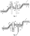
- the electric circuit shown comprises a flex circuit 1 which is a double-sided flex circuit having two flat printed electrical conductive layers 3, copper for example. These conductive layers 3 are superimposed and insulated from each other by a layer of medium planar dielectric resin 5, high thermal resistance, of polyimide type for example.
- the thickness of each of the conductive and insulating layers 5 is here equal to about 10 micrometers. Therefore, the thickness of the section of the flex circuit is about 30 micrometers, which gives it a bending and twisting ability.
- the width of the flex circuit is equal to 3 to 5 centimeters, which allows the transmission by the circuit of a current of 50 to 70 A for a current density passing in the flex below 10A / mm 2 .
- Such a current may indeed be that of an electrical component, for example that of a low to medium power component (not shown), as will be described below.
- the flex circuit 1 comprises two parts 7 forming a contact interface between the flex circuit and the power component. These contact parts 7 are hereinafter referred to as electric current diffusers.
- the component may comprise two pin-shaped cylindrical contact pins 9 (only represented).
- the electrical connection of these pins 9 with the flex circuit 1 is realized by means of the two electrical conductive parts or electric current diffusing devices 7.
- These devices for diffusing electric current 7 in fact connect each of the pins 9 of the electrical component to a respective conductive layer 3 of the flex circuit.
- These pins 9 are each arranged in a metallized hole or via 11 formed in the flex circuit, perpendicular to the surface of the latter.
- a lower via 11 on the flex circuit is thus formed for the left pin 9 (left in the figure) and an upper via 11 on the flex circuit is formed for the right pin.
- the electric current diffusers 7 are identical, each consisting of a good electrical conductor metal part, preferably copper, and having two contact portions 13, 15, each configured, respectively, to be applied in electrical contact with one another. pins 9 of the electrical component and with a conductive layer 3 of the flex circuit.
- the current diffuser part 7 here has the shape of a cylindrical sleeve 17 provided with a flat ring 19 at one of its ends, being shaped to come into contact with a pin pin 9 of the component by the cylindrical internal face 21 the sleeve and come into contact with a conductive layer 3 of the flex circuit by an outer face 23 of the ring.
- the first contact portion 13 is thus constituted by the cylindrical inner face 21 of the sleeve.
- the second contact portion 15 is then constituted by said outer face 23 of the ring.
- the contact junction of the two contact parts 13, 15, respectively with a pin 9 of the component and with a conductive layer 3 of the flex circuit, is obtained by a soldering joint of the parts.
- This brazing provides a conductive intermediate solder layer 25 between the contact portions facing each other, those 13 corresponding to the pin 9 of the component and those 15 corresponding to the conductive layer 3 of the flex circuit, this conductive intermediate layer 25 overflowing slightly outside each contact portion 13, 15.
- the current diffusing part 7 due to its massive appearance and the extent of its surface (of the part 15) in contact with the flex makes it possible to reduce the electrical current density in the contact zones, which is adjusted to a value less than 20 A / mm 2 , preferably between 4.5 and 5.5 A / mm 2 . relative to the contact surface of the contact portions 13, 15 with the component and the flex circuit, respectively. This feature reduces the heating of the contact links and makes the connection assembly more reliable.
- the massive nature of the current diffusers 7 gives them enough strength to constitute a possible mechanical connection point between the flex circuit and the component, allowing for example to mechanically link the flex circuit to the electrical component mounted knowing that the flex circuit can be deformed to fit the positioning of the component.
- the possible deformation of the flex circuit in flexion and torsion allows to give a certain freedom of positioning of the component on the flex circuit to adapt to the available space, especially in the context of an integrated assembly.
- the contact diffuser parts 7 may have another shape, see the figure 2 , than that described above.
- This diffuser part further comprises a contact ring 19 on its periphery, substantially in the upper part of the sleeve, this ring coming into contact with its lower face with the surface of the upper conductive layer 3 of the flex.
- the diffuser piece 7, on the right in the figure, comprises a first cylindrical portion of cylindrical portion contact 27, for example half cylindrical, coming into contact with an end portion of the pin 9 and a portion of its section. (Half), and the second contact portion is a flat ring 29 applied by its outer surface to the surface of the lower conductive layer 3 of the flex.
- the contact pins 9 are external to the flex circuit 1, being below it.
- the invention is not limited to the embodiments described and shown. It is for example possible to provide other forms for the contact parts of the current diffusers, which are adapted to the shape (complementary) of the contact elements of the electrical component to be mounted.
Landscapes
- Structure Of Printed Boards (AREA)
- Coupling Device And Connection With Printed Circuit (AREA)
- Contacts (AREA)
- Parts Printed On Printed Circuit Boards (AREA)
Applications Claiming Priority (2)
| Application Number | Priority Date | Filing Date | Title |
|---|---|---|---|
| FR1255117A FR2991514B1 (fr) | 2012-06-01 | 2012-06-01 | Circuit electrique comprenant un composant electrique et un circuit flex electrique relies ensemble par une piece conductrice electrique et utilisation de ce circuit |
| PCT/FR2013/051223 WO2013178957A1 (fr) | 2012-06-01 | 2013-05-30 | Circuit electrique pour l'interconnexion d'un composant electrique, tel qu'un composant de puissance |
Publications (2)
| Publication Number | Publication Date |
|---|---|
| EP2856563A1 EP2856563A1 (fr) | 2015-04-08 |
| EP2856563B1 true EP2856563B1 (fr) | 2016-05-25 |
Family
ID=46963816
Family Applications (1)
| Application Number | Title | Priority Date | Filing Date |
|---|---|---|---|
| EP13731378.9A Active EP2856563B1 (fr) | 2012-06-01 | 2013-05-30 | Circuit électrique pour l'interconnexion d'un composant électrique, tel qu'un composant de puissance |
Country Status (9)
| Country | Link |
|---|---|
| US (1) | US9350094B2 (https=) |
| EP (1) | EP2856563B1 (https=) |
| JP (1) | JP6235002B2 (https=) |
| CN (1) | CN104428955B (https=) |
| BR (1) | BR112014028758B1 (https=) |
| CA (1) | CA2872746C (https=) |
| FR (1) | FR2991514B1 (https=) |
| RU (1) | RU2631263C2 (https=) |
| WO (1) | WO2013178957A1 (https=) |
Families Citing this family (4)
| Publication number | Priority date | Publication date | Assignee | Title |
|---|---|---|---|---|
| US9972930B1 (en) * | 2017-01-16 | 2018-05-15 | Methode Electronics, Inc. | Transceiver module wit flex circuit |
| DE102020100364B4 (de) * | 2020-01-09 | 2022-04-21 | Semikron Elektronik Gmbh & Co. Kg | Leistungselektronische Baugruppe mit einem Substrat, einer Hülse und einem Kontaktstift und Verfahren zur Herstellung einer solchen Baugruppe |
| EP4205516A4 (en) | 2020-10-02 | 2024-08-28 | CelLink Corporation | Forming connections to flexible interconnect circuits |
| KR20230079161A (ko) | 2020-10-02 | 2023-06-05 | 셀링크 코포레이션 | 가요성 상호접속 회로를 연결하기 위한 방법 및 시스템 |
Family Cites Families (15)
| Publication number | Priority date | Publication date | Assignee | Title |
|---|---|---|---|---|
| US4595248A (en) * | 1983-04-21 | 1986-06-17 | Brown James C | Terminal block |
| US4530551A (en) * | 1984-01-12 | 1985-07-23 | Burroughs Corp. | Circuit change pin for printed wiring board |
| US4906198A (en) * | 1988-12-12 | 1990-03-06 | International Business Machines Corporation | Circuit board assembly and contact pin for use therein |
| US5277595A (en) * | 1992-06-29 | 1994-01-11 | E. I. Du Pont De Nemours And Company | Power receptacle for a daughterboard |
| JP3112868B2 (ja) * | 1997-09-12 | 2000-11-27 | 甲府日本電気株式会社 | 電子装置の給電装置 |
| JP3703423B2 (ja) * | 2001-10-18 | 2005-10-05 | ヒロセ電機株式会社 | フレキシブル回路基板接続装置 |
| US7025604B2 (en) * | 2003-03-31 | 2006-04-11 | Astec International Limited | High current output pin |
| DE102005013953A1 (de) | 2005-03-26 | 2006-09-28 | Jungheinrich Ag | Stromanschluß für eine Leistungs- und Steuereinheit eines batteriebetriebenen Flurförderzeugs |
| JP4613799B2 (ja) * | 2005-11-10 | 2011-01-19 | パナソニック電工株式会社 | 基板接続用コネクタ組立体 |
| DE102006004322A1 (de) * | 2006-01-31 | 2007-08-16 | Häusermann GmbH | Leiterplatte mit zusätzlichen funktionalen Elementen sowie Herstellverfahren und Anwendung |
| DE102008001557A1 (de) * | 2008-05-05 | 2009-11-12 | Robert Bosch Gmbh | Messerleisten-Kontaktierung über Zwischenleiterplatten |
| JP5142386B2 (ja) * | 2008-08-06 | 2013-02-13 | 日本航空電子工業株式会社 | コネクタ |
| RU92746U1 (ru) * | 2009-12-18 | 2010-03-27 | Федеральное государственное унитарное предприятие "Производственное объединение "Уральский оптико-механический завод" имени Э.С. Яламова" | Соединитель для печатных плат |
| DE102010039740A1 (de) * | 2010-08-25 | 2012-03-01 | Robert Bosch Gmbh | Kontaktelement zur Kontaktierung eines Schaltungsträgers, sowie Schaltungsträger mit einem Kontaktelement |
| RU112578U1 (ru) * | 2011-07-25 | 2012-01-10 | Открытое акционерное общество "Научно-производственный комплекс "ЭЛАРА" имени Г.А. Ильенко" (ОАО "ЭЛАРА") | Соединение гибкого печатного кабеля с жесткой печатной платой |
-
2012
- 2012-06-01 FR FR1255117A patent/FR2991514B1/fr active Active
-
2013
- 2013-05-30 US US14/402,181 patent/US9350094B2/en active Active
- 2013-05-30 JP JP2015514568A patent/JP6235002B2/ja not_active Expired - Fee Related
- 2013-05-30 WO PCT/FR2013/051223 patent/WO2013178957A1/fr not_active Ceased
- 2013-05-30 RU RU2014148979A patent/RU2631263C2/ru active
- 2013-05-30 BR BR112014028758-9A patent/BR112014028758B1/pt not_active IP Right Cessation
- 2013-05-30 EP EP13731378.9A patent/EP2856563B1/fr active Active
- 2013-05-30 CN CN201380027079.0A patent/CN104428955B/zh active Active
- 2013-05-30 CA CA2872746A patent/CA2872746C/fr not_active Expired - Fee Related
Non-Patent Citations (1)
| Title |
|---|
| None * |
Also Published As
| Publication number | Publication date |
|---|---|
| CN104428955A (zh) | 2015-03-18 |
| WO2013178957A1 (fr) | 2013-12-05 |
| JP6235002B2 (ja) | 2017-11-22 |
| CA2872746A1 (fr) | 2013-12-05 |
| FR2991514A1 (fr) | 2013-12-06 |
| US20150126049A1 (en) | 2015-05-07 |
| JP2015520492A (ja) | 2015-07-16 |
| EP2856563A1 (fr) | 2015-04-08 |
| RU2014148979A (ru) | 2016-08-10 |
| CN104428955B (zh) | 2017-08-04 |
| BR112014028758A2 (pt) | 2017-06-27 |
| CA2872746C (fr) | 2021-03-23 |
| BR112014028758A8 (pt) | 2018-04-03 |
| FR2991514B1 (fr) | 2016-01-29 |
| RU2631263C2 (ru) | 2017-09-20 |
| US9350094B2 (en) | 2016-05-24 |
| BR112014028758B1 (pt) | 2021-07-20 |
Similar Documents
| Publication | Publication Date | Title |
|---|---|---|
| EP2856563B1 (fr) | Circuit électrique pour l'interconnexion d'un composant électrique, tel qu'un composant de puissance | |
| US9538692B2 (en) | Integrated heat exchanger and power delivery system for high powered electronic modules | |
| EP2124238B1 (fr) | Dispositif de contact pour contacteur de forte puissance résistive | |
| EP3711104B1 (fr) | Bloc energetique constitue par un assemblage sans soudure d'une pluralite de cellules de batteries | |
| CN100403569C (zh) | 热电变换装置以及热电变换装置的制造方法 | |
| EP1047294A1 (fr) | Substrat métallique isolé pour circuits imprimés | |
| CA2239252A1 (fr) | Module electronique de puissance, et systeme electronique de puissance comprenant une pluralite dudit module | |
| EP1172026B1 (fr) | Module electronique de puissance et procede de fabrication d'un tel module | |
| US20100203378A1 (en) | Device providing electrical connection between electrochemical cells | |
| US20210100129A1 (en) | Power conversion device | |
| JP2023083614A (ja) | 熱電変換モジュール | |
| EP3078245A1 (fr) | Procede de fabrication d'un circuit imprime de puissance et circuit imprime de puissance obtenu par ce procede | |
| EP3966851B1 (fr) | Procede de fabrication d'un module electronique de puissance | |
| EP1569303B1 (fr) | Dispositif de retour d'alimentation électrique pour équipements avioniques | |
| EP2123137B1 (fr) | Carte electronique et aeronef la comportant | |
| EP1506575A2 (fr) | Assemblage de composants de puissance sur un circuit imprime ainsi qu un procede d obtention d un tel assemblage | |
| FR3116173A1 (fr) | Circuit électrique de puissance pour convertisseur de puissance électrique | |
| EP4295400A1 (fr) | Module électronique de puissance | |
| CN113039870A (zh) | 电路载体、(电力)电子组件和电驱动装置 | |
| CN104854964A (zh) | 用于多层电路载体的接触组件 | |
| FR3153719A1 (fr) | Ensemble comportant deux composants d’électronique de puissance et un interconnecteur | |
| CN114258188A (zh) | 电路板和用于检测电的接触元件的温度的方法 | |
| EP0637826A1 (fr) | Composant résistif de puissance, avec dispositif d'application sous pression sur un dissipateur thermique | |
| EP0426553A1 (fr) | Système de raccordement pour câble plat blindé | |
| FR2995495A1 (fr) | Dispositif electrique et compresseur electrique |
Legal Events
| Date | Code | Title | Description |
|---|---|---|---|
| PUAI | Public reference made under article 153(3) epc to a published international application that has entered the european phase |
Free format text: ORIGINAL CODE: 0009012 |
|
| 17P | Request for examination filed |
Effective date: 20141230 |
|
| AK | Designated contracting states |
Kind code of ref document: A1 Designated state(s): AL AT BE BG CH CY CZ DE DK EE ES FI FR GB GR HR HU IE IS IT LI LT LU LV MC MK MT NL NO PL PT RO RS SE SI SK SM TR |
|
| AX | Request for extension of the european patent |
Extension state: BA ME |
|
| RAP1 | Party data changed (applicant data changed or rights of an application transferred) |
Owner name: LABINAL POWER SYSTEMS |
|
| DAX | Request for extension of the european patent (deleted) | ||
| GRAP | Despatch of communication of intention to grant a patent |
Free format text: ORIGINAL CODE: EPIDOSNIGR1 |
|
| INTG | Intention to grant announced |
Effective date: 20160223 |
|
| GRAS | Grant fee paid |
Free format text: ORIGINAL CODE: EPIDOSNIGR3 |
|
| GRAA | (expected) grant |
Free format text: ORIGINAL CODE: 0009210 |
|
| REG | Reference to a national code |
Ref country code: FR Ref legal event code: PLFP Year of fee payment: 4 |
|
| AK | Designated contracting states |
Kind code of ref document: B1 Designated state(s): AL AT BE BG CH CY CZ DE DK EE ES FI FR GB GR HR HU IE IS IT LI LT LU LV MC MK MT NL NO PL PT RO RS SE SI SK SM TR |
|
| REG | Reference to a national code |
Ref country code: GB Ref legal event code: FG4D Free format text: NOT ENGLISH |
|
| REG | Reference to a national code |
Ref country code: CH Ref legal event code: EP |
|
| REG | Reference to a national code |
Ref country code: IE Ref legal event code: FG4D Free format text: LANGUAGE OF EP DOCUMENT: FRENCH Ref country code: AT Ref legal event code: REF Ref document number: 803010 Country of ref document: AT Kind code of ref document: T Effective date: 20160615 |
|
| REG | Reference to a national code |
Ref country code: DE Ref legal event code: R096 Ref document number: 602013008008 Country of ref document: DE |
|
| RAP2 | Party data changed (patent owner data changed or rights of a patent transferred) |
Owner name: SAFRAN ELECTRICAL & POWER |
|
| REG | Reference to a national code |
Ref country code: LT Ref legal event code: MG4D |
|
| REG | Reference to a national code |
Ref country code: NL Ref legal event code: MP Effective date: 20160525 |
|
| PG25 | Lapsed in a contracting state [announced via postgrant information from national office to epo] |
Ref country code: NL Free format text: LAPSE BECAUSE OF FAILURE TO SUBMIT A TRANSLATION OF THE DESCRIPTION OR TO PAY THE FEE WITHIN THE PRESCRIBED TIME-LIMIT Effective date: 20160525 Ref country code: FI Free format text: LAPSE BECAUSE OF FAILURE TO SUBMIT A TRANSLATION OF THE DESCRIPTION OR TO PAY THE FEE WITHIN THE PRESCRIBED TIME-LIMIT Effective date: 20160525 Ref country code: NO Free format text: LAPSE BECAUSE OF FAILURE TO SUBMIT A TRANSLATION OF THE DESCRIPTION OR TO PAY THE FEE WITHIN THE PRESCRIBED TIME-LIMIT Effective date: 20160825 Ref country code: LT Free format text: LAPSE BECAUSE OF FAILURE TO SUBMIT A TRANSLATION OF THE DESCRIPTION OR TO PAY THE FEE WITHIN THE PRESCRIBED TIME-LIMIT Effective date: 20160525 |
|
| REG | Reference to a national code |
Ref country code: AT Ref legal event code: MK05 Ref document number: 803010 Country of ref document: AT Kind code of ref document: T Effective date: 20160525 |
|
| PG25 | Lapsed in a contracting state [announced via postgrant information from national office to epo] |
Ref country code: GR Free format text: LAPSE BECAUSE OF FAILURE TO SUBMIT A TRANSLATION OF THE DESCRIPTION OR TO PAY THE FEE WITHIN THE PRESCRIBED TIME-LIMIT Effective date: 20160826 Ref country code: ES Free format text: LAPSE BECAUSE OF FAILURE TO SUBMIT A TRANSLATION OF THE DESCRIPTION OR TO PAY THE FEE WITHIN THE PRESCRIBED TIME-LIMIT Effective date: 20160525 Ref country code: SE Free format text: LAPSE BECAUSE OF FAILURE TO SUBMIT A TRANSLATION OF THE DESCRIPTION OR TO PAY THE FEE WITHIN THE PRESCRIBED TIME-LIMIT Effective date: 20160525 Ref country code: PT Free format text: LAPSE BECAUSE OF FAILURE TO SUBMIT A TRANSLATION OF THE DESCRIPTION OR TO PAY THE FEE WITHIN THE PRESCRIBED TIME-LIMIT Effective date: 20160926 Ref country code: LV Free format text: LAPSE BECAUSE OF FAILURE TO SUBMIT A TRANSLATION OF THE DESCRIPTION OR TO PAY THE FEE WITHIN THE PRESCRIBED TIME-LIMIT Effective date: 20160525 Ref country code: RS Free format text: LAPSE BECAUSE OF FAILURE TO SUBMIT A TRANSLATION OF THE DESCRIPTION OR TO PAY THE FEE WITHIN THE PRESCRIBED TIME-LIMIT Effective date: 20160525 |
|
| PG25 | Lapsed in a contracting state [announced via postgrant information from national office to epo] |
Ref country code: BE Free format text: LAPSE BECAUSE OF NON-PAYMENT OF DUE FEES Effective date: 20160531 |
|
| REG | Reference to a national code |
Ref country code: CH Ref legal event code: PL |
|
| PG25 | Lapsed in a contracting state [announced via postgrant information from national office to epo] |
Ref country code: LI Free format text: LAPSE BECAUSE OF NON-PAYMENT OF DUE FEES Effective date: 20160531 Ref country code: DK Free format text: LAPSE BECAUSE OF FAILURE TO SUBMIT A TRANSLATION OF THE DESCRIPTION OR TO PAY THE FEE WITHIN THE PRESCRIBED TIME-LIMIT Effective date: 20160525 Ref country code: EE Free format text: LAPSE BECAUSE OF FAILURE TO SUBMIT A TRANSLATION OF THE DESCRIPTION OR TO PAY THE FEE WITHIN THE PRESCRIBED TIME-LIMIT Effective date: 20160525 Ref country code: CZ Free format text: LAPSE BECAUSE OF FAILURE TO SUBMIT A TRANSLATION OF THE DESCRIPTION OR TO PAY THE FEE WITHIN THE PRESCRIBED TIME-LIMIT Effective date: 20160525 Ref country code: CH Free format text: LAPSE BECAUSE OF NON-PAYMENT OF DUE FEES Effective date: 20160531 Ref country code: RO Free format text: LAPSE BECAUSE OF FAILURE TO SUBMIT A TRANSLATION OF THE DESCRIPTION OR TO PAY THE FEE WITHIN THE PRESCRIBED TIME-LIMIT Effective date: 20160525 Ref country code: SK Free format text: LAPSE BECAUSE OF FAILURE TO SUBMIT A TRANSLATION OF THE DESCRIPTION OR TO PAY THE FEE WITHIN THE PRESCRIBED TIME-LIMIT Effective date: 20160525 |
|
| REG | Reference to a national code |
Ref country code: IE Ref legal event code: MM4A |
|
| PG25 | Lapsed in a contracting state [announced via postgrant information from national office to epo] |
Ref country code: AT Free format text: LAPSE BECAUSE OF FAILURE TO SUBMIT A TRANSLATION OF THE DESCRIPTION OR TO PAY THE FEE WITHIN THE PRESCRIBED TIME-LIMIT Effective date: 20160525 Ref country code: SM Free format text: LAPSE BECAUSE OF FAILURE TO SUBMIT A TRANSLATION OF THE DESCRIPTION OR TO PAY THE FEE WITHIN THE PRESCRIBED TIME-LIMIT Effective date: 20160525 Ref country code: PL Free format text: LAPSE BECAUSE OF FAILURE TO SUBMIT A TRANSLATION OF THE DESCRIPTION OR TO PAY THE FEE WITHIN THE PRESCRIBED TIME-LIMIT Effective date: 20160525 |
|
| REG | Reference to a national code |
Ref country code: DE Ref legal event code: R097 Ref document number: 602013008008 Country of ref document: DE |
|
| PG25 | Lapsed in a contracting state [announced via postgrant information from national office to epo] |
Ref country code: MC Free format text: LAPSE BECAUSE OF FAILURE TO SUBMIT A TRANSLATION OF THE DESCRIPTION OR TO PAY THE FEE WITHIN THE PRESCRIBED TIME-LIMIT Effective date: 20160525 |
|
| PLBE | No opposition filed within time limit |
Free format text: ORIGINAL CODE: 0009261 |
|
| STAA | Information on the status of an ep patent application or granted ep patent |
Free format text: STATUS: NO OPPOSITION FILED WITHIN TIME LIMIT |
|
| REG | Reference to a national code |
Ref country code: FR Ref legal event code: PLFP Year of fee payment: 5 |
|
| 26N | No opposition filed |
Effective date: 20170228 |
|
| PG25 | Lapsed in a contracting state [announced via postgrant information from national office to epo] |
Ref country code: SI Free format text: LAPSE BECAUSE OF FAILURE TO SUBMIT A TRANSLATION OF THE DESCRIPTION OR TO PAY THE FEE WITHIN THE PRESCRIBED TIME-LIMIT Effective date: 20160525 Ref country code: IE Free format text: LAPSE BECAUSE OF NON-PAYMENT OF DUE FEES Effective date: 20160530 |
|
| PG25 | Lapsed in a contracting state [announced via postgrant information from national office to epo] |
Ref country code: IT Free format text: LAPSE BECAUSE OF FAILURE TO SUBMIT A TRANSLATION OF THE DESCRIPTION OR TO PAY THE FEE WITHIN THE PRESCRIBED TIME-LIMIT Effective date: 20160525 |
|
| REG | Reference to a national code |
Ref country code: FR Ref legal event code: PLFP Year of fee payment: 6 |
|
| PG25 | Lapsed in a contracting state [announced via postgrant information from national office to epo] |
Ref country code: HU Free format text: LAPSE BECAUSE OF FAILURE TO SUBMIT A TRANSLATION OF THE DESCRIPTION OR TO PAY THE FEE WITHIN THE PRESCRIBED TIME-LIMIT; INVALID AB INITIO Effective date: 20130530 |
|
| PG25 | Lapsed in a contracting state [announced via postgrant information from national office to epo] |
Ref country code: LU Free format text: LAPSE BECAUSE OF NON-PAYMENT OF DUE FEES Effective date: 20160530 Ref country code: CY Free format text: LAPSE BECAUSE OF FAILURE TO SUBMIT A TRANSLATION OF THE DESCRIPTION OR TO PAY THE FEE WITHIN THE PRESCRIBED TIME-LIMIT Effective date: 20160525 Ref country code: MK Free format text: LAPSE BECAUSE OF FAILURE TO SUBMIT A TRANSLATION OF THE DESCRIPTION OR TO PAY THE FEE WITHIN THE PRESCRIBED TIME-LIMIT Effective date: 20160525 Ref country code: IS Free format text: LAPSE BECAUSE OF FAILURE TO SUBMIT A TRANSLATION OF THE DESCRIPTION OR TO PAY THE FEE WITHIN THE PRESCRIBED TIME-LIMIT Effective date: 20160525 Ref country code: MT Free format text: LAPSE BECAUSE OF FAILURE TO SUBMIT A TRANSLATION OF THE DESCRIPTION OR TO PAY THE FEE WITHIN THE PRESCRIBED TIME-LIMIT Effective date: 20160525 Ref country code: HR Free format text: LAPSE BECAUSE OF FAILURE TO SUBMIT A TRANSLATION OF THE DESCRIPTION OR TO PAY THE FEE WITHIN THE PRESCRIBED TIME-LIMIT Effective date: 20160525 |
|
| PG25 | Lapsed in a contracting state [announced via postgrant information from national office to epo] |
Ref country code: BG Free format text: LAPSE BECAUSE OF FAILURE TO SUBMIT A TRANSLATION OF THE DESCRIPTION OR TO PAY THE FEE WITHIN THE PRESCRIBED TIME-LIMIT Effective date: 20160525 |
|
| PG25 | Lapsed in a contracting state [announced via postgrant information from national office to epo] |
Ref country code: AL Free format text: LAPSE BECAUSE OF FAILURE TO SUBMIT A TRANSLATION OF THE DESCRIPTION OR TO PAY THE FEE WITHIN THE PRESCRIBED TIME-LIMIT Effective date: 20160525 Ref country code: TR Free format text: LAPSE BECAUSE OF FAILURE TO SUBMIT A TRANSLATION OF THE DESCRIPTION OR TO PAY THE FEE WITHIN THE PRESCRIBED TIME-LIMIT Effective date: 20160525 |
|
| PGFP | Annual fee paid to national office [announced via postgrant information from national office to epo] |
Ref country code: DE Payment date: 20210421 Year of fee payment: 9 |
|
| REG | Reference to a national code |
Ref country code: DE Ref legal event code: R119 Ref document number: 602013008008 Country of ref document: DE |
|
| PG25 | Lapsed in a contracting state [announced via postgrant information from national office to epo] |
Ref country code: DE Free format text: LAPSE BECAUSE OF NON-PAYMENT OF DUE FEES Effective date: 20221201 |
|
| PGFP | Annual fee paid to national office [announced via postgrant information from national office to epo] |
Ref country code: GB Payment date: 20250527 Year of fee payment: 13 |
|
| PGFP | Annual fee paid to national office [announced via postgrant information from national office to epo] |
Ref country code: FR Payment date: 20250526 Year of fee payment: 13 |