EP2854170A1 - A structure for a heat transfer interface and method of manufacturing the same - Google Patents
A structure for a heat transfer interface and method of manufacturing the same Download PDFInfo
- Publication number
- EP2854170A1 EP2854170A1 EP20130306340 EP13306340A EP2854170A1 EP 2854170 A1 EP2854170 A1 EP 2854170A1 EP 20130306340 EP20130306340 EP 20130306340 EP 13306340 A EP13306340 A EP 13306340A EP 2854170 A1 EP2854170 A1 EP 2854170A1
- Authority
- EP
- European Patent Office
- Prior art keywords
- heat transfer
- interface structure
- transfer interface
- raised
- raised features
- Prior art date
- Legal status (The legal status is an assumption and is not a legal conclusion. Google has not performed a legal analysis and makes no representation as to the accuracy of the status listed.)
- Granted
Links
Images


Classifications
-
- H—ELECTRICITY
- H05—ELECTRIC TECHNIQUES NOT OTHERWISE PROVIDED FOR
- H05K—PRINTED CIRCUITS; CASINGS OR CONSTRUCTIONAL DETAILS OF ELECTRIC APPARATUS; MANUFACTURE OF ASSEMBLAGES OF ELECTRICAL COMPONENTS
- H05K7/00—Constructional details common to different types of electric apparatus
- H05K7/20—Modifications to facilitate cooling, ventilating, or heating
- H05K7/2039—Modifications to facilitate cooling, ventilating, or heating characterised by the heat transfer by conduction from the heat generating element to a dissipating body
-
- B—PERFORMING OPERATIONS; TRANSPORTING
- B21—MECHANICAL METAL-WORKING WITHOUT ESSENTIALLY REMOVING MATERIAL; PUNCHING METAL
- B21D—WORKING OR PROCESSING OF SHEET METAL OR METAL TUBES, RODS OR PROFILES WITHOUT ESSENTIALLY REMOVING MATERIAL; PUNCHING METAL
- B21D13/00—Corrugating sheet metal, rods or profiles; Bending sheet metal, rods or profiles into wave form
- B21D13/02—Corrugating sheet metal, rods or profiles; Bending sheet metal, rods or profiles into wave form by pressing
-
- B—PERFORMING OPERATIONS; TRANSPORTING
- B21—MECHANICAL METAL-WORKING WITHOUT ESSENTIALLY REMOVING MATERIAL; PUNCHING METAL
- B21D—WORKING OR PROCESSING OF SHEET METAL OR METAL TUBES, RODS OR PROFILES WITHOUT ESSENTIALLY REMOVING MATERIAL; PUNCHING METAL
- B21D33/00—Special measures in connection with working metal foils, e.g. gold foils
-
- B—PERFORMING OPERATIONS; TRANSPORTING
- B21—MECHANICAL METAL-WORKING WITHOUT ESSENTIALLY REMOVING MATERIAL; PUNCHING METAL
- B21D—WORKING OR PROCESSING OF SHEET METAL OR METAL TUBES, RODS OR PROFILES WITHOUT ESSENTIALLY REMOVING MATERIAL; PUNCHING METAL
- B21D53/00—Making other particular articles
- B21D53/02—Making other particular articles heat exchangers or parts thereof, e.g. radiators, condensers fins, headers
- B21D53/04—Making other particular articles heat exchangers or parts thereof, e.g. radiators, condensers fins, headers of sheet metal
-
- H—ELECTRICITY
- H10—SEMICONDUCTOR DEVICES; ELECTRIC SOLID-STATE DEVICES NOT OTHERWISE PROVIDED FOR
- H10W—GENERIC PACKAGES, INTERCONNECTIONS, CONNECTORS OR OTHER CONSTRUCTIONAL DETAILS OF DEVICES COVERED BY CLASS H10
- H10W40/00—Arrangements for thermal protection or thermal control
- H10W40/20—Arrangements for cooling
- H10W40/22—Arrangements for cooling characterised by their shape, e.g. having conical or cylindrical projections
-
- H—ELECTRICITY
- H10—SEMICONDUCTOR DEVICES; ELECTRIC SOLID-STATE DEVICES NOT OTHERWISE PROVIDED FOR
- H10W—GENERIC PACKAGES, INTERCONNECTIONS, CONNECTORS OR OTHER CONSTRUCTIONAL DETAILS OF DEVICES COVERED BY CLASS H10
- H10W40/00—Arrangements for thermal protection or thermal control
- H10W40/20—Arrangements for cooling
- H10W40/25—Arrangements for cooling characterised by their materials
- H10W40/255—Arrangements for cooling characterised by their materials having a laminate or multilayered structure, e.g. direct bond copper [DBC] ceramic substrates
-
- H—ELECTRICITY
- H10—SEMICONDUCTOR DEVICES; ELECTRIC SOLID-STATE DEVICES NOT OTHERWISE PROVIDED FOR
- H10W—GENERIC PACKAGES, INTERCONNECTIONS, CONNECTORS OR OTHER CONSTRUCTIONAL DETAILS OF DEVICES COVERED BY CLASS H10
- H10W40/00—Arrangements for thermal protection or thermal control
- H10W40/20—Arrangements for cooling
- H10W40/25—Arrangements for cooling characterised by their materials
- H10W40/258—Metallic materials
-
- H—ELECTRICITY
- H10—SEMICONDUCTOR DEVICES; ELECTRIC SOLID-STATE DEVICES NOT OTHERWISE PROVIDED FOR
- H10W—GENERIC PACKAGES, INTERCONNECTIONS, CONNECTORS OR OTHER CONSTRUCTIONAL DETAILS OF DEVICES COVERED BY CLASS H10
- H10W40/00—Arrangements for thermal protection or thermal control
- H10W40/70—Fillings or auxiliary members in containers or in encapsulations for thermal protection or control
-
- H—ELECTRICITY
- H10—SEMICONDUCTOR DEVICES; ELECTRIC SOLID-STATE DEVICES NOT OTHERWISE PROVIDED FOR
- H10W—GENERIC PACKAGES, INTERCONNECTIONS, CONNECTORS OR OTHER CONSTRUCTIONAL DETAILS OF DEVICES COVERED BY CLASS H10
- H10W40/00—Arrangements for thermal protection or thermal control
- H10W40/70—Fillings or auxiliary members in containers or in encapsulations for thermal protection or control
- H10W40/77—Auxiliary members characterised by their shape
-
- H—ELECTRICITY
- H10—SEMICONDUCTOR DEVICES; ELECTRIC SOLID-STATE DEVICES NOT OTHERWISE PROVIDED FOR
- H10W—GENERIC PACKAGES, INTERCONNECTIONS, CONNECTORS OR OTHER CONSTRUCTIONAL DETAILS OF DEVICES COVERED BY CLASS H10
- H10W70/00—Package substrates; Interposers; Redistribution layers [RDL]
- H10W70/01—Manufacture or treatment
- H10W70/02—Manufacture or treatment of conductive package substrates serving as an interconnection, e.g. of metal plates
- H10W70/027—Mechanical treatments, e.g. deforming, punching or cutting
-
- F—MECHANICAL ENGINEERING; LIGHTING; HEATING; WEAPONS; BLASTING
- F28—HEAT EXCHANGE IN GENERAL
- F28F—DETAILS OF HEAT-EXCHANGE AND HEAT-TRANSFER APPARATUS, OF GENERAL APPLICATION
- F28F13/00—Arrangements for modifying heat-transfer, e.g. increasing, decreasing
- F28F2013/005—Thermal joints
- F28F2013/006—Heat conductive materials
Definitions
- the present disclosure relates to heat transfer devices.
- Electric and electronic components typically generate heat during operation.
- a heat dissipating components such as a heat sink which is typically positioned in physical contact with the heat generating component to absorb and dissipate heat from the latter.
- a heat dissipating component such as a heat sink
- the temperature difference across the interface of the parts may be appreciable.
- This temperature drop is typically attributed to the thermal contact resistance due to surface roughness effects, as such surface roughness effects give rise to interstitial air voids between the surfaces of the two components being joined together. For mating surfaces that appear relatively smooth and flat, the contact made between these two parts typically occurs at relatively few points.
- the voids between these points of contact are often filled with some type of fluid-typically air.
- fluid-typically air there are two paths for heat transfer, one being thermal conduction through the solid components at their points of contact and the other being thermal conduction through the interfacial layer of air, which is a relatively poor conductor.
- the poor physical contact may also give rise to an excessively high electrical contact resistance which may also be a problem in certain systems where electrical conduction or grounding through contacting joints is important.
- One embodiment is a thermally conductive heat transfer interface structure comprising a substrate having a first surface and a second surface and a plurality of raised features formed on at least one of the first surface and the second surface of the substrate, the raised features being deformable under a compressive force, wherein some of the raised features have an opening at a respective end portion thereof.
- the heat transfer interface structure has the form of a deformable sheet.
- a heat transfer interface structure comprising a substrate having a first surface and a second surface and a plurality of raised features formed on at least one of the first surface and the second surface of the substrate, the raised features being deformable under a compressive force, wherein a raised feature has an opening at an end portion thereof.
- the raised features are arranged in the form of a two-dimensional array.
- the opening is at a truncated end portion of the raised feature.
- the raised feature is configured to bend or buckle under compression.
- a plurality of raised features has the form of an array.
- a raised feature is configured to adopt a compressed shape under the compressive force such that the resulting compressed shape is capable of conducting a higher amount of heat than a shape of the raised feature before compression.
- a raised feature having an opening at an end portion thereof is capable of allowing a flow of a liquid material during compression.
- the liquid material is grease or adhesive.
- the heat transfer interface structure is of a material including a malleable and conductive metals or alloys.
- the heat transfer interface structure is made of tin.
- the heat transfer interface structure further comprises coating disposed over the heat transfer interface structure, said coating being configured to alter electrical, thermal or chemical characteristics of the heat transfer interface structure.
- the coating of heat transfer interface structure is configured to provide compliance to the heat transfer interface structure.
- the coating of heat transfer interface structure is an electrical insulator.
- Another embodiment is an apparatus comprising an electric component capable of generating heat, a heat dissipater component and a heat transfer interface structure as featured herein, said heat transfer interfaced structure being located between the electric component and the dissipater component.
- Another embodiment is a method, comprising:
- the deformable sheet is made of tin and the compressive force is above about 0.5 MPa.
- the method further comprises applying an interpenetrating liquid during compression, such liquid being capable of flowing between the dies and though the heat transfer interface structure to eliminate air.
- thermal interface materials are often composites of thermally conductive particles dispersed in a thermally insulating organic matrix (e.g., adhesive or grease).
- the thermal conductivity of such composites is limited by the relatively low concentration of particles, as often needed to assure proper viscosity, and by the thermal resistance of particle-particle contacts. Additionally, air-filled voids, which have poor thermal conductivity, can accumulate in the organic matrix, thereby decreasing the overall thermal conductivity of the TIM.
- Soft metals such as Indium, or other soft materials, such as graphite, are also sometimes used as thermal interface materials. Although the thermal conductivity of these materials is higher than the composite materials, they have limited ability to comply with non-planar or irregular surfaces. Some of these soft materials are susceptible to corrosion, and, can have low melting points. All of these limitations can restrict reliability, applicability and assembly options.
- Figure 1 shows a simplified example of a known interface structure 100. Although the drawing shown in figure 1 is similar to an embodiment as disclosed in the above-referenced document, figure 1 is only provided for illustration purposes and a better understanding of the present disclosure and is not be construed to necessarily include all the features, limitations and/or variants of embodiments of the referenced US20090315173 .
- the interface structure 100 of figure 1 is intended for use as a heat transfer interface structure between components 130 and 132 having respective interface surfaces 125, 127.
- the interface surfaces 125, 127 have surface non-uniformities (or irregularities or roughnesses).
- the structure 100 comprises a substrate 110 having raised features 120.
- the raised features 120 are designed to physically contact both surfaces 125, 127 regardless of whether the surfaces 125, 127 are coplanar or whether one or both or the surfaces 125, 127 are curved or otherwise non-planar.
- the raised features 120 may be metallic and deformable and configured to be compressed in at least one dimension as compared to a pre-deformed shape. Compression in the at least one dimension can occur by bending or buckling of the shape of the raised features, or by other modes of changing the shape of the raised features.
- the direction of compression may be in the direction of arrow A1 or A2 or both.
- the raised features 120 may be located, and in some cases formed directly, on one or more surfaces of a substrate. As shown in the example of figure 1 the raised features 120 are located on both of the surfaces of a first side and an opposite second side of the planar substrate 100. In some cases, the substrate itself is a deformable metallic substrate.
- FIG. 2 is an exemplary schematic representation of a heat transfer interface structure 200 (herein also referred to as interface structure) according to some embodiments.
- the interface structure 200 comprises a substrate 210 and a plurality of raised features 220.
- the raised features 220 are preferably hollow and may be located on both of the surfaces of a first side (e.g. upper side of the structure of figure 2 shown by arrow UP) and an opposite second side (e.g. lower side of the structure of figure 2 which is not visible in the figure), or they may located on only one side thereof.
- the term “raised” is to be understood to refer not only to the features emerging upward from the surface of the substrate 210 but also the features emerging downward therefrom.
- a raised feature 220 has a base portion 222 which is the portion proximate to the body of the substrate 210 and an end portion 223 opposite to the base portion and being at a certain distance, or at a certain height, from the substrate 210.
- the raised features 220 are provided in the form of a two-dimensional array (e.g. length by width relative to the surface of the substrate 210) comprising a continuous plurality of such raised features.
- a raised feature 220 has an opening 230 at the end portion 223 thereof.
- the opening is made by truncating the end portion 223 of the raised feature (i.e. the end portion is cut off transversely with respect to the height of the raised feature).
- the raised features 220 are shown in the form of truncated domes; however other shapes such as, but not limited to, truncated cones or truncated multi-sided pyramids may also be made.
- the proposed shape for the raised features provides certain advantages as compared to the shape of the known raised features which do not have such openings incorporated, because it reduces the stiffness of the features thus presenting less resistance to the compression and flow of metal as the entire structure is compressed. Indeed a raised feature with an opening 230 may bend or buckle with a relatively lower pressure needed to be exerted thereupon (as compared to one without such opening).
- Raised features 220 with openings 230 may be provided in an array, as shown in figure 2 , comprising a plurality of such features positioned on the substrate 210 either randomly or periodically or according to any suitable pattern. Such array may significantly reduce the stress required for the material to conform to surface irregularities and thus provide a lower thermal contact resistance compared to known structures of raised features without openings 230.
- FIG 3 an exemplary schematic representation of the heat transfer interface structure of figure 2 is provided after such structure has undergone a compression.
- like elements have been given like reference numerals as those of figure 2 .
- the various elements of the structure have undergone deformation. It is readily observable that the raised features have undergone large-scale compressive deformation including bending and buckling modes resulting in relatively more flattened structures that form a continuous path between the assembled bodies, not shown in the figure (e.g. an electronic component and a heat sink). Such flattened structures may include areas that may come in intimate contact with the compressing surfaces.
- the raised structure 220-1 of figure may be considered in which the end portion 223-1 is shown to have been compressed, e.g. bent or buckled, toward the base portion 222-1 thereby resulting in a relatively more flattened structure as compared to known structures.
- the openings of the raised features in the present embodiment therefore allow for obtaining a highly effective thermal and electrical path between the mating components.
- the interface structure may be manufactured starting from a deformable and preferably flat sheet 410, such as a metal foil.
- the material of the sheet is chosen so as to posses the heat transfer, electrical and chemical characteristics required for the specific design and application.
- thermal conductivity For the sake of clarity with respect to the use of the term heat transfer characteristics, or said in other words, thermal conductivity, as used herein, the following clarification is provided.
- many materials, and even from a pure theoretical standpoint any material may be considered to be thermally conductive (thus having heat transfer capabilities) as each material has a certain level of thermal conductivity, even if in some cases such level is very low.
- a person skilled in the related art would be able to distinguish a material which is considered in the art as thermally conductive from one which is not so considered, such as for example a thermal insulator.
- any material having a thermal conductivity greater than about 1 W/mK may be considered as a thermally conductive material.
- any material having a thermal conductivity of less than about 1 W/mK may be considered as thermally non-conductive.
- a thermal conductivity greater than 100W/mK may be considered as a high thermal conductivity value and one within the range of 1-100W/mK may be considered as an acceptable value.
- the deformable sheet 410 is then placed between two dies 420 and 430 as schematically shown in figure 4 .
- the dies 420 and 430 have respective projections 421 and 431 and cavities 422 and 432 provided on their respective surfaces. It is to be noted that while the projections on one die point in one direction (e.g. projections 421 are shown pointing upward in the figure), the projections on the other (opposite) die point in the opposite direction (projections 431 point downward).
- the dies are then moved toward each other with sufficient force so as to compress and stamp the deformable sheet 410 placed between them.
- the projections 421, 431 and the cavities 422, 432 are configured such that a projection has matching shape and dimensions with a cavity in such a manner that when the two dies compress on the deformable sheet 410, a projection nests within a corresponding opposite cavity while it is deforming the deformable sheet in-between so as to shape it substantially according to the shape of the projection-cavity nested pair.
- the projections 421, 431 of the dies "punch through” and extrude the deformable sheet 410 to create the raised features, together with the corresponding opening on each raised feature, on deformable sheet 410, thereby producing the interface structure100 as illustrated in figure 3 .
- This manufacturing process not only facilitates the production of desirable interface material geometries, but also it is amenable to high-volume, low-cost fabrication of the interface structure.
- the dies 420 and 430 may be fabricated from a range of materials using various manufacturing techniques known by those skilled in the related art.
- the dies shown in the embodiment of figure 4 may be fabricated using a 3D printed polymer.
- Some materials suitable for the interface structure may include a range of malleable and conducting pure metals or alloys.
- One example is tin due to its low yield strength and reasonably high thermal and electrical conductivity.
- assembly pressures or chemical considerations stiffer, higher conductivity or chemically alternative metals or alloys may be desirable.
- applying pressure above 0.5 MPa provides a structured tin interface material which may demonstrate relatively high effective thermal conductivity and low thermal resistance than a graphite pad. Additionally, due to the large deformation range of this material, it may exhibit greater compliance over a range of pressures. Finally, due to the metallic nature of the tin interface material, it exhibits significantly lower electrical resistance. The aggregated effect of these factors results in significant performance improvements of the present embodiment using tin material for the interface structure material over some commercially available graphite pads.
- the material of the interface structure may initially comprise one or more layers of additional material (in the form of a sandwich).
- a further possibility is the use of overlaid material coatings to significantly alter the electrical, thermal and/or chemical response or performance of the interface material.
- Such coating may be primarily metallic, including but not limited to Gold (Au), Silver (Ag), Copper (Cu), Platinum (Pt), Palladium (Pa), Chrome (Cr), Zinc (Zn) Tin (Sn), Nickel (Ni) or Rhodium (Rh).
- the coating materials may be pure metals, metal oxides, or alloys containing a mixture of metallic materials, such as Gold Palladium.
- a soft metal may be coated with a conductive material (e.g. gold) that is resistant to oxidation and that lowers the electrical contact resistance between mating surfaces.
- the effect of sputter coating an additional layer of gold on the above embodiment using tin material may offer significant decrease in the electrical resistance over an un-coated interface material.
- the addition of an alloying over-layer may serve to seal the surface from subsequent oxidation, allowing a longer service lifetime.
- materials with higher levels of ductility may be used such as indium, tin, gallium or lead thereby increasing its capabilities in filling the gaps during compression and allowing it to form a tighter seal when bonded or compressed between layers in its application.
- the electrical conductivity may be desirable to limit the electrical conductivity while maintaining the thermal contact resistance.
- electrically insulative coatings such as polymers may be employed to obtain the desired result.
- Polymer materials are typically good electrical insulators and can be applied in thin, continuous coatings that are compliant.
- the dielectric coating could be applied either before or after stamping. Applying the coating before stamping is preferred as it may be easier and less expensive to achieve while a variety of coating techniques may be used.
- the dielectric layer may preferably be applied after the stamping operation to insure that the exposed surface edges generated during compression and punching are coated.
- One example of an effective approach is to coat the punched film using the polymer Parylene. This polymer dielectric may be deposited from the gas phase insuring conformal coating of uniform thickness over all exposed surfaces. In order to perform the coating process, use may be made of commercially available coating equipment.
- Such coatings may comprise just one additional layer, or several layers in a sandwich-type arrangement.
- the interfaces between the layers may be discrete and well-defined, or they may consist of inter-metallic layers with have a gradual change in the composition and morphology of the material.
- the coatings may be applied by a number of methods including, but not limited to: in-situ chemical oxidation, by sputter coating using a DC current, by magneto-resistance, by electroplating or electroless plating in a plating bath, or by vapor deposition using metal organic pre-cursors, physical vapors or plasma enhanced methods.
- the compressible solid interface structure may also be used in combination with an interpenetrating continuous phase of grease or adhesive to further improve the thermal, electrical or mechanical properties of the material upon compression.
- the raised features allow the flow of a fluid so as to fill gaps which may be formed during such compressions.
- the external clamping or assembly pressure may be removed and the thermal and electrical transport capabilities of the interface material would be maintained by the bonding effect of the adhesive.
- not all the raised features actually close the respective opening, thereby leaving some areas on the structure with openings. This array of opening permits grease, or adhesive, to flow evenly between the upper and lower interfaces thereby eliminating trapped air and forming an interface with improved thermal performance and, in the case of the adhesive, improved mechanical bond strength.
- the array of openings may also permit the grease or adhesive to flow between upper and lower surfaces of the interface structure forming a uniform thickness of material without significantly increasing the applied stress required for assembly.
- the proposed solution therefore offers improved thermal and electrical performance over conventional interface materials. Additionally, the manufacturing technique described herein is a low-cost alternative to conventional interface techniques. The addition of alternative metallic coatings to the interface material further improves its electrical properties making it a desirable solution for thermal and electrical interface applications.
Landscapes
- Engineering & Computer Science (AREA)
- Mechanical Engineering (AREA)
- Physics & Mathematics (AREA)
- Thermal Sciences (AREA)
- Microelectronics & Electronic Packaging (AREA)
- Cooling Or The Like Of Semiconductors Or Solid State Devices (AREA)
- Cooling Or The Like Of Electrical Apparatus (AREA)
- Chemical & Material Sciences (AREA)
- Ceramic Engineering (AREA)
Abstract
Description
- The present disclosure relates to heat transfer devices.
- Electric and electronic components typically generate heat during operation. In order to reduce the heat, use is often made of a heat dissipating components such as a heat sink which is typically positioned in physical contact with the heat generating component to absorb and dissipate heat from the latter. However when heat is conducted between two components (e.g. an IC and a heat sink) the temperature difference across the interface of the parts may be appreciable. This temperature drop is typically attributed to the thermal contact resistance due to surface roughness effects, as such surface roughness effects give rise to interstitial air voids between the surfaces of the two components being joined together. For mating surfaces that appear relatively smooth and flat, the contact made between these two parts typically occurs at relatively few points. The voids between these points of contact are often filled with some type of fluid-typically air. In this situation, there are two paths for heat transfer, one being thermal conduction through the solid components at their points of contact and the other being thermal conduction through the interfacial layer of air, which is a relatively poor conductor. Similarly, the poor physical contact may also give rise to an excessively high electrical contact resistance which may also be a problem in certain systems where electrical conduction or grounding through contacting joints is important.
- As a remedy to improve heat transfer between the two components one known approach is to replace the air with a more conductive thermal interface material (TIM), thereby improving the path for heat transfer between the two components
- One embodiment is a thermally conductive heat transfer interface structure comprising a substrate having a first surface and a second surface and a plurality of raised features formed on at least one of the first surface and the second surface of the substrate, the raised features being deformable under a compressive force, wherein some of the raised features have an opening at a respective end portion thereof.
- According to some specific embodiments, the heat transfer interface structure has the form of a deformable sheet.
a heat transfer interface structure comprising a substrate having a first surface and a second surface and a plurality of raised features formed on at least one of the first surface and the second surface of the substrate, the raised features being deformable under a compressive force, wherein a raised feature has an opening at an end portion thereof. - According to some specific embodiments, the raised features are arranged in the form of a two-dimensional array.
- According to some specific embodiments, the opening is at a truncated end portion of the raised feature.
- According to some specific embodiments, the raised feature is configured to bend or buckle under compression.
- According to some specific embodiments, a plurality of raised features has the form of an array.
- According to some specific embodiments, a raised feature is configured to adopt a compressed shape under the compressive force such that the resulting compressed shape is capable of conducting a higher amount of heat than a shape of the raised feature before compression.
- According to some specific embodiments, a raised feature having an opening at an end portion thereof is capable of allowing a flow of a liquid material during compression.
- According to some specific embodiments, the liquid material is grease or adhesive.
- According to some specific embodiments, the heat transfer interface structure is of a material including a malleable and conductive metals or alloys.
- According to some specific embodiments, the heat transfer interface structure is made of tin.
- According to some specific embodiments, the heat transfer interface structure further comprises coating disposed over the heat transfer interface structure, said coating being configured to alter electrical, thermal or chemical characteristics of the heat transfer interface structure.
- According to some specific embodiments, the coating of heat transfer interface structure is configured to provide compliance to the heat transfer interface structure.
- According to some specific embodiments, the coating of heat transfer interface structure is an electrical insulator.
- Another embodiment is an apparatus comprising an electric component capable of generating heat, a heat dissipater component and a heat transfer interface structure as featured herein, said heat transfer interfaced structure being located between the electric component and the dissipater component.
- Another embodiment is a method, comprising:
- placing a deformable sheet of thermally conductive material between two dies each comprising at least one of a projection and a cavity on a respective surface, wherein a projection has a matching shape and dimensions with a cavity;
- moving a die toward the other such that a projection nests within a corresponding opposite cavity and such that a compressive force is applied to the deformable sheet located between the projection and the cavity to produce an opening in the deformable sheet.
- According to some specific embodiments, the deformable sheet is made of tin and the compressive force is above about 0.5 MPa.
- According to some specific embodiments, the method further comprises applying an interpenetrating liquid during compression, such liquid being capable of flowing between the dies and though the heat transfer interface structure to eliminate air.
-
-
Figure 1 is a simplified exemplary illustration of a known heat transfer interface structure. -
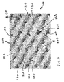
Figure 2 is an exemplary schematic representation of a heat transfer interface structure according to some embodiments. -
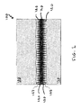
Figure 3 is an exemplary schematic representation of the heat transfer interface structure offigure 2 after compression. -
Figure 4 an exemplary schematic representation of a heat transfer interface structure located between two dies before compression operation. - Conventional thermal interface materials (TIMs) are often composites of thermally conductive particles dispersed in a thermally insulating organic matrix (e.g., adhesive or grease). The thermal conductivity of such composites is limited by the relatively low concentration of particles, as often needed to assure proper viscosity, and by the thermal resistance of particle-particle contacts. Additionally, air-filled voids, which have poor thermal conductivity, can accumulate in the organic matrix, thereby decreasing the overall thermal conductivity of the TIM. Soft metals, such as Indium, or other soft materials, such as graphite, are also sometimes used as thermal interface materials. Although the thermal conductivity of these materials is higher than the composite materials, they have limited ability to comply with non-planar or irregular surfaces. Some of these soft materials are susceptible to corrosion, and, can have low melting points. All of these limitations can restrict reliability, applicability and assembly options.
- An approach for addressing the above drawbacks has been described in
US20090315173 the content of which is herein incorporated by reference in its entirety.US20090315173 discloses various embodiments for a heat transfer structure comprising deformable raised features with a variety of shapes and configurations which may be used according to the specific requirements of each particular use. -
Figure 1 shows a simplified example of aknown interface structure 100. Although the drawing shown infigure 1 is similar to an embodiment as disclosed in the above-referenced document,figure 1 is only provided for illustration purposes and a better understanding of the present disclosure and is not be construed to necessarily include all the features, limitations and/or variants of embodiments of the referencedUS20090315173 . - The
interface structure 100 offigure 1 is intended for use as a heat transfer interface structure between components 130 and 132 havingrespective interface surfaces interface surfaces structure 100 comprises a substrate 110 having raisedfeatures 120. The raisedfeatures 120 are designed to physically contact bothsurfaces surfaces surfaces features 120 may be metallic and deformable and configured to be compressed in at least one dimension as compared to a pre-deformed shape. Compression in the at least one dimension can occur by bending or buckling of the shape of the raised features, or by other modes of changing the shape of the raised features. The direction of compression may be in the direction of arrow A1 or A2 or both. - The raised
features 120 may be located, and in some cases formed directly, on one or more surfaces of a substrate. As shown in the example offigure 1 the raisedfeatures 120 are located on both of the surfaces of a first side and an opposite second side of theplanar substrate 100. In some cases, the substrate itself is a deformable metallic substrate. - The present disclosure departs from a configuration similar to the above-mentioned example of
figure 1 and further provides a structure with additional specific design features and manufacturing techniques as described in further detail below. -
Figure 2 is an exemplary schematic representation of a heat transfer interface structure 200 (herein also referred to as interface structure) according to some embodiments. - In this embodiment, the
interface structure 200 comprises asubstrate 210 and a plurality of raisedfeatures 220. The raisedfeatures 220 are preferably hollow and may be located on both of the surfaces of a first side (e.g. upper side of the structure offigure 2 shown by arrow UP) and an opposite second side (e.g. lower side of the structure offigure 2 which is not visible in the figure), or they may located on only one side thereof. In this regard, the term "raised" is to be understood to refer not only to the features emerging upward from the surface of thesubstrate 210 but also the features emerging downward therefrom. A raisedfeature 220 has abase portion 222 which is the portion proximate to the body of thesubstrate 210 and anend portion 223 opposite to the base portion and being at a certain distance, or at a certain height, from thesubstrate 210. - Preferably the raised features 220 are provided in the form of a two-dimensional array (e.g. length by width relative to the surface of the substrate 210) comprising a continuous plurality of such raised features.
- According to the present disclosure, a raised
feature 220 has anopening 230 at theend portion 223 thereof. Preferably the opening is made by truncating theend portion 223 of the raised feature (i.e. the end portion is cut off transversely with respect to the height of the raised feature). - In
figure 2 , the raised features 220 are shown in the form of truncated domes; however other shapes such as, but not limited to, truncated cones or truncated multi-sided pyramids may also be made. - The proposed shape for the raised features provides certain advantages as compared to the shape of the known raised features which do not have such openings incorporated, because it reduces the stiffness of the features thus presenting less resistance to the compression and flow of metal as the entire structure is compressed. Indeed a raised feature with an opining 230 may bend or buckle with a relatively lower pressure needed to be exerted thereupon (as compared to one without such opening).
- Raised features 220 with
openings 230 may be provided in an array, as shown infigure 2 , comprising a plurality of such features positioned on thesubstrate 210 either randomly or periodically or according to any suitable pattern. Such array may significantly reduce the stress required for the material to conform to surface irregularities and thus provide a lower thermal contact resistance compared to known structures of raised features withoutopenings 230. - Referring now to
figure 3 an exemplary schematic representation of the heat transfer interface structure offigure 2 is provided after such structure has undergone a compression. Infigure 3 , like elements have been given like reference numerals as those offigure 2 . - As can be seen in the compressed structure of
figure 3 , the various elements of the structure have undergone deformation. It is readily observable that the raised features have undergone large-scale compressive deformation including bending and buckling modes resulting in relatively more flattened structures that form a continuous path between the assembled bodies, not shown in the figure (e.g. an electronic component and a heat sink). Such flattened structures may include areas that may come in intimate contact with the compressing surfaces. - For example the raised structure 220-1 of figure may be considered in which the end portion 223-1 is shown to have been compressed, e.g. bent or buckled, toward the base portion 222-1 thereby resulting in a relatively more flattened structure as compared to known structures. The openings of the raised features in the present embodiment therefore allow for obtaining a highly effective thermal and electrical path between the mating components.
- In a highly effective situation, all the compressed raised features may bend or buckle such that all the openings may close as a result of such compression and the collapse of the raised features on the substrate, thereby occupying the open spaces. However, in many practical cases it may occur that not all the raised features actually close the openings upon compression, thereby leaving some areas on the structure still with
openings 230 as shown infigure 3 . The presence of such openings after compression may be remedied by applying grease or adhesive as will be described further below. - A method of manufacturing the interface structure according to some embodiments of the disclosure is described below with reference to
figure 4 . - The interface structure may be manufactured starting from a deformable and preferably flat sheet 410, such as a metal foil. The material of the sheet is chosen so as to posses the heat transfer, electrical and chemical characteristics required for the specific design and application.
- For the sake of clarity with respect to the use of the term heat transfer characteristics, or said in other words, thermal conductivity, as used herein, the following clarification is provided. As it is known, many materials, and even from a pure theoretical standpoint any material, may be considered to be thermally conductive (thus having heat transfer capabilities) as each material has a certain level of thermal conductivity, even if in some cases such level is very low. However, within the context of the present disclosure, a person skilled in the related art would be able to distinguish a material which is considered in the art as thermally conductive from one which is not so considered, such as for example a thermal insulator.
- By way of still further clarification, it is noted that within the context of the present disclosure, any material having a thermal conductivity greater than about 1 W/mK (Watts per Meter Kelvin) may be considered as a thermally conductive material. Conversely, any material having a thermal conductivity of less than about 1 W/mK may be considered as thermally non-conductive. Within the thermal conductivity range described above, a thermal conductivity greater than 100W/mK may be considered as a high thermal conductivity value and one within the range of 1-100W/mK may be considered as an acceptable value.
- Some examples of such materials are given further below.
- The deformable sheet 410 is then placed between two dies 420 and 430 as schematically shown in
figure 4 . The dies 420 and 430 haverespective projections cavities e.g. projections 421 are shown pointing upward in the figure), the projections on the other (opposite) die point in the opposite direction (projections 431 point downward). The dies are then moved toward each other with sufficient force so as to compress and stamp the deformable sheet 410 placed between them. - The
projections cavities - As the dies 420 and 430 are compressed together, the
projections figure 3 . - This manufacturing process not only facilitates the production of desirable interface material geometries, but also it is amenable to high-volume, low-cost fabrication of the interface structure.
- The dies 420 and 430 may be fabricated from a range of materials using various manufacturing techniques known by those skilled in the related art. For example the dies shown in the embodiment of
figure 4 may be fabricated using a 3D printed polymer. - Overall dimensions of the raised features such as height, aspect ratio, metal thickness and feature size or diameter can be designed to suit the specific application which may be determined by, but not limited to, the surface asperities at various length scales (ranging from micro roughness to waviness or larger errors in form) and available assembly pressure. The resulting geometries of the raised features may therefore depend on the geometries of the dies and initial thickness of the deformable sheet, which may vary according to the specific requirements of each design and application.
- Some materials suitable for the interface structure may include a range of malleable and conducting pure metals or alloys. One example is tin due to its low yield strength and reasonably high thermal and electrical conductivity. Depending on the application, assembly pressures or chemical considerations, stiffer, higher conductivity or chemically alternative metals or alloys may be desirable.
- According to one example, applying pressure above 0.5 MPa, provides a structured tin interface material which may demonstrate relatively high effective thermal conductivity and low thermal resistance than a graphite pad. Additionally, due to the large deformation range of this material, it may exhibit greater compliance over a range of pressures. Finally, due to the metallic nature of the tin interface material, it exhibits significantly lower electrical resistance. The aggregated effect of these factors results in significant performance improvements of the present embodiment using tin material for the interface structure material over some commercially available graphite pads.
- After or before the process for forming the interface structure, the material of the interface structure may initially comprise one or more layers of additional material (in the form of a sandwich).
- A further possibility is the use of overlaid material coatings to significantly alter the electrical, thermal and/or chemical response or performance of the interface material. Such coating may be primarily metallic, including but not limited to Gold (Au), Silver (Ag), Copper (Cu), Platinum (Pt), Palladium (Pa), Chrome (Cr), Zinc (Zn) Tin (Sn), Nickel (Ni) or Rhodium (Rh). The coating materials may be pure metals, metal oxides, or alloys containing a mixture of metallic materials, such as Gold Palladium. Preferably a soft metal may be coated with a conductive material (e.g. gold) that is resistant to oxidation and that lowers the electrical contact resistance between mating surfaces. For example, the effect of sputter coating an additional layer of gold on the above embodiment using tin material may offer significant decrease in the electrical resistance over an un-coated interface material. The addition of an alloying over-layer may serve to seal the surface from subsequent oxidation, allowing a longer service lifetime. In order to provide higher levels of compliance to the material of the interface structure, materials with higher levels of ductility may be used such as indium, tin, gallium or lead thereby increasing its capabilities in filling the gaps during compression and allowing it to form a tighter seal when bonded or compressed between layers in its application.
- In this manner, the thermal and electrical properties of the overall TIM are enhanced.
- In some embodiments, it may be desirable to limit the electrical conductivity while maintaining the thermal contact resistance. In such cases electrically insulative coatings such as polymers may be employed to obtain the desired result. Polymer materials are typically good electrical insulators and can be applied in thin, continuous coatings that are compliant. The dielectric coating could be applied either before or after stamping. Applying the coating before stamping is preferred as it may be easier and less expensive to achieve while a variety of coating techniques may be used. However, if it is desired to insure that all surfaces are insulated, the dielectric layer may preferably be applied after the stamping operation to insure that the exposed surface edges generated during compression and punching are coated. One example of an effective approach is to coat the punched film using the polymer Parylene. This polymer dielectric may be deposited from the gas phase insuring conformal coating of uniform thickness over all exposed surfaces. In order to perform the coating process, use may be made of commercially available coating equipment.
- Such coatings may comprise just one additional layer, or several layers in a sandwich-type arrangement. The interfaces between the layers may be discrete and well-defined, or they may consist of inter-metallic layers with have a gradual change in the composition and morphology of the material.
- The coatings may be applied by a number of methods including, but not limited to: in-situ chemical oxidation, by sputter coating using a DC current, by magneto-resistance, by electroplating or electroless plating in a plating bath, or by vapor deposition using metal organic pre-cursors, physical vapors or plasma enhanced methods.
- The compressible solid interface structure may also be used in combination with an interpenetrating continuous phase of grease or adhesive to further improve the thermal, electrical or mechanical properties of the material upon compression. During compression, the raised features allow the flow of a fluid so as to fill gaps which may be formed during such compressions. For example, once compressed and the adhesive cured, the external clamping or assembly pressure may be removed and the thermal and electrical transport capabilities of the interface material would be maintained by the bonding effect of the adhesive. As mentioned previously after the compression it may occur that not all the raised features actually close the respective opening, thereby leaving some areas on the structure with openings. This array of opening permits grease, or adhesive, to flow evenly between the upper and lower interfaces thereby eliminating trapped air and forming an interface with improved thermal performance and, in the case of the adhesive, improved mechanical bond strength.
- Furthermore, the array of openings may also permit the grease or adhesive to flow between upper and lower surfaces of the interface structure forming a uniform thickness of material without significantly increasing the applied stress required for assembly.
- Those skilled in the related art would appreciate that without the openings, air, grease or adhesive, or a combination of these materials could become trapped into pockets. These trapped pockets would increase thermal resistance and increase the required assembly pressure.
- The proposed solution therefore offers improved thermal and electrical performance over conventional interface materials. Additionally, the manufacturing technique described herein is a low-cost alternative to conventional interface techniques. The addition of alternative metallic coatings to the interface material further improves its electrical properties making it a desirable solution for thermal and electrical interface applications.
- The various embodiments of the present disclosure may be combined as long as such combination is compatible and/or complimentary.
- Further it is to be noted that the list of structures corresponding to the claimed means is not exhaustive and that one skilled in the art understands that equivalent structures can be substituted for the recited structure without departing from the scope of the disclosure.
- It is also to be noted that the order of the steps of the method of the invention as described and recited in the corresponding claims is not limited to the order as presented and described and may vary without departing from the scope of the disclosure.
- It should be appreciated by those skilled in the art that any block diagrams herein represent conceptual views of illustrative circuitry embodying the principles of the disclosure.
Claims (16)
- A thermally conductive heat transfer interface structure comprising a substrate having a first surface and a second surface and a plurality of raised features formed on at least one of the first surface and the second surface of the substrate, the raised features being deformable under a compressive force, wherein some of the raised features have an opening at a respective end portion thereof.
- The heat transfer interface structure of claim 1, wherein the structure has the form of a deformable sheet.
- The heat transfer interface structure of claim 1 or claim 2, wherein the opening is at a truncated end portion of the raised feature.
- The heat transfer interface structure of any one of the previous claims, wherein the raised feature is configured to bend or buckle under compression.
- The heat transfer interface structure of any one of the previous claims, wherein a plurality of raised features has the form of an array.
- The heat transfer interface structure of any one of the previous claims, wherein a raised feature is configured to adopt a compressed shape under the compressive force such that the resulting compressed shape is capable of conducting a higher amount of heat than a shape of the raised feature before compression.
- The heat transfer interface structure of claim 1, wherein a raised feature having an opening at an end portion thereof is capable of allowing a flow of a liquid material during compression.
- The heat transfer interface structure of claim 7, wherein the liquid material is grease or adhesive.
- The heat transfer interface structure of any one of the previous claims, wherein the heat transfer interface structure is of a material including a malleable and conductive metals or alloys.
- The heat transfer interface structure of any claim 9, wherein the heat transfer interface structure is made of tin.
- The heat transfer interface structure of any one of the previous claims, wherein the heat transfer interface structure further comprises coating disposed over the heat transfer interface structure, said coating being configured to alter electrical, thermal or chemical characteristics of the heat transfer interface structure.
- The heat transfer interface structure of claim 11, wherein the coating of heat transfer interface structure is configured to provide compliance to the heat transfer interface structure.
- The heat transfer interface structure of claim 11, wherein the coating of heat transfer interface structure is an electrical insulator.
- An apparatus comprising an electric component capable of generating heat, a heat dissipater component and a heat transfer interface structure according to any one of claims 1 to 13, said heat transfer interface structure being located between the electric component and the dissipater component.
- A method, comprising:- placing a deformable sheet of thermally conductive material between two dies each comprising at least one of a projection and a cavity on a respective surface, wherein a projection has a matching shape and dimensions with a cavity;- moving a die toward the other such that a projection nests within a corresponding opposite cavity and such that a compressive force is applied to the deformable sheet located between the projection and the cavity to produce an opening in the deformable sheet.
- The method of claim 14, further comprises applying an interpenetrating liquid during compression, such liquid being capable of flowing between the dies and though the heat transfer interface structure to eliminate air.
Priority Applications (7)
| Application Number | Priority Date | Filing Date | Title |
|---|---|---|---|
| EP13306340.4A EP2854170B1 (en) | 2013-09-27 | 2013-09-27 | A structure for a heat transfer interface and method of manufacturing the same |
| PCT/EP2014/069253 WO2015043947A1 (en) | 2013-09-27 | 2014-09-10 | A structure for a heat transfer interface and method of manufacturing the same |
| EP14814991.7A EP3050096A2 (en) | 2013-09-27 | 2014-09-25 | A structure for a heat transfer interface and method of manufacturing the same |
| PCT/IB2014/002115 WO2015044773A2 (en) | 2013-09-27 | 2014-09-25 | A structure for a heat transfer interface and method of manufacturing the same |
| CN201480052344.5A CN105874591B (en) | 2013-09-27 | 2014-09-25 | Heat transfer interface structure and method of making the same |
| JP2016517441A JP6255089B2 (en) | 2013-09-27 | 2014-09-25 | Structure for heat transfer interface and method of manufacturing the same |
| US14/917,595 US11032942B2 (en) | 2013-09-27 | 2014-09-25 | Structure for a heat transfer interface and method of manufacturing the same |
Applications Claiming Priority (1)
| Application Number | Priority Date | Filing Date | Title |
|---|---|---|---|
| EP13306340.4A EP2854170B1 (en) | 2013-09-27 | 2013-09-27 | A structure for a heat transfer interface and method of manufacturing the same |
Publications (2)
| Publication Number | Publication Date |
|---|---|
| EP2854170A1 true EP2854170A1 (en) | 2015-04-01 |
| EP2854170B1 EP2854170B1 (en) | 2022-01-26 |
Family
ID=49484243
Family Applications (2)
| Application Number | Title | Priority Date | Filing Date |
|---|---|---|---|
| EP13306340.4A Active EP2854170B1 (en) | 2013-09-27 | 2013-09-27 | A structure for a heat transfer interface and method of manufacturing the same |
| EP14814991.7A Withdrawn EP3050096A2 (en) | 2013-09-27 | 2014-09-25 | A structure for a heat transfer interface and method of manufacturing the same |
Family Applications After (1)
| Application Number | Title | Priority Date | Filing Date |
|---|---|---|---|
| EP14814991.7A Withdrawn EP3050096A2 (en) | 2013-09-27 | 2014-09-25 | A structure for a heat transfer interface and method of manufacturing the same |
Country Status (5)
| Country | Link |
|---|---|
| US (1) | US11032942B2 (en) |
| EP (2) | EP2854170B1 (en) |
| JP (1) | JP6255089B2 (en) |
| CN (1) | CN105874591B (en) |
| WO (2) | WO2015043947A1 (en) |
Families Citing this family (5)
| Publication number | Priority date | Publication date | Assignee | Title |
|---|---|---|---|---|
| JP7028788B2 (en) | 2016-03-30 | 2022-03-02 | パーカー・ハニフィン・コーポレーション | Thermal interface material |
| US10777483B1 (en) | 2020-02-28 | 2020-09-15 | Arieca Inc. | Method, apparatus, and assembly for thermally connecting layers |
| JP6849137B1 (en) * | 2020-07-06 | 2021-03-24 | 富士電機株式会社 | Semiconductor device |
| CN115808748A (en) * | 2021-09-14 | 2023-03-17 | 戴尔产品有限公司 | System and method for thermoelectrically cooling optical ports |
| US12700119B2 (en) | 2023-07-27 | 2026-08-04 | Arieca Inc. | Methods and systems for generating a bond line parameter of a circuit assembly, and methods of manufacture of a circuit assembly |
Citations (6)
| Publication number | Priority date | Publication date | Assignee | Title |
|---|---|---|---|---|
| US6374490B1 (en) * | 1998-08-12 | 2002-04-23 | Nakamura Seisakusho Kabushikigaisha | Method of forming a hollow pole projecting on a plate and a method of manufacturing a heat sink using said method |
| WO2002100145A1 (en) * | 2001-06-07 | 2002-12-12 | International Business Machines Corporation | Thermal enhanced extended surface tape for integrated circuit heat dissipation |
| EP1901350A1 (en) * | 2005-07-07 | 2008-03-19 | Kabushiki Kaisha Toyota Jidoshokki | Heat dissipation device and power module |
| US20080290504A1 (en) * | 2007-05-22 | 2008-11-27 | Centipede Systems, Inc. | Compliant thermal contactor |
| US20090315173A1 (en) | 2008-06-20 | 2009-12-24 | Lucent Technologies Inc. | Heat-transfer structure |
| US20120080799A1 (en) * | 2010-09-30 | 2012-04-05 | Infineon Technologies Ag | Semiconductor Module Comprising an Insert and Method for Producing a Semiconductor Module Comprising an Insert |
Family Cites Families (44)
| Publication number | Priority date | Publication date | Assignee | Title |
|---|---|---|---|---|
| US3881799A (en) * | 1972-09-11 | 1975-05-06 | George H Elliott | Resilient multi-micro point metallic junction |
| US5917707A (en) | 1993-11-16 | 1999-06-29 | Formfactor, Inc. | Flexible contact structure with an electrically conductive shell |
| JPS63100759A (en) | 1986-10-17 | 1988-05-02 | Hitachi Ltd | Cooling device for ic chip |
| JPS6476742A (en) | 1987-09-18 | 1989-03-22 | Hitachi Ltd | Heat conductive sheet |
| US5172473A (en) * | 1990-05-07 | 1992-12-22 | International Business Machines Corporation | Method of making cone electrical contact |
| US5542176A (en) | 1992-09-21 | 1996-08-06 | Hideaki Serizawa | Radiation plate and method of producing the same |
| JPH07161881A (en) * | 1993-12-06 | 1995-06-23 | Nippon Telegr & Teleph Corp <Ntt> | Heat conductor for semiconductor element and mounting structure of semiconductor element |
| US6365500B1 (en) | 1994-05-06 | 2002-04-02 | Industrial Technology Research Institute | Composite bump bonding |
| JPH0888300A (en) | 1994-09-19 | 1996-04-02 | Hitachi Ltd | Thermal interface |
| EP0811245A4 (en) | 1995-09-27 | 1998-11-18 | Texas Instruments Inc | MICROELECTRONIC ASSEMBLIES INCLUDING CONDUCTIVE FILMS FOLLOWING THE Z-AXIS |
| US6011694A (en) | 1996-08-01 | 2000-01-04 | Fuji Machinery Mfg. & Electronics Co., Ltd. | Ball grid array semiconductor package with solder ball openings in an insulative base |
| US5786635A (en) | 1996-12-16 | 1998-07-28 | International Business Machines Corporation | Electronic package with compressible heatsink structure |
| US6111314A (en) * | 1998-08-26 | 2000-08-29 | International Business Machines Corporation | Thermal cap with embedded particles |
| JP2000317542A (en) * | 1999-05-12 | 2000-11-21 | Nakamura Seisakusho Kk | Method of forming hollow shaft on plate material |
| AU1348901A (en) | 1999-10-28 | 2001-05-08 | P1 Diamond, Inc. | Improved diamond thermal management components |
| KR100324333B1 (en) | 2000-01-04 | 2002-02-16 | 박종섭 | Stacked package and fabricating method thereof |
| JP4415503B2 (en) | 2000-05-12 | 2010-02-17 | 株式会社デンソー | Semiconductor device |
| JP3280954B2 (en) | 2000-06-02 | 2002-05-13 | 株式会社東芝 | Circuit module and electronic equipment mounted with circuit module |
| JP2002151550A (en) | 2000-11-15 | 2002-05-24 | Nec Corp | Semiconductor device, manufacturing method thereof, coil spring cutting jig and coil spring supply jig used for manufacturing |
| JP2002198473A (en) | 2000-12-26 | 2002-07-12 | Sekisui Chem Co Ltd | Thermal conductive material |
| JP2003017542A (en) | 2001-06-28 | 2003-01-17 | Hitachi Kokusai Electric Inc | Semiconductor manufacturing equipment |
| JP2003031576A (en) | 2001-07-17 | 2003-01-31 | Nec Corp | Semiconductor device and method of manufacturing the same |
| JP3818102B2 (en) * | 2001-08-31 | 2006-09-06 | 住友電気工業株式会社 | Heat dissipation substrate, method for manufacturing the same, and semiconductor device |
| US6638638B2 (en) * | 2001-09-18 | 2003-10-28 | Samsung Electronics Co., Ltd. | Hollow solder structure having improved reliability and method of manufacturing same |
| US20030205363A1 (en) | 2001-11-09 | 2003-11-06 | International Business Machines Corporation | Enhanced air cooling of electronic devices using fluid phase change heat transfer |
| US6758263B2 (en) | 2001-12-13 | 2004-07-06 | Advanced Energy Technology Inc. | Heat dissipating component using high conducting inserts |
| JP2004172489A (en) * | 2002-11-21 | 2004-06-17 | Nec Semiconductors Kyushu Ltd | Semiconductor device and method of manufacturing the same |
| US7005751B2 (en) | 2003-04-10 | 2006-02-28 | Formfactor, Inc. | Layered microelectronic contact and method for fabricating same |
| US7294919B2 (en) | 2003-11-26 | 2007-11-13 | Avago Technologies General Ip (Singapore) Pte. Ltd. | Device having a complaint element pressed between substrates |
| JP4046703B2 (en) | 2004-03-04 | 2008-02-13 | 三菱電機株式会社 | heatsink |
| JP2005322878A (en) | 2004-04-09 | 2005-11-17 | Dainippon Printing Co Ltd | Printed circuit board assembly panel, printed circuit board mounting unit sheet, rigid-flexible circuit board, and manufacturing method thereof |
| JP2006024720A (en) | 2004-07-07 | 2006-01-26 | Nitto Denko Corp | Thermal conductive sheet and semiconductor device using the same |
| JP2006134989A (en) | 2004-11-04 | 2006-05-25 | Mitsubishi Electric Corp | Heat sink, heating element, heat dissipation structure and heat exchanger |
| WO2006076604A2 (en) * | 2005-01-14 | 2006-07-20 | Cabot Corporation | Processes for planarizing substrates and encapsulating printable electronic features |
| CN100458344C (en) | 2005-12-13 | 2009-02-04 | 金龙精密铜管集团股份有限公司 | Copper condensing heat-exchanging pipe for flooded electric refrigerator set |
| US8058101B2 (en) | 2005-12-23 | 2011-11-15 | Tessera, Inc. | Microelectronic packages and methods therefor |
| JP2007294554A (en) | 2006-04-24 | 2007-11-08 | Sumitomo Electric Ind Ltd | Convex structure member |
| KR20090004836A (en) * | 2006-04-24 | 2009-01-12 | 스미토모덴키고교가부시키가이샤 | Heat transfer members, convex structural members, electronic devices, and electrical appliances |
| JP4744360B2 (en) * | 2006-05-22 | 2011-08-10 | 富士通株式会社 | Semiconductor device |
| US7614270B2 (en) * | 2008-02-14 | 2009-11-10 | Ford Global Technologies, Llc | Method and apparatus for superplastic forming |
| CN101981227B (en) * | 2008-03-26 | 2013-08-21 | 默克专利有限公司 | Method for manufacturing semiconductor device |
| US20090242086A1 (en) * | 2008-03-31 | 2009-10-01 | Honda Motor Co., Ltd. | Microstructural optimization of automotive structures |
| JP5280102B2 (en) * | 2008-05-26 | 2013-09-04 | ルネサスエレクトロニクス株式会社 | Manufacturing method of semiconductor device |
| US8289712B2 (en) * | 2010-06-21 | 2012-10-16 | International Business Machines Corporation | Flux-free detachable thermal interface between an integrated circuit device and a heat sink |
-
2013
- 2013-09-27 EP EP13306340.4A patent/EP2854170B1/en active Active
-
2014
- 2014-09-10 WO PCT/EP2014/069253 patent/WO2015043947A1/en not_active Ceased
- 2014-09-25 WO PCT/IB2014/002115 patent/WO2015044773A2/en not_active Ceased
- 2014-09-25 CN CN201480052344.5A patent/CN105874591B/en active Active
- 2014-09-25 EP EP14814991.7A patent/EP3050096A2/en not_active Withdrawn
- 2014-09-25 JP JP2016517441A patent/JP6255089B2/en active Active
- 2014-09-25 US US14/917,595 patent/US11032942B2/en active Active
Patent Citations (6)
| Publication number | Priority date | Publication date | Assignee | Title |
|---|---|---|---|---|
| US6374490B1 (en) * | 1998-08-12 | 2002-04-23 | Nakamura Seisakusho Kabushikigaisha | Method of forming a hollow pole projecting on a plate and a method of manufacturing a heat sink using said method |
| WO2002100145A1 (en) * | 2001-06-07 | 2002-12-12 | International Business Machines Corporation | Thermal enhanced extended surface tape for integrated circuit heat dissipation |
| EP1901350A1 (en) * | 2005-07-07 | 2008-03-19 | Kabushiki Kaisha Toyota Jidoshokki | Heat dissipation device and power module |
| US20080290504A1 (en) * | 2007-05-22 | 2008-11-27 | Centipede Systems, Inc. | Compliant thermal contactor |
| US20090315173A1 (en) | 2008-06-20 | 2009-12-24 | Lucent Technologies Inc. | Heat-transfer structure |
| US20120080799A1 (en) * | 2010-09-30 | 2012-04-05 | Infineon Technologies Ag | Semiconductor Module Comprising an Insert and Method for Producing a Semiconductor Module Comprising an Insert |
Also Published As
| Publication number | Publication date |
|---|---|
| US11032942B2 (en) | 2021-06-08 |
| CN105874591A (en) | 2016-08-17 |
| WO2015044773A2 (en) | 2015-04-02 |
| EP3050096A2 (en) | 2016-08-03 |
| WO2015044773A3 (en) | 2015-08-06 |
| JP6255089B2 (en) | 2017-12-27 |
| JP2016533634A (en) | 2016-10-27 |
| WO2015043947A1 (en) | 2015-04-02 |
| CN105874591B (en) | 2019-03-29 |
| US20160219751A1 (en) | 2016-07-28 |
| EP2854170B1 (en) | 2022-01-26 |
Similar Documents
| Publication | Publication Date | Title |
|---|---|---|
| JP7825187B2 (en) | solid electrolytic capacitor | |
| US11032942B2 (en) | Structure for a heat transfer interface and method of manufacturing the same | |
| KR101323877B1 (en) | A heat-transfer structure | |
| JP7203323B2 (en) | Solid electrolytic capacitor and manufacturing method thereof | |
| KR101054251B1 (en) | Conductive Contact Terminals for Board Surface Mount | |
| KR20190044535A (en) | Method for manufacturing solid electrolytic capacitor and solid electrolytic capacitor | |
| JPWO2011111112A1 (en) | Heat dissipating structure, electronic device and manufacturing method thereof | |
| TW201222757A (en) | Connector assembly and method of manufacture | |
| CN102725804B (en) | For the surface mount resistor with terminal and the manufacture method thereof of high energy dissipation | |
| JP2011090865A (en) | Conductive film and manufacturing method therefor, and semiconductor device and manufacturing method therefor | |
| JP2011090865A5 (en) | ||
| US20110095433A1 (en) | Conductive film, method of manufacturing the same, semiconductor device and method of manufacturing the same | |
| CN110391044B (en) | A flexible wire based on composite liquid metal | |
| JPWO2003079495A1 (en) | Flexible good conductive layer and anisotropic conductive sheet using the same | |
| JP5065993B2 (en) | Crimp terminal for aluminum wire | |
| CN107809012B (en) | It is suitable for the centreless elastic electric contact terminal of low clearance | |
| CN104517866A (en) | Method for producing a power semiconductor device with a soldered joint | |
| CN107667419B (en) | Method for manufacturing a circuit carrier | |
| CN103928418A (en) | Bonding wire and method for producing a bond connection | |
| CN100477387C (en) | Anisotropic conductive sheet and method for producing same | |
| US10388627B1 (en) | Micro-bonding structure and method of forming the same | |
| JPWO2003079494A1 (en) | Anisotropic conductive sheet and manufacturing method thereof | |
| JP7559996B2 (en) | Solid electrolytic capacitors and capacitor arrays | |
| JP2003017158A (en) | Pressure contact type sheet connector and manufacturing method thereof | |
| KR101468128B1 (en) | Copper or Copper Alloy foil and Assembly of the same |
Legal Events
| Date | Code | Title | Description |
|---|---|---|---|
| PUAI | Public reference made under article 153(3) epc to a published international application that has entered the european phase |
Free format text: ORIGINAL CODE: 0009012 |
|
| 17P | Request for examination filed |
Effective date: 20130927 |
|
| AK | Designated contracting states |
Kind code of ref document: A1 Designated state(s): AL AT BE BG CH CY CZ DE DK EE ES FI FR GB GR HR HU IE IS IT LI LT LU LV MC MK MT NL NO PL PT RO RS SE SI SK SM TR |
|
| AX | Request for extension of the european patent |
Extension state: BA ME |
|
| R17P | Request for examination filed (corrected) |
Effective date: 20151001 |
|
| RBV | Designated contracting states (corrected) |
Designated state(s): AL AT BE BG CH CY CZ DE DK EE ES FI FR GB GR HR HU IE IS IT LI LT LU LV MC MK MT NL NO PL PT RO RS SE SI SK SM TR |
|
| 17Q | First examination report despatched |
Effective date: 20161017 |
|
| STAA | Information on the status of an ep patent application or granted ep patent |
Free format text: STATUS: EXAMINATION IS IN PROGRESS |
|
| RAP1 | Party data changed (applicant data changed or rights of an application transferred) |
Owner name: ALCATEL LUCENT |
|
| REG | Reference to a national code |
Ref country code: DE Ref legal event code: R079 Ref document number: 602013080775 Country of ref document: DE Free format text: PREVIOUS MAIN CLASS: H01L0023373000 Ipc: H01L0021480000 |
|
| RIC1 | Information provided on ipc code assigned before grant |
Ipc: F28F 13/00 20060101ALI20210406BHEP Ipc: B21D 13/02 20060101ALI20210406BHEP Ipc: B21D 53/04 20060101ALI20210406BHEP Ipc: B21D 33/00 20060101ALI20210406BHEP Ipc: H01L 23/42 20060101ALI20210406BHEP Ipc: H01L 23/433 20060101ALI20210406BHEP Ipc: H01L 23/373 20060101ALI20210406BHEP Ipc: H01L 21/48 20060101AFI20210406BHEP |
|
| GRAP | Despatch of communication of intention to grant a patent |
Free format text: ORIGINAL CODE: EPIDOSNIGR1 |
|
| STAA | Information on the status of an ep patent application or granted ep patent |
Free format text: STATUS: GRANT OF PATENT IS INTENDED |
|
| INTG | Intention to grant announced |
Effective date: 20210517 |
|
| GRAJ | Information related to disapproval of communication of intention to grant by the applicant or resumption of examination proceedings by the epo deleted |
Free format text: ORIGINAL CODE: EPIDOSDIGR1 |
|
| STAA | Information on the status of an ep patent application or granted ep patent |
Free format text: STATUS: EXAMINATION IS IN PROGRESS |
|
| INTC | Intention to grant announced (deleted) | ||
| GRAP | Despatch of communication of intention to grant a patent |
Free format text: ORIGINAL CODE: EPIDOSNIGR1 |
|
| STAA | Information on the status of an ep patent application or granted ep patent |
Free format text: STATUS: GRANT OF PATENT IS INTENDED |
|
| INTG | Intention to grant announced |
Effective date: 20211110 |
|
| GRAS | Grant fee paid |
Free format text: ORIGINAL CODE: EPIDOSNIGR3 |
|
| GRAA | (expected) grant |
Free format text: ORIGINAL CODE: 0009210 |
|
| STAA | Information on the status of an ep patent application or granted ep patent |
Free format text: STATUS: THE PATENT HAS BEEN GRANTED |
|
| AK | Designated contracting states |
Kind code of ref document: B1 Designated state(s): AL AT BE BG CH CY CZ DE DK EE ES FI FR GB GR HR HU IE IS IT LI LT LU LV MC MK MT NL NO PL PT RO RS SE SI SK SM TR |
|
| REG | Reference to a national code |
Ref country code: GB Ref legal event code: FG4D |
|
| REG | Reference to a national code |
Ref country code: CH Ref legal event code: EP |
|
| REG | Reference to a national code |
Ref country code: AT Ref legal event code: REF Ref document number: 1465933 Country of ref document: AT Kind code of ref document: T Effective date: 20220215 |
|
| REG | Reference to a national code |
Ref country code: IE Ref legal event code: FG4D |
|
| REG | Reference to a national code |
Ref country code: DE Ref legal event code: R096 Ref document number: 602013080775 Country of ref document: DE |
|
| REG | Reference to a national code |
Ref country code: LT Ref legal event code: MG9D |
|
| REG | Reference to a national code |
Ref country code: NL Ref legal event code: MP Effective date: 20220126 |
|
| REG | Reference to a national code |
Ref country code: AT Ref legal event code: MK05 Ref document number: 1465933 Country of ref document: AT Kind code of ref document: T Effective date: 20220126 |
|
| PG25 | Lapsed in a contracting state [announced via postgrant information from national office to epo] |
Ref country code: NL Free format text: LAPSE BECAUSE OF FAILURE TO SUBMIT A TRANSLATION OF THE DESCRIPTION OR TO PAY THE FEE WITHIN THE PRESCRIBED TIME-LIMIT Effective date: 20220126 |
|
| PG25 | Lapsed in a contracting state [announced via postgrant information from national office to epo] |
Ref country code: SE Free format text: LAPSE BECAUSE OF FAILURE TO SUBMIT A TRANSLATION OF THE DESCRIPTION OR TO PAY THE FEE WITHIN THE PRESCRIBED TIME-LIMIT Effective date: 20220126 Ref country code: RS Free format text: LAPSE BECAUSE OF FAILURE TO SUBMIT A TRANSLATION OF THE DESCRIPTION OR TO PAY THE FEE WITHIN THE PRESCRIBED TIME-LIMIT Effective date: 20220126 Ref country code: PT Free format text: LAPSE BECAUSE OF FAILURE TO SUBMIT A TRANSLATION OF THE DESCRIPTION OR TO PAY THE FEE WITHIN THE PRESCRIBED TIME-LIMIT Effective date: 20220526 Ref country code: NO Free format text: LAPSE BECAUSE OF FAILURE TO SUBMIT A TRANSLATION OF THE DESCRIPTION OR TO PAY THE FEE WITHIN THE PRESCRIBED TIME-LIMIT Effective date: 20220426 Ref country code: LT Free format text: LAPSE BECAUSE OF FAILURE TO SUBMIT A TRANSLATION OF THE DESCRIPTION OR TO PAY THE FEE WITHIN THE PRESCRIBED TIME-LIMIT Effective date: 20220126 Ref country code: HR Free format text: LAPSE BECAUSE OF FAILURE TO SUBMIT A TRANSLATION OF THE DESCRIPTION OR TO PAY THE FEE WITHIN THE PRESCRIBED TIME-LIMIT Effective date: 20220126 Ref country code: ES Free format text: LAPSE BECAUSE OF FAILURE TO SUBMIT A TRANSLATION OF THE DESCRIPTION OR TO PAY THE FEE WITHIN THE PRESCRIBED TIME-LIMIT Effective date: 20220126 Ref country code: BG Free format text: LAPSE BECAUSE OF FAILURE TO SUBMIT A TRANSLATION OF THE DESCRIPTION OR TO PAY THE FEE WITHIN THE PRESCRIBED TIME-LIMIT Effective date: 20220426 |
|
| PG25 | Lapsed in a contracting state [announced via postgrant information from national office to epo] |
Ref country code: PL Free format text: LAPSE BECAUSE OF FAILURE TO SUBMIT A TRANSLATION OF THE DESCRIPTION OR TO PAY THE FEE WITHIN THE PRESCRIBED TIME-LIMIT Effective date: 20220126 Ref country code: LV Free format text: LAPSE BECAUSE OF FAILURE TO SUBMIT A TRANSLATION OF THE DESCRIPTION OR TO PAY THE FEE WITHIN THE PRESCRIBED TIME-LIMIT Effective date: 20220126 Ref country code: GR Free format text: LAPSE BECAUSE OF FAILURE TO SUBMIT A TRANSLATION OF THE DESCRIPTION OR TO PAY THE FEE WITHIN THE PRESCRIBED TIME-LIMIT Effective date: 20220427 Ref country code: FI Free format text: LAPSE BECAUSE OF FAILURE TO SUBMIT A TRANSLATION OF THE DESCRIPTION OR TO PAY THE FEE WITHIN THE PRESCRIBED TIME-LIMIT Effective date: 20220126 Ref country code: AT Free format text: LAPSE BECAUSE OF FAILURE TO SUBMIT A TRANSLATION OF THE DESCRIPTION OR TO PAY THE FEE WITHIN THE PRESCRIBED TIME-LIMIT Effective date: 20220126 |
|
| PG25 | Lapsed in a contracting state [announced via postgrant information from national office to epo] |
Ref country code: IS Free format text: LAPSE BECAUSE OF FAILURE TO SUBMIT A TRANSLATION OF THE DESCRIPTION OR TO PAY THE FEE WITHIN THE PRESCRIBED TIME-LIMIT Effective date: 20220526 |
|
| REG | Reference to a national code |
Ref country code: DE Ref legal event code: R097 Ref document number: 602013080775 Country of ref document: DE |
|
| PG25 | Lapsed in a contracting state [announced via postgrant information from national office to epo] |
Ref country code: SM Free format text: LAPSE BECAUSE OF FAILURE TO SUBMIT A TRANSLATION OF THE DESCRIPTION OR TO PAY THE FEE WITHIN THE PRESCRIBED TIME-LIMIT Effective date: 20220126 Ref country code: SK Free format text: LAPSE BECAUSE OF FAILURE TO SUBMIT A TRANSLATION OF THE DESCRIPTION OR TO PAY THE FEE WITHIN THE PRESCRIBED TIME-LIMIT Effective date: 20220126 Ref country code: RO Free format text: LAPSE BECAUSE OF FAILURE TO SUBMIT A TRANSLATION OF THE DESCRIPTION OR TO PAY THE FEE WITHIN THE PRESCRIBED TIME-LIMIT Effective date: 20220126 Ref country code: EE Free format text: LAPSE BECAUSE OF FAILURE TO SUBMIT A TRANSLATION OF THE DESCRIPTION OR TO PAY THE FEE WITHIN THE PRESCRIBED TIME-LIMIT Effective date: 20220126 Ref country code: DK Free format text: LAPSE BECAUSE OF FAILURE TO SUBMIT A TRANSLATION OF THE DESCRIPTION OR TO PAY THE FEE WITHIN THE PRESCRIBED TIME-LIMIT Effective date: 20220126 Ref country code: CZ Free format text: LAPSE BECAUSE OF FAILURE TO SUBMIT A TRANSLATION OF THE DESCRIPTION OR TO PAY THE FEE WITHIN THE PRESCRIBED TIME-LIMIT Effective date: 20220126 |
|
| PG25 | Lapsed in a contracting state [announced via postgrant information from national office to epo] |
Ref country code: AL Free format text: LAPSE BECAUSE OF FAILURE TO SUBMIT A TRANSLATION OF THE DESCRIPTION OR TO PAY THE FEE WITHIN THE PRESCRIBED TIME-LIMIT Effective date: 20220126 |
|
| PLBE | No opposition filed within time limit |
Free format text: ORIGINAL CODE: 0009261 |
|
| STAA | Information on the status of an ep patent application or granted ep patent |
Free format text: STATUS: NO OPPOSITION FILED WITHIN TIME LIMIT |
|
| 26N | No opposition filed |
Effective date: 20221027 |
|
| PG25 | Lapsed in a contracting state [announced via postgrant information from national office to epo] |
Ref country code: SI Free format text: LAPSE BECAUSE OF FAILURE TO SUBMIT A TRANSLATION OF THE DESCRIPTION OR TO PAY THE FEE WITHIN THE PRESCRIBED TIME-LIMIT Effective date: 20220126 |
|
| PG25 | Lapsed in a contracting state [announced via postgrant information from national office to epo] |
Ref country code: MC Free format text: LAPSE BECAUSE OF FAILURE TO SUBMIT A TRANSLATION OF THE DESCRIPTION OR TO PAY THE FEE WITHIN THE PRESCRIBED TIME-LIMIT Effective date: 20220126 |
|
| REG | Reference to a national code |
Ref country code: CH Ref legal event code: PL |
|
| GBPC | Gb: european patent ceased through non-payment of renewal fee |
Effective date: 20220927 |
|
| REG | Reference to a national code |
Ref country code: BE Ref legal event code: MM Effective date: 20220930 |
|
| PG25 | Lapsed in a contracting state [announced via postgrant information from national office to epo] |
Ref country code: LU Free format text: LAPSE BECAUSE OF NON-PAYMENT OF DUE FEES Effective date: 20220927 |
|
| PG25 | Lapsed in a contracting state [announced via postgrant information from national office to epo] |
Ref country code: LI Free format text: LAPSE BECAUSE OF NON-PAYMENT OF DUE FEES Effective date: 20220930 Ref country code: IT Free format text: LAPSE BECAUSE OF FAILURE TO SUBMIT A TRANSLATION OF THE DESCRIPTION OR TO PAY THE FEE WITHIN THE PRESCRIBED TIME-LIMIT Effective date: 20220126 Ref country code: IE Free format text: LAPSE BECAUSE OF NON-PAYMENT OF DUE FEES Effective date: 20220927 Ref country code: CH Free format text: LAPSE BECAUSE OF NON-PAYMENT OF DUE FEES Effective date: 20220930 |
|
| PG25 | Lapsed in a contracting state [announced via postgrant information from national office to epo] |
Ref country code: BE Free format text: LAPSE BECAUSE OF NON-PAYMENT OF DUE FEES Effective date: 20220930 |
|
| PG25 | Lapsed in a contracting state [announced via postgrant information from national office to epo] |
Ref country code: GB Free format text: LAPSE BECAUSE OF NON-PAYMENT OF DUE FEES Effective date: 20220927 |
|
| PG25 | Lapsed in a contracting state [announced via postgrant information from national office to epo] |
Ref country code: HU Free format text: LAPSE BECAUSE OF FAILURE TO SUBMIT A TRANSLATION OF THE DESCRIPTION OR TO PAY THE FEE WITHIN THE PRESCRIBED TIME-LIMIT; INVALID AB INITIO Effective date: 20130927 |
|
| PG25 | Lapsed in a contracting state [announced via postgrant information from national office to epo] |
Ref country code: CY Free format text: LAPSE BECAUSE OF FAILURE TO SUBMIT A TRANSLATION OF THE DESCRIPTION OR TO PAY THE FEE WITHIN THE PRESCRIBED TIME-LIMIT Effective date: 20220126 |
|
| PG25 | Lapsed in a contracting state [announced via postgrant information from national office to epo] |
Ref country code: MK Free format text: LAPSE BECAUSE OF FAILURE TO SUBMIT A TRANSLATION OF THE DESCRIPTION OR TO PAY THE FEE WITHIN THE PRESCRIBED TIME-LIMIT Effective date: 20220126 |
|
| PG25 | Lapsed in a contracting state [announced via postgrant information from national office to epo] |
Ref country code: MT Free format text: LAPSE BECAUSE OF FAILURE TO SUBMIT A TRANSLATION OF THE DESCRIPTION OR TO PAY THE FEE WITHIN THE PRESCRIBED TIME-LIMIT Effective date: 20220126 |
|
| PGFP | Annual fee paid to national office [announced via postgrant information from national office to epo] |
Ref country code: DE Payment date: 20250805 Year of fee payment: 13 |
|
| PGFP | Annual fee paid to national office [announced via postgrant information from national office to epo] |
Ref country code: FR Payment date: 20250808 Year of fee payment: 13 |
|
| REG | Reference to a national code |
Ref country code: DE Ref legal event code: R079 Ref document number: 602013080775 Country of ref document: DE Free format text: PREVIOUS MAIN CLASS: H01L0021480000 Ipc: H10W0076010000 |
|
| PG25 | Lapsed in a contracting state [announced via postgrant information from national office to epo] |
Ref country code: TR Free format text: LAPSE BECAUSE OF FAILURE TO SUBMIT A TRANSLATION OF THE DESCRIPTION OR TO PAY THE FEE WITHIN THE PRESCRIBED TIME-LIMIT Effective date: 20220126 |