EP2852054A1 - High speed amplifier - Google Patents
High speed amplifier Download PDFInfo
- Publication number
- EP2852054A1 EP2852054A1 EP20140181177 EP14181177A EP2852054A1 EP 2852054 A1 EP2852054 A1 EP 2852054A1 EP 20140181177 EP20140181177 EP 20140181177 EP 14181177 A EP14181177 A EP 14181177A EP 2852054 A1 EP2852054 A1 EP 2852054A1
- Authority
- EP
- European Patent Office
- Prior art keywords
- circuit
- transistors
- biasing
- terminal
- transistor
- Prior art date
- Legal status (The legal status is an assumption and is not a legal conclusion. Google has not performed a legal analysis and makes no representation as to the accuracy of the status listed.)
- Granted
Links
- 239000000758 substrate Substances 0.000 claims abstract description 39
- 230000003071 parasitic effect Effects 0.000 claims abstract description 5
- 238000012544 monitoring process Methods 0.000 claims description 3
- 238000010586 diagram Methods 0.000 description 4
- 238000009792 diffusion process Methods 0.000 description 2
- 239000002184 metal Substances 0.000 description 2
- 229910044991 metal oxide Inorganic materials 0.000 description 2
- 150000004706 metal oxides Chemical class 0.000 description 2
- 238000000034 method Methods 0.000 description 2
- 229910052710 silicon Inorganic materials 0.000 description 2
- 239000010703 silicon Substances 0.000 description 2
- 230000006978 adaptation Effects 0.000 description 1
- 238000003491 array Methods 0.000 description 1
- 238000004519 manufacturing process Methods 0.000 description 1
- 239000000463 material Substances 0.000 description 1
- 238000012986 modification Methods 0.000 description 1
- 230000004048 modification Effects 0.000 description 1
- 238000006467 substitution reaction Methods 0.000 description 1
Images


Classifications
-
- H—ELECTRICITY
- H03—ELECTRONIC CIRCUITRY
- H03F—AMPLIFIERS
- H03F3/00—Amplifiers with only discharge tubes or only semiconductor devices as amplifying elements
- H03F3/189—High frequency amplifiers, e.g. radio frequency amplifiers
- H03F3/19—High frequency amplifiers, e.g. radio frequency amplifiers with semiconductor devices only
- H03F3/193—High frequency amplifiers, e.g. radio frequency amplifiers with semiconductor devices only with field-effect devices
-
- H—ELECTRICITY
- H03—ELECTRONIC CIRCUITRY
- H03F—AMPLIFIERS
- H03F1/00—Details of amplifiers with only discharge tubes, only semiconductor devices or only unspecified devices as amplifying elements
- H03F1/02—Modifications of amplifiers to raise the efficiency, e.g. gliding Class A stages, use of an auxiliary oscillation
- H03F1/0205—Modifications of amplifiers to raise the efficiency, e.g. gliding Class A stages, use of an auxiliary oscillation in transistor amplifiers
- H03F1/0261—Modifications of amplifiers to raise the efficiency, e.g. gliding Class A stages, use of an auxiliary oscillation in transistor amplifiers with control of the polarisation voltage or current, e.g. gliding Class A
- H03F1/0266—Modifications of amplifiers to raise the efficiency, e.g. gliding Class A stages, use of an auxiliary oscillation in transistor amplifiers with control of the polarisation voltage or current, e.g. gliding Class A by using a signal derived from the input signal
-
- H—ELECTRICITY
- H03—ELECTRONIC CIRCUITRY
- H03F—AMPLIFIERS
- H03F3/00—Amplifiers with only discharge tubes or only semiconductor devices as amplifying elements
- H03F3/189—High frequency amplifiers, e.g. radio frequency amplifiers
- H03F3/19—High frequency amplifiers, e.g. radio frequency amplifiers with semiconductor devices only
- H03F3/193—High frequency amplifiers, e.g. radio frequency amplifiers with semiconductor devices only with field-effect devices
- H03F3/1935—High frequency amplifiers, e.g. radio frequency amplifiers with semiconductor devices only with field-effect devices with junction-FET devices
-
- H—ELECTRICITY
- H03—ELECTRONIC CIRCUITRY
- H03F—AMPLIFIERS
- H03F3/00—Amplifiers with only discharge tubes or only semiconductor devices as amplifying elements
- H03F3/189—High frequency amplifiers, e.g. radio frequency amplifiers
- H03F3/19—High frequency amplifiers, e.g. radio frequency amplifiers with semiconductor devices only
- H03F3/195—High frequency amplifiers, e.g. radio frequency amplifiers with semiconductor devices only in integrated circuits
-
- H—ELECTRICITY
- H03—ELECTRONIC CIRCUITRY
- H03F—AMPLIFIERS
- H03F2200/00—Indexing scheme relating to amplifiers
- H03F2200/18—Indexing scheme relating to amplifiers the bias of the gate of a FET being controlled by a control signal
-
- H—ELECTRICITY
- H03—ELECTRONIC CIRCUITRY
- H03K—PULSE TECHNIQUE
- H03K2217/00—Indexing scheme related to electronic switching or gating, i.e. not by contact-making or -breaking covered by H03K17/00
- H03K2217/0018—Special modifications or use of the back gate voltage of a FET
Definitions
- the non-dominant pole may need to be pushed out to high frequencies.
- a low non-dominant pole frequency can lead to bad phase margin (underdamped behavior) and low bandwidth.
- the amplifier may be designed with increased current in the output stage of the amplifier to increase the gm of the output stage. This, however, may lead to increasing power consumption. Additionally, as gm/C may be inherently limited by manufacturing process, increasing current may not be sufficient to increase the non-dominant pole of the output stage.
- a circuit comprising: one or more transistors connected directly to an output; and a biasing network connected to at least one of a substrate, a well, and a back-gate of at least one of the transistors, wherein the biasing network biases the at least one of the substrate, the well, and the back-gate to a virtual floating bias, such that the virtual floating bias shifts in voltage level based upon an AC input signal of the circuit.
- the one or more transistors may be connected in series with each other to form an amplifier.
- the biasing network may comprise one of a switch and a resistor.
- the biasing network may comprise a resistor that is connected to the at least one of the transistors at a first terminal and connected to a DC voltage at a second terminal.
- the biasing network may comprise a switch that is connected to the at least one of the transistors at a first terminal, a DC voltage at a second terminal, and a floating node at a third terminal, wherein the switch adjusts biasing by switching between the second terminal and the third terminal.
- the switch may adjust biasing by switching to the second terminal during a reset phase of the circuit, and switching to the third terminal during an operational phase of the circuit.
- a controller may control the switch to adjusts biasing based upon monitoring of voltage of the at least one of the substrate, the well, and the back-gate of the at least one of the transistors.
- a circuit comprising: one or more transistors connected directly to an output; and a biasing network connected to at least one of a substrate, a well, and a back-gate of at least one of the transistors, wherein the biasing network biases the at least one of the substrate, the well, and the back-gate to a virtual floating bias, such that the virtual floating bias reduces parasitic capacitance of the output.
- the one or more transistors may be connected in series with each other to form an amplifier.
- the biasing network may comprise one of a switch and a resistor.
- the biasing network may comprise a resistor that is connected to the at least one of the transistors at a first terminal and connected to a DC voltage at a second terminal.
- the biasing network may comprise a switch that is connected to the at least one of the transistors at a first terminal, a DC voltage at a second terminal, and a floating node at a third terminal, wherein the switch adjusts biasing by switching between the second terminal and the third terminal.
- the switch may adjust biasing by switching to the second terminal during a reset phase of the circuit, and switching to the third terminal during an operational phase of the circuit.
- a controller control the switch to adjusts biasing based upon monitoring of voltage of the at least one of the substrate, the well, and the back-gate of the at least one of the transistors.
- a circuit comprising: one or more transistors connected directly to an output; and a biasing network connected to at least one of a substrate, a well, and a back-gate of at least one of the transistors, wherein the biasing network biases the at least one of the substrate, the well, and the back-gate to a virtual floating bias, such that the virtual floating bias increases a frequency of a non-dominant frequency response pole of an AC input signal of the circuit.
- the one or more transistors may be connected in series with each other to form an amplifier.
- the biasing network may comprise one of a switch and a resistor.
- the biasing network may comprise a resistor that is connected to the at least one of the transistors at a first terminal and connected to a DC voltage at a second terminal.
- the biasing network may comprise a switch that is connected to the at least one of the transistors at a first terminal, a DC voltage at a second terminal, and a floating node at a third terminal, wherein the switch adjusts biasing by switching between the second terminal and the third terminal.
- the switch may adjust biasing by switching to the second terminal during a reset phase of the circuit, and switching to the third terminal during an operational phase of the circuit.
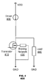
- a circuit 100 may include a transistor 110, and a biasing network 120.
- the transistor 110 may be output on an output node to drive a load 140.
- the biasing network 120 may be connected to the transistor 110 to bias at least one of a substrate and a back-gate of the transistor 110 to a virtual floating bias, such that at least one of a substrate, a well, and a back-gate of the transistor 110 shifts in voltage level when the output node outputs an AC signal.
- circuit 100 may be an amplifier circuit.
- Transistor 110 may be a PMOS (P-type Metal Oxide Silicon) transistor.
- Transistor 110 may have a gate connected to an input AC signal to be amplified.
- Driver 130 may be a current driver connected in series with the transistor 110 between supplies VDD and GND, to generate the output node to drive the load 140.
- transistor 110 may be a current driving transistor configured to bias a current through the amplifier circuit 100.
- the driver 130 may receive the input signal to be amplified.
- transistor 110 may be connected to VDD on its source node, to the output node on its drain node, and the back-gate (or NWELL) is in series with the biasing network 120 to the supply VDD.
- the transistor 110 may have one of its back-gate, substrate, and well connected to the biasing network 120, such that the biasing network 120 controls the biasing on one of the back-gate, substrate, and well of the transistor 110 to be a virtual floating bias.
- the virtual floating bias may be such that when the output of the transistor 110 outputs lower frequency range signals, one of its back-gate, substrate, and well of the transistor 110 appears to be floating, i.e. able to shift voltage level according to the signal at the input and the output.
- FIG. 2 illustrates an idealized cross-sectional diagram of the transistor 110.
- the transistor 110 may be a PMOS with a gate 202 with a gate oxide layer 204, a P-doped source region 206, a P-doped drain region 208, a N-doped well region 210, a P type substrate 212.
- the transistor 110 may have one of its N-doped well region (back-gate) 210, P type substrate 212, connected to biasing network 120.
- biasing network 120 may be connected to DC biasing voltages, to prevent forward biasing substrate junctions of the transistor 410.
- FIG. 3 illustrates a biasing network 120.
- the biasing network 120 may include one of a resistor 122, and a switch 124.
- the virtual float bias may be done by connecting one of back-gate, substrate, and well of the transistor 110 to a biasing voltage (for example, VDD or GND), through a very large resistor, for example having resistance of 200 kilo-ohms to 1 mega-ohms, that effectively one of its back-gate, substrate, and well of the transistor 110 to act as a floating node or an open circuit in the low frequency range of the circuit 100.
- a biasing voltage for example, VDD or GND
- one of back-gate, substrate, and well of the transistor 110 may be connected to a switch 124, to be switched between two states, where one of back-gate, substrate, and well of the transistor 110 may be connected to a bias voltage (for example, VDD or GND) in a reset (off) phase (when the circuit 100 is not operational or resetting), and floated completely in the operational phase (when the circuit 100 is operating to output signal).
- the back-gate, the substrate, or the well may be set to a DC bias voltage to effective reset the transistor 110 to prevent drifting of the transistor voltage levels.
- the switch 124 may be controlled by a controller (not shown) to periodically enter reset phases to prevent drifting of the transistor voltage levels. The controller may monitor the average DC voltage levels of transistors, and if determined that the voltage levels of the back-gate, the substrate, or the well are drifting from desired levels, the controller may control the switch 124 to enter the reset phase.
- the parasitic capacitances of the transistor 110 may appear in series with the capacitances of the well, the substrate, the back-gate, and hence there effective capacitance value on the output node is greatly reduced, particularly in the lower frequency range.
- a circuit 400 may include a transistor 410, and a biasing network 420.
- the transistor 410 may be output on an output node to drive a load 440.
- the biasing network 420 may be connected to the transistor 410 to bias at least one of a substrate, a deep N well, and a back-gate of the transistor 410 (P-type) to a virtual floating bias, such that at least one of a substrate, a well, and a back-gate of the transistor 410 shifts in voltage level when the output node outputs an AC signal.
- circuit 400 may be an amplifier circuit.
- Transistor 410 may be a NMOS (N-type Metal Oxide Silicon) transistor.
- Transistor 410 may have a gate connected to an input AC signal to be amplified.
- Driver 430 may be a current driver connected in series with the transistor 410 between supplies VDD and GND, to generate the output node to drive the load 440.
- transistor 410 may be a current driving transistor configured to bias a current through the amplifier circuit 400.
- the driver 430 may receive the input signal to be amplified.
- transistor 410 may be connected to GND on its source node, to the output node on its drain node, and in series with the biasing network 420 to the supply GND.
- the transistor 410 may have one of its back-gate, substrate, and well connected to the biasing network 420, such that the biasing network 420 controls the biasing on one of the back-gate, substrate, and well of the transistor 410 to be a virtual floating bias.
- the virtual floating bias may be such that when the output of the transistor 410 outputs lower frequency range signals, one of its back-gate, substrate, and well of the transistor 410 appears to be floating, i.e. able to shift voltage level according to the signal at the input and the output.
- FIG. 5 illustrates an idealized cross-sectional diagram of the transistor 410.
- the transistor 410 may be a NMOS with a gate 502 with a gate oxide layer 504, a N-doped source region 506, a N-doped drain region 508, a P-doped well region 510 (backgate), a deep N-doped well region 518, a P type substrate 512.
- the transistor 410 may have one of its P-doped well region 510, deep N-doped well region 518, P type substrate 512, and back-gate 514 connected to biasing network 420.
- Various taps such as diffusion or metal taps, may be implemented in the above portions of transistor 410 to connect to the biasing network 420.
- the biasing network 420 may be connected to DC biasing voltages, to prevent forward biasing substrate junctions of the transistor 410.
- FIG. 6 illustrates a circuit 600 according an embodiment.
- Circuit 600 may include a plurality of transistors 610.1-610.5 and a plurality of biasing networks 620.1-620.4, configured in similar manners as in circuits 100 and circuits 400 of FIGS. 1 and 4 .
- Circuit 600 may be configured as a differential pair amplifier driving differential outputs connected to a load 640.
- Circuit 600 may be configured as a differential pair amplifier where each differential branch may be configured as a cascode amplifier.
- Transistors 610.1-610.4 may be connected to the differential output nodes on their respective drain nodes, and transistor 610.5 may be a biasing transistor. According to an embodiment, only the transistors 610.1-610.4 which are connected directly on their drain or source nodes to the output nodes, need to be connected to a respective biasing network 620.1-620.4. Thus, transistor 610.5 may not need to have its own biasing network, and may be directly connected to a DC bias (for example GND) on its substrate, well, and/or back-gate. Transistors 610.1-610.4 may share a single biasing network, or have separate biasing networks, with same or separate biasing nodes implementing separate or connected virtual floating biases. The biasing networks 620.1-620.4 may be implemented on the same circuit unit or chip as the transistors 610.1-610.4 or on separate circuit units or chips.
- Transistors 610.1 and 610.2 may be PMOS transistors as similar to transistor 110 in FIGS. 1 and 2
- transistors 610.3 and 610.4 may be NMOS transistors as similar to transistor 410 in FIGS. 4 and 5 .
- FIG. 7 illustrates a circuit 700 according an embodiment.
- Circuit 700 may include a plurality of transistors 710.1-710.10 and a plurality of biasing networks 720.1-720.8, configured in similar manners as in circuits 100 and circuits 400 of FIGS. 1 and 4 .
- Circuit 700 may be configured as a two-staged differential pair amplifier driving differential outputs connected to a load 740.
- Circuit 700 may be configured as a two-staged differential pair amplifier where each differential branch may be configured as a cascode amplifier.
- Transistors 710.1-710.8 may be connected to the differential output nodes on their respective drain nodes, and transistors 710.9 and 710.10 may be biasing transistors. According to an embodiment, only the transistors 710.1-710.8 which are connected directly on their drain or source nodes to the output nodes, need to be connected to a respective biasing network 720.1-720.8. Thus, transistors 710.9 and 710.10 may not need to have its own biasing network, and may be directly connected to a DC bias (for example GND) on its substrate, well, and/or back-gate. Transistors 710.1-710.8 may share a single biasing network, or have separate biasing networks, with same or separate biasing nodes implementing separate or connected virtual floating biases. The biasing networks 720.1-720.8 may be implemented on the same circuit unit or chip as the transistors 710.1-710.8 or on separate circuit units or chips.
- Transistors 710.1-710.2 and 710.5-710.6 may be PMOS transistors as similar to transistor 110 in FIGS. 1 and 2
- transistors 710.3-710.4 and 710.7-710.8 may be NMOS transistors as similar to transistor 410 in FIGS. 4 and 5 .
Abstract
Description
- In an amplifier, there may be a non-dominant frequency pole whose frequency value is proportional to gm/C, where gm is the transconductance of the output stage and C is the total capacitance at the output node (for example, C may include the capacitance of the load at the output node, the capacitance of the output node itself, and parasitic capacitances).
- For high speed applications, the non-dominant pole may need to be pushed out to high frequencies. A low non-dominant pole frequency can lead to bad phase margin (underdamped behavior) and low bandwidth. To increase the frequency of the non-dominant pole, the amplifier may be designed with increased current in the output stage of the amplifier to increase the gm of the output stage. This, however, may lead to increasing power consumption. Additionally, as gm/C may be inherently limited by manufacturing process, increasing current may not be sufficient to increase the non-dominant pole of the output stage.
- Accordingly, there is a need for an amplifier with increased or improved non-dominant pole frequencies with improved bandwidth and settling time, without increasing the current of the output stage.
- According to a first aspect of the present disclosure there is provided a circuit, comprising: one or more transistors connected directly to an output; and a biasing network connected to at least one of a substrate, a well, and a back-gate of at least one of the transistors, wherein the biasing network biases the at least one of the substrate, the well, and the back-gate to a virtual floating bias, such that the virtual floating bias shifts in voltage level based upon an AC input signal of the circuit.
- The one or more transistors may be connected in series with each other to form an amplifier.
- The biasing network may comprise one of a switch and a resistor.
- The biasing network may comprise a resistor that is connected to the at least one of the transistors at a first terminal and connected to a DC voltage at a second terminal.
- The biasing network may comprise a switch that is connected to the at least one of the transistors at a first terminal, a DC voltage at a second terminal, and a floating node at a third terminal, wherein the switch adjusts biasing by switching between the second terminal and the third terminal.
- The switch may adjust biasing by switching to the second terminal during a reset phase of the circuit, and switching to the third terminal during an operational phase of the circuit.
- A controller may control the switch to adjusts biasing based upon monitoring of voltage of the at least one of the substrate, the well, and the back-gate of the at least one of the transistors.
- According to a second aspect of the present disclosure there is provided a circuit, comprising: one or more transistors connected directly to an output; and a biasing network connected to at least one of a substrate, a well, and a back-gate of at least one of the transistors, wherein the biasing network biases the at least one of the substrate, the well, and the back-gate to a virtual floating bias, such that the virtual floating bias reduces parasitic capacitance of the output.
- The one or more transistors may be connected in series with each other to form an amplifier.
- The biasing network may comprise one of a switch and a resistor.
- The biasing network may comprise a resistor that is connected to the at least one of the transistors at a first terminal and connected to a DC voltage at a second terminal.
- The biasing network may comprise a switch that is connected to the at least one of the transistors at a first terminal, a DC voltage at a second terminal, and a floating node at a third terminal, wherein the switch adjusts biasing by switching between the second terminal and the third terminal.
- The switch may adjust biasing by switching to the second terminal during a reset phase of the circuit, and switching to the third terminal during an operational phase of the circuit.
- A controller control the switch to adjusts biasing based upon monitoring of voltage of the at least one of the substrate, the well, and the back-gate of the at least one of the transistors.
- According to a third aspect of the present disclosure there is provided a circuit, comprising: one or more transistors connected directly to an output; and a biasing network connected to at least one of a substrate, a well, and a back-gate of at least one of the transistors, wherein the biasing network biases the at least one of the substrate, the well, and the back-gate to a virtual floating bias, such that the virtual floating bias increases a frequency of a non-dominant frequency response pole of an AC input signal of the circuit.
- The one or more transistors may be connected in series with each other to form an amplifier.
- The biasing network may comprise one of a switch and a resistor.
- The biasing network may comprise a resistor that is connected to the at least one of the transistors at a first terminal and connected to a DC voltage at a second terminal.
- The biasing network may comprise a switch that is connected to the at least one of the transistors at a first terminal, a DC voltage at a second terminal, and a floating node at a third terminal, wherein the switch adjusts biasing by switching between the second terminal and the third terminal.
- The switch may adjust biasing by switching to the second terminal during a reset phase of the circuit, and switching to the third terminal during an operational phase of the circuit.
-
-
FIG. 1 illustrates a circuit according to an embodiment of the present disclosure. -
FIG. 2 illustrates a cross-sectional diagram of a transistor in a circuit according to an embodiment of the present disclosure. -
FIG. 3 illustrates a biasing network according to an embodiment of the present disclosure. -
FIG. 4 illustrates a circuit according to an embodiment of the present disclosure. -
FIG. 5 illustrates a cross-sectional diagram of a transistor in a circuit according to an embodiment of the present disclosure. -
FIG. 6 illustrates a circuit according to an embodiment of the present disclosure. -
FIG. 7 illustrates a circuit according to an embodiment of the present disclosure. - According to an embodiment illustrated in
FIG. 1 , a circuit 100 may include atransistor 110, and abiasing network 120. Thetransistor 110 may be output on an output node to drive aload 140. Thebiasing network 120 may be connected to thetransistor 110 to bias at least one of a substrate and a back-gate of thetransistor 110 to a virtual floating bias, such that at least one of a substrate, a well, and a back-gate of thetransistor 110 shifts in voltage level when the output node outputs an AC signal. - In
FIG. 1 , circuit 100 may be an amplifier circuit.Transistor 110 may be a PMOS (P-type Metal Oxide Silicon) transistor.Transistor 110 may have a gate connected to an input AC signal to be amplified.Driver 130 may be a current driver connected in series with thetransistor 110 between supplies VDD and GND, to generate the output node to drive theload 140. - Alternatively,
transistor 110 may be a current driving transistor configured to bias a current through the amplifier circuit 100. In such a case, thedriver 130 may receive the input signal to be amplified. - In the above configurations,
transistor 110 may be connected to VDD on its source node, to the output node on its drain node, and the back-gate (or NWELL) is in series with thebiasing network 120 to the supply VDD. Thetransistor 110 may have one of its back-gate, substrate, and well connected to thebiasing network 120, such that thebiasing network 120 controls the biasing on one of the back-gate, substrate, and well of thetransistor 110 to be a virtual floating bias. The virtual floating bias may be such that when the output of thetransistor 110 outputs lower frequency range signals, one of its back-gate, substrate, and well of thetransistor 110 appears to be floating, i.e. able to shift voltage level according to the signal at the input and the output. -
FIG. 2 illustrates an idealized cross-sectional diagram of thetransistor 110. - The
transistor 110 may be a PMOS with agate 202 with agate oxide layer 204, a P-dopedsource region 206, a P-dopeddrain region 208, a N-dopedwell region 210, aP type substrate 212. - According to an embodiment implemented in circuit 100, the
transistor 110 may have one of its N-doped well region (back-gate) 210,P type substrate 212, connected tobiasing network 120. Various taps, such as diffusion or metal taps, may be implemented in the above portions oftransistor 110 to connect to thebiasing network 120. Additionally, thebiasing network 120 may be connected to DC biasing voltages, to prevent forward biasing substrate junctions of thetransistor 410. -
FIG. 3 illustrates abiasing network 120. - The
biasing network 120 may include one of aresistor 122, and aswitch 124. - The virtual float bias may be done by connecting one of back-gate, substrate, and well of the
transistor 110 to a biasing voltage (for example, VDD or GND), through a very large resistor, for example having resistance of 200 kilo-ohms to 1 mega-ohms, that effectively one of its back-gate, substrate, and well of thetransistor 110 to act as a floating node or an open circuit in the low frequency range of the circuit 100. - Alternatively, one of back-gate, substrate, and well of the
transistor 110 may be connected to aswitch 124, to be switched between two states, where one of back-gate, substrate, and well of thetransistor 110 may be connected to a bias voltage (for example, VDD or GND) in a reset (off) phase (when the circuit 100 is not operational or resetting), and floated completely in the operational phase (when the circuit 100 is operating to output signal). In the reset phase, the back-gate, the substrate, or the well may be set to a DC bias voltage to effective reset thetransistor 110 to prevent drifting of the transistor voltage levels. Additionally theswitch 124 may be controlled by a controller (not shown) to periodically enter reset phases to prevent drifting of the transistor voltage levels. The controller may monitor the average DC voltage levels of transistors, and if determined that the voltage levels of the back-gate, the substrate, or the well are drifting from desired levels, the controller may control theswitch 124 to enter the reset phase. - By virtual floating one of back-gate, substrate, and well of the
transistor 110, the parasitic capacitances of thetransistor 110 may appear in series with the capacitances of the well, the substrate, the back-gate, and hence there effective capacitance value on the output node is greatly reduced, particularly in the lower frequency range. - According to an embodiment illustrated in
FIG. 4 , a circuit 400 may include atransistor 410, and abiasing network 420. Thetransistor 410 may be output on an output node to drive aload 440. Thebiasing network 420 may be connected to thetransistor 410 to bias at least one of a substrate, a deep N well, and a back-gate of the transistor 410 (P-type) to a virtual floating bias, such that at least one of a substrate, a well, and a back-gate of thetransistor 410 shifts in voltage level when the output node outputs an AC signal. - In
FIG. 4 , circuit 400 may be an amplifier circuit.Transistor 410 may be a NMOS (N-type Metal Oxide Silicon) transistor.Transistor 410 may have a gate connected to an input AC signal to be amplified.Driver 430 may be a current driver connected in series with thetransistor 410 between supplies VDD and GND, to generate the output node to drive theload 440. - Alternatively,
transistor 410 may be a current driving transistor configured to bias a current through the amplifier circuit 400. In such a case, thedriver 430 may receive the input signal to be amplified. - In the above configurations,
transistor 410 may be connected to GND on its source node, to the output node on its drain node, and in series with thebiasing network 420 to the supply GND. Thetransistor 410 may have one of its back-gate, substrate, and well connected to thebiasing network 420, such that thebiasing network 420 controls the biasing on one of the back-gate, substrate, and well of thetransistor 410 to be a virtual floating bias. The virtual floating bias may be such that when the output of thetransistor 410 outputs lower frequency range signals, one of its back-gate, substrate, and well of thetransistor 410 appears to be floating, i.e. able to shift voltage level according to the signal at the input and the output. -
FIG. 5 illustrates an idealized cross-sectional diagram of thetransistor 410. - The
transistor 410 may be a NMOS with agate 502 with agate oxide layer 504, a N-dopedsource region 506, a N-dopeddrain region 508, a P-doped well region 510 (backgate), a deep N-dopedwell region 518, aP type substrate 512. - According to an embodiment implemented in circuit 400, the
transistor 410 may have one of its P-dopedwell region 510, deep N-dopedwell region 518,P type substrate 512, and back-gate 514 connected to biasingnetwork 420. Various taps, such as diffusion or metal taps, may be implemented in the above portions oftransistor 410 to connect to thebiasing network 420. Additionally, thebiasing network 420 may be connected to DC biasing voltages, to prevent forward biasing substrate junctions of thetransistor 410. -
FIG. 6 illustrates a circuit 600 according an embodiment. - Circuit 600 may include a plurality of transistors 610.1-610.5 and a plurality of biasing networks 620.1-620.4, configured in similar manners as in circuits 100 and circuits 400 of
FIGS. 1 and4 . Circuit 600 may be configured as a differential pair amplifier driving differential outputs connected to aload 640. Circuit 600 may be configured as a differential pair amplifier where each differential branch may be configured as a cascode amplifier. - Transistors 610.1-610.4 may be connected to the differential output nodes on their respective drain nodes, and transistor 610.5 may be a biasing transistor. According to an embodiment, only the transistors 610.1-610.4 which are connected directly on their drain or source nodes to the output nodes, need to be connected to a respective biasing network 620.1-620.4. Thus, transistor 610.5 may not need to have its own biasing network, and may be directly connected to a DC bias (for example GND) on its substrate, well, and/or back-gate. Transistors 610.1-610.4 may share a single biasing network, or have separate biasing networks, with same or separate biasing nodes implementing separate or connected virtual floating biases. The biasing networks 620.1-620.4 may be implemented on the same circuit unit or chip as the transistors 610.1-610.4 or on separate circuit units or chips.
- Transistors 610.1 and 610.2 may be PMOS transistors as similar to
transistor 110 inFIGS. 1 and2 , and transistors 610.3 and 610.4 may be NMOS transistors as similar totransistor 410 inFIGS. 4 and5 . -
FIG. 7 illustrates a circuit 700 according an embodiment. - Circuit 700 may include a plurality of transistors 710.1-710.10 and a plurality of biasing networks 720.1-720.8, configured in similar manners as in circuits 100 and circuits 400 of
FIGS. 1 and4 . Circuit 700 may be configured as a two-staged differential pair amplifier driving differential outputs connected to aload 740. Circuit 700 may be configured as a two-staged differential pair amplifier where each differential branch may be configured as a cascode amplifier. - Transistors 710.1-710.8 may be connected to the differential output nodes on their respective drain nodes, and transistors 710.9 and 710.10 may be biasing transistors. According to an embodiment, only the transistors 710.1-710.8 which are connected directly on their drain or source nodes to the output nodes, need to be connected to a respective biasing network 720.1-720.8. Thus, transistors 710.9 and 710.10 may not need to have its own biasing network, and may be directly connected to a DC bias (for example GND) on its substrate, well, and/or back-gate. Transistors 710.1-710.8 may share a single biasing network, or have separate biasing networks, with same or separate biasing nodes implementing separate or connected virtual floating biases. The biasing networks 720.1-720.8 may be implemented on the same circuit unit or chip as the transistors 710.1-710.8 or on separate circuit units or chips.
- Transistors 710.1-710.2 and 710.5-710.6 may be PMOS transistors as similar to
transistor 110 inFIGS. 1 and2 , and transistors 710.3-710.4 and 710.7-710.8 may be NMOS transistors as similar totransistor 410 inFIGS. 4 and5 . - It is appreciated that the disclosure is not limited to the described embodiments, and that any number of scenarios and embodiments in which conflicting appointments exist may be resolved.
- Although the disclosure has been described with reference to several exemplary embodiments, it is understood that the words that have been used are words of description and illustration, rather than words of limitation. Changes may be made within the purview of the appended claims, as presently stated and as amended, without departing from the scope and spirit of the disclosure in its aspects. Although the disclosure has been described with reference to particular means, materials and embodiments, the disclosure is not intended to be limited to the particulars disclosed; rather the disclosure extends to all functionally equivalent structures, methods, and uses such as are within the scope of the appended claims.
- Although the present application describes specific embodiments which may be implemented as code segments in computer-readable media, it is to be understood that dedicated hardware implementations, such as application specific integrated circuits, programmable logic arrays and other hardware devices, can be constructed to implement one or more of the embodiments described herein. Applications that may include the various embodiments set forth herein may broadly include a variety of electronic and computer systems. Accordingly, the present application may encompass software, firmware, and hardware implementations, or combinations thereof.
- The present specification describes components and functions that may be implemented in particular embodiments with reference to particular standards and protocols, the disclosure is not limited to such standards and protocols. Such standards are periodically superseded by faster or more efficient equivalents having essentially the same functions. Accordingly, replacement standards and protocols having the same or similar functions are considered equivalents thereof.
- The illustrations of the embodiments described herein are intended to provide a general understanding of the various embodiments. The illustrations are not intended to serve as a complete description of all of the elements and features of apparatus and systems that utilize the structures or methods described herein. Many other embodiments may be apparent to those of skill in the art upon reviewing the disclosure. Other embodiments may be utilized and derived from the disclosure, such that structural and logical substitutions and changes may be made without departing from the scope of the disclosure. Additionally, the illustrations are merely representational and may not be drawn to scale. Certain proportions within the illustrations may be exaggerated, while other proportions may be minimized. Accordingly, the disclosure and the figures are to be regarded as illustrative rather than restrictive.
- One or more embodiments of the disclosure may be referred to herein, individually and/or collectively, by the term "disclosure" merely for convenience and without intending to voluntarily limit the scope of this application to any particular disclosure or inventive concept. Moreover, although specific embodiments have been illustrated and described herein, it should be appreciated that any subsequent arrangement designed to achieve the same or similar purpose may be substituted for the specific embodiments shown. This disclosure is intended to cover any and all subsequent adaptations or variations of various embodiments. Combinations of the above embodiments, and other embodiments not specifically described herein, will be apparent to those of skill in the art upon reviewing the description.
- In addition, in the foregoing Detailed Description, various features may be grouped together or described in a single embodiment for the purpose of streamlining the disclosure. This disclosure is not to be interpreted as reflecting an intention that the claimed embodiments require more features than are expressly recited in each claim. Rather, as the following claims reflect, inventive subject matter may be directed to less than all of the features of any of the disclosed embodiments. Thus, the following claims are incorporated into the Detailed Description, with each claim standing on its own as defining separately claimed subject matter.
- The above disclosed subject matter is to be considered illustrative, and not restrictive, and the appended claims are intended to cover all such modifications, enhancements, and other embodiments which fall within the true spirit and scope of the present disclosure. Thus, to the maximum extent allowed by law, the scope of the present disclosure is to be determined by the broadest permissible interpretation of the following claims and their equivalents, and shall not be restricted or limited by the foregoing detailed description.
Claims (7)
- A circuit, comprising:one or more transistors connected directly to an output; anda biasing network connected to at least one of a substrate, a well, and a back-gate of at least one of the transistors,wherein the biasing network biases the at least one of the substrate, the well, and the back-gate to a virtual floating bias, such that one or more of the following occurs:the virtual floating bias shifts in voltage level based upon an AC input signal of the circuit,the virtual floating bias reduces parasitic capacitance of the output; orthe virtual floating bias increases a frequency of a non-dominant frequency response pole of an AC input signal of the circuit.
- The circuit of claim 1, wherein the one or more transistors are connected in series with each other to form an amplifier.
- The circuit of claim 1, wherein the biasing network comprises one of a switch and a resistor.
- The circuit of claim 1, wherein the biasing network comprises a resistor that is connected to the at least one of the transistors at a first terminal and connected to a DC voltage at a second terminal.
- The circuit of claim 1, wherein the biasing network comprises a switch that is connected to the at least one of the transistors at a first terminal, a DC voltage at a second terminal, and a floating node at a third terminal, wherein the switch adjusts biasing by switching between the second terminal and the third terminal.
- The circuit of claim 5, wherein the switch adjusts biasing by switching to the second terminal during a reset phase of the circuit, and switching to the third terminal during an operational phase of the circuit.
- The circuit of claim 5, wherein a controller controls the switch to adjusts biasing based upon monitoring of voltage of the at least one of the substrate, the well, and the back-gate of the at least one of the transistors.
Applications Claiming Priority (1)
| Application Number | Priority Date | Filing Date | Title |
|---|---|---|---|
| US14/012,165 US9276534B2 (en) | 2013-08-28 | 2013-08-28 | High speed amplifier |
Publications (2)
| Publication Number | Publication Date |
|---|---|
| EP2852054A1 true EP2852054A1 (en) | 2015-03-25 |
| EP2852054B1 EP2852054B1 (en) | 2018-06-13 |
Family
ID=51302949
Family Applications (1)
| Application Number | Title | Priority Date | Filing Date |
|---|---|---|---|
| EP14181177.8A Active EP2852054B1 (en) | 2013-08-28 | 2014-08-15 | High speed amplifier |
Country Status (3)
| Country | Link |
|---|---|
| US (1) | US9276534B2 (en) |
| EP (1) | EP2852054B1 (en) |
| CN (1) | CN104426494B (en) |
Families Citing this family (6)
| Publication number | Priority date | Publication date | Assignee | Title |
|---|---|---|---|---|
| US10886382B2 (en) * | 2017-02-15 | 2021-01-05 | Skyworks Solutions, Inc. | Cascode amplifier optimization |
| US10211825B2 (en) * | 2017-06-07 | 2019-02-19 | Globalfoundries Inc. | Circuits having a switch with back-gate bias |
| US11558019B2 (en) * | 2018-11-15 | 2023-01-17 | Taiwan Semiconductor Manufacturing Co., Ltd. | Method and circuit to isolate body capacitance in semiconductor devices |
| CN111193478A (en) | 2018-11-15 | 2020-05-22 | 台湾积体电路制造股份有限公司 | Amplifying circuit |
| CN112148060B (en) * | 2019-06-26 | 2022-05-17 | 圣邦微电子(北京)股份有限公司 | Input stage substrate voltage control circuit of crossover-distortion-free operational amplifier |
| CN111488722B (en) * | 2020-04-16 | 2022-12-27 | 清华大学 | Design method for full-customized low-leakage digital circuit standard unit |
Citations (6)
| Publication number | Priority date | Publication date | Assignee | Title |
|---|---|---|---|---|
| JPH02301321A (en) * | 1989-05-16 | 1990-12-13 | Sanyo Electric Co Ltd | Integrated circuit |
| US20030076172A1 (en) * | 2001-09-27 | 2003-04-24 | Powerq Technologies, Inc. | Amplifier circuits and methods |
| US6586958B2 (en) * | 2000-02-29 | 2003-07-01 | Seiko Instruments Inc. | Voltage converter having switching element with variable substrate potential |
| US20030141929A1 (en) * | 2002-01-31 | 2003-07-31 | Intel Corporation | Differential amplifier offset adjustment |
| US20080315950A1 (en) * | 2007-06-06 | 2008-12-25 | Samsung Electronics Co., Ltd. | Integrated Circuit Amplifiers Having Switch Circuits Therein that Provide Reduced 1/f Noise |
| US20120139643A1 (en) * | 2010-12-05 | 2012-06-07 | Amalfi Semiconductor, Inc. | Output Stage of a Power Amplifier Having a Switched-Bulk Biasing and Adaptive Biasing |
Family Cites Families (11)
| Publication number | Priority date | Publication date | Assignee | Title |
|---|---|---|---|---|
| US6046641A (en) | 1998-07-22 | 2000-04-04 | Eni Technologies, Inc. | Parallel HV MOSFET high power stable amplifier |
| US6064262A (en) * | 1998-09-25 | 2000-05-16 | Lucent Technologies Inc. | CMOS differential amplifier having offset voltage cancellation and common-mode voltage control |
| US6750711B2 (en) | 2001-04-13 | 2004-06-15 | Eni Technology, Inc. | RF power amplifier stability |
| KR100689743B1 (en) | 2004-10-01 | 2007-03-08 | 삼성전자주식회사 | Electro Static Discharge Protection and Input Impedance Matching Circuit for Low Noise Amplifier And Low Noise Amplifier |
| US7688152B2 (en) | 2006-07-10 | 2010-03-30 | Triquint Semiconductor, Inc | High frequency stabilization network for microwave devices and monolithic integrated circuits |
| KR100732070B1 (en) * | 2007-03-07 | 2007-06-27 | (주)에프씨아이 | Low noise amplifier with variable gain |
| WO2009044441A1 (en) | 2007-10-01 | 2009-04-09 | Fujitsu Limited | Single differential converter and rf receiver |
| US7714652B2 (en) * | 2008-04-07 | 2010-05-11 | Semiconductor Components Industries, Llc | Method for adjusting threshold voltage and circuit therefor |
| US8213142B2 (en) | 2008-10-29 | 2012-07-03 | Qualcomm, Incorporated | Amplifier with improved ESD protection circuitry |
| US8577325B2 (en) | 2010-08-31 | 2013-11-05 | Korea Advanced Institute Of Science And Technology | Low noise amplifier having both ultra-high linearity and low noise characteristic and radio receiver including the same |
| JP5714470B2 (en) | 2011-11-21 | 2015-05-07 | サムソン エレクトロ−メカニックス カンパニーリミテッド. | CMOS integrated circuit and amplifier circuit |
-
2013
- 2013-08-28 US US14/012,165 patent/US9276534B2/en active Active
-
2014
- 2014-08-15 EP EP14181177.8A patent/EP2852054B1/en active Active
- 2014-08-28 CN CN201410431476.0A patent/CN104426494B/en active Active
Patent Citations (6)
| Publication number | Priority date | Publication date | Assignee | Title |
|---|---|---|---|---|
| JPH02301321A (en) * | 1989-05-16 | 1990-12-13 | Sanyo Electric Co Ltd | Integrated circuit |
| US6586958B2 (en) * | 2000-02-29 | 2003-07-01 | Seiko Instruments Inc. | Voltage converter having switching element with variable substrate potential |
| US20030076172A1 (en) * | 2001-09-27 | 2003-04-24 | Powerq Technologies, Inc. | Amplifier circuits and methods |
| US20030141929A1 (en) * | 2002-01-31 | 2003-07-31 | Intel Corporation | Differential amplifier offset adjustment |
| US20080315950A1 (en) * | 2007-06-06 | 2008-12-25 | Samsung Electronics Co., Ltd. | Integrated Circuit Amplifiers Having Switch Circuits Therein that Provide Reduced 1/f Noise |
| US20120139643A1 (en) * | 2010-12-05 | 2012-06-07 | Amalfi Semiconductor, Inc. | Output Stage of a Power Amplifier Having a Switched-Bulk Biasing and Adaptive Biasing |
Non-Patent Citations (2)
| Title |
|---|
| SCHLOGL F ET AL: "1.5 GHz OPAMP in 120nm digital CMOS", SOLID-STATE CIRCUITS CONFERENCE, 2004. ESSCIRC 2004. PROCEEDING OF THE 30TH EUROPEAN, IEEE, PISCATAWAY, NJ, USA, 21 September 2004 (2004-09-21), pages 239 - 242, XP010738531, ISBN: 978-0-7803-8480-4, DOI: 10.1109/ESSCIR.2004.1356662 * |
| SOCHEAT HENG ET AL: "A Low-Power High-PSRR Low-Dropout Regulator With Bulk-Gate Controlled Circuit", IEEE TRANSACTIONS ON CIRCUITS AND SYSTEMS II: EXPRESS BRIEFS, IEEE, US, vol. 57, no. 4, 1 April 2010 (2010-04-01), pages 245 - 249, XP011334182, ISSN: 1549-7747, DOI: 10.1109/TCSII.2010.2043390 * |
Also Published As
| Publication number | Publication date |
|---|---|
| CN104426494B (en) | 2018-01-12 |
| EP2852054B1 (en) | 2018-06-13 |
| US20150061776A1 (en) | 2015-03-05 |
| US9276534B2 (en) | 2016-03-01 |
| CN104426494A (en) | 2015-03-18 |
Similar Documents
| Publication | Publication Date | Title |
|---|---|---|
| EP2852054A1 (en) | High speed amplifier | |
| US8350624B2 (en) | Amplifiers and related biasing methods and devices | |
| US7391825B2 (en) | Comparator circuit having reduced pulse width distortion | |
| CN107947757B (en) | Impedance circuit | |
| US7276961B2 (en) | Constant voltage outputting circuit | |
| KR100691349B1 (en) | Differential circuit, output buffer circuit and semiconductor integrated circuit used for multi-power system | |
| CN107004638B (en) | Semiconductor integrated circuit having a plurality of transistors | |
| CN106230432B (en) | High-speed signal level conversion circuit with low power consumption and ultra wide bandwidth | |
| USRE47432E1 (en) | Output stage circuit | |
| TWI529398B (en) | Analog minimum or maximum voltage selector circuit | |
| JP2008252029A (en) | Semiconductor device | |
| JP3764158B2 (en) | Data output circuit | |
| JP2007534244A (en) | Output stage system | |
| US8836027B2 (en) | Switch circuit using LDMOS element | |
| US20150381160A1 (en) | Robust multiplexer, and method for operating a robust multiplexer | |
| WO2019094451A1 (en) | Differential input stages | |
| CN105843322B (en) | Voltage reference circuit and working method thereof | |
| CN112684841B (en) | Low dropout regulator with high power supply rejection ratio | |
| US9166047B2 (en) | Switch circuit using LDMOS device | |
| US10348288B2 (en) | Differential output circuit | |
| JP2016187123A (en) | Comparator circuit | |
| KR102469122B1 (en) | Dual mode supply circuit and method | |
| JP2017147560A (en) | Level shift circuit | |
| US9276532B2 (en) | High speed amplifier | |
| JPH1168548A (en) | Semiconductor integrated circuit |
Legal Events
| Date | Code | Title | Description |
|---|---|---|---|
| PUAI | Public reference made under article 153(3) epc to a published international application that has entered the european phase |
Free format text: ORIGINAL CODE: 0009012 |
|
| 17P | Request for examination filed |
Effective date: 20140815 |
|
| AK | Designated contracting states |
Kind code of ref document: A1 Designated state(s): AL AT BE BG CH CY CZ DE DK EE ES FI FR GB GR HR HU IE IS IT LI LT LU LV MC MK MT NL NO PL PT RO RS SE SI SK SM TR |
|
| AX | Request for extension of the european patent |
Extension state: BA ME |
|
| R17P | Request for examination filed (corrected) |
Effective date: 20150924 |
|
| RBV | Designated contracting states (corrected) |
Designated state(s): AL AT BE BG CH CY CZ DE DK EE ES FI FR GB GR HR HU IE IS IT LI LT LU LV MC MK MT NL NO PL PT RO RS SE SI SK SM TR |
|
| STAA | Information on the status of an ep patent application or granted ep patent |
Free format text: STATUS: EXAMINATION IS IN PROGRESS |
|
| 17Q | First examination report despatched |
Effective date: 20170816 |
|
| GRAP | Despatch of communication of intention to grant a patent |
Free format text: ORIGINAL CODE: EPIDOSNIGR1 |
|
| STAA | Information on the status of an ep patent application or granted ep patent |
Free format text: STATUS: GRANT OF PATENT IS INTENDED |
|
| INTG | Intention to grant announced |
Effective date: 20180117 |
|
| GRAS | Grant fee paid |
Free format text: ORIGINAL CODE: EPIDOSNIGR3 |
|
| GRAA | (expected) grant |
Free format text: ORIGINAL CODE: 0009210 |
|
| STAA | Information on the status of an ep patent application or granted ep patent |
Free format text: STATUS: THE PATENT HAS BEEN GRANTED |
|
| AK | Designated contracting states |
Kind code of ref document: B1 Designated state(s): AL AT BE BG CH CY CZ DE DK EE ES FI FR GB GR HR HU IE IS IT LI LT LU LV MC MK MT NL NO PL PT RO RS SE SI SK SM TR |
|
| REG | Reference to a national code |
Ref country code: GB Ref legal event code: FG4D |
|
| REG | Reference to a national code |
Ref country code: CH Ref legal event code: EP Ref country code: AT Ref legal event code: REF Ref document number: 1009530 Country of ref document: AT Kind code of ref document: T Effective date: 20180615 |
|
| REG | Reference to a national code |
Ref country code: DE Ref legal event code: R096 Ref document number: 602014026885 Country of ref document: DE |
|
| REG | Reference to a national code |
Ref country code: IE Ref legal event code: FG4D |
|
| REG | Reference to a national code |
Ref country code: NL Ref legal event code: MP Effective date: 20180613 |
|
| REG | Reference to a national code |
Ref country code: LT Ref legal event code: MG4D |
|
| PG25 | Lapsed in a contracting state [announced via postgrant information from national office to epo] |
Ref country code: ES Free format text: LAPSE BECAUSE OF FAILURE TO SUBMIT A TRANSLATION OF THE DESCRIPTION OR TO PAY THE FEE WITHIN THE PRESCRIBED TIME-LIMIT Effective date: 20180613 Ref country code: SE Free format text: LAPSE BECAUSE OF FAILURE TO SUBMIT A TRANSLATION OF THE DESCRIPTION OR TO PAY THE FEE WITHIN THE PRESCRIBED TIME-LIMIT Effective date: 20180613 Ref country code: CY Free format text: LAPSE BECAUSE OF FAILURE TO SUBMIT A TRANSLATION OF THE DESCRIPTION OR TO PAY THE FEE WITHIN THE PRESCRIBED TIME-LIMIT Effective date: 20180613 Ref country code: BG Free format text: LAPSE BECAUSE OF FAILURE TO SUBMIT A TRANSLATION OF THE DESCRIPTION OR TO PAY THE FEE WITHIN THE PRESCRIBED TIME-LIMIT Effective date: 20180913 Ref country code: NO Free format text: LAPSE BECAUSE OF FAILURE TO SUBMIT A TRANSLATION OF THE DESCRIPTION OR TO PAY THE FEE WITHIN THE PRESCRIBED TIME-LIMIT Effective date: 20180913 Ref country code: FI Free format text: LAPSE BECAUSE OF FAILURE TO SUBMIT A TRANSLATION OF THE DESCRIPTION OR TO PAY THE FEE WITHIN THE PRESCRIBED TIME-LIMIT Effective date: 20180613 Ref country code: LT Free format text: LAPSE BECAUSE OF FAILURE TO SUBMIT A TRANSLATION OF THE DESCRIPTION OR TO PAY THE FEE WITHIN THE PRESCRIBED TIME-LIMIT Effective date: 20180613 |
|
| PG25 | Lapsed in a contracting state [announced via postgrant information from national office to epo] |
Ref country code: GR Free format text: LAPSE BECAUSE OF FAILURE TO SUBMIT A TRANSLATION OF THE DESCRIPTION OR TO PAY THE FEE WITHIN THE PRESCRIBED TIME-LIMIT Effective date: 20180914 Ref country code: HR Free format text: LAPSE BECAUSE OF FAILURE TO SUBMIT A TRANSLATION OF THE DESCRIPTION OR TO PAY THE FEE WITHIN THE PRESCRIBED TIME-LIMIT Effective date: 20180613 Ref country code: LV Free format text: LAPSE BECAUSE OF FAILURE TO SUBMIT A TRANSLATION OF THE DESCRIPTION OR TO PAY THE FEE WITHIN THE PRESCRIBED TIME-LIMIT Effective date: 20180613 Ref country code: RS Free format text: LAPSE BECAUSE OF FAILURE TO SUBMIT A TRANSLATION OF THE DESCRIPTION OR TO PAY THE FEE WITHIN THE PRESCRIBED TIME-LIMIT Effective date: 20180613 |
|
| REG | Reference to a national code |
Ref country code: AT Ref legal event code: MK05 Ref document number: 1009530 Country of ref document: AT Kind code of ref document: T Effective date: 20180613 |
|
| PG25 | Lapsed in a contracting state [announced via postgrant information from national office to epo] |
Ref country code: NL Free format text: LAPSE BECAUSE OF FAILURE TO SUBMIT A TRANSLATION OF THE DESCRIPTION OR TO PAY THE FEE WITHIN THE PRESCRIBED TIME-LIMIT Effective date: 20180613 |
|
| PG25 | Lapsed in a contracting state [announced via postgrant information from national office to epo] |
Ref country code: CZ Free format text: LAPSE BECAUSE OF FAILURE TO SUBMIT A TRANSLATION OF THE DESCRIPTION OR TO PAY THE FEE WITHIN THE PRESCRIBED TIME-LIMIT Effective date: 20180613 Ref country code: RO Free format text: LAPSE BECAUSE OF FAILURE TO SUBMIT A TRANSLATION OF THE DESCRIPTION OR TO PAY THE FEE WITHIN THE PRESCRIBED TIME-LIMIT Effective date: 20180613 Ref country code: IS Free format text: LAPSE BECAUSE OF FAILURE TO SUBMIT A TRANSLATION OF THE DESCRIPTION OR TO PAY THE FEE WITHIN THE PRESCRIBED TIME-LIMIT Effective date: 20181013 Ref country code: PL Free format text: LAPSE BECAUSE OF FAILURE TO SUBMIT A TRANSLATION OF THE DESCRIPTION OR TO PAY THE FEE WITHIN THE PRESCRIBED TIME-LIMIT Effective date: 20180613 Ref country code: AT Free format text: LAPSE BECAUSE OF FAILURE TO SUBMIT A TRANSLATION OF THE DESCRIPTION OR TO PAY THE FEE WITHIN THE PRESCRIBED TIME-LIMIT Effective date: 20180613 Ref country code: EE Free format text: LAPSE BECAUSE OF FAILURE TO SUBMIT A TRANSLATION OF THE DESCRIPTION OR TO PAY THE FEE WITHIN THE PRESCRIBED TIME-LIMIT Effective date: 20180613 Ref country code: SK Free format text: LAPSE BECAUSE OF FAILURE TO SUBMIT A TRANSLATION OF THE DESCRIPTION OR TO PAY THE FEE WITHIN THE PRESCRIBED TIME-LIMIT Effective date: 20180613 |
|
| PG25 | Lapsed in a contracting state [announced via postgrant information from national office to epo] |
Ref country code: IT Free format text: LAPSE BECAUSE OF FAILURE TO SUBMIT A TRANSLATION OF THE DESCRIPTION OR TO PAY THE FEE WITHIN THE PRESCRIBED TIME-LIMIT Effective date: 20180613 Ref country code: SM Free format text: LAPSE BECAUSE OF FAILURE TO SUBMIT A TRANSLATION OF THE DESCRIPTION OR TO PAY THE FEE WITHIN THE PRESCRIBED TIME-LIMIT Effective date: 20180613 |
|
| REG | Reference to a national code |
Ref country code: DE Ref legal event code: R097 Ref document number: 602014026885 Country of ref document: DE |
|
| PG25 | Lapsed in a contracting state [announced via postgrant information from national office to epo] |
Ref country code: MC Free format text: LAPSE BECAUSE OF FAILURE TO SUBMIT A TRANSLATION OF THE DESCRIPTION OR TO PAY THE FEE WITHIN THE PRESCRIBED TIME-LIMIT Effective date: 20180613 |
|
| REG | Reference to a national code |
Ref country code: CH Ref legal event code: PL |
|
| PLBE | No opposition filed within time limit |
Free format text: ORIGINAL CODE: 0009261 |
|
| STAA | Information on the status of an ep patent application or granted ep patent |
Free format text: STATUS: NO OPPOSITION FILED WITHIN TIME LIMIT |
|
| PG25 | Lapsed in a contracting state [announced via postgrant information from national office to epo] |
Ref country code: CH Free format text: LAPSE BECAUSE OF NON-PAYMENT OF DUE FEES Effective date: 20180831 Ref country code: LI Free format text: LAPSE BECAUSE OF NON-PAYMENT OF DUE FEES Effective date: 20180831 Ref country code: LU Free format text: LAPSE BECAUSE OF NON-PAYMENT OF DUE FEES Effective date: 20180815 |
|
| REG | Reference to a national code |
Ref country code: BE Ref legal event code: MM Effective date: 20180831 |
|
| 26N | No opposition filed |
Effective date: 20190314 |
|
| REG | Reference to a national code |
Ref country code: IE Ref legal event code: MM4A |
|
| PG25 | Lapsed in a contracting state [announced via postgrant information from national office to epo] |
Ref country code: SI Free format text: LAPSE BECAUSE OF FAILURE TO SUBMIT A TRANSLATION OF THE DESCRIPTION OR TO PAY THE FEE WITHIN THE PRESCRIBED TIME-LIMIT Effective date: 20180613 Ref country code: DK Free format text: LAPSE BECAUSE OF FAILURE TO SUBMIT A TRANSLATION OF THE DESCRIPTION OR TO PAY THE FEE WITHIN THE PRESCRIBED TIME-LIMIT Effective date: 20180613 |
|
| PG25 | Lapsed in a contracting state [announced via postgrant information from national office to epo] |
Ref country code: IE Free format text: LAPSE BECAUSE OF NON-PAYMENT OF DUE FEES Effective date: 20180815 |
|
| PG25 | Lapsed in a contracting state [announced via postgrant information from national office to epo] |
Ref country code: BE Free format text: LAPSE BECAUSE OF NON-PAYMENT OF DUE FEES Effective date: 20180831 Ref country code: FR Free format text: LAPSE BECAUSE OF NON-PAYMENT OF DUE FEES Effective date: 20180831 |
|
| PG25 | Lapsed in a contracting state [announced via postgrant information from national office to epo] |
Ref country code: AL Free format text: LAPSE BECAUSE OF FAILURE TO SUBMIT A TRANSLATION OF THE DESCRIPTION OR TO PAY THE FEE WITHIN THE PRESCRIBED TIME-LIMIT Effective date: 20180613 |
|
| PG25 | Lapsed in a contracting state [announced via postgrant information from national office to epo] |
Ref country code: MT Free format text: LAPSE BECAUSE OF NON-PAYMENT OF DUE FEES Effective date: 20180815 |
|
| PG25 | Lapsed in a contracting state [announced via postgrant information from national office to epo] |
Ref country code: TR Free format text: LAPSE BECAUSE OF FAILURE TO SUBMIT A TRANSLATION OF THE DESCRIPTION OR TO PAY THE FEE WITHIN THE PRESCRIBED TIME-LIMIT Effective date: 20180613 |
|
| PG25 | Lapsed in a contracting state [announced via postgrant information from national office to epo] |
Ref country code: PT Free format text: LAPSE BECAUSE OF FAILURE TO SUBMIT A TRANSLATION OF THE DESCRIPTION OR TO PAY THE FEE WITHIN THE PRESCRIBED TIME-LIMIT Effective date: 20180613 Ref country code: HU Free format text: LAPSE BECAUSE OF FAILURE TO SUBMIT A TRANSLATION OF THE DESCRIPTION OR TO PAY THE FEE WITHIN THE PRESCRIBED TIME-LIMIT; INVALID AB INITIO Effective date: 20140815 |
|
| PG25 | Lapsed in a contracting state [announced via postgrant information from national office to epo] |
Ref country code: MK Free format text: LAPSE BECAUSE OF NON-PAYMENT OF DUE FEES Effective date: 20180613 |
|
| PGFP | Annual fee paid to national office [announced via postgrant information from national office to epo] |
Ref country code: GB Payment date: 20230720 Year of fee payment: 10 |
|
| PGFP | Annual fee paid to national office [announced via postgrant information from national office to epo] |
Ref country code: DE Payment date: 20230720 Year of fee payment: 10 |