EP2847632B1 - Microscope for high spatial resolution imaging a structure of interest in a sample - Google Patents
Microscope for high spatial resolution imaging a structure of interest in a sample Download PDFInfo
- Publication number
- EP2847632B1 EP2847632B1 EP13722347.5A EP13722347A EP2847632B1 EP 2847632 B1 EP2847632 B1 EP 2847632B1 EP 13722347 A EP13722347 A EP 13722347A EP 2847632 B1 EP2847632 B1 EP 2847632B1
- Authority
- EP
- European Patent Office
- Prior art keywords
- light beam
- microscope
- transfer
- sample
- light source
- Prior art date
- Legal status (The legal status is an assumption and is not a legal conclusion. Google has not performed a legal analysis and makes no representation as to the accuracy of the status listed.)
- Active
Links
Images




Classifications
-
- G—PHYSICS
- G02—OPTICS
- G02B—OPTICAL ELEMENTS, SYSTEMS OR APPARATUS
- G02B21/00—Microscopes
- G02B21/0004—Microscopes specially adapted for specific applications
- G02B21/002—Scanning microscopes
- G02B21/0024—Confocal scanning microscopes (CSOMs) or confocal "macroscopes"; Accessories which are not restricted to use with CSOMs, e.g. sample holders
- G02B21/0032—Optical details of illumination, e.g. light-sources, pinholes, beam splitters, slits, fibers
-
- G—PHYSICS
- G01—MEASURING; TESTING
- G01N—INVESTIGATING OR ANALYSING MATERIALS BY DETERMINING THEIR CHEMICAL OR PHYSICAL PROPERTIES
- G01N21/00—Investigating or analysing materials by the use of optical means, i.e. using sub-millimetre waves, infrared, visible or ultraviolet light
- G01N21/62—Systems in which the material investigated is excited whereby it emits light or causes a change in wavelength of the incident light
- G01N21/63—Systems in which the material investigated is excited whereby it emits light or causes a change in wavelength of the incident light optically excited
- G01N21/64—Fluorescence; Phosphorescence
- G01N21/6402—Atomic fluorescence; Laser induced fluorescence
-
- G—PHYSICS
- G01—MEASURING; TESTING
- G01N—INVESTIGATING OR ANALYSING MATERIALS BY DETERMINING THEIR CHEMICAL OR PHYSICAL PROPERTIES
- G01N21/00—Investigating or analysing materials by the use of optical means, i.e. using sub-millimetre waves, infrared, visible or ultraviolet light
- G01N21/62—Systems in which the material investigated is excited whereby it emits light or causes a change in wavelength of the incident light
- G01N21/63—Systems in which the material investigated is excited whereby it emits light or causes a change in wavelength of the incident light optically excited
- G01N21/64—Fluorescence; Phosphorescence
- G01N21/645—Specially adapted constructive features of fluorimeters
-
- G—PHYSICS
- G02—OPTICS
- G02B—OPTICAL ELEMENTS, SYSTEMS OR APPARATUS
- G02B21/00—Microscopes
- G02B21/0004—Microscopes specially adapted for specific applications
- G02B21/002—Scanning microscopes
- G02B21/0024—Confocal scanning microscopes (CSOMs) or confocal "macroscopes"; Accessories which are not restricted to use with CSOMs, e.g. sample holders
- G02B21/0052—Optical details of the image generation
- G02B21/0056—Optical details of the image generation based on optical coherence, e.g. phase-contrast arrangements, interference arrangements
-
- G—PHYSICS
- G02—OPTICS
- G02B—OPTICAL ELEMENTS, SYSTEMS OR APPARATUS
- G02B21/00—Microscopes
- G02B21/0004—Microscopes specially adapted for specific applications
- G02B21/002—Scanning microscopes
- G02B21/0024—Confocal scanning microscopes (CSOMs) or confocal "macroscopes"; Accessories which are not restricted to use with CSOMs, e.g. sample holders
- G02B21/0052—Optical details of the image generation
- G02B21/0076—Optical details of the image generation arrangements using fluorescence or luminescence
-
- G—PHYSICS
- G01—MEASURING; TESTING
- G01N—INVESTIGATING OR ANALYSING MATERIALS BY DETERMINING THEIR CHEMICAL OR PHYSICAL PROPERTIES
- G01N21/00—Investigating or analysing materials by the use of optical means, i.e. using sub-millimetre waves, infrared, visible or ultraviolet light
- G01N21/62—Systems in which the material investigated is excited whereby it emits light or causes a change in wavelength of the incident light
- G01N21/63—Systems in which the material investigated is excited whereby it emits light or causes a change in wavelength of the incident light optically excited
- G01N21/64—Fluorescence; Phosphorescence
- G01N21/645—Specially adapted constructive features of fluorimeters
- G01N2021/6463—Optics
Definitions
- the invention relates to a microscope for high spatial resolution imaging a structure of interest in a sample.
- STED microscopy S. W. Hell and J. Wichmann, Optics Letters 19, 780 (1994 ); T. A. Klar and S.W. Hell, Optics Letters 24, 954 (1999 )
- a resolution better than 6 nm E. Rittweger, K. Y. Han, S. E. Irvine, C. Eggeling, and S. W. Hell, Nature Photonics 3, 144 (2009 )
- STED microscopy allows dynamic imaging ( V. Westphal, M. A. Lauterbach, A. Di Nicola, and S. W.
- a common implementation of STED microscope is as a laser scanning microscope.
- the sample to image is provided with a substance, such as a fluorescent marker or fluorophores, having a first state with first spectral properties and a second state with second spectral properties.
- the fluorophores emit fluorescence when relaxing from the second state to the first state.
- an excitation focus is provided by a focused laser probing light beam illuminating the sample through an objective-lens assembly.
- the fluorescence ability of the fluorophores in an outer part of the excitation focus is transiently turned off.
- the switching of the molecules into a non-fluorescent state is achieved via stimulated emission with a laser transfer light beam ("STED beam").
- the STED beam is commonly passed through a spiral phase mask of charge one, sometimes imaged with a 4f configuration onto a back focal plane of an objective-lens assembly, resulting in a toroidal focus having a first intensity area with a first intensity adapted to deplete the fluorophores in the second state to the first state, and a second intensity area with a second intensity adapted not to transfer the fluorophores between the first and second states ( V. Westphal, M. A. Lauterbach, A. Di Nicola, and S. W. Hell, New Journal of Physics 9, 435 (2007 )).
- fluorescence can be elicited in the stained sample by the probing light beam overlaid onto the STED focus of toroidal ("donut") shape, at least partly onto the second intensity area.
- the ability of the fluorophores to emit is turned off via stimulated emission in the first intensity area corresponding to the periphery of the excitation focus. Only in the second area, at the very center, where the STED focus has close-to-zero intensity, the fluorophores are able to spend significant time in the fluorescent state.
- the fluorescence of the fluorophores in the second area of the transfer light beam forms an optical measurement signal detected point by point by a probe detector.
- the invention aims to solve the above mentioned problem.
- the invention proposes a microscope for high spatial resolution imaging a structure of interest in a sample comprising a substance as defined by claim 1.
- the invention provides a high-resolution microscope with improved observation capabilities enabling, through a second contrast channel, to locate and image structures of interest, and especially biological structures of interest, which do not strongly absorb light and do not fluoresce.
- the phase contrast microscopy system uses the same light beam modulating device as used for the high spatial resolution microscopy system, so that only few optical elements are added, thereof none in the transfer light beam path.
- phase contrast for the second contrast channel eliminates necessity for staining the specimen with a second marker.
- the light beam modulating device may be adapted to vary the transfer light beam so that the first intensity area surrounds the second intensity area.
- the light beam modulating device may be a phase mask adapted to modulate the phase profiles of the transfer light beam and of the illuminating light beam.
- the light beam modulating device may be a spiral phase mask adapted to apply an angular-dependent phase shift to the phase profiles of the transfer light beam and of the illuminating light beam.
- spiral phase contrast (SPC) ( J. Davis, D. McNamara, D. Cottrell, and J. Campos, Optics Letters 25, 99 (2000 ); S. Mariehapter, A. Jesacher, S. Bernet, and M. Ritsch-Marte, Optics Express 13, 689 (2005 )) using the same type of phase mask as is commonly used for shaping a STED beam can be implemented.
- a toro ⁇ dal (“donut") shape can be imparted to the transfer light beam passing through the spiral phase mask, resulting in a tubular first intensity area surrounding the second intensity area.
- the spiral phase mask When used for phase contrast microscopy, the spiral phase mask provides locations of destructive interference enabling an enhanced signal to noise ratio.
- the microscope may be adapted for Stimulated Emission Depletion (STED) microscopy.
- the substance comprises a fluorescent marker emitting fluorescence when relaxing from the second state to the first state, the microscope further comprising a probing light source adapted to emit a probing light beam overlaid with the transfer light beam, said probing light beam having an intensity adapted to transfer the marker in the first state to the second state, the transfer light beam in the first intensity area being adapted to deplete the second state of the marker.
- the transfer light beam and the probing light beam can be emitted by a same sole light source.
- the transfer light source and the probing light source may form a single light source which produces both transfer and probing light beams.
- the transfer light source and the probing light source can be distinct.
- the transfer light beam and the probing light beam can both pass through the light beam modulating device.
- the microscope may further comprise a transfer light scanning arrangement adapted to move the transfer light beam and the sample relative to each other so that the sample can be scanned by the transfer light beam.
- the microscope may further comprise an illuminating light scanning arrangement adapted to move the illuminating light beam and the sample relative to each other so that the sample can be scanned by the illuminating light beam.
- the transfer light scanning arrangement may be also used as illuminating light scanning arrangement.
- the intensity detector may be a pixelated detector, such as a CCD or CMOS camera.
- the intensity detector may be a single pixel detector, such as an avalanche photo-diode or a photomultiplier.
- phase contrast imaging and high-resolution imaging may use the same scanning arrangement so that image registration depends only on the registration of point sources and detectors, but no image distortions can occur and images can therefore be expected to be well aligned.
- the illuminating light source may comprise a coherent light source, such as a laser device.
- a coherent light source such as a laser device.
- the illuminating light source may comprise an incoherent light source, such as a light-emitting diode, a mercury vapour lamp or a halogen lamp.
- the illuminating light source may be arranged on the first side of the objective-lens assembly at a distance defining a space for placing the sample.
- the intensity detector may then be arranged on the second side of the objective-lens assembly.
- the illuminating light source may be arranged on the second side of the objective-lens assembly.
- a reflective element may be arranged on the first side of the objective-lens assembly at a distance defining a space for placing the sample.
- the intensity detector may be arranged on the first side of the objective-lens assembly.
- the transfer light beam may be the illuminating light beam.
- Figure 1 illustrates a microscope 1 for high spatial resolution imaging especially adapted for locating and imaging biological structures of interest, such as biological cells, in a sample 2 (SMP).
- SMP sample 2
- a Stimulated Emission Depletion (STED) microscope 1 is represented for imaging a structure of interest marked with a fluorescent marker as a substance having a first state with first spectral properties and a second state with second spectral properties.
- the fluorescent marker can be repeatedly transferred from a ground state as first state to an excited state as second state, and emits fluorescence when relaxing from the excited state to the ground state.
- the microscope 1 comprises an objective-lens assembly 3 (OBJ) having a first or front side and a second or back side, the front and back sides being opposite to each other.
- the objective-lens assembly 3 presents a first or front focal plane in which the sample 2 to be imaged is placed.
- a second or back focal plane is arranged on the back side of the objective-lens assembly 3.
- a light source 4 comprising a transfer light source is arranged on the second side of the objective-lens assembly 3 to emit a light beam 6 towards the sample 2 through the objective-lens assembly 3.
- the light source 4 comprises a sole laser device adapted to emit the laser beam 6, such as a Ti:Sapphire laser Ti:Sa, and a separator 7 for separating the laser beam 6 into a probing light beam 5a and a transfer light beam 5b.
- the probing light beam 5a is adapted, especially in terms of intensity and wavelength, for causing an excitation of the fluorescent marker and transferring the fluorescent marker from the ground state to the excited state.
- the transfer light beam 5b is adapted, especially in terms of intensity and wavelength, for causing a de-excitation of the fluorescent marker and depletion of the excited state of the fluorescent marker to the ground state.
- the probing light beam 5a and the transfer light beam 5b can be emitted separately, respectively by two distinct transfer light (4b) and probing light (4a) sources.
- the laser device pumps an frequency doubled OPO 8 to generate the transfer light beam 5b, or a STED beam in the present embodiment, and a photonic-crystal fiber 9 (PCF) to generate the probing light beam 5a, or a supercontinuum for excitation in the present embodiment.
- a dielectric filter can be used to select the excitation wavelength.
- Generation of STED 5b and excitation 5a beams from the same source eliminates potential time jitter ( E. Auksorius, B. R. Boruah, C. Dunsby, P. M. P. Lanigan, G. Kennedy, M. A. A. Neil, and P. M. W. French, Optics Letters 33, 113 (2008 )).
- Temporal overlay of the pulsed is adjusted with an optical delay line (not shown).
- the STED beam 5b is directed towards the objective-lens assembly 3 through a light beam modulating device 10 placed on the second side of the objective-lens assembly 3, between the light source 4 and the objective-lens assembly 3.
- the light beam modulating device 10 is adapted to spatially vary the STED beam 5b, and especially its intensity and/or its phase, so that, once the STED beam 5b has passed trough the light beam modulating device 10 and the objective-lens assembly 3, it presents at least a first intensity area with the nominal intensity adapted to transfer the fluorescent marker in the excited state to the ground state, and at least a second intensity area with a second intensity adapted not to transfer the fluorescent marker between the first and second states.
- the second intensity area can have a zero or close-to-zero intensity.
- the light beam modulating device 10 is a spiral phase mask (PM) adapted to apply an angular-dependent phase shift to a phase profile of the STED beam 5b.
- spiral phase mask 10 may consist of a reflective or transmissive plate extending generally perpendicularly to the optical axis and presenting to opposite transverse surfaces at least one of which being helical around the optical axis.
- Such spiral phase mask 10 is able to generate a toroidal focus of the STED beam 5b so that so that the first intensity area of the intensity suitable for depletion of the excited state of the fluorescent marker continuously surrounds the second intensity area of zero or close-to-zero intensity.
- the light beam modulating device 10 could be any other kind of phase mask adapted to modulate or change the phase profile of the transfer light beam, preferably so that the first intensity area at least partly surrounds the second intensity area.
- the light beam modulating device 10 could also be any other spatial light modulator.
- a telescope 11 comprising first 11 a and second 11 b lenses (L1 and L2) in 4f configuration images the back focal plane of the objective-lens assembly 3 onto the phase mask 10 in order to have the phase mask 10 in the Fourier plane of the objective-lens assembly 3.
- the STED beam 5b passes the spiral phase mask 10 to generate the toroidal focus in the sample 2.
- the excitation beam 5a is combined with the STED beam 5b so as to be overlaid with at least with a part of the second area of the STED beam 5b through a first dichroic mirror 12 (DM1).
- DM1 first dichroic mirror 12
- the microscope 1 further comprises a transfer light scanning arrangement adapted to move at least the transfer light beam 5b and the sample 2 relative to each other so that the sample 2 can be scanned by the switch light beam 5.
- the transfer light scanning arrangement may move both the transfer 5b and probing 5a light beams forming switch light beam 5 and the sample 2 relative to each other.
- the transfer light scanning arrangement can comprise a scanner adapted to change the orientation of the transfer light beam 5b (of the switch light beam 5) and/or a movable support on which the sample 2 is mounted.
- the sample is scanned with a piezo stage.
- the fluorescence of the fluorescent marker can be elicited by the excitation beam 5a overlaid onto the zero or close-to-zero intensity area of the STED beam 5b.
- the ability of the fluorescent marker to emit is turned off via stimulated emission by the tubular first intensity area of the STED beam 5b.
- the switch light beam 5 is separated from fluorescence with a second dichroic mirror 13 (DM2).
- a probe detector 15 such as an avalanche photo diode (APD) is arranged on the second side of the objective-lens assembly 3 to detect the fluorescence of the fluorescent marker as an optical measurement signal.
- a probe detector 15 such as an avalanche photo diode (APD)
- the above disclosed STED microscope 1 implements spiral phase contrast (SPC).
- the microscope 1 further comprises an illuminating light source 16 arranged to emit an illuminating light beam 17 towards the sample 2 from the first side of the objective-lens assembly 3.
- the illuminating light source 16 is arranged on the first side of the objective-lens assembly 3 at a distance defining a space for placing the sample 2.
- the illuminating light source 16 comprises an incoherent light source 18, such as a light-emitting diode 19 (LED) (wavelength 630 nm) arranged behind a plate 20 provided with an aperture (pinhole PH) for Köhler illumination.
- the incoherent light source 18 could be mercury vapour lamp, a halogen lamp or other.
- a lens 21 (L5) serves as collector and a lens 22 (L4) focuses the illuminating light beam 17 onto the sample 2.
- the illuminating light source 16 also comprises a coherent light source 23, such as a laser device.
- the sample 2 can be illuminated with either of the incoherent 18 and coherent 23 light sources.
- the illuminating light source 16 could comprise only one of the incoherent 18 and coherent 23 light sources.
- the phase mask 10 is placed in the Fourier plane of the objective-lens assembly 3 for an isotropic contrast enhancement for amplitude and phase objects. It was demonstrated that SPC with coherent laser illumination allows visualizing weak phase objects such as cells ( A. Jesacher, S. Mariehapter, S. Bernet, and M. Ritsch-Marte, Physical Review Letters 94 (2005 )). Recently a LED, with a spectrum filtered to 1 nm was used to image biological specimen ( G. situ, M. Warber, G. Pedrini, and W. Osten, Optics Communications 283, 1273 (2010 )) and SPC with a superluminescent diode was demonstrated ( S. Schausberger, B. Heise, C. Maurer, S. Bernet, M. Ritsch-Marte, and D. Stifter, Optics letters 35, 4154 (2010 )).
- a polarizing beam splitter 24 (PBS) arranged on the second side of the objective-lens assembly 3 separates the STED beam 5b and the phase contrast beam 17a composed of the illuminating light beam 17 having passed through the sample 2, the objective-lens assembly 3 and the phase mask 10.
- PBS polarizing beam splitter 24
- a Lens 25 (L3) forms the phase contrast image on an intensity detector 26 (Det) arranged on the second side of the objective-lens assembly 3 to detect an intensity of the phase contrast beam 17a.
- the intensity detector 26 can be a pixelated detector, such as a CCD or CMOS camera, to enable wide-field detection.
- the intensity detector 26 can be a single pixel detector, such as an avalanche photo-diode or a photomultiplier.
- the microscope 1 may then further comprise an illuminating light scanning arrangement adapted to move the illuminating light beam 17 and the sample 2 relative to each other so that the sample 2 can be scanned by the illuminating light beam 17.
- illuminating light scanning arrangement can comprise a scanner adapted to change the orientation of the illuminating light beam 17 and/or the movable support on which the sample 2 is mounted.
- Such provisions enable implementation of SPC in a scanning mode.
- illuminating light scanning arrangement can be formed by the transfer light scanning arrangement.
- the implemented phase contrast modality is of spiral type thanks to the use of a spiral phase mask 10 in the STED microscope. Any other type of phase contrast modality could, however, be implemented depending on the phase mask 10, and more generally the light beam modulating device, of the high resolution microscope.
- FIG. 2 A characterization of SPC itself is shown on Figure 2 in which small immersion oil droplets on a coverslip, which give a strong phase contrast, were used as test sample.
- the same region of interest was recorded with the four possible illumination/scanning combinations: incoherent LED illumination, wide-field detection ( Figure 2D ); incoherent LED illumination, scanning detection ( Figure 2E ); coherent laser illumination, wide-field detection ( Figure 2F ); coherent laser illumination, scanning detection ( Figure 2G ).
- Figures 2A, 2B and 2C the position of the phase mask with respect to the illuminating beam of a coherent illumination was studied.
- phase contrast images of neurons obtained by the above disclosed microscope are shown.
- the image is obtained with incoherent illumination and wide-field detection
- the image is obtained with incoherent illumination and scanning detection.
- an image obtained by a conventional confocal fluorescence microscopy of a region of interest selected from the phase contrast images of Figures 3a and 3b is shown.
- an image of the same region of interest obtained by high-resolution STED microscopy with the previously disclosed microscope is shown, noise having been suppressed by Wiener filtering on Figure 3e (on Figure 3d , the inset shows an intensity profile according to the white bar).
- wide-field and scanning SPC may clearly visualizes neurons including flat details such as neuritis and allows for the selection of a region of interest to be imaged in conventional confocal fluorescence microscopy or in high-resolution STED microscopy.
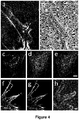
- FIGS 4a and 4b scanning SPC images of an astrocyte obtained by the microscope of Figure 1 are shown.
- images of organelles in embedded astrocytes are obtained by the microscope of Figure 1 respectively in SPC microscopy and confocal fluorescence microscopy, these two images being superposed on Figure 4e .
- images of immunostainded actin filaments are obtained respectively by confocal fluorescence microscopy, STED microscopy implemented by the previously disclosed microscope and confocal SPC implemented by the previously disclosed microscope.
- confocal SPC imaging visualizes weak phase objects.
- Symmetrical alignment of scanning SPC highlights contours of an astrocyte in Vectashield on a dark background.
- Asymmetrical alignment shows the astrocyte with shadow effects on an elevated background like in DIC (differential interference contast).
- the contour detection allows for imaging of organelles in embedded astrocytes.
- Confocal fluorescence imaging of immunostained VAMP3 visualizes vesicles outside organelles.
- SPC and fluorescence images can be perfectly overlayed.
- STED (or confocal fluorescence) images can be recorded simultaneously, since for phase contrast imaging an illumination is used that can be separated easily spectrally from the switch light beam. SPC remains in this case possible although the phase mask is not wavelength matched ( G. situ, G. Pedrini, and W. Osten, J. Opt. Soc. Am. A 26, 1788 (2009 )). True simultaneous imaging eliminates possible registration mismatch due to drift. Spiral phase contrast is implemented in STED microscope without compromising the STED-imaging capabilities. It serves as a valuable second contrast channel, in particular for biological specimen.
- SPC Spiral phase contrast
- the illuminating light source used for phase contrast imaging is arranged on the second side of the objective-lens assembly 3.
- the transfer light source 4b is used as the illuminating light source for phase contrast illumination.
- FIGS 6 , 7 and 8 although shown as comprising a probing light source 4a (Exc Laser) for emitting the excitation beam 5a and a transfer light source 4b (STED Laser) for emitting the laser beam 5b, only one laser device could be used.
- Figure 6 shows the use of the STED beam 5b as the illuminating light beam for phase contrast illumination in transmission mode.
- the microscope 1' according to a second embodiment shown on Figure 6 mainly differs from that of Figure 1 in that the intensity detector 26 (Phase cont. Det) is arranged on the first side of the objective-lens assembly 3 to receive the STED beam 5b having passed successively the phase mask 10, the objective-lens assembly 3 and the sample 2.
- the other parts of the microscope 1' according to the second embodiment are analogous to that already disclosed in relation to the first embodiment. The description will not be repeated and reference is made to the previous description for further details.
- the STED beam 5b is coupled by a lens 30 (L5) into a polarization maintaining fiber 32.
- This arrangement is used to clean the beam profile of the STED beam 5b and to stretch the pulses temporally.
- a lens 31 (L7) serves as output coupler.
- the STED beam 5b passes the phase mask 10, which is imaged by first 11 a and second 11 b lenses (L1 and L2) onto the back focal plane of the objective-lens assembly 3.
- the fluorescent marker is excited in the sample 2 by excitation beam 5a and fluorescence is detected by the probe detector 15 (FL Det). As explained above, fluorescent marker in same regions can be kept dark by the STED beam 5b.
- the light source 4b that emits the STED beam 5b is also used for the illumination beam for the phase contrast:
- the light of the STED light source 4b that has passed the sample 2 is imaged onto the intensity detector 26.
- the illumination light for the phase contrast passes first the phase mask 10 and then the sample 2.
- Figure 7 shows the use of the STED beam 5b for phase contrast illumination together with a retro-reflector.
- the microscope 1" according to a third embodiment shown on Figure 7 mainly differs from that of Figure 1 in that a reflective element 35 is arranged on the first side of the objective-lens assembly 3 at a distance defining a space for placing the sample 2, so as to reflect the STED beam 5b having passed the objective-lens assembly 3.
- the other parts of the microscope 1' according to the second embodiment are analogous to that already disclosed in relation to the first embodiment. The description will not be repeated and reference is made to the previous description for further details.
- the STED beam 5b passes the polarizing beam splitter 24 (BS). Then as in the second embodiment of Figure 6 , the STED beam 5b is coupled by lens 30 (L6) into the polarization maintaining fiber 32. Lens 31 (L7) serves as output coupler.
- the STED beam 5b passes the phase mask 10, which is imaged by first 11 a and second 11 b lenses (L1 and L2) onto the back focal plane of the objective-lens assembly 3.
- a quarter wave plate 37 (QWP) serves for generating circular polarization in the sample 2.
- the fluorescent marker is excited in the sample 2 by excitation beam 5a and fluorescence is detected by the probe detector 15.
- fluorescent marker in same regions can be kept dark by the STED beam 5b.
- the STED beam 5b is reflected back by the retro-reflector 35 consisting of the lens 22 (L4) and a mirror 38 (M), after having passed the sample 2.
- the back-traveling beam carries the phase information form the sample 2 that it passed twice.
- the lens 31 (L7) is focused by the lens 31 (L7) onto the fiber entry which serves as confocal detection pinhole.
- the beam reaches the fiber 32 its polarization is turned by 90° due to the double passage through the quarter wave plate 37.
- the light exits the polarization maintaining fiber therefore also with turned polarization and is reflected by the polarizing beam splitter 24 towards the intensity detector 26.
- other types of retro-reflectors could be used.
- This configuration has the advantage that the STED beam and the confocal phase contrast detection are perfectly aligned because the same fiber (or pinhole) emits the STED beam and serves as confocal pinhole.
- Figure 8 shows the use of the STED beam 5b for phase contrast illumination together with a retro-reflector 35 and beam scanning.
- the microscope 1'" according to a fourth embodiment shown on Figure 8 mainly differs from the third embodiment of Figure 7 in that a scan mirror 40 (SM) allows for scanning the illuminating beam over the sample 2.
- a second telescope 41 consisting of two lenses (L9 and L10) images the scan mirror onto the aperture of the objective-lens assembly 3.
- the other parts of the microscope 1'" according to the fourth embodiment are analogous to that already disclosed in relation to the first embodiment. The description will not be repeated and reference is made to the previous description for further details.
- the above description of the invention has been made with a microscope of Stimulated Emission Depletion (STED) type together with a substance comprising a fluorescent marker.
- the invention is, however, not limited to STED microscopy and could be implemented, more generally, in any other kind of microscopy, such as Reversible Saturable Optical Fluorescence Transitions (RESOLFT) microscopy, in which the switch light beam includes a transfer light beam which, once passed through the wave front modulating optical device, presents a first area with a first intensity adapted to transfer the substance in a second state with second spectral properties to a first state with first spectral properties, and at least a second area with a second intensity adapted not to transfer the substance between the first and second states.
- the substance is chosen accordingly among substances having first and second states of which the respective spectral properties comprise a distinguishing features selected from:
Landscapes
- Physics & Mathematics (AREA)
- Chemical & Material Sciences (AREA)
- Analytical Chemistry (AREA)
- General Physics & Mathematics (AREA)
- Optics & Photonics (AREA)
- Health & Medical Sciences (AREA)
- Nuclear Medicine, Radiotherapy & Molecular Imaging (AREA)
- Life Sciences & Earth Sciences (AREA)
- Biochemistry (AREA)
- General Health & Medical Sciences (AREA)
- Immunology (AREA)
- Pathology (AREA)
- Microscoopes, Condenser (AREA)
- Investigating, Analyzing Materials By Fluorescence Or Luminescence (AREA)
Description
- The invention relates to a microscope for high spatial resolution imaging a structure of interest in a sample.
- Although not limited thereto, the invention especially applies to Stimulated Emission Depletion (STED) microscopy (S. W. Hell and J. Wichmann, Optics Letters 19, 780 (1994); T. A. Klar and S.W. Hell, Optics Letters 24, 954 (1999)) which is an ideal method for imaging with high spatial and temporal resolution. A resolution better than 6 nm (E. Rittweger, K. Y. Han, S. E. Irvine, C. Eggeling, and S. W. Hell, Nature Photonics 3, 144 (2009)) can be reached. STED microscopy allows dynamic imaging (V. Westphal, M. A. Lauterbach, A. Di Nicola, and S. W. Hell, New Journal of Physics 9, 435 (2007)) with up to 200 frames per second (M. A. Lauterbach, C. Ullal, V.Westphal, and S. W. Hell, Langmuir 26, 14400 (2010)) and is compatible with imaging dynamics in living cells (V.Westphal, S. O. Rizzoli, M. A. Lauterbach, D. Kamin, R. Jahn, and S. W. Hell, Science 320, 246 (2008); B. Hein, K. I. Willig, and S. W. Hell, Proceedings of the National Academy of Sciences of the United States of America 105, 14271 (2008)) and even in tissue (U. V. Nägerl, K. I. Willig, B. Hein, S. W. Hell, and T. Bonhoeffer, Proceedings of the National Academy of Sciences of the United States of America 105, 18982 (2008); N. T. Urban, K. I. Willig, S. W. Hell, and U. V. Nägerl, Biophysical Journal 101, 1277 (2011 )). Each of the prior art
US 2011/140000 A1 andUS 2007/206278 A1 teaches an improvement of a microscope for high spatial resolution imaging a structure of interest in a sample as defined by the preamble ofclaim 1. DocumentWO 2010/133678 A1 discloses that a specific STED objective lens could be manufactured with a segmented wave plate already incorporated, similar to lenses for phase contrast microscopy. - A common implementation of STED microscope is as a laser scanning microscope. The sample to image is provided with a substance, such as a fluorescent marker or fluorophores, having a first state with first spectral properties and a second state with second spectral properties. In particular, the fluorophores emit fluorescence when relaxing from the second state to the first state. In STED microscopy, an excitation focus is provided by a focused laser probing light beam illuminating the sample through an objective-lens assembly. The fluorescence ability of the fluorophores in an outer part of the excitation focus is transiently turned off. The switching of the molecules into a non-fluorescent state is achieved via stimulated emission with a laser transfer light beam ("STED beam"). The STED beam is commonly passed through a spiral phase mask of charge one, sometimes imaged with a 4f configuration onto a back focal plane of an objective-lens assembly, resulting in a toroidal focus having a first intensity area with a first intensity adapted to deplete the fluorophores in the second state to the first state, and a second intensity area with a second intensity adapted not to transfer the fluorophores between the first and second states (V. Westphal, M. A. Lauterbach, A. Di Nicola, and S. W. Hell, New Journal of Physics 9, 435 (2007)). Besides, in STED microscopy, fluorescence can be elicited in the stained sample by the probing light beam overlaid onto the STED focus of toroidal ("donut") shape, at least partly onto the second intensity area. Thus, the ability of the fluorophores to emit is turned off via stimulated emission in the first intensity area corresponding to the periphery of the excitation focus. Only in the second area, at the very center, where the STED focus has close-to-zero intensity, the fluorophores are able to spend significant time in the fluorescent state. The second intensity area wherein the fluorophores are not switched off, and accordingly the minimally resolvable distance, shrink to zero with increasing intensity of the STED beam (S. W. Hell, Science 316, 1153 (2007)). The fluorescence of the fluorophores in the second area of the transfer light beam forms an optical measurement signal detected point by point by a probe detector.
- It is, however, often desirable to locate and image structures of interest in a biological specimen as sample, such as cells, which do not strongly absorb light and do not fluoresce. Such structure of interest can hardly be located and imaged using STED microscopy even with the implementation of a second high-resolution color channel.
- The invention aims to solve the above mentioned problem.
- To that end, the invention proposes a microscope for high spatial resolution imaging a structure of interest in a sample comprising a substance as defined by
claim 1. - Hence, the invention provides a high-resolution microscope with improved observation capabilities enabling, through a second contrast channel, to locate and image structures of interest, and especially biological structures of interest, which do not strongly absorb light and do not fluoresce.
- Besides, in accordance with the invention, the phase contrast microscopy system uses the same light beam modulating device as used for the high spatial resolution microscopy system, so that only few optical elements are added, thereof none in the transfer light beam path.
- In addition, using phase contrast for the second contrast channel eliminates necessity for staining the specimen with a second marker.
- The light beam modulating device may be adapted to vary the transfer light beam so that the first intensity area surrounds the second intensity area.
- The light beam modulating device may be a phase mask adapted to modulate the phase profiles of the transfer light beam and of the illuminating light beam.
- In particular, the light beam modulating device may be a spiral phase mask adapted to apply an angular-dependent phase shift to the phase profiles of the transfer light beam and of the illuminating light beam. With these provisions, spiral phase contrast (SPC) (J. Davis, D. McNamara, D. Cottrell, and J. Campos, Optics Letters 25, 99 (2000); S. Fürhapter, A. Jesacher, S. Bernet, and M. Ritsch-Marte, Optics Express 13, 689 (2005)) using the same type of phase mask as is commonly used for shaping a STED beam can be implemented. When used for high spatial resolution imaging, a toroïdal ("donut") shape can be imparted to the transfer light beam passing through the spiral phase mask, resulting in a tubular first intensity area surrounding the second intensity area. When used for phase contrast microscopy, the spiral phase mask provides locations of destructive interference enabling an enhanced signal to noise ratio.
- In a particular embodiment, the microscope may be adapted for Stimulated Emission Depletion (STED) microscopy. In such embodiment, the substance comprises a fluorescent marker emitting fluorescence when relaxing from the second state to the first state, the microscope further comprising a probing light source adapted to emit a probing light beam overlaid with the transfer light beam, said probing light beam having an intensity adapted to transfer the marker in the first state to the second state, the transfer light beam in the first intensity area being adapted to deplete the second state of the marker.
- The transfer light beam and the probing light beam can be emitted by a same sole light source. The transfer light source and the probing light source may form a single light source which produces both transfer and probing light beams.
- As a variant, the transfer light source and the probing light source can be distinct.
- Besides, the transfer light beam and the probing light beam can both pass through the light beam modulating device.
- The microscope may further comprise a transfer light scanning arrangement adapted to move the transfer light beam and the sample relative to each other so that the sample can be scanned by the transfer light beam.
- The microscope may further comprise an illuminating light scanning arrangement adapted to move the illuminating light beam and the sample relative to each other so that the sample can be scanned by the illuminating light beam.
- In an embodiment, the transfer light scanning arrangement may be also used as illuminating light scanning arrangement.
- The intensity detector may be a pixelated detector, such as a CCD or CMOS camera.
- In an alternative, the intensity detector may be a single pixel detector, such as an avalanche photo-diode or a photomultiplier. This provision, in combination with the use of an illuminating light scanning arrangement, enables to perform phase contrast microscopy in a scanning mode. In such scanning mode, phase contrast imaging and high-resolution imaging may use the same scanning arrangement so that image registration depends only on the registration of point sources and detectors, but no image distortions can occur and images can therefore be expected to be well aligned.
- The illuminating light source may comprise a coherent light source, such as a laser device. This provision, in combination with the use of point detector as intensity detector, enables to provide optical sectioning, that is signal removal from planes out of focus.
- In an alternative, the illuminating light source may comprise an incoherent light source, such as a light-emitting diode, a mercury vapour lamp or a halogen lamp.
- The illuminating light source may be arranged on the first side of the objective-lens assembly at a distance defining a space for placing the sample.
- The intensity detector may then be arranged on the second side of the objective-lens assembly.
- In an alternative, the illuminating light source may be arranged on the second side of the objective-lens assembly.
- A reflective element may be arranged on the first side of the objective-lens assembly at a distance defining a space for placing the sample.
- In a variant, the intensity detector may be arranged on the first side of the objective-lens assembly.
- In particular, the transfer light beam may be the illuminating light beam.
- Other objects and advantages of the invention will emerge from the following disclosure of particular embodiments of the invention given as non limitative example, the disclosure being made in reference to the enclosed drawings in which:
-
Figure 1 is a sketch of the main elements of a microscope for high spatial resolution imaging according to a first embodiment of the invention, the microscope implementing an objective-lens assembly, a light source emitting a transfer light beam and a probing light beam, a phase mask and a probe detector for high spatial resolution imaging, and an illuminating light source and an intensity detector for phase contrast imaging, -
Figures 2 are phase contrast images obtained by the microscope ofFigure 1 of a sample consisting of small immersion oil droplets on a coverslip, with different positions of the phase mask with respect to an illuminating light beam emitted by the illuminating light source having passed through the sample (A, B, C), and four possible illumination/scanning combinations: incoherent illuminating light beam/wide-field detection (D), incoherent illuminating light beam/scanning detection (E), coherent illuminating light beam/wide-field detection (F), coherent illuminating light beam/scanning detection (G), -
Figure 3 shows (a) a phase contrast image of neurons obtained by the microscope ofFigure 1 with incoherent illumination and wide-field detection, (b) a phase contrast image of neurons obtained by the microscope ofFigure 1 with incoherent illumination and scanning detection, (c) an image of a region of interest selected from the phase contrast images obtained by a conventional confocal fluorescence microscopy and (d, e) STED images of the region of interest obtained by the microscope ofFigure 1 , -
Figure 4 shows (a, b) scanning SPC images of an astrocyte obtained by the microscope ofFigure 1 , (c) an SPC image of organelles in embedded astrocytes obtained by the microscope ofFigure 1 , (d) a STED image of organelles in embedded astrocytes obtained by the microscope ofFigure 1 , (c) a superposition of the SPC and STED images of organelles in embedded astrocytes obtained by the microscope ofFigure 1 , (f) a confocal fluorescence image of immunostainded actin filaments, (g) a STED image of immunostainded actin filaments obtained by the microscope ofFigure 1 , (h) confocal SPC image of immunostainded actin filaments obtained by the microscope ofFigure 1 , -
Figure 5 is a sketch of the main elements of a microscope for high spatial resolution imaging according to a variant of the embodiment ofFigure 1 , wherein the transfer light beam and the probing light beam are emitted by two distinct light sources, -
Figure 6 is a sketch of the main elements of a microscope for high spatial resolution imaging according to a second embodiment of the invention, wherein the transfer light source is also used as illuminating light source for phase contrast in transmission mode, -
Figure 7 is a sketch of the main elements of a microscope for high spatial resolution imaging according to a third embodiment of the invention, wherein the transfer light source is also used as illuminating light source for phase contrast together with a retro-reflector, -
Figure 8 is a sketch of the main elements of a microscope for high spatial resolution imaging according to a fourth embodiment of the invention, wherein the switch light source is also used as illuminating light source for phase contrast together with a retro-reflector and beam scanning. - On the Figures, the same reference numbers refer to the same or similar elements.
-
Figure 1 illustrates amicroscope 1 for high spatial resolution imaging especially adapted for locating and imaging biological structures of interest, such as biological cells, in a sample 2 (SMP). - In
Figure 1 , a Stimulated Emission Depletion (STED)microscope 1 is represented for imaging a structure of interest marked with a fluorescent marker as a substance having a first state with first spectral properties and a second state with second spectral properties. Actually, the fluorescent marker can be repeatedly transferred from a ground state as first state to an excited state as second state, and emits fluorescence when relaxing from the excited state to the ground state. - The
microscope 1 comprises an objective-lens assembly 3 (OBJ) having a first or front side and a second or back side, the front and back sides being opposite to each other. On the front side, the objective-lens assembly 3 presents a first or front focal plane in which thesample 2 to be imaged is placed. A second or back focal plane is arranged on the back side of the objective-lens assembly 3. - A
light source 4 comprising a transfer light source is arranged on the second side of the objective-lens assembly 3 to emit alight beam 6 towards thesample 2 through the objective-lens assembly 3. - In the illustrated embodiment, the
light source 4 comprises a sole laser device adapted to emit thelaser beam 6, such as a Ti:Sapphire laser Ti:Sa, and aseparator 7 for separating thelaser beam 6 into a probinglight beam 5a and atransfer light beam 5b. The probinglight beam 5a is adapted, especially in terms of intensity and wavelength, for causing an excitation of the fluorescent marker and transferring the fluorescent marker from the ground state to the excited state. Conversely, thetransfer light beam 5b is adapted, especially in terms of intensity and wavelength, for causing a de-excitation of the fluorescent marker and depletion of the excited state of the fluorescent marker to the ground state. - In a variant shown on
Figure 5 , the probinglight beam 5a and thetransfer light beam 5b can be emitted separately, respectively by two distinct transfer light (4b) and probing light (4a) sources. - In particular, the laser device pumps an frequency doubled
OPO 8 to generate thetransfer light beam 5b, or a STED beam in the present embodiment, and a photonic-crystal fiber 9 (PCF) to generate the probinglight beam 5a, or a supercontinuum for excitation in the present embodiment. A dielectric filter can be used to select the excitation wavelength. Generation ofSTED 5b andexcitation 5a beams from the same source eliminates potential time jitter (E. Auksorius, B. R. Boruah, C. Dunsby, P. M. P. Lanigan, G. Kennedy, M. A. A. Neil, and P. M. W. French, Optics Letters 33, 113 (2008)). Temporal overlay of the pulsed is adjusted with an optical delay line (not shown). - The
STED beam 5b is directed towards the objective-lens assembly 3 through a lightbeam modulating device 10 placed on the second side of the objective-lens assembly 3, between thelight source 4 and the objective-lens assembly 3. - The light
beam modulating device 10 is adapted to spatially vary theSTED beam 5b, and especially its intensity and/or its phase, so that, once theSTED beam 5b has passed trough the lightbeam modulating device 10 and the objective-lens assembly 3, it presents at least a first intensity area with the nominal intensity adapted to transfer the fluorescent marker in the excited state to the ground state, and at least a second intensity area with a second intensity adapted not to transfer the fluorescent marker between the first and second states. In particular, the second intensity area can have a zero or close-to-zero intensity. - In a preferred embodiment, although not limited thereto, the light
beam modulating device 10 is a spiral phase mask (PM) adapted to apply an angular-dependent phase shift to a phase profile of theSTED beam 5b. For example, suchspiral phase mask 10 may consist of a reflective or transmissive plate extending generally perpendicularly to the optical axis and presenting to opposite transverse surfaces at least one of which being helical around the optical axis. Suchspiral phase mask 10 is able to generate a toroidal focus of theSTED beam 5b so that so that the first intensity area of the intensity suitable for depletion of the excited state of the fluorescent marker continuously surrounds the second intensity area of zero or close-to-zero intensity. - In other embodiments, the light
beam modulating device 10 could be any other kind of phase mask adapted to modulate or change the phase profile of the transfer light beam, preferably so that the first intensity area at least partly surrounds the second intensity area. The lightbeam modulating device 10 could also be any other spatial light modulator. - A
telescope 11 comprising first 11 a and second 11 b lenses (L1 and L2) in 4f configuration images the back focal plane of the objective-lens assembly 3 onto thephase mask 10 in order to have thephase mask 10 in the Fourier plane of the objective-lens assembly 3. - The
STED beam 5b passes thespiral phase mask 10 to generate the toroidal focus in thesample 2. Theexcitation beam 5a is combined with theSTED beam 5b so as to be overlaid with at least with a part of the second area of theSTED beam 5b through a first dichroic mirror 12 (DM1). Theexcitation 5a andSTED 5b beams thereby form aswitch light beam 5 illuminating thesample 2. - The
microscope 1 further comprises a transfer light scanning arrangement adapted to move at least thetransfer light beam 5b and thesample 2 relative to each other so that thesample 2 can be scanned by theswitch light beam 5. In a variant, the transfer light scanning arrangement may move both thetransfer 5b and probing 5a light beams formingswitch light beam 5 and thesample 2 relative to each other. The transfer light scanning arrangement can comprise a scanner adapted to change the orientation of thetransfer light beam 5b (of the switch light beam 5) and/or a movable support on which thesample 2 is mounted. In the illustrated embodiment, the sample is scanned with a piezo stage. - In doing so, at the center of the
switch light beam 5, the fluorescence of the fluorescent marker can be elicited by theexcitation beam 5a overlaid onto the zero or close-to-zero intensity area of theSTED beam 5b. On the contrary, at the periphery of theswitch light beam 5, the ability of the fluorescent marker to emit is turned off via stimulated emission by the tubular first intensity area of theSTED beam 5b. - The
switch light beam 5 is separated from fluorescence with a second dichroic mirror 13 (DM2). Aprobe detector 15, such as an avalanche photo diode (APD), is arranged on the second side of the objective-lens assembly 3 to detect the fluorescence of the fluorescent marker as an optical measurement signal. - According to the invention, the above disclosed
STED microscope 1 implements spiral phase contrast (SPC). - To that end, the
microscope 1 further comprises an illuminatinglight source 16 arranged to emit an illuminatinglight beam 17 towards thesample 2 from the first side of the objective-lens assembly 3. - On
Figure 1 , the illuminatinglight source 16 is arranged on the first side of the objective-lens assembly 3 at a distance defining a space for placing thesample 2. The illuminatinglight source 16 comprises an incoherentlight source 18, such as a light-emitting diode 19 (LED) (wavelength 630 nm) arranged behind aplate 20 provided with an aperture (pinhole PH) for Köhler illumination. In a variant, the incoherentlight source 18 could be mercury vapour lamp, a halogen lamp or other. A lens 21 (L5) serves as collector and a lens 22 (L4) focuses the illuminatinglight beam 17 onto thesample 2. In the illustrated embodiment, the illuminatinglight source 16 also comprises a coherentlight source 23, such as a laser device. Thesample 2 can be illuminated with either of the incoherent 18 and coherent 23 light sources. In alternatives, the illuminatinglight source 16 could comprise only one of the incoherent 18 and coherent 23 light sources. - The
phase mask 10 is placed in the Fourier plane of the objective-lens assembly 3 for an isotropic contrast enhancement for amplitude and phase objects. It was demonstrated that SPC with coherent laser illumination allows visualizing weak phase objects such as cells (A. Jesacher, S. Fürhapter, S. Bernet, and M. Ritsch-Marte, Physical Review Letters 94 (2005)). Recently a LED, with a spectrum filtered to 1 nm was used to image biological specimen (G. Situ, M. Warber, G. Pedrini, and W. Osten, Optics Communications 283, 1273 (2010)) and SPC with a superluminescent diode was demonstrated (S. Schausberger, B. Heise, C. Maurer, S. Bernet, M. Ritsch-Marte, and D. Stifter, )). - A polarizing beam splitter 24 (PBS) arranged on the second side of the objective-
lens assembly 3 separates theSTED beam 5b and thephase contrast beam 17a composed of the illuminatinglight beam 17 having passed through thesample 2, the objective-lens assembly 3 and thephase mask 10. - A Lens 25 (L3) forms the phase contrast image on an intensity detector 26 (Det) arranged on the second side of the objective-
lens assembly 3 to detect an intensity of thephase contrast beam 17a. - The
intensity detector 26 can be a pixelated detector, such as a CCD or CMOS camera, to enable wide-field detection. - In a preferred variant, the
intensity detector 26 can be a single pixel detector, such as an avalanche photo-diode or a photomultiplier. Advantageously, themicroscope 1 may then further comprise an illuminating light scanning arrangement adapted to move the illuminatinglight beam 17 and thesample 2 relative to each other so that thesample 2 can be scanned by the illuminatinglight beam 17. As for the switch light scanning arrangement, illuminating light scanning arrangement can comprise a scanner adapted to change the orientation of the illuminatinglight beam 17 and/or the movable support on which thesample 2 is mounted. Such provisions enable implementation of SPC in a scanning mode. As it will become apparent from the following of the description, illuminating light scanning arrangement can be formed by the transfer light scanning arrangement. - In the disclosed embodiment, the implemented phase contrast modality is of spiral type thanks to the use of a
spiral phase mask 10 in the STED microscope. Any other type of phase contrast modality could, however, be implemented depending on thephase mask 10, and more generally the light beam modulating device, of the high resolution microscope. - A characterization of SPC itself is shown on
Figure 2 in which small immersion oil droplets on a coverslip, which give a strong phase contrast, were used as test sample. The same region of interest was recorded with the four possible illumination/scanning combinations: incoherent LED illumination, wide-field detection (Figure 2D ); incoherent LED illumination, scanning detection (Figure 2E ); coherent laser illumination, wide-field detection (Figure 2F ); coherent laser illumination, scanning detection (Figure 2G ). Also the position of the phase mask with respect to the illuminating beam of a coherent illumination was studied (Figures 2A, 2B and 2C ). - On
Figures 2A, 2B and 2C , it is shown that coherent illumination (laser) leads to spirals, whose starting point depends on the slight de-centering of the phase mask. The starting point of the spirals with coherent illumination depends on this position. If the singularity and, in the present case, the helical shape of the plate, of the phase mask is centered on the illuminating beam, the spiral phase contrast does not lead to spiral but to its degenerate from, concentric rings (Figure 2A ). Slightly offsetting the phase mask leads to spirals, whose starting points depend on the phase mask position (Figures 2B and 2C ). - On
Figures 2D, 2E, 2F and 2G , comparing wide-field and scanning modes, for incoherent illumination (LED), essentially no differences are seen (Figures 2D and 2E ). In contrast, coherent illumination (laser) leads in wide-field configuration to strong background of interference fringes originating from reflections on various surfaces in the optical path (Figure 2F ). In scanning configuration, this background is more homogeneous and constant irrespective of the sample position because shadows that do not originate from the sample are constant over the whole image, so that the image quality is improved in scanning configuration (Figure 2G ). A constant offset in the images is removed for display (contrast stretching), but images are not saturated. Scanned images were recorded with 50 nm pixels. - On
Figures 3a and 3b , phase contrast images of neurons obtained by the above disclosed microscope are shown. OnFigure 3a , the image is obtained with incoherent illumination and wide-field detection, whereas onFigure 3b , the image is obtained with incoherent illumination and scanning detection. OnFigure 3c , an image obtained by a conventional confocal fluorescence microscopy of a region of interest selected from the phase contrast images ofFigures 3a and 3b is shown. OnFigures 3d and 3e , an image of the same region of interest obtained by high-resolution STED microscopy with the previously disclosed microscope is shown, noise having been suppressed by Wiener filtering onFigure 3e (onFigure 3d , the inset shows an intensity profile according to the white bar). - As can be seen on
Figure 3 , wide-field and scanning SPC may clearly visualizes neurons including flat details such as neuritis and allows for the selection of a region of interest to be imaged in conventional confocal fluorescence microscopy or in high-resolution STED microscopy. - On
Figures 4a and 4b , scanning SPC images of an astrocyte obtained by the microscope ofFigure 1 are shown. OnFigures 4c and 4d , images of organelles in embedded astrocytes are obtained by the microscope ofFigure 1 respectively in SPC microscopy and confocal fluorescence microscopy, these two images being superposed onFigure 4e . Onfigures 4f, 4g and 4h , images of immunostainded actin filaments are obtained respectively by confocal fluorescence microscopy, STED microscopy implemented by the previously disclosed microscope and confocal SPC implemented by the previously disclosed microscope. - As can be seen on
Figure 4 , confocal SPC imaging visualizes weak phase objects. (a) Symmetrical alignment of scanning SPC highlights contours of an astrocyte in Vectashield on a dark background. (b) Asymmetrical alignment shows the astrocyte with shadow effects on an elevated background like in DIC (differential interference contast). (c) The contour detection allows for imaging of organelles in embedded astrocytes. (d) Confocal fluorescence imaging of immunostained VAMP3 visualizes vesicles outside organelles. (e) SPC and fluorescence images can be perfectly overlayed. (f) Immunostainded actin filaments in the fine protrusions of the neuronal growth cone of a neurone (confocal fluorescence imaging). (g) STED imaging allows resolving details of the actin organization. (g) Confocal SPC (green) enables visualizing the fine protrusions in phase contrast. The symmetrical contour detection suits for an overlay with the STED image (red). Scale bars: (b) 5 µm; (e) 10 µm; (h) 0.5 µm. - With the microscope of the invention, STED (or confocal fluorescence) images can be recorded simultaneously, since for phase contrast imaging an illumination is used that can be separated easily spectrally from the switch light beam. SPC remains in this case possible although the phase mask is not wavelength matched (G. Situ, G. Pedrini, and W. Osten, J. Opt. Soc. Am. A 26, 1788 (2009)). True simultaneous imaging eliminates possible registration mismatch due to drift. Spiral phase contrast is implemented in STED microscope without compromising the STED-imaging capabilities. It serves as a valuable second contrast channel, in particular for biological specimen.
- Spiral phase contrast (SPC) is incorporated into a
STED microscope 1 with only few additional optical elements. In particular, thesame phase mask 10 shapes theSTED beam 5b and generates the phase contrast. Imaging of cells with two contrast channels, label-free phase contrast and high-resolution STED microscopy can then be performed. - In other embodiments shown on
Figures 6 ,7 and8 , the illuminating light source used for phase contrast imaging is arranged on the second side of the objective-lens assembly 3. In particular, the transferlight source 4b is used as the illuminating light source for phase contrast illumination. Onfigures 6 ,7 and8 , although shown as comprising a probinglight source 4a (Exc Laser) for emitting theexcitation beam 5a and a transferlight source 4b (STED Laser) for emitting thelaser beam 5b, only one laser device could be used. - In particular,
Figure 6 shows the use of theSTED beam 5b as the illuminating light beam for phase contrast illumination in transmission mode. The microscope 1' according to a second embodiment shown onFigure 6 mainly differs from that ofFigure 1 in that the intensity detector 26 (Phase cont. Det) is arranged on the first side of the objective-lens assembly 3 to receive theSTED beam 5b having passed successively thephase mask 10, the objective-lens assembly 3 and thesample 2. The other parts of the microscope 1' according to the second embodiment are analogous to that already disclosed in relation to the first embodiment. The description will not be repeated and reference is made to the previous description for further details. - In this embodiment, the
STED beam 5b is coupled by a lens 30 (L5) into apolarization maintaining fiber 32. This arrangement is used to clean the beam profile of theSTED beam 5b and to stretch the pulses temporally. A lens 31 (L7) serves as output coupler. However, it is not mandatory to use a fiber for cleaning and stretching. For example, for spatial cleaning the fiber could be replaced by a pinhole. TheSTED beam 5b passes thephase mask 10, which is imaged by first 11 a and second 11 b lenses (L1 and L2) onto the back focal plane of the objective-lens assembly 3. - For high-resolution fluorescence imaging, the fluorescent marker is excited in the
sample 2 byexcitation beam 5a and fluorescence is detected by the probe detector 15 (FL Det). As explained above, fluorescent marker in same regions can be kept dark by theSTED beam 5b. - For phase contrast imaging, the
light source 4b that emits theSTED beam 5b is also used for the illumination beam for the phase contrast: The light of the STEDlight source 4b that has passed thesample 2 is imaged onto theintensity detector 26. In contrast to the implementation shown onFigure 1 , the illumination light for the phase contrast passes first thephase mask 10 and then thesample 2. -
Figure 7 shows the use of theSTED beam 5b for phase contrast illumination together with a retro-reflector. Themicroscope 1" according to a third embodiment shown onFigure 7 mainly differs from that ofFigure 1 in that areflective element 35 is arranged on the first side of the objective-lens assembly 3 at a distance defining a space for placing thesample 2, so as to reflect theSTED beam 5b having passed the objective-lens assembly 3. Again, the other parts of the microscope 1' according to the second embodiment are analogous to that already disclosed in relation to the first embodiment. The description will not be repeated and reference is made to the previous description for further details. - The
STED beam 5b passes the polarizing beam splitter 24 (BS). Then as in the second embodiment ofFigure 6 , theSTED beam 5b is coupled by lens 30 (L6) into thepolarization maintaining fiber 32. Lens 31 (L7) serves as output coupler. TheSTED beam 5b passes thephase mask 10, which is imaged by first 11 a and second 11 b lenses (L1 and L2) onto the back focal plane of the objective-lens assembly 3. A quarter wave plate 37 (QWP) serves for generating circular polarization in thesample 2. - As for the second embodiment of
Figure 6 , for high-resolution fluorescence imaging, the fluorescent marker is excited in thesample 2 byexcitation beam 5a and fluorescence is detected by theprobe detector 15. As explained above, fluorescent marker in same regions can be kept dark by theSTED beam 5b. - For phase contrast imaging, the
STED beam 5b is reflected back by the retro-reflector 35 consisting of the lens 22 (L4) and a mirror 38 (M), after having passed thesample 2. Use of a spherical mirror is advantageous but not necessary. The back-traveling beam carries the phase information form thesample 2 that it passed twice. After having passed the phase mask 10 a second time, it is focused by the lens 31 (L7) onto the fiber entry which serves as confocal detection pinhole. When the beam reaches thefiber 32 its polarization is turned by 90° due to the double passage through thequarter wave plate 37. The light exits the polarization maintaining fiber therefore also with turned polarization and is reflected by thepolarizing beam splitter 24 towards theintensity detector 26. In variants, other types of retro-reflectors could be used. - This configuration has the advantage that the STED beam and the confocal phase contrast detection are perfectly aligned because the same fiber (or pinhole) emits the STED beam and serves as confocal pinhole.
-
Figure 8 shows the use of theSTED beam 5b for phase contrast illumination together with a retro-reflector 35 and beam scanning. The microscope 1'" according to a fourth embodiment shown onFigure 8 mainly differs from the third embodiment ofFigure 7 in that a scan mirror 40 (SM) allows for scanning the illuminating beam over thesample 2. Asecond telescope 41 consisting of two lenses (L9 and L10) images the scan mirror onto the aperture of the objective-lens assembly 3. Again, the other parts of the microscope 1'" according to the fourth embodiment are analogous to that already disclosed in relation to the first embodiment. The description will not be repeated and reference is made to the previous description for further details. - The above description of the invention has been made with a microscope of Stimulated Emission Depletion (STED) type together with a substance comprising a fluorescent marker. The invention is, however, not limited to STED microscopy and could be implemented, more generally, in any other kind of microscopy, such as Reversible Saturable Optical Fluorescence Transitions (RESOLFT) microscopy, in which the switch light beam includes a transfer light beam which, once passed through the wave front modulating optical device, presents a first area with a first intensity adapted to transfer the substance in a second state with second spectral properties to a first state with first spectral properties, and at least a second area with a second intensity adapted not to transfer the substance between the first and second states. The substance is chosen accordingly among substances having first and second states of which the respective spectral properties comprise a distinguishing features selected from:
- an altered optical absorption of a probe beam,
- an altered polarization property for a probe beam,
- an altered luminescence selected from fluorescence, phosphorescence, electroluminescence and chemo-luminescence.
Claims (18)
- A microscope (1; 1'; 1"; 1'") for high spatial resolution imaging a structure of interest in a sample (2) comprising a substance, said substance having a first state with first spectral properties and a second state with second spectral properties, the microscope (1; 1'; 1 "; 1'") comprising:- an objective-lens assembly (3) having first and second sides opposite to each other, and presenting first and second focal planes respectively on said first and second sides, the sample (2) being intended to be placed on the first side,- a transfer light source (4,4b) arranged on the second side of the objective-lens assembly (3) to emit a transfer light beam (5b) towards the sample (2) through the objective-lens assembly (3), said transfer light beam (5b) having an intensity and a phase profile,- a light beam modulating device (10) placed between the transfer light source (4,4b) and the objective-lens assembly (3), said light beam modulating device (10) being adapted to spatially vary the transfer light beam (5b) so that said transfer light beam (5b) after having passed trough said light beam modulating device (10) and the objective-lens assembly (3) presents at least a first intensity area with a first intensity adapted to transfer the substance in the second state to the first state, and at least a second intensity area with a second intensity adapted not to transfer the substance between the first and second states,- a probe detector (15) adapted to detect an optical measurement signal from a portion of the substance in the second state,said microscope (1; 1'; 1"; 1'") being characterised in that it comprises a phase contrast microscopy system which includes:- the light beam modulating device (10) further adapted to generate a phase contrast,- an illuminating light source arranged to emit an illuminating light beam (17; 5b) towards the sample (2), wherein said illuminating light source either coincides with the transfer light source (4,4b) or is a separate light source (16), said illuminating light beam (17; 5b) having an intensity and a phase profile,- an intensity detector (26) arranged to detect the intensity of the illuminating light beam (17; 5b) after said illuminating light beam (17; 5b) has passed at least once through the sample (2), the objective lens assembly (3) and the light beam modulating device (10).
- Microscope (1; 1'; 1"; 1'") according to claim 1, wherein the light beam modulating device (10) is adapted to vary the transfer light beam (5b) so that the first intensity area surrounds the second intensity area.
- Microscope (1; 1'; 1"; 1'") according to claim 1 or 2, wherein the light beam modulating device (10) being a phase mask adapted to modulate the phase profiles of the transfer light beam (5b) and of the illuminating light beam (17; 5b).
- Microscope (1; 1'; 1"; 1'") according to claim 3, wherein the light beam modulating device (10) is a spiral phase mask adapted to apply an angular-dependent phase shift to the phase profiles of the transfer light beam (5b) and of the illuminating light beam (17; 5b).
- Microscope (1; 1'; 1"; 1'") according to any of claims 1 to 4, wherein the substance comprises a fluorescent marker emitting fluorescence when relaxing from the second state to the first state, the microscope further comprising a probing light source (4a) adapted to emit a probing light beam (5a) overlaid with the transfer light beam (5b), said probing light beam (5a) having an intensity adapted to transfer the marker in the first state to the second state, the transfer light beam (5b) in the first intensity area being adapted to deplete the second state of the marker.
- Microscope (1) according to claim 5, wherein the transfer light source (4b) and the probing light source (4a) form a single light source (4) which produces both transfer (5b) and probing (5a) light beams.
- Microscope (1; 1'; 1 "; 1'") according to any of claims 1 to 6, further comprising a transfer light scanning arrangement adapted to move the transfer light beam (5b) and the sample (2) relative to each other so that the sample (2) can be scanned by the transfer light beam (5b).
- Microscope (1; 1'; 1 "; 1'") according to any of claims 1 to 7, further comprising an illuminating light scanning arrangement adapted to move the illuminating light beam (17; 5b) and the sample (2) relative to each other so that the sample (2) can be scanned by the illuminating light beam (17; 5b).
- Microscope (1; 1'; 1"; 1'") according to any of claims 1 to 8, wherein the intensity detector (26) is a pixelated detector, such as a CCD or CMOS camera.
- Microscope (1; 1'; 1"; 1'") according to any of claims 1 to 8, wherein the intensity detector (26) is a single pixel detector, such as an avalanche photo-diode or a photomultiplier.
- Microscope (1; 1'; 1"; 1'") according to any of claims 1 to 10, wherein the illuminating light source (16; 4b) comprises a coherent light source, such as a laser device.
- Microscope (1) according to any of claims 1 to 10, wherein the illuminating light source (16) comprises an incoherent light source, such as a light-emitting diode, a mercury vapour lamp or a halogen lamp.
- Microscope (1) according to any of claims 1 to 12, wherein the illuminating light source (16) is arranged on the first side of the objective-lens assembly (3) at a distance defining a space for placing the sample (2).
- Microscope (1) according to claim 13, wherein the intensity detector (26) is arranged on the second side of the objective-lens assembly (3).
- Microscope (1'; 1"; 1'") according to any of claims 1 to 12, wherein the illuminating light source (4b) is arranged on the second side of the objective-lens assembly (3).
- Microscope (1'; 1"; 1'") according to claim 15, wherein a reflective element (35) is arranged on the first side of the objective-lens assembly (3) at a distance defining a space for placing the sample (2).
- Microscope (1') according to claim 15, wherein the intensity detector (26) is arranged on the first side of the objective-lens assembly (3).
- Microscope (1'; 1"; 1'") according to any of claims 15 to 17, wherein the transfer light beam (5b) is the illuminating light beam (17; 5b).
Priority Applications (1)
| Application Number | Priority Date | Filing Date | Title |
|---|---|---|---|
| EP13722347.5A EP2847632B1 (en) | 2012-05-07 | 2013-05-03 | Microscope for high spatial resolution imaging a structure of interest in a sample |
Applications Claiming Priority (3)
| Application Number | Priority Date | Filing Date | Title |
|---|---|---|---|
| EP12305509 | 2012-05-07 | ||
| PCT/EP2013/059230 WO2013167479A1 (en) | 2012-05-07 | 2013-05-03 | Microscope for high spatial resolution imaging a structure of interest in a sample |
| EP13722347.5A EP2847632B1 (en) | 2012-05-07 | 2013-05-03 | Microscope for high spatial resolution imaging a structure of interest in a sample |
Publications (2)
| Publication Number | Publication Date |
|---|---|
| EP2847632A1 EP2847632A1 (en) | 2015-03-18 |
| EP2847632B1 true EP2847632B1 (en) | 2017-05-03 |
Family
ID=48430707
Family Applications (1)
| Application Number | Title | Priority Date | Filing Date |
|---|---|---|---|
| EP13722347.5A Active EP2847632B1 (en) | 2012-05-07 | 2013-05-03 | Microscope for high spatial resolution imaging a structure of interest in a sample |
Country Status (4)
| Country | Link |
|---|---|
| US (1) | US9348128B2 (en) |
| EP (1) | EP2847632B1 (en) |
| JP (1) | JP6255389B2 (en) |
| WO (1) | WO2013167479A1 (en) |
Families Citing this family (10)
| Publication number | Priority date | Publication date | Assignee | Title |
|---|---|---|---|---|
| US9500586B2 (en) * | 2014-07-24 | 2016-11-22 | Nxgen Partners Ip, Llc | System and method using OAM spectroscopy leveraging fractional orbital angular momentum as signature to detect materials |
| US20160015264A1 (en) * | 2014-07-17 | 2016-01-21 | Samsung Electronics Co., Ltd. | Imaging system and method for diagnostic imaging |
| US10161870B2 (en) | 2015-10-05 | 2018-12-25 | Nxgen Partners Ip, Llc | System and method for multi-parameter spectroscopy |
| US11703800B2 (en) | 2018-03-21 | 2023-07-18 | The Board Of Trustees Of The Leland Stanford Junior University | Methods for temporal and spatial multiplexing of spatial light modulators and systems for same |
| PT110747B (en) * | 2018-05-18 | 2023-02-10 | Inst De Biologia Molecular E Celular Ibmc | DEVICE TO IMPROVE PERFORMANCE IN MICROSCOPY BY STIMULATED EMISSION DEPLETION (STED) USING A SINGLE PHASE MASK |
| CN109683312B (en) * | 2019-01-22 | 2021-03-12 | 中国工程物理研究院激光聚变研究中心 | Method for adjusting image transfer relationship of adaptive optical system |
| EP3686643A1 (en) * | 2019-01-25 | 2020-07-29 | Hochschule Für Angewandte Wissenschaften München | Pulse shaping for stimulated emission depletion microscopy |
| DE102019008304B8 (en) * | 2019-11-29 | 2021-06-02 | Abberior Instruments Gmbh | Fluorescence microscope with stabilized adjustment and use of an assembly to upgrade a fluorescence microscope |
| DE102019135033A1 (en) | 2019-12-19 | 2021-06-24 | Friedrich-Schiller-Universität Jena | Creation of a light field with several localized zeros |
| DE102021128556A1 (en) | 2021-11-03 | 2023-05-04 | Amphos GmbH | STED microscope |
Family Cites Families (8)
| Publication number | Priority date | Publication date | Assignee | Title |
|---|---|---|---|---|
| JP2006220994A (en) * | 2005-02-10 | 2006-08-24 | Olympus Corp | Observation system |
| US7679741B2 (en) * | 2006-03-01 | 2010-03-16 | Leica Microsystems Cms Gmbh | Method and microscope for high spatial resolution examination of samples |
| DE102007025688A1 (en) * | 2007-06-01 | 2008-12-11 | MAX-PLANCK-Gesellschaft zur Förderung der Wissenschaften e.V. | Wavelength- or polarization-sensitive optical design and its use |
| DE102007039111B4 (en) * | 2007-08-18 | 2014-11-20 | MAX-PLANCK-Gesellschaft zur Förderung der Wissenschaften e.V. | STED fluorescence microscopy with two-photon excitation |
| US8174692B2 (en) * | 2008-05-21 | 2012-05-08 | Max-Planck-Gesellschaft Zur Foerderung Der Wissenschaften E.V. | High spatial resolution imaging of a structure of interest in a specimen |
| US20100252750A1 (en) * | 2009-04-03 | 2010-10-07 | Xiaoliang Sunney Xie | Systems and methods for stimulated emission imaging |
| DE202009007250U1 (en) * | 2009-05-20 | 2009-11-26 | Deutsches Krebsforschungszentrum Stiftung des öffentlichen Rechts | Field changing means for generating complementary light intensity patterns |
| JP5484879B2 (en) * | 2009-12-11 | 2014-05-07 | オリンパス株式会社 | Super-resolution microscope |
-
2013
- 2013-05-03 JP JP2015510752A patent/JP6255389B2/en active Active
- 2013-05-03 EP EP13722347.5A patent/EP2847632B1/en active Active
- 2013-05-03 WO PCT/EP2013/059230 patent/WO2013167479A1/en not_active Ceased
- 2013-05-03 US US14/394,009 patent/US9348128B2/en active Active
Also Published As
| Publication number | Publication date |
|---|---|
| EP2847632A1 (en) | 2015-03-18 |
| JP6255389B2 (en) | 2017-12-27 |
| US20150076333A1 (en) | 2015-03-19 |
| JP2015517681A (en) | 2015-06-22 |
| WO2013167479A1 (en) | 2013-11-14 |
| US9348128B2 (en) | 2016-05-24 |
Similar Documents
| Publication | Publication Date | Title |
|---|---|---|
| US9348128B2 (en) | Microscope for high spatial resolution imaging a structure of interest in a sample | |
| Sanderson et al. | Fluorescence microscopy | |
| US8362448B2 (en) | Apparatus and method for high spatial resolution imaging of a structure of a sample | |
| Gregor et al. | Image scanning microscopy | |
| US8705172B2 (en) | Microscopy method and microscope with enhanced resolution | |
| US8217992B2 (en) | Microscopic imaging techniques | |
| US20130015370A1 (en) | Confocal fluorescence slide scanner with parallel detection | |
| US20070206278A1 (en) | Method and microscope for high spatial resolution examination of samples | |
| CA3013946A1 (en) | Method and system for improving lateral resolution in optical scanning microscopy | |
| US9404867B2 (en) | Luminescence microscopy | |
| JP2010092002A (en) | Optical microscope | |
| CA2978123A1 (en) | Real time multichannel sted microscopy system | |
| JP2012237647A (en) | Multifocal confocal raman spectroscopic microscope | |
| US20050006597A1 (en) | Arrangement for the optical detection of light radiation which is excited and/or backscattered in a specimen with a double-objective arrangement | |
| JP2022520996A5 (en) | ||
| Jonkman et al. | [18] Resolution in optical microscopy | |
| Lee | Progresses in implementation of STED microscopy | |
| Wang et al. | High-spatiotemporal-resolution structured illumination microscopy: principles, instrumentation, and applications | |
| WO2017094184A1 (en) | Scanning microscope and microscope image acquisition method | |
| JPH10142151A (en) | Light microscope | |
| JPWO2017158697A1 (en) | Image acquisition method and image acquisition apparatus | |
| Ordóñez et al. | Single-pixel fluorescence microscopy with optical sectioning | |
| Macháň | Introduction to Fluorescence Microscopy | |
| JP6806161B2 (en) | Microscope system | |
| KR101592898B1 (en) | Combined spatially chirped modulation and spectral encoding for confocal reflectance microscopy |
Legal Events
| Date | Code | Title | Description |
|---|---|---|---|
| PUAI | Public reference made under article 153(3) epc to a published international application that has entered the european phase |
Free format text: ORIGINAL CODE: 0009012 |
|
| 17P | Request for examination filed |
Effective date: 20141008 |
|
| AK | Designated contracting states |
Kind code of ref document: A1 Designated state(s): AL AT BE BG CH CY CZ DE DK EE ES FI FR GB GR HR HU IE IS IT LI LT LU LV MC MK MT NL NO PL PT RO RS SE SI SK SM TR |
|
| AX | Request for extension of the european patent |
Extension state: BA ME |
|
| DAX | Request for extension of the european patent (deleted) | ||
| 17Q | First examination report despatched |
Effective date: 20151204 |
|
| GRAP | Despatch of communication of intention to grant a patent |
Free format text: ORIGINAL CODE: EPIDOSNIGR1 |
|
| STAA | Information on the status of an ep patent application or granted ep patent |
Free format text: STATUS: GRANT OF PATENT IS INTENDED |
|
| INTG | Intention to grant announced |
Effective date: 20161216 |
|
| GRAS | Grant fee paid |
Free format text: ORIGINAL CODE: EPIDOSNIGR3 |
|
| GRAA | (expected) grant |
Free format text: ORIGINAL CODE: 0009210 |
|
| STAA | Information on the status of an ep patent application or granted ep patent |
Free format text: STATUS: THE PATENT HAS BEEN GRANTED |
|
| AK | Designated contracting states |
Kind code of ref document: B1 Designated state(s): AL AT BE BG CH CY CZ DE DK EE ES FI FR GB GR HR HU IE IS IT LI LT LU LV MC MK MT NL NO PL PT RO RS SE SI SK SM TR |
|
| REG | Reference to a national code |
Ref country code: GB Ref legal event code: FG4D |
|
| REG | Reference to a national code |
Ref country code: AT Ref legal event code: REF Ref document number: 890617 Country of ref document: AT Kind code of ref document: T Effective date: 20170515 Ref country code: CH Ref legal event code: EP |
|
| REG | Reference to a national code |
Ref country code: IE Ref legal event code: FG4D |
|
| REG | Reference to a national code |
Ref country code: DE Ref legal event code: R096 Ref document number: 602013020602 Country of ref document: DE |
|
| REG | Reference to a national code |
Ref country code: NL Ref legal event code: MP Effective date: 20170503 |
|
| REG | Reference to a national code |
Ref country code: AT Ref legal event code: MK05 Ref document number: 890617 Country of ref document: AT Kind code of ref document: T Effective date: 20170503 |
|
| REG | Reference to a national code |
Ref country code: FR Ref legal event code: PLFP Year of fee payment: 5 |
|
| REG | Reference to a national code |
Ref country code: LT Ref legal event code: MG4D |
|
| PG25 | Lapsed in a contracting state [announced via postgrant information from national office to epo] |
Ref country code: HR Free format text: LAPSE BECAUSE OF FAILURE TO SUBMIT A TRANSLATION OF THE DESCRIPTION OR TO PAY THE FEE WITHIN THE PRESCRIBED TIME-LIMIT Effective date: 20170503 Ref country code: LT Free format text: LAPSE BECAUSE OF FAILURE TO SUBMIT A TRANSLATION OF THE DESCRIPTION OR TO PAY THE FEE WITHIN THE PRESCRIBED TIME-LIMIT Effective date: 20170503 Ref country code: AT Free format text: LAPSE BECAUSE OF FAILURE TO SUBMIT A TRANSLATION OF THE DESCRIPTION OR TO PAY THE FEE WITHIN THE PRESCRIBED TIME-LIMIT Effective date: 20170503 Ref country code: ES Free format text: LAPSE BECAUSE OF FAILURE TO SUBMIT A TRANSLATION OF THE DESCRIPTION OR TO PAY THE FEE WITHIN THE PRESCRIBED TIME-LIMIT Effective date: 20170503 Ref country code: NO Free format text: LAPSE BECAUSE OF FAILURE TO SUBMIT A TRANSLATION OF THE DESCRIPTION OR TO PAY THE FEE WITHIN THE PRESCRIBED TIME-LIMIT Effective date: 20170803 Ref country code: GR Free format text: LAPSE BECAUSE OF FAILURE TO SUBMIT A TRANSLATION OF THE DESCRIPTION OR TO PAY THE FEE WITHIN THE PRESCRIBED TIME-LIMIT Effective date: 20170804 Ref country code: FI Free format text: LAPSE BECAUSE OF FAILURE TO SUBMIT A TRANSLATION OF THE DESCRIPTION OR TO PAY THE FEE WITHIN THE PRESCRIBED TIME-LIMIT Effective date: 20170503 |
|
| PG25 | Lapsed in a contracting state [announced via postgrant information from national office to epo] |
Ref country code: LV Free format text: LAPSE BECAUSE OF FAILURE TO SUBMIT A TRANSLATION OF THE DESCRIPTION OR TO PAY THE FEE WITHIN THE PRESCRIBED TIME-LIMIT Effective date: 20170503 Ref country code: BG Free format text: LAPSE BECAUSE OF FAILURE TO SUBMIT A TRANSLATION OF THE DESCRIPTION OR TO PAY THE FEE WITHIN THE PRESCRIBED TIME-LIMIT Effective date: 20170803 Ref country code: IS Free format text: LAPSE BECAUSE OF FAILURE TO SUBMIT A TRANSLATION OF THE DESCRIPTION OR TO PAY THE FEE WITHIN THE PRESCRIBED TIME-LIMIT Effective date: 20170903 Ref country code: SE Free format text: LAPSE BECAUSE OF FAILURE TO SUBMIT A TRANSLATION OF THE DESCRIPTION OR TO PAY THE FEE WITHIN THE PRESCRIBED TIME-LIMIT Effective date: 20170503 Ref country code: NL Free format text: LAPSE BECAUSE OF FAILURE TO SUBMIT A TRANSLATION OF THE DESCRIPTION OR TO PAY THE FEE WITHIN THE PRESCRIBED TIME-LIMIT Effective date: 20170503 Ref country code: PL Free format text: LAPSE BECAUSE OF FAILURE TO SUBMIT A TRANSLATION OF THE DESCRIPTION OR TO PAY THE FEE WITHIN THE PRESCRIBED TIME-LIMIT Effective date: 20170503 Ref country code: RS Free format text: LAPSE BECAUSE OF FAILURE TO SUBMIT A TRANSLATION OF THE DESCRIPTION OR TO PAY THE FEE WITHIN THE PRESCRIBED TIME-LIMIT Effective date: 20170503 |
|
| REG | Reference to a national code |
Ref country code: CH Ref legal event code: PL |
|
| PG25 | Lapsed in a contracting state [announced via postgrant information from national office to epo] |
Ref country code: SK Free format text: LAPSE BECAUSE OF FAILURE TO SUBMIT A TRANSLATION OF THE DESCRIPTION OR TO PAY THE FEE WITHIN THE PRESCRIBED TIME-LIMIT Effective date: 20170503 Ref country code: DK Free format text: LAPSE BECAUSE OF FAILURE TO SUBMIT A TRANSLATION OF THE DESCRIPTION OR TO PAY THE FEE WITHIN THE PRESCRIBED TIME-LIMIT Effective date: 20170503 Ref country code: CZ Free format text: LAPSE BECAUSE OF FAILURE TO SUBMIT A TRANSLATION OF THE DESCRIPTION OR TO PAY THE FEE WITHIN THE PRESCRIBED TIME-LIMIT Effective date: 20170503 Ref country code: RO Free format text: LAPSE BECAUSE OF FAILURE TO SUBMIT A TRANSLATION OF THE DESCRIPTION OR TO PAY THE FEE WITHIN THE PRESCRIBED TIME-LIMIT Effective date: 20170503 Ref country code: EE Free format text: LAPSE BECAUSE OF FAILURE TO SUBMIT A TRANSLATION OF THE DESCRIPTION OR TO PAY THE FEE WITHIN THE PRESCRIBED TIME-LIMIT Effective date: 20170503 |
|
| REG | Reference to a national code |
Ref country code: DE Ref legal event code: R097 Ref document number: 602013020602 Country of ref document: DE |
|
| REG | Reference to a national code |
Ref country code: IE Ref legal event code: MM4A |
|
| PG25 | Lapsed in a contracting state [announced via postgrant information from national office to epo] |
Ref country code: LI Free format text: LAPSE BECAUSE OF NON-PAYMENT OF DUE FEES Effective date: 20170531 Ref country code: IT Free format text: LAPSE BECAUSE OF FAILURE TO SUBMIT A TRANSLATION OF THE DESCRIPTION OR TO PAY THE FEE WITHIN THE PRESCRIBED TIME-LIMIT Effective date: 20170503 Ref country code: SM Free format text: LAPSE BECAUSE OF FAILURE TO SUBMIT A TRANSLATION OF THE DESCRIPTION OR TO PAY THE FEE WITHIN THE PRESCRIBED TIME-LIMIT Effective date: 20170503 Ref country code: CH Free format text: LAPSE BECAUSE OF NON-PAYMENT OF DUE FEES Effective date: 20170531 |
|
| PLBE | No opposition filed within time limit |
Free format text: ORIGINAL CODE: 0009261 |
|
| STAA | Information on the status of an ep patent application or granted ep patent |
Free format text: STATUS: NO OPPOSITION FILED WITHIN TIME LIMIT |
|
| PG25 | Lapsed in a contracting state [announced via postgrant information from national office to epo] |
Ref country code: LU Free format text: LAPSE BECAUSE OF NON-PAYMENT OF DUE FEES Effective date: 20170503 |
|
| 26N | No opposition filed |
Effective date: 20180206 |
|
| REG | Reference to a national code |
Ref country code: BE Ref legal event code: MM Effective date: 20170531 |
|
| PG25 | Lapsed in a contracting state [announced via postgrant information from national office to epo] |
Ref country code: IE Free format text: LAPSE BECAUSE OF NON-PAYMENT OF DUE FEES Effective date: 20170503 |
|
| REG | Reference to a national code |
Ref country code: FR Ref legal event code: PLFP Year of fee payment: 6 |
|
| PG25 | Lapsed in a contracting state [announced via postgrant information from national office to epo] |
Ref country code: SI Free format text: LAPSE BECAUSE OF FAILURE TO SUBMIT A TRANSLATION OF THE DESCRIPTION OR TO PAY THE FEE WITHIN THE PRESCRIBED TIME-LIMIT Effective date: 20170503 |
|
| PG25 | Lapsed in a contracting state [announced via postgrant information from national office to epo] |
Ref country code: BE Free format text: LAPSE BECAUSE OF NON-PAYMENT OF DUE FEES Effective date: 20170531 |
|
| PG25 | Lapsed in a contracting state [announced via postgrant information from national office to epo] |
Ref country code: MT Free format text: LAPSE BECAUSE OF NON-PAYMENT OF DUE FEES Effective date: 20170503 |
|
| PG25 | Lapsed in a contracting state [announced via postgrant information from national office to epo] |
Ref country code: MC Free format text: LAPSE BECAUSE OF FAILURE TO SUBMIT A TRANSLATION OF THE DESCRIPTION OR TO PAY THE FEE WITHIN THE PRESCRIBED TIME-LIMIT Effective date: 20170503 Ref country code: HU Free format text: LAPSE BECAUSE OF FAILURE TO SUBMIT A TRANSLATION OF THE DESCRIPTION OR TO PAY THE FEE WITHIN THE PRESCRIBED TIME-LIMIT; INVALID AB INITIO Effective date: 20130503 |
|
| PG25 | Lapsed in a contracting state [announced via postgrant information from national office to epo] |
Ref country code: CY Free format text: LAPSE BECAUSE OF FAILURE TO SUBMIT A TRANSLATION OF THE DESCRIPTION OR TO PAY THE FEE WITHIN THE PRESCRIBED TIME-LIMIT Effective date: 20170503 |
|
| PG25 | Lapsed in a contracting state [announced via postgrant information from national office to epo] |
Ref country code: MK Free format text: LAPSE BECAUSE OF FAILURE TO SUBMIT A TRANSLATION OF THE DESCRIPTION OR TO PAY THE FEE WITHIN THE PRESCRIBED TIME-LIMIT Effective date: 20170503 |
|
| PG25 | Lapsed in a contracting state [announced via postgrant information from national office to epo] |
Ref country code: TR Free format text: LAPSE BECAUSE OF FAILURE TO SUBMIT A TRANSLATION OF THE DESCRIPTION OR TO PAY THE FEE WITHIN THE PRESCRIBED TIME-LIMIT Effective date: 20170503 |
|
| PG25 | Lapsed in a contracting state [announced via postgrant information from national office to epo] |
Ref country code: PT Free format text: LAPSE BECAUSE OF FAILURE TO SUBMIT A TRANSLATION OF THE DESCRIPTION OR TO PAY THE FEE WITHIN THE PRESCRIBED TIME-LIMIT Effective date: 20170503 |
|
| PG25 | Lapsed in a contracting state [announced via postgrant information from national office to epo] |
Ref country code: AL Free format text: LAPSE BECAUSE OF FAILURE TO SUBMIT A TRANSLATION OF THE DESCRIPTION OR TO PAY THE FEE WITHIN THE PRESCRIBED TIME-LIMIT Effective date: 20170503 |
|
| REG | Reference to a national code |
Ref country code: DE Ref legal event code: R081 Ref document number: 602013020602 Country of ref document: DE Owner name: UNIVERSITE PARIS CITE, FR Free format text: FORMER OWNERS: CENTRE NATIONAL DE LA RECHERCHE SCIENTIFIQUE (C.N.R.S.), PARIS, FR; INSTITUT NATIONAL DE LA SANTE ET DE LA RECHERCHE MEDICALE (INSERM), PARIS, FR; UNIVERSITE RENE DESCARTES-PARIS V, PARIS, FR Ref country code: DE Ref legal event code: R081 Ref document number: 602013020602 Country of ref document: DE Owner name: INSTITUT NATIONAL DE LA SANTE ET DE LA RECHERC, FR Free format text: FORMER OWNERS: CENTRE NATIONAL DE LA RECHERCHE SCIENTIFIQUE (C.N.R.S.), PARIS, FR; INSTITUT NATIONAL DE LA SANTE ET DE LA RECHERCHE MEDICALE (INSERM), PARIS, FR; UNIVERSITE RENE DESCARTES-PARIS V, PARIS, FR Ref country code: DE Ref legal event code: R081 Ref document number: 602013020602 Country of ref document: DE Owner name: CENTRE NATIONAL DE LA RECHERCHE SCIENTIFIQUE (, FR Free format text: FORMER OWNERS: CENTRE NATIONAL DE LA RECHERCHE SCIENTIFIQUE (C.N.R.S.), PARIS, FR; INSTITUT NATIONAL DE LA SANTE ET DE LA RECHERCHE MEDICALE (INSERM), PARIS, FR; UNIVERSITE RENE DESCARTES-PARIS V, PARIS, FR |
|
| REG | Reference to a national code |
Ref country code: GB Ref legal event code: 732E Free format text: REGISTERED BETWEEN 20220721 AND 20220727 |
|
| PGFP | Annual fee paid to national office [announced via postgrant information from national office to epo] |
Ref country code: DE Payment date: 20250626 Year of fee payment: 13 |
|
| PGFP | Annual fee paid to national office [announced via postgrant information from national office to epo] |
Ref country code: GB Payment date: 20250528 Year of fee payment: 13 |
|
| PGFP | Annual fee paid to national office [announced via postgrant information from national office to epo] |
Ref country code: FR Payment date: 20250528 Year of fee payment: 13 |