EP2846236A2 - Touch window and touch device including the same - Google Patents
Touch window and touch device including the same Download PDFInfo
- Publication number
- EP2846236A2 EP2846236A2 EP14182756.8A EP14182756A EP2846236A2 EP 2846236 A2 EP2846236 A2 EP 2846236A2 EP 14182756 A EP14182756 A EP 14182756A EP 2846236 A2 EP2846236 A2 EP 2846236A2
- Authority
- EP
- European Patent Office
- Prior art keywords
- sensing electrode
- touch
- substrate
- touch window
- protective layer
- Prior art date
- Legal status (The legal status is an assumption and is not a legal conclusion. Google has not performed a legal analysis and makes no representation as to the accuracy of the status listed.)
- Granted
Links
Images






Classifications
-
- G—PHYSICS
- G06—COMPUTING OR CALCULATING; COUNTING
- G06F—ELECTRIC DIGITAL DATA PROCESSING
- G06F3/00—Input arrangements for transferring data to be processed into a form capable of being handled by the computer; Output arrangements for transferring data from processing unit to output unit, e.g. interface arrangements
- G06F3/01—Input arrangements or combined input and output arrangements for interaction between user and computer
- G06F3/03—Arrangements for converting the position or the displacement of a member into a coded form
- G06F3/041—Digitisers, e.g. for touch screens or touch pads, characterised by the transducing means
- G06F3/044—Digitisers, e.g. for touch screens or touch pads, characterised by the transducing means by capacitive means
- G06F3/0443—Digitisers, e.g. for touch screens or touch pads, characterised by the transducing means by capacitive means using a single layer of sensing electrodes
-
- G—PHYSICS
- G06—COMPUTING OR CALCULATING; COUNTING
- G06F—ELECTRIC DIGITAL DATA PROCESSING
- G06F3/00—Input arrangements for transferring data to be processed into a form capable of being handled by the computer; Output arrangements for transferring data from processing unit to output unit, e.g. interface arrangements
- G06F3/01—Input arrangements or combined input and output arrangements for interaction between user and computer
- G06F3/03—Arrangements for converting the position or the displacement of a member into a coded form
- G06F3/041—Digitisers, e.g. for touch screens or touch pads, characterised by the transducing means
- G06F3/0412—Digitisers structurally integrated in a display
-
- G—PHYSICS
- G06—COMPUTING OR CALCULATING; COUNTING
- G06F—ELECTRIC DIGITAL DATA PROCESSING
- G06F3/00—Input arrangements for transferring data to be processed into a form capable of being handled by the computer; Output arrangements for transferring data from processing unit to output unit, e.g. interface arrangements
- G06F3/01—Input arrangements or combined input and output arrangements for interaction between user and computer
- G06F3/03—Arrangements for converting the position or the displacement of a member into a coded form
- G06F3/041—Digitisers, e.g. for touch screens or touch pads, characterised by the transducing means
- G06F3/044—Digitisers, e.g. for touch screens or touch pads, characterised by the transducing means by capacitive means
-
- G—PHYSICS
- G06—COMPUTING OR CALCULATING; COUNTING
- G06F—ELECTRIC DIGITAL DATA PROCESSING
- G06F3/00—Input arrangements for transferring data to be processed into a form capable of being handled by the computer; Output arrangements for transferring data from processing unit to output unit, e.g. interface arrangements
- G06F3/01—Input arrangements or combined input and output arrangements for interaction between user and computer
- G06F3/03—Arrangements for converting the position or the displacement of a member into a coded form
- G06F3/041—Digitisers, e.g. for touch screens or touch pads, characterised by the transducing means
- G06F3/0416—Control or interface arrangements specially adapted for digitisers
-
- G—PHYSICS
- G06—COMPUTING OR CALCULATING; COUNTING
- G06F—ELECTRIC DIGITAL DATA PROCESSING
- G06F3/00—Input arrangements for transferring data to be processed into a form capable of being handled by the computer; Output arrangements for transferring data from processing unit to output unit, e.g. interface arrangements
- G06F3/01—Input arrangements or combined input and output arrangements for interaction between user and computer
- G06F3/03—Arrangements for converting the position or the displacement of a member into a coded form
- G06F3/041—Digitisers, e.g. for touch screens or touch pads, characterised by the transducing means
- G06F3/044—Digitisers, e.g. for touch screens or touch pads, characterised by the transducing means by capacitive means
- G06F3/0445—Digitisers, e.g. for touch screens or touch pads, characterised by the transducing means by capacitive means using two or more layers of sensing electrodes, e.g. using two layers of electrodes separated by a dielectric layer
-
- G—PHYSICS
- G06—COMPUTING OR CALCULATING; COUNTING
- G06F—ELECTRIC DIGITAL DATA PROCESSING
- G06F3/00—Input arrangements for transferring data to be processed into a form capable of being handled by the computer; Output arrangements for transferring data from processing unit to output unit, e.g. interface arrangements
- G06F3/01—Input arrangements or combined input and output arrangements for interaction between user and computer
- G06F3/03—Arrangements for converting the position or the displacement of a member into a coded form
- G06F3/041—Digitisers, e.g. for touch screens or touch pads, characterised by the transducing means
- G06F3/044—Digitisers, e.g. for touch screens or touch pads, characterised by the transducing means by capacitive means
- G06F3/0446—Digitisers, e.g. for touch screens or touch pads, characterised by the transducing means by capacitive means using a grid-like structure of electrodes in at least two directions, e.g. using row and column electrodes
-
- H—ELECTRICITY
- H01—ELECTRIC ELEMENTS
- H01B—CABLES; CONDUCTORS; INSULATORS; SELECTION OF MATERIALS FOR THEIR CONDUCTIVE, INSULATING OR DIELECTRIC PROPERTIES
- H01B5/00—Non-insulated conductors or conductive bodies characterised by their form
- H01B5/14—Non-insulated conductors or conductive bodies characterised by their form comprising conductive layers or films on insulating-supports
-
- G—PHYSICS
- G06—COMPUTING OR CALCULATING; COUNTING
- G06F—ELECTRIC DIGITAL DATA PROCESSING
- G06F2203/00—Indexing scheme relating to G06F3/00 - G06F3/048
- G06F2203/041—Indexing scheme relating to G06F3/041 - G06F3/045
- G06F2203/04102—Flexible digitiser, i.e. constructional details for allowing the whole digitising part of a device to be flexed or rolled like a sheet of paper
-
- G—PHYSICS
- G06—COMPUTING OR CALCULATING; COUNTING
- G06F—ELECTRIC DIGITAL DATA PROCESSING
- G06F2203/00—Indexing scheme relating to G06F3/00 - G06F3/048
- G06F2203/041—Indexing scheme relating to G06F3/041 - G06F3/045
- G06F2203/04103—Manufacturing, i.e. details related to manufacturing processes specially suited for touch sensitive devices
-
- G—PHYSICS
- G06—COMPUTING OR CALCULATING; COUNTING
- G06F—ELECTRIC DIGITAL DATA PROCESSING
- G06F2203/00—Indexing scheme relating to G06F3/00 - G06F3/048
- G06F2203/041—Indexing scheme relating to G06F3/041 - G06F3/045
- G06F2203/04112—Electrode mesh in capacitive digitiser: electrode for touch sensing is formed of a mesh of very fine, normally metallic, interconnected lines that are almost invisible to see. This provides a quite large but transparent electrode surface, without need for ITO or similar transparent conductive material
Definitions
- the disclosure relates to a touch window and a touch device including the same.
- a touch panel which performs an input function through the touch of an image displayed on a touch device by an input device such as a stylus pen or a hand, has been applied to various electronic appliances.
- the touch panel may be typically classified into a resistive touch panel and a capacitive touch panel.
- the position of the touch point is detected by detecting the variation of resistance according to the connection between electrodes when pressure is applied to an input device.
- the position of the touch point is detected by detecting the variation in capacitance when a finger of the user is touched on the capacitive touch panel between electrodes.
- ITO indium tin oxide
- the transparent electrode of the touch panel is easy to be physically damaged when the substrate is flexed and bent, so that the electrode property is deteriorated. Therefore, the indium tin oxide (ITO) is not suitable for a flexible device.
- ITO indium tin oxide
- the embodiment is to provide a touch window of which reliability is improved, and a touch device including the same.
- a touch window includes a substrate; a sensing electrode disposed on the substrate to sense a position; and a protective layer on the sensing electrode.
- a touch device includes a touch window; and a driving part on the touch window, wherein the touch window includes: a substrate; a sensing electrode disposed on the substrate to sense a position; and a protective layer on the sensing electrode.
- the protective layer may protect the sensing electrode from a physical shock. That is, the protective layer may reinforce the sensing electrode so that the reliability may be improved.
- the protective layer is index-matched with the sensing electrode by adjusting the refractive index to the sensing electrode, so that the optical property and visibility may be improved.
- each layer shown in the drawings may be exaggerated, omitted or schematically drawn for the purpose of convenience or clarity.
- the size of elements does not utterly reflect an actual size.
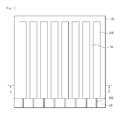
- FIG. 1 is a plan view showing a touch window according to an embodiment.
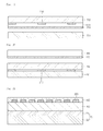
- FIGS. 2 and 3 are sectional views taken along line A-A' of FIG. 1 .
- a touch window includes a substrate 100 having an active area AA, in which a position of an input device (e.g., finger) is detected, and an unactive area UA provided at a peripheral portion of the active area AA.
- an input device e.g., finger
- a sensing electrode 200 may be formed in the active area AA such that the input device may be sensed.
- Wires 300 electrically connecting the sensing electrodes 200 to each other may be formed in the unactive area UA.
- an external circuit connected to the wires 300 may be placed in the unactive area UA.
- the difference in capacitance is made on a touched portion by the input device, and the touched portion representing the difference in capacitance may be detected as a touch point.
- the substrate 100 may be formed of various materials capable of supporting the sensing electrode 200, the wire 300 and a circuit substrate which are formed on the substrate 100.
- the substrate 100 may include a glass substrate, a plastic substrate including polyethylene terephthalate (PET) film, or a sapphire substrate.
- PET polyethylene terephthalate
- the sapphire has superior electric characteristics, such as permittivity, so that a touch response speed may be greatly increased and a space touch such as hovering may be easily implemented.
- the sapphire has a high surface hardness, the sapphire is applicable to a cover substrate.
- the hovering signifies a technique for recognizing a coordinate even in a position spaced apart from a display by a short distance.
- the substrate 100 may be bent to have a partial curved surface. That is, the substrate 100 may be bent to have a partial flat surface and a partial curved surface. In detail, an end of the substrate 100 may be bent to have a curved surface or may be bent or flexed to have a surface including a random curvature.
- the outer dummy layer is formed in the unactive area UA of the substrate 100.
- the outer dummy layer may be coated with a material having a predetermined color so that the wires 300 and a printed circuit board connecting the wires 300 to external circuits cannot be viewed from the outside.
- the outer dummy layer may have a color suitable for a desired outer appearance thereof.
- the outer dummy layer includes black pigments to represent black.
- a desired logo may be formed in the outer dummy layer through various schemes.
- the outer dummy layer may be formed through deposition, print, and wet coating schemes.
- the sensing electrode 200 may be formed on the substrate 100.
- the sensing electrode 200 may detect whether the input device such as a finger is touched thereto or not.
- FIG. 1 shows the sensing electrode 200 extending on the substrate 100 in one direction, but the embodiment is not limited thereto. Accordingly, the sensing electrode 200 may extend in another direction crossing the one direction.
- the sensing electrode 200 may include two types of sensing electrodes having shapes extending in the directions.
- the sensing electrode 200 may include a transparent conductive material.
- the sensing electrode 200 may include metal oxide such as indium tin oxide, indium zinc oxide, copper oxide, tin oxide, zinc oxide or titanium oxide. The materials are very useful for visibility without interrupting transmission of light.
- a protective layer 400 is provided on the sensing electrode 200.
- the protective layer 400 may make direct contact with the sensing electrode 200. That is, the protective layer 400 may make direct contact with a top surface of the sensing electrode 200.
- the protective layer 400 may protect the sensing electrode 200.
- the protective layer 400 may protect the sensing electrode 200 from a physical shock. That is, the protective layer 400 may reinforce the sensing electrode 200 so that the reliability may be improved.
- the protective layer 400 is index-matched with the sensing electrode 200 by adjusting the refractive index, so that the optical property and visibility may be improved.
- the protective layer 400 may include various polymer materials.
- the protective layer 400 may include polyurethane, acrylate, methacrylate, epoxy, polycarbonate, polyethylene or polystyrene.
- the protective layer 400 may have a thickness T in the range of 1 ⁇ m to 20 ⁇ m.
- the thickness T of the protective layer 400 is 1 ⁇ m or more, the sensing electrode 200 may be physically reinforced.
- the thickness T of the protective layer 400 is 20 ⁇ m or less, the thickness of the touch window may be prevented from being increased.
- the thickness of the protective layer 400 may be in the range of 2 ⁇ m to 15 ⁇ m. More preferably, the thickness of the protective layer 400 may be in the range of 4 ⁇ m to 10 ⁇ m.
- the wire 300 is formed in the unactive area UA.
- An electrical signal may be applied to the sensing electrode 200 through the wire 300.
- the wire 300 is formed in the unactive area UA, so that the wire 300 may not be viewed.
- a circuit substrate connected to the wire 300 may be further provided.
- Various types of printed circuit boards may be applied as the circuit substrate.
- a flexible printed circuit board (FPCB) may be applied as the circuit substrate.
- FIGS. 4 to 13 a touch window according to another embodiment will be described with reference to FIGS. 4 to 13 .
- the parts similar or identical to those of the previously described embodiment will be omitted for the purpose of clear and brief description.
- the protective layer 400 includes a first protective layer 401 and a second protective layer 402.
- the first protective layer 401 is provided on a top surface of the sensing electrode 200.
- the second protective layer 402 is provided on a bottom surface of the sensing electrode 200. That is, the top and bottom surfaces of the sensing electrode 200 may be protected through the first and second protective layers 401 and 402. Thus, the strength enhancement of the sensing electrode 200 may be maximized.
- the sensing electrode 200 may include a conductive pattern.
- the sensing electrode 200 is arranged in a mesh shape.
- the sensing electrode 200 may include a mesh opening OA and a mesh line LA.
- a line width of the mesh line LA may be in the range of 0.1 ⁇ m to 10 ⁇ m.
- a mesh line LA of 0.1 ⁇ m or less may not be formed due to the characteristics of the manufacturing process. If the line width is 10 ⁇ m or less, the pattern of the sensing electrode 200 may not be viewed.
- the line width of the mesh line LA may be in the range of 0.5 ⁇ m to 7 ⁇ m. More preferably, the line width of the mesh line LA may be in the range of 1 ⁇ m to 3.5 ⁇ m.
- the mesh opening OA may have a rectangular shape, but the embodiment is not limited thereto.
- the mesh opening OA may have various shapes such as a polygonal shape including a diamond shape, a pentagonal shape or a hexagonal shape, or a circular shape.
- the mesh opening OA may be formed in a regular or random shape.
- the pattern of the sensing electrode 200 may not be viewed in the active area AA. In other words, even when the sensing electrode 200 is formed of metal, the pattern may not be viewed. In addition, even when the sensing electrode 200 is applied to a large-size touch window, the resistance of the touch window may be reduced.
- the sensing electrode 200 may include a first sub-pattern 110, a second sub-pattern 120 and an electrode layer 210.
- the first sub-pattern 110 is disposed on a resin layer 150.
- the first sub-pattern 110 is disposed on the mesh line LA.
- the first sub-pattern 110 is disposed in a mesh shape.
- the first sub-pattern 110 may be embossed.
- the sub-pattern 120 is disposed to be adjacent to the first sub-pattern 120.
- the second sub-pattern 120 is disposed on the resin layer 150.
- the second sub-pattern 120 is disposed in the mesh opening OA.
- the second sub-pattern 120 may be interposed between the first sub-patterns 110.
- the second sub-pattern 120 may be embossed.
- the first and second sub-patterns 110 and 120 may include resin or polymer.
- the first and second sub-patterns 110 and 120 may include resin or polymer.
- the first and second sub-patterns 110 and 120 may be formed through an imprinting process. That is, the first and second sub-patterns 110 and 120 may be formed on the resin layer 150 through a mold on which a desired pattern is formed.
- the electrode layer 210 is disposed on the first sub-pattern 110. Thus, the electrode layer 210 is disposed on the mesh line LA in the mesh shape.
- the sensing electrode 200 may include a metallic material having excellent electric conductivity.
- the sensing electrode 200 may include at least one of Cu, Au, Ag, Al, Ti, Ni and the alloy thereof. Thus, electrical characteristics of the touch window to which the sensing electrode 200 is applied may be improved.
- the protective layer 400 may be disposed on the electrode layer 210.
- the protective layer 400 may be disposed to surround the top and side surfaces of the electrode layer 210. As shown in FIG. 6 , the protective layer 400 may be provided only on the electrode layer 210. Thus, the protective layer 400 may be disposed in the mesh shape.
- the resin layer 150 may be disposed on the substrate 100 and the resin layer 150 may include an intaglio portion 150a.
- the electrode layer 210 may be disposed in the intaglio portions 150a. That is, the sensing electrode 200 may be formed by filling the intaglio portions 150a with an electrode material 270. Therefore, the number, time and cost of processes may be reduced as compared with the deposition and photograph processes according to the related art.
- the sensing electrode 200 having a conductive pattern may be formed by etching the metallic material on the substrate 100. For example, after copper (Cu) is deposited on the substrate, metal etching may be performed to form the sensing electrode 200.
- Cu copper
- the sensing electrode 200 may include an interconnecting structure 222.
- the interconnecting structure 222 may include a fine structure having a diameter in the range of 10 nm to 200 nm.
- the sensing electrode 200 may include a nanowire.
- the sensing electrode 200 may include a metal nanowire.
- the sensing electrode 200 may include a base material 221 and a nanowire.
- the base material 221 includes a photo sensitive material. Since the base material 221 include the photo sensitive material, the sensing electrode 200 may be formed through exposure and development processes.
- the sensing electrode 200 may include a photo sensitive nanowire film. Since the sensitive electrode 200 includes the photo sensitive nanowire film, a thickness of the sensing electrode 200 may be thinned. That is, even though the sensing electrode 200 includes the nanowire, the entire thickness of the sensing electrode 200 may be thinned.
- the protective layer 400 is disposed on a front surface of the substrate 100, the embodiment is not limited thereto. Thus, the protective layer 400 may be disposed only on the sensing electrode 200.
- the substrate includes first and second active areas 1AA and 2AA.
- a first sensing electrode 201 may be disposed in the first active area 1AA.
- the second active area 2AA may be disposed at a side of the first active area 1AA. As shown in the drawings, the second active area 2AA may be disposed at both sides of the first active area 1AA. Referring to FIG. 13 , the second active area 2AA may be bent from the first active area 1AA. That is, the second active area 2AA may be flexible.
- the second active area 2AA which is bent or flexed from the first active area 1AA, is fixed in state that the second active area 2AA is bent, so that the shape in the bent state may be maintained.
- the second active area 2AA may be modified to be bent or flattened corresponding to the quantity and direction of the force applied thereto.
- the first and second sensing electrode 201 and 202 may include mutually different materials.
- the first and second electrode 201 and 202 may include materials having mutually different properties.
- the first sensing electrode 201 may include a first material.
- the first material may include metal oxide such as indium tin oxide, indium zinc oxide, copper oxide, tin oxide, zinc oxide or titanium oxide.
- the first material is very useful for visibility without interrupting transmission of light. However, the first material may also be easily damaged physically due to bending and flexing of the substrate.
- the second sensing electrode 202 may include a second material different from the first material.
- the second material may include various metallic materials including a nanowire, a carbon nanotube (CNT), grapheme or conductive polymer.
- the second sensing electrode 202 may include at least one of Cu, Au, Ag, Al, Ti, Ni and the alloy thereof.
- the second materials have a flexible property suitable for the flexing or bending of the substrate.
- the first sensing electrode 201 may include the second material and the second sensing electrode 202 may include the first material.
- the protective layer 400 is disposed on the second sensing electrode 202. That is, the protective layer 400 is disposed in the second active area 2AA. That is, the protective layer 400 is disposed only in the second active area 2AA which is bent, so that the second sensing electrode 202 may be bent without any physical damage.
- the protective layer 400 may be interposed between the first and second sensing electrode 201 and 202.
- the protective layer 400 is disposed in a boundary area between the first and second active areas 1AA and 2AA. In other words, since the protective layer 400 is disposed in the boundary area in which the protective layer 400 is bent from the first active area 1AA toward the second active area 2AA, the protective layer 400 may be bent without any physical damage when being bent.
- a touch window which is partially bent may be implemented through the protective layer 400.
- the structural variety of a flexible touch window may be secured.
- the protective layer 400 may be additionally disposed even in the first active area 1AA and of course, may be disposed on the front surface of the substrate 100.
- FIGS. 15 and 16 are views illustrating a touch device to which the touch window is applied according to another embodiment.
- the same description as that in the above-described embodiment will be omitted in order to avoid redundancy.
- the same reference numerals will be used to refer to the same elements.
- a touch device may include a touch window which is formed integrally with a touch panel 700. That is, a substrate supporting at least one sensing electrode may be omitted.
- At least one sensing electrode may be formed on at least one surface of the display panel 700.
- the display panel 700 includes first and second substrates 701 and 702. That is, at least one sensing electrode may be formed on at least one surface of the first or second substrate 701 or 702.
- the display panel 700 may be formed in a structure where the first substrate 701 including a thin film transistor (TFT) and a pixel electrode and the second substrate 702 including color filter layers are combined with each other while interposing a liquid crystal layer therebetween.
- TFT thin film transistor
- the display panel 700 may be a liquid crystal display panel having a COT (color filter on transistor) structure in which the second substrate 702 is combined with the first substrate 701 on which a thin film transistor, a color filter and a black matrix are formed while a liquid crystal layer is interposed between the first and second substrates 701 and 702. That is, the thin film transistor is formed on the first substrate 701, the protective layer is formed on the thin film transistor, and the color filter layer is formed on the protective layer.
- the pixel electrode making contact with the thin film transistor is formed on the first substrate 701.
- the black matrix may be omitted and a common electrode may be formed to serve as the black matrix.
- the display device may further include a backlight unit for providing light at the back of the display panel 700.
- the display panel 700 When the display panel 700 is an organic light emitting device, the display panel 700 includes a self light-emitting device which does not require any additional light source.
- a thin film transistor is formed on the first substrate 701 of the display panel 700, and an organic light-emitting device (OLED) making contact with the thin film transistor is formed.
- the OLED may include an anode, a cathode and an organic light-emitting layer formed between the anode and the cathode.
- the display panel 700 may further include the second substrate 702, which performs the function of an encapsulation substrate for encapsulation, on the OLED.
- At least one sensing electrode may be formed on a top surface of the substrate disposed at an upper portion.
- a configuration of forming the sensing electrode on the top surface of the second substrate 702 is depicted in the drawings, if the sensing electrode is disposed on the first substrate 701, at least one sensing electrode may be formed on the top surface of the first substrate 701.
- the first sensing electrode 210 may be formed on the top surface of the display panel 700.
- the first wire connected to the first sensing electrode 210 may be formed.
- the touch substrate 105, on which the second sensing electrode 220 and the second wire are formed, may be formed on the display panel 700 on which the first sensing electrode 210.
- a first adhesive layer 66 may be formed between the touch substrate 105 and the display panel 700.
- the embodiment is not limited thereto.
- the second sensing electrode 220 may be formed on a rear surface of the touch substrate 105. In this case, the touch substrate 105 may serve as the cover substrate.
- the embodiment is not limited to the drawings and is sufficient if the touch device has a structure in which the first sensing electrode 210 is formed on the top surface of the display panel 700, the touch substrate 105 supporting the second sensing electrode 220 is disposed on the display panel 700, and the touch substrate 105 is combined with the display panel 700.
- the touch substrate 105 may be a polarizing plate. That is, the second electrode 220 may be formed on a top or rear surface of the polarizing plate. Thus, the second sensing electrode and the polarizing plate may be integrally formed.
- a polarizing plate may be further provided without regard to the touch substrate 105.
- the polarizing plate may be disposed below the touch substrate 105.
- the polarizing plate may be interposed between the touch substrate 105 and the display panel 700.
- the polarizing plate may be disposed on the touch substrate 105.
- the polarizing plate may be a linear polarizing plate or an anti-reflection polarizing plate.
- the polarizing plate may be a linear polarizing plate.
- the polarizing plate may be an anti-reflection polarizing plate.
- the first and second sensing electrodes 210 and 220 may be formed on the top surface of the display panel 700.
- the first wire connected to the first sensing electrode 210 and the second wire connected to the second sensing electrode 220 may be formed on the top surface of the display panel 700.
- an insulating layer 600 exposing the second sensing electrode 220 may be formed on the first sensing electrode 210.
- a bridge electrode 230 for connecting the second sensing electrodes 220 to each other may be further formed on the insulating layer 600.
- the embodiment is not limited just to the drawings.
- the first sensing electrode 210 and the first and second wires may be formed on the top surface of the display panel 700, and the insulating layer may be formed on the first sensing electrode 210 and the first wire.
- the second electrode 220 may be formed on the insulating layer, and a connecting part for connecting the second sensing electrode 220 and the second wire to each other may be further included.
- first and second sensing electrodes 210 and 220 and the first and second wires may be formed on the top surface of the display panel 700 in the active area.
- the first and second sensing electrodes 210 and 220 may be spaced apart from and adjacent to each other. That is, the insulating layer and the bridge electrode may be omitted.
- the embodiment is not limited to the drawings, and it is sufficient if the first and second sensing electrodes 210 and 220 are formed on the display panel 70 without any additional substrates supporting the sensing electrodes.
- the cover substrate 400 may be disposed on the display panel 700 while an adhesive layer 68 is interposed between the cover substrate and the display panel 700.
- a polarizing plate may be disposed between the display panel 700 and the cover substrate 400.
- FIGS. 17 to 20 are views illustrating a touch device to which a touch window is applied according to still another embodiment.
- the same description as that in the above-described embodiment will be omitted in order to avoid redundancy.
- the same reference numerals will be used to refer to the same elements.
- a touch device may include a touch window formed integrally with a display panel. That is, a substrate supporting at least one sensing electrode may be omitted. All substrates supporting sensing electrodes may be omitted.
- a sensing electrode which serves as a sensor disposed in an active area to sense a touch, and a wire, to which an electrical signal is applied, may be formed inside the display panel.
- a sensing electrode or at least one wire may be formed inside the display panel.
- the display panel includes first and second substrates 701 and 702.
- at least one of the first and second sensing electrodes 210 and 220 is disposed between the first and second substrates 701 and 702. That is, at least one sensing electrode may be formed on at least one surface of the first or second substrate 701 or 702.
- the first and second sensing electrodes 210 and 220 and the first and second wires may be disposed between the first and second substrates 701 and 702. That is, the first and second sensing electrodes 210 and 220 and the first and second wires may be disposed inside the display panel.
- the first sensing electrode 210 and the first wire may be formed on the top surface of the first substrate 710 of the display panel, and the second sensing electrode 220 and the second wire may be formed on a rear surface of the second substrate 702.
- the first and second sensing electrodes 210 and 220 and the first and second wires may be formed on the top surface of the first substrate 701.
- An insulating layer may be formed between the first and second sensing electrodes 210 and 220.
- the first and second sensing electrodes 210 and 220 may be formed on the rear surface of the second substrate 702.
- An insulating layer 630 may be formed between the first and second sensing electrodes 210 and 220.
- the first sensing electrode 210 and the first wire may be formed between the first and second substrates 701 and 702.
- the second sensing electrode 220 and the second wire may be formed on the touch substrate 106.
- the touch substrate 106 may be disposed on the display panel including the first and second substrates 701 and 702. That is, the first sensing electrode 210 and the first wire may be disposed inside the display panel, and the second sensing electrode 220 and the second wire may be disposed outside the display panel.
- the first sensing electrode 210 and the first wire may be formed on the top surface of the first substrate 701 or the rear surface of the second substrate 702.
- the adhesive layer may be formed between the touch substrate 106 and the display panel.
- the touch substrate 106 may serve as the cover substrate.
- the second sensing electrode 220 may be formed on the top surface of the touch substrate 106, and the cover substrate may be further formed while being interposed between the touch substrate 106 and the adhesive layer.
- the embodiment is not limited to the drawings, and it is sufficient if the embodiment has a structure that the first sensing electrode 210 and the first wire are disposed inside the display panel and the second electrode 220 and the second wire are disposed outside the display panel.
- the touch substrate 106 may be a polarizing plate. That is, the second sensing electrode 220 may be formed on the top or rear surface of the polarizing plate. Thus, the second sensing electrode may be formed integrally with the polarizing plate.
- the polarizing plate may be further provided without regard to the touch substrate 106.
- the polarizing plate may be disposed below the touch substrate 106.
- the polarizing plate may be interposed between the touch substrate 106 and the display panel.
- the polarizing plate may be disposed on the touch substrate 106.
- the sensing electrode When the display panel is a liquid crystal display panel and the sensing electrode is formed on the top surface of the first substrate 701, the sensing electrode may be formed together with a thin film transistor (TFT) and a pixel electrode. In addition, when the sensing electrode is formed on the rear surface of the second substrate 702, a color filter layer may be formed on the sensing electrode or the sensing electrode may be formed on the color filter layer.
- TFT thin film transistor
- the sensing electrode may be formed together with a thin film transistor or an organic light emitting device.
- the touch window 10 may be disposed on a display panel 20 serving as a driver.
- the touch window 10 may be combined with the display panel 20, so that a touch device may be implemented.
- a display region to output an image is formed in the display panel 20.
- a display panel applied to the touch device may generally include an upper substrate 21 and a lower substrate 22.
- a data line, a gate line and a thin-film transistor (TFT) may be formed in the lower substrate 22.
- the upper substrate 21 may be adhesive to the lower substrate 22 such that the elements provided on the lower substrate 22 may be protected.
- the display panel 20 may be formed in various types according to the type of touch device. That is, the touch device according to the embodiment may include a liquid-crystal device (LCD), a field emission display, a plasma display panel (PDP), an organic light-emitting diode (OLED), and an electronic paper display (EPD). Thus, the display panel 20 may be implemented in various types.
- LCD liquid-crystal device
- PDP plasma display panel
- OLED organic light-emitting diode
- EPD electronic paper display
- such a touch device may be a mobile terminal.
- the touch window may include a curved touch window. Therefore, a touch device including it may be a curved display device.
- the touch device may be a touch device of which only an edge may be bent.
- the touch device may include a curved display device and may have an entirely bent shape.
- the touch window may include a flexible touch window.
- the display device including it may be a flexible touch device. Therefore, a user may flex or bend the display device with his hand.
- the touch window may be applied to a vehicle navigation system as well as a mobile terminal.
- vehicle navigation system is depicted in the drawings, the embodiment is not limited thereto.
- the touch window is applied to a dashboard as well as a PND (Personal Navigation Display) so that a CID (Center Information Display) may be implemented.
- the embodiment is not limited to the embodiment. In other words, the display may be used in various electronic products.
- any reference in this specification to "one embodiment,” “an embodiment,” “example embodiment,” etc. means that a particular feature, structure, or characteristic described in connection with the embodiment is included in at least one embodiment of the invention.
- the appearances of such phrases in various places in the specification are not necessarily all referring to the same embodiment.
Landscapes
- Engineering & Computer Science (AREA)
- General Engineering & Computer Science (AREA)
- Theoretical Computer Science (AREA)
- Human Computer Interaction (AREA)
- Physics & Mathematics (AREA)
- General Physics & Mathematics (AREA)
- Position Input By Displaying (AREA)
Abstract
Description
- The disclosure relates to a touch window and a touch device including the same.
- Recently, a touch panel, which performs an input function through the touch of an image displayed on a touch device by an input device such as a stylus pen or a hand, has been applied to various electronic appliances.
- The touch panel may be typically classified into a resistive touch panel and a capacitive touch panel. In the resistive touch panel, the position of the touch point is detected by detecting the variation of resistance according to the connection between electrodes when pressure is applied to an input device. In the capacitive touch panel, the position of the touch point is detected by detecting the variation in capacitance when a finger of the user is touched on the capacitive touch panel between electrodes. When taking into consideration the convenience of a fabrication scheme and a sensing power, the capacitive touch panel has been spotlighted in a smaller model touch panel recently.
- Meanwhile, the demand for a flexible touch panel has been increased recently. That is, if the touch panel is flexible or bendable, the experience of a user will extend. However, indium tin oxide (ITO), which is the most widely used material for the transparent electrode of the touch panel, is easy to be physically damaged when the substrate is flexed and bent, so that the electrode property is deteriorated. Therefore, the indium tin oxide (ITO) is not suitable for a flexible device. Meanwhile, when a flexible material instead of ITO is used for the transparent electrode, the visibility of the flexible material is poorer than that of ITO due to light reflection.
- The embodiment is to provide a touch window of which reliability is improved, and a touch device including the same.
- A touch window according to an embodiment includes a substrate; a sensing electrode disposed on the substrate to sense a position; and a protective layer on the sensing electrode.
- A touch device according to an embodiment includes a touch window; and a driving part on the touch window, wherein the touch window includes: a substrate; a sensing electrode disposed on the substrate to sense a position; and a protective layer on the sensing electrode.
- According to the touch window of the embodiment, when the substrate is bent or flexed, the protective layer may protect the sensing electrode from a physical shock. That is, the protective layer may reinforce the sensing electrode so that the reliability may be improved.
- In addition, the protective layer is index-matched with the sensing electrode by adjusting the refractive index to the sensing electrode, so that the optical property and visibility may be improved.
-
-
FIG. 1 is a plan view showing a touch window according to an embodiment. -
FIGS. 2 and 3 are sectional views taken along line A-A' ofFIG. 1 . -
FIG. 4 is a sectional view showing a touch window according to another embodiment. -
FIG. 5 is a plan view showing a touch window according to another embodiment. -
FIG. 6 is a sectional view taken along line B-B' ofFIG. 5 . -
FIGS. 7 to 10 are sectional views showing a touch window according to another embodiment. -
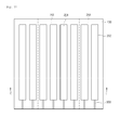
FIG. 11 is a plan view showing a touch window according to another embodiment. -
FIGS. 12 to 14 are sectional views taken along line C-C' ofFIG. 11 . -
FIGS. 15 and 16 are views illustrating a touch device according to another embodiment. -
FIGS. 17 to 20 are views illustrating a touch device according to another embodiment. -
FIG. 21 is a sectional view showing a touch device in which a touch window is disposed on a driving part according to an embodiment. -
FIGS. 22 to 25 are perspective views showing a touch device according to another embodiment. - In the following description of the embodiments, it will be understood that, when a layer (or film), a region, a pattern, or a structure is referred to as being "on" or "under" another substrate, another layer (or film), another region, another pad, or another pattern, it can be "directly" or "indirectly" on the other substrate, layer (or film), region, pad, or pattern, or one or more intervening layers may also be present. Such a position of the layer has been described with reference to the drawings.
- The thickness and size of each layer shown in the drawings may be exaggerated, omitted or schematically drawn for the purpose of convenience or clarity. In addition, the size of elements does not utterly reflect an actual size.
- Hereinafter, the embodiment will be described with reference to accompanying drawings.
- First, a touch window according to an embodiment will be described in detail with reference to
FIGS. 1 to 3 .FIG. 1 is a plan view showing a touch window according to an embodiment.FIGS. 2 and 3 are sectional views taken along line A-A' ofFIG. 1 . - Referring to
FIG. 1 , a touch window according to the embodiment includes asubstrate 100 having an active area AA, in which a position of an input device (e.g., finger) is detected, and an unactive area UA provided at a peripheral portion of the active area AA. - In this case, a
sensing electrode 200 may be formed in the active area AA such that the input device may be sensed.Wires 300 electrically connecting thesensing electrodes 200 to each other may be formed in the unactive area UA. In addition, an external circuit connected to thewires 300 may be placed in the unactive area UA. - When an input device such as a finger is touched onto such a touch window, the difference in capacitance is made on a touched portion by the input device, and the touched portion representing the difference in capacitance may be detected as a touch point.
- Such a touch window will be described in more detail as follows.
- The
substrate 100 may be formed of various materials capable of supporting thesensing electrode 200, thewire 300 and a circuit substrate which are formed on thesubstrate 100. Thesubstrate 100 may include a glass substrate, a plastic substrate including polyethylene terephthalate (PET) film, or a sapphire substrate. - The sapphire has superior electric characteristics, such as permittivity, so that a touch response speed may be greatly increased and a space touch such as hovering may be easily implemented. In addition since the sapphire has a high surface hardness, the sapphire is applicable to a cover substrate. The hovering signifies a technique for recognizing a coordinate even in a position spaced apart from a display by a short distance. Further, the
substrate 100 may be bent to have a partial curved surface. That is, thesubstrate 100 may be bent to have a partial flat surface and a partial curved surface. In detail, an end of thesubstrate 100 may be bent to have a curved surface or may be bent or flexed to have a surface including a random curvature. - The outer dummy layer is formed in the unactive area UA of the
substrate 100. The outer dummy layer may be coated with a material having a predetermined color so that thewires 300 and a printed circuit board connecting thewires 300 to external circuits cannot be viewed from the outside. The outer dummy layer may have a color suitable for a desired outer appearance thereof. For example, the outer dummy layer includes black pigments to represent black. In addition, a desired logo may be formed in the outer dummy layer through various schemes. The outer dummy layer may be formed through deposition, print, and wet coating schemes. - The
sensing electrode 200 may be formed on thesubstrate 100. Thesensing electrode 200 may detect whether the input device such as a finger is touched thereto or not.FIG. 1 shows thesensing electrode 200 extending on thesubstrate 100 in one direction, but the embodiment is not limited thereto. Accordingly, thesensing electrode 200 may extend in another direction crossing the one direction. In addition, thesensing electrode 200 may include two types of sensing electrodes having shapes extending in the directions. - The
sensing electrode 200 may include a transparent conductive material. For example, thesensing electrode 200 may include metal oxide such as indium tin oxide, indium zinc oxide, copper oxide, tin oxide, zinc oxide or titanium oxide. The materials are very useful for visibility without interrupting transmission of light. - A
protective layer 400 is provided on thesensing electrode 200. Theprotective layer 400 may make direct contact with thesensing electrode 200. That is, theprotective layer 400 may make direct contact with a top surface of thesensing electrode 200. Theprotective layer 400 may protect thesensing electrode 200. In detail, as shown inFIG. 3 , when the substrate is bent or flexed, theprotective layer 400 may protect thesensing electrode 200 from a physical shock. That is, theprotective layer 400 may reinforce thesensing electrode 200 so that the reliability may be improved. - In addition, the
protective layer 400 is index-matched with thesensing electrode 200 by adjusting the refractive index, so that the optical property and visibility may be improved. - The
protective layer 400 may include various polymer materials. Theprotective layer 400 may include polyurethane, acrylate, methacrylate, epoxy, polycarbonate, polyethylene or polystyrene. - The
protective layer 400 may have a thickness T in the range of 1 µm to 20 µm. When the thickness T of theprotective layer 400 is 1 µm or more, thesensing electrode 200 may be physically reinforced. When the thickness T of theprotective layer 400 is 20 µm or less, the thickness of the touch window may be prevented from being increased. Preferably, the thickness of theprotective layer 400 may be in the range of 2 µm to 15 µm. More preferably, the thickness of theprotective layer 400 may be in the range of 4 µm to 10 µm. - Then, the
wire 300 is formed in the unactive area UA. An electrical signal may be applied to thesensing electrode 200 through thewire 300. Thewire 300 is formed in the unactive area UA, so that thewire 300 may not be viewed. - Meanwhile, although not shown in the drawings, a circuit substrate connected to the
wire 300 may be further provided. Various types of printed circuit boards may be applied as the circuit substrate. For example, a flexible printed circuit board (FPCB) may be applied as the circuit substrate. - Hereinafter, a touch window according to another embodiment will be described with reference to
FIGS. 4 to 13 . In the following description about the touch window according to another embodiment, the parts similar or identical to those of the previously described embodiment will be omitted for the purpose of clear and brief description. - First, referring to
FIG. 4 , theprotective layer 400 includes a first protective layer 401 and a secondprotective layer 402. The first protective layer 401 is provided on a top surface of thesensing electrode 200. The secondprotective layer 402 is provided on a bottom surface of thesensing electrode 200. That is, the top and bottom surfaces of thesensing electrode 200 may be protected through the first and secondprotective layers 401 and 402. Thus, the strength enhancement of thesensing electrode 200 may be maximized. - Then, referring to
FIGS. 5 and6 , thesensing electrode 200 may include a conductive pattern. For example, thesensing electrode 200 is arranged in a mesh shape. - In detail, the
sensing electrode 200 may include a mesh opening OA and a mesh line LA. In this case, a line width of the mesh line LA may be in the range of 0.1 µm to 10 µm. A mesh line LA of 0.1 µm or less may not be formed due to the characteristics of the manufacturing process. If the line width is 10 µm or less, the pattern of thesensing electrode 200 may not be viewed. Preferably, the line width of the mesh line LA may be in the range of 0.5 µm to 7 µm. More preferably, the line width of the mesh line LA may be in the range of 1 µm to 3.5 µm. - Meanwhile, as shown in
FIG. 5 , the mesh opening OA may have a rectangular shape, but the embodiment is not limited thereto. The mesh opening OA may have various shapes such as a polygonal shape including a diamond shape, a pentagonal shape or a hexagonal shape, or a circular shape. In addition, the mesh opening OA may be formed in a regular or random shape. - As the
sensing electrode 200 has a mesh shape, the pattern of thesensing electrode 200 may not be viewed in the active area AA. In other words, even when thesensing electrode 200 is formed of metal, the pattern may not be viewed. In addition, even when thesensing electrode 200 is applied to a large-size touch window, the resistance of the touch window may be reduced. - Referring to
FIG. 6 , thesensing electrode 200 may include afirst sub-pattern 110, asecond sub-pattern 120 and anelectrode layer 210. - The
first sub-pattern 110 is disposed on aresin layer 150. Thefirst sub-pattern 110 is disposed on the mesh line LA. Thus, thefirst sub-pattern 110 is disposed in a mesh shape. Thefirst sub-pattern 110 may be embossed. - Meanwhile, the sub-pattern 120 is disposed to be adjacent to the
first sub-pattern 120. Thesecond sub-pattern 120 is disposed on theresin layer 150. Thesecond sub-pattern 120 is disposed in the mesh opening OA. Thus, thesecond sub-pattern 120 may be interposed between thefirst sub-patterns 110. Thesecond sub-pattern 120 may be embossed. - The first and second sub-patterns 110 and 120 may include resin or polymer. The first and second sub-patterns 110 and 120 may include resin or polymer. The first and second sub-patterns 110 and 120 may be formed through an imprinting process. That is, the first and second sub-patterns 110 and 120 may be formed on the
resin layer 150 through a mold on which a desired pattern is formed. - The
electrode layer 210 is disposed on thefirst sub-pattern 110. Thus, theelectrode layer 210 is disposed on the mesh line LA in the mesh shape. - The
sensing electrode 200 may include a metallic material having excellent electric conductivity. For example, thesensing electrode 200 may include at least one of Cu, Au, Ag, Al, Ti, Ni and the alloy thereof. Thus, electrical characteristics of the touch window to which thesensing electrode 200 is applied may be improved. - The
protective layer 400 may be disposed on theelectrode layer 210. Theprotective layer 400 may be disposed to surround the top and side surfaces of theelectrode layer 210. As shown inFIG. 6 , theprotective layer 400 may be provided only on theelectrode layer 210. Thus, theprotective layer 400 may be disposed in the mesh shape. - Meanwhile, referring to
FIG. 7 , theresin layer 150 may be disposed on thesubstrate 100 and theresin layer 150 may include anintaglio portion 150a. In this case, theelectrode layer 210 may be disposed in theintaglio portions 150a. That is, thesensing electrode 200 may be formed by filling theintaglio portions 150a with anelectrode material 270. Therefore, the number, time and cost of processes may be reduced as compared with the deposition and photograph processes according to the related art. - Referring to
FIG. 8 , thesensing electrode 200 having a conductive pattern may be formed by etching the metallic material on thesubstrate 100. For example, after copper (Cu) is deposited on the substrate, metal etching may be performed to form thesensing electrode 200. - Referring to
FIG. 9 , thesensing electrode 200 may include an interconnectingstructure 222. The interconnectingstructure 222 may include a fine structure having a diameter in the range of 10 nm to 200 nm. For example, thesensing electrode 200 may include a nanowire. Thesensing electrode 200 may include a metal nanowire. - Referring to
FIG. 10 , thesensing electrode 200 may include abase material 221 and a nanowire. Thebase material 221 includes a photo sensitive material. Since thebase material 221 include the photo sensitive material, thesensing electrode 200 may be formed through exposure and development processes. - The
sensing electrode 200 may include a photo sensitive nanowire film. Since thesensitive electrode 200 includes the photo sensitive nanowire film, a thickness of thesensing electrode 200 may be thinned. That is, even though thesensing electrode 200 includes the nanowire, the entire thickness of thesensing electrode 200 may be thinned. - Meanwhile, although it is shown that the
protective layer 400 is disposed on a front surface of thesubstrate 100, the embodiment is not limited thereto. Thus, theprotective layer 400 may be disposed only on thesensing electrode 200. - Then, referring to
FIGS. 11 to 14 , the substrate includes first and second active areas 1AA and 2AA. - A
first sensing electrode 201 may be disposed in the first active area 1AA. - The second active area 2AA may be disposed at a side of the first active area 1AA. As shown in the drawings, the second active area 2AA may be disposed at both sides of the first active area 1AA. Referring to
FIG. 13 , the second active area 2AA may be bent from the first active area 1AA. That is, the second active area 2AA may be flexible. - The second active area 2AA, which is bent or flexed from the first active area 1AA, is fixed in state that the second active area 2AA is bent, so that the shape in the bent state may be maintained. In addition, when physical force is applied in the direction opposite to the bending direction in a state that the bent state is maintained, the second active area 2AA may be modified to be bent or flattened corresponding to the quantity and direction of the force applied thereto.
- The first and
second sensing electrode second electrode - For example, the
first sensing electrode 201 may include a first material. The first material may include metal oxide such as indium tin oxide, indium zinc oxide, copper oxide, tin oxide, zinc oxide or titanium oxide. The first material is very useful for visibility without interrupting transmission of light. However, the first material may also be easily damaged physically due to bending and flexing of the substrate. - The
second sensing electrode 202 may include a second material different from the first material. For example, the second material may include various metallic materials including a nanowire, a carbon nanotube (CNT), grapheme or conductive polymer. In addition, thesecond sensing electrode 202 may include at least one of Cu, Au, Ag, Al, Ti, Ni and the alloy thereof. The second materials have a flexible property suitable for the flexing or bending of the substrate. - Meanwhile, to the contrary, the
first sensing electrode 201 may include the second material and thesecond sensing electrode 202 may include the first material. - In this case, the
protective layer 400 is disposed on thesecond sensing electrode 202. That is, theprotective layer 400 is disposed in the second active area 2AA. That is, theprotective layer 400 is disposed only in the second active area 2AA which is bent, so that thesecond sensing electrode 202 may be bent without any physical damage. - In addition, the
protective layer 400 may be interposed between the first andsecond sensing electrode protective layer 400 is disposed in a boundary area between the first and second active areas 1AA and 2AA. In other words, since theprotective layer 400 is disposed in the boundary area in which theprotective layer 400 is bent from the first active area 1AA toward the second active area 2AA, theprotective layer 400 may be bent without any physical damage when being bent. - . That is, a touch window which is partially bent may be implemented through the
protective layer 400. Thus, the structural variety of a flexible touch window may be secured. - Meanwhile, the
protective layer 400 may be additionally disposed even in the first active area 1AA and of course, may be disposed on the front surface of thesubstrate 100. - A touch device to which the touch window is applied according to another embodiment of the present invention will be described with reference to
FIGS. 15 and 16. FIGS. 15 and 16 are views illustrating a touch device to which the touch window is applied according to another embodiment. The same description as that in the above-described embodiment will be omitted in order to avoid redundancy. The same reference numerals will be used to refer to the same elements. - Referring to
FIGS. 15 and 16 , a touch device according to another embodiment may include a touch window which is formed integrally with atouch panel 700. That is, a substrate supporting at least one sensing electrode may be omitted. - In detail, at least one sensing electrode may be formed on at least one surface of the
display panel 700. Thedisplay panel 700 includes first andsecond substrates second substrate - When the
display panel 700 is a liquid crystal display panel, thedisplay panel 700 may be formed in a structure where thefirst substrate 701 including a thin film transistor (TFT) and a pixel electrode and thesecond substrate 702 including color filter layers are combined with each other while interposing a liquid crystal layer therebetween. - In addition, the
display panel 700 may be a liquid crystal display panel having a COT (color filter on transistor) structure in which thesecond substrate 702 is combined with thefirst substrate 701 on which a thin film transistor, a color filter and a black matrix are formed while a liquid crystal layer is interposed between the first andsecond substrates first substrate 701, the protective layer is formed on the thin film transistor, and the color filter layer is formed on the protective layer. In addition, the pixel electrode making contact with the thin film transistor is formed on thefirst substrate 701. In this case, in order to improve an aperture rate and simplify a mask process, the black matrix may be omitted and a common electrode may be formed to serve as the black matrix. - In addition, when the
display panel 700 is a liquid crystal panel, the display device may further include a backlight unit for providing light at the back of thedisplay panel 700. - When the
display panel 700 is an organic light emitting device, thedisplay panel 700 includes a self light-emitting device which does not require any additional light source. A thin film transistor is formed on thefirst substrate 701 of thedisplay panel 700, and an organic light-emitting device (OLED) making contact with the thin film transistor is formed. The OLED may include an anode, a cathode and an organic light-emitting layer formed between the anode and the cathode. In addition, thedisplay panel 700 may further include thesecond substrate 702, which performs the function of an encapsulation substrate for encapsulation, on the OLED. - In this case, at least one sensing electrode may be formed on a top surface of the substrate disposed at an upper portion. Although a configuration of forming the sensing electrode on the top surface of the
second substrate 702 is depicted in the drawings, if the sensing electrode is disposed on thefirst substrate 701, at least one sensing electrode may be formed on the top surface of thefirst substrate 701. - Referring to
FIG. 15 , thefirst sensing electrode 210 may be formed on the top surface of thedisplay panel 700. In addition, the first wire connected to thefirst sensing electrode 210 may be formed. Thetouch substrate 105, on which thesecond sensing electrode 220 and the second wire are formed, may be formed on thedisplay panel 700 on which thefirst sensing electrode 210. A firstadhesive layer 66 may be formed between thetouch substrate 105 and thedisplay panel 700. - Although the
second sensing electrode 220 formed on the top surface of thetouch substrate 105 and thecover substrate 400 disposed on the touch substrate while a secondadhesive layer 67 is interposed between thesecond sensing electrode 220 and thecover substrate 400 are depicted in the drawings, the embodiment is not limited thereto. Thesecond sensing electrode 220 may be formed on a rear surface of thetouch substrate 105. In this case, thetouch substrate 105 may serve as the cover substrate. - That is, the embodiment is not limited to the drawings and is sufficient if the touch device has a structure in which the
first sensing electrode 210 is formed on the top surface of thedisplay panel 700, thetouch substrate 105 supporting thesecond sensing electrode 220 is disposed on thedisplay panel 700, and thetouch substrate 105 is combined with thedisplay panel 700. - In addition, the
touch substrate 105 may be a polarizing plate. That is, thesecond electrode 220 may be formed on a top or rear surface of the polarizing plate. Thus, the second sensing electrode and the polarizing plate may be integrally formed. - In addition, a polarizing plate may be further provided without regard to the
touch substrate 105. In this case, the polarizing plate may be disposed below thetouch substrate 105. For example, the polarizing plate may be interposed between thetouch substrate 105 and thedisplay panel 700. In addition, the polarizing plate may be disposed on thetouch substrate 105. - The polarizing plate may be a linear polarizing plate or an anti-reflection polarizing plate. For example, when the
display panel 700 is a liquid crystal display panel, the polarizing plate may be a linear polarizing plate. In addition, when thedisplay panel 700 is an organic electroluminescent display panel, the polarizing plate may be an anti-reflection polarizing plate. - Referring to
FIG. 16 , the first andsecond sensing electrodes display panel 700. In addition, the first wire connected to thefirst sensing electrode 210 and the second wire connected to thesecond sensing electrode 220 may be formed on the top surface of thedisplay panel 700. - In addition, an insulating
layer 600 exposing thesecond sensing electrode 220 may be formed on thefirst sensing electrode 210. Abridge electrode 230 for connecting thesecond sensing electrodes 220 to each other may be further formed on the insulatinglayer 600. - The embodiment is not limited just to the drawings. The
first sensing electrode 210 and the first and second wires may be formed on the top surface of thedisplay panel 700, and the insulating layer may be formed on thefirst sensing electrode 210 and the first wire. Thesecond electrode 220 may be formed on the insulating layer, and a connecting part for connecting thesecond sensing electrode 220 and the second wire to each other may be further included. - In addition, the first and
second sensing electrodes display panel 700 in the active area. The first andsecond sensing electrodes - That is, the embodiment is not limited to the drawings, and it is sufficient if the first and
second sensing electrodes - The
cover substrate 400 may be disposed on thedisplay panel 700 while anadhesive layer 68 is interposed between the cover substrate and thedisplay panel 700. In this case, a polarizing plate may be disposed between thedisplay panel 700 and thecover substrate 400. - Next, a touch device according to still another embodiment will be described with reference to
FIGS. 17 to 20. FIGS. 17 to 20 are views illustrating a touch device to which a touch window is applied according to still another embodiment. The same description as that in the above-described embodiment will be omitted in order to avoid redundancy. The same reference numerals will be used to refer to the same elements. - Referring to
FIGS. 17 to 20 , a touch device according to still another embodiment may include a touch window formed integrally with a display panel. That is, a substrate supporting at least one sensing electrode may be omitted. All substrates supporting sensing electrodes may be omitted. - A sensing electrode, which serves as a sensor disposed in an active area to sense a touch, and a wire, to which an electrical signal is applied, may be formed inside the display panel. In detail, at least one sensing electrode or at least one wire may be formed inside the display panel.
- The display panel includes first and
second substrates second sensing electrodes second substrates second substrate - Referring to
FIGS. 17 and20 , the first andsecond sensing electrodes second substrates second sensing electrodes - Referring to
FIG. 17 , thefirst sensing electrode 210 and the first wire may be formed on the top surface of the first substrate 710 of the display panel, and thesecond sensing electrode 220 and the second wire may be formed on a rear surface of thesecond substrate 702. Referring toFIG. 18 , the first andsecond sensing electrodes first substrate 701. An insulating layer may be formed between the first andsecond sensing electrodes FIG. 19 , the first andsecond sensing electrodes second substrate 702. An insulatinglayer 630 may be formed between the first andsecond sensing electrodes - Referring to
FIG. 20 , thefirst sensing electrode 210 and the first wire may be formed between the first andsecond substrates second sensing electrode 220 and the second wire may be formed on thetouch substrate 106. Thetouch substrate 106 may be disposed on the display panel including the first andsecond substrates first sensing electrode 210 and the first wire may be disposed inside the display panel, and thesecond sensing electrode 220 and the second wire may be disposed outside the display panel. - The
first sensing electrode 210 and the first wire may be formed on the top surface of thefirst substrate 701 or the rear surface of thesecond substrate 702. In addition, the adhesive layer may be formed between thetouch substrate 106 and the display panel. In this case, thetouch substrate 106 may serve as the cover substrate. - Although the configuration of forming the
second sensing electrode 220 on the rear surface of thetouch substrate 106 is depicted in the drawings, but the embodiment is not limited thereto. Thesecond sensing electrode 220 may be formed on the top surface of thetouch substrate 106, and the cover substrate may be further formed while being interposed between thetouch substrate 106 and the adhesive layer. - That is, the embodiment is not limited to the drawings, and it is sufficient if the embodiment has a structure that the
first sensing electrode 210 and the first wire are disposed inside the display panel and thesecond electrode 220 and the second wire are disposed outside the display panel. - In addition, the
touch substrate 106 may be a polarizing plate. That is, thesecond sensing electrode 220 may be formed on the top or rear surface of the polarizing plate. Thus, the second sensing electrode may be formed integrally with the polarizing plate. - In addition, the polarizing plate may be further provided without regard to the
touch substrate 106. In this case, the polarizing plate may be disposed below thetouch substrate 106. For example, the polarizing plate may be interposed between thetouch substrate 106 and the display panel. In addition, the polarizing plate may be disposed on thetouch substrate 106. - When the display panel is a liquid crystal display panel and the sensing electrode is formed on the top surface of the
first substrate 701, the sensing electrode may be formed together with a thin film transistor (TFT) and a pixel electrode. In addition, when the sensing electrode is formed on the rear surface of thesecond substrate 702, a color filter layer may be formed on the sensing electrode or the sensing electrode may be formed on the color filter layer. When the display panel is an organic light emitting device and the sensing electrode is formed on the top surface of thefirst substrate 701, the sensing electrode may be formed together with a thin film transistor or an organic light emitting device. - Meanwhile, referring to
FIG. 15 , the touch window 10 may be disposed on adisplay panel 20 serving as a driver. The touch window 10 may be combined with thedisplay panel 20, so that a touch device may be implemented. - A display region to output an image is formed in the
display panel 20. A display panel applied to the touch device may generally include anupper substrate 21 and alower substrate 22. A data line, a gate line and a thin-film transistor (TFT) may be formed in thelower substrate 22. Theupper substrate 21 may be adhesive to thelower substrate 22 such that the elements provided on thelower substrate 22 may be protected. - The
display panel 20 may be formed in various types according to the type of touch device. That is, the touch device according to the embodiment may include a liquid-crystal device (LCD), a field emission display, a plasma display panel (PDP), an organic light-emitting diode (OLED), and an electronic paper display (EPD). Thus, thedisplay panel 20 may be implemented in various types. - As shown in
FIG. 16 , such a touch device may be a mobile terminal. Specifically, the touch window may include a curved touch window. Therefore, a touch device including it may be a curved display device. Specifically, the touch device may be a touch device of which only an edge may be bent. - Meanwhile, referring to
FIG. 17 , the touch device may include a curved display device and may have an entirely bent shape. - Meanwhile, referring to
FIG. 18 , the touch window may include a flexible touch window. Thus, the display device including it may be a flexible touch device. Therefore, a user may flex or bend the display device with his hand. - Meanwhile, referring to
FIG. 19 , the touch window may be applied to a vehicle navigation system as well as a mobile terminal. Although the vehicle navigation system is depicted in the drawings, the embodiment is not limited thereto. Accordingly, the touch window is applied to a dashboard as well as a PND (Personal Navigation Display) so that a CID (Center Information Display) may be implemented. However, the embodiment is not limited to the embodiment. In other words, the display may be used in various electronic products. - Any reference in this specification to "one embodiment," "an embodiment," "example embodiment," etc., means that a particular feature, structure, or characteristic described in connection with the embodiment is included in at least one embodiment of the invention. The appearances of such phrases in various places in the specification are not necessarily all referring to the same embodiment. Further, when a particular feature, structure, or characteristic is described in connection with any embodiment, it is submitted that it is within the purview of one skilled in the art to effect such feature, structure, or characteristic in connection with other ones of the embodiments.
- Although embodiments have been described with reference to a number of illustrative embodiments thereof, it should be understood that numerous other modifications and embodiments can be devised by those skilled in the art that will fall within the spirit and scope of the principles of this disclosure. More particularly, various variations and modifications are possible in the component parts and/or arrangements of the subject combination arrangement within the scope of the disclosure, the drawings and the appended claims. In addition to variations and modifications in the component parts and/or arrangements, alternative uses will also be apparent to those skilled in the art.
Claims (14)
- A touch window comprising:a substrate (100) including a first active area (1AA) and a second active area (2AA) flexible from the first active area (1AA);a sensing electrode (200) disposed on the substrate (100) to sense a position; anda protective layer (400) on the sensing electrode (200),wherein the protective layer (400) is disposed in the second active area (2AA).
- The touch window of claim 1, wherein the protective layer (400) makes direct contact with the sensing electrode (200).
- The touch window of claim 1, wherein the protective layer (400) includes a first protective layer (401) on a top surface of the sensing electrode (200) and a second protective layer (402) on a bottom surface of the sensing electrode (200).
- The touch window of any one of claim 1 to 3, wherein the sensing electrode (200) includes a transparent conductive material.
- The touch window any one of claim 1 to 3, wherein the sensing electrode (200) includes a conductive pattern.
- The touch window any one of claim 1 to 4, wherein the sensing electrode (200) includes one selected from the group consisting of a nanowire, a carbon nanotube (CNT), grapheme and a metal.
- The touch window any one of claim 1 to 6, wherein the protective layer (400) includes polymer.
- The touch window any one of claim 1 to 7, wherein the protective layer (400) includes one selected from the group consisting of polyurethane, acrylate, methacrylate, epoxy, polycarbonate, polyethylene and polystyrene.
- The touch window of claim any one of claim 1 to 8, wherein the protective layer (400) has a thickness in a range of 1 µm to 20 µm.
- The touch window any one of claim 1 to 9, wherein the substrate (100) is flexible.
- The touch window any one of claim 1 to 10, wherein the protective layer (400) is further disposed in the first active area (1AA).
- The touch window of claim 11, wherein a first sensing electrode (201) is disposed in the first active area (1AA); and
a second sensing electrode (202) is disposed in the second active area (2AA),
wherein the first and second sensing electrodes (201,202) include mutually different materials. - A touch device comprising:a touch window according to any one of the preceding claims ; anda driving part (20) on the touch window.
- The touch device of claim 13, wherein the touch window includes a curved or flexible touch window.
Applications Claiming Priority (1)
| Application Number | Priority Date | Filing Date | Title |
|---|---|---|---|
| KR1020130107066A KR102119603B1 (en) | 2013-09-06 | 2013-09-06 | Touch window and display with the same |
Publications (3)
| Publication Number | Publication Date |
|---|---|
| EP2846236A2 true EP2846236A2 (en) | 2015-03-11 |
| EP2846236A3 EP2846236A3 (en) | 2015-04-15 |
| EP2846236B1 EP2846236B1 (en) | 2022-12-21 |
Family
ID=51429098
Family Applications (1)
| Application Number | Title | Priority Date | Filing Date |
|---|---|---|---|
| EP14182756.8A Active EP2846236B1 (en) | 2013-09-06 | 2014-08-29 | Touch window and touch device including the same |
Country Status (6)
| Country | Link |
|---|---|
| US (2) | US9791981B2 (en) |
| EP (1) | EP2846236B1 (en) |
| JP (1) | JP6553339B2 (en) |
| KR (1) | KR102119603B1 (en) |
| CN (1) | CN104423708B (en) |
| TW (1) | TWI633477B (en) |
Cited By (1)
| Publication number | Priority date | Publication date | Assignee | Title |
|---|---|---|---|---|
| EP4105769A4 (en) * | 2020-02-12 | 2023-03-29 | BOE Technology Group Co., Ltd. | TOUCH CONTROL DISPLAY SUBSTRATE AND TOUCH CONTROL DISPLAY APPARATUS |
Families Citing this family (48)
| Publication number | Priority date | Publication date | Assignee | Title |
|---|---|---|---|---|
| US10261370B2 (en) | 2011-10-05 | 2019-04-16 | Apple Inc. | Displays with minimized border regions having an apertured TFT layer for signal conductors |
| CN104345952B (en) * | 2013-08-09 | 2017-09-12 | 天津富纳源创科技有限公司 | The preparation method of curved surface touch module |
| US10055079B1 (en) * | 2014-01-15 | 2018-08-21 | Cottonwood Creek Technologies, Inc. | Durable yet sensitive touch screen assembly and methods for making same |
| KR102338003B1 (en) * | 2014-10-07 | 2021-12-10 | 삼성전자 주식회사 | Electronic device comprising a flexible display |
| KR102239861B1 (en) | 2014-11-26 | 2021-04-13 | 삼성디스플레이 주식회사 | Display device including touch sensor and driving method thereof |
| KR20160090981A (en) * | 2015-01-22 | 2016-08-02 | 삼성디스플레이 주식회사 | Display device and method for protecting window thereof |
| US9995956B2 (en) * | 2015-03-20 | 2018-06-12 | Opton (Shunchang) Optics Co., Ltd | Integrated fully-sealed liquid cryatal screen and manufacturing process for same |
| KR102339300B1 (en) | 2015-04-06 | 2021-12-15 | 삼성디스플레이 주식회사 | Flexible touch screen panel and flexible touch screen display device |
| KR102338753B1 (en) * | 2015-04-14 | 2021-12-15 | 삼성디스플레이 주식회사 | Touch panel and display device having the same |
| US10409432B2 (en) * | 2015-04-24 | 2019-09-10 | Lg Innotek Co., Ltd. | Touch window |
| KR102306654B1 (en) * | 2015-04-27 | 2021-09-29 | 삼성디스플레이 주식회사 | Touch panel |
| CN106325578B (en) * | 2015-07-10 | 2023-07-25 | 宸鸿科技(厦门)有限公司 | Pressure sensitive touch panel |
| KR20170018718A (en) | 2015-08-10 | 2017-02-20 | 삼성전자주식회사 | Transparent electrode using amorphous alloy and method for manufacturing the same |
| US10671222B2 (en) * | 2015-09-30 | 2020-06-02 | Apple Inc. | Touch sensor pattern for edge input detection |
| US11036318B2 (en) | 2015-09-30 | 2021-06-15 | Apple Inc. | Capacitive touch or proximity detection for crown |
| KR102554044B1 (en) * | 2015-11-27 | 2023-07-11 | 엘지디스플레이 주식회사 | Touch screen panel and display device comprising the same |
| KR102006837B1 (en) | 2015-12-08 | 2019-08-02 | 후아웨이 테크놀러지 컴퍼니 리미티드 | Touch display screen |
| WO2017099174A1 (en) * | 2015-12-11 | 2017-06-15 | アルプス電気株式会社 | Capacitive sensor |
| JP6509370B2 (en) * | 2015-12-11 | 2019-05-08 | アルプスアルパイン株式会社 | Capacitance sensor |
| KR102625601B1 (en) * | 2016-01-26 | 2024-01-17 | 삼성디스플레이 주식회사 | Touch display apparatus and method of manufacturing the same |
| US10316424B2 (en) | 2016-02-23 | 2019-06-11 | Samsung Electronics Co., Ltd. | Flexible electrically conductive structure, flexible wiring board, production method thereof, and electronic device includng the same |
| CN105955533A (en) * | 2016-05-04 | 2016-09-21 | 武汉华星光电技术有限公司 | Outer-hanging touch display device with pressure-sensing touch function |
| KR102554290B1 (en) | 2016-05-23 | 2023-07-13 | 삼성디스플레이 주식회사 | Display device |
| KR102696595B1 (en) * | 2016-07-27 | 2024-08-22 | 삼성디스플레이 주식회사 | Window for display device and flexible display device including the same |
| CN106249979B (en) * | 2016-08-31 | 2019-05-31 | 京东方科技集团股份有限公司 | Touch electrode structure and touch display device |
| WO2018096616A1 (en) * | 2016-11-24 | 2018-05-31 | 日立化成株式会社 | Photosensitive resin composition, photosensitive element, protective film, and touch panel |
| KR102668622B1 (en) * | 2016-12-29 | 2024-05-24 | 삼성디스플레이 주식회사 | Display device and manufacturing method of the same |
| US10444912B2 (en) * | 2016-12-30 | 2019-10-15 | Industrial Technology Research Institute | Sensing method of sensing device and stretchable sensor device |
| WO2018134883A1 (en) * | 2017-01-17 | 2018-07-26 | 日立化成株式会社 | Photosensitive resin composition, photosensitive element, protective film of touch panel electrode, and touch panel |
| KR102075065B1 (en) * | 2017-02-16 | 2020-02-07 | 동우 화인켐 주식회사 | Touch sensor and method of manufacturing the same |
| CN106816460B (en) * | 2017-03-01 | 2020-04-24 | 上海天马微电子有限公司 | Flexible touch display panel and flexible touch display device |
| JP6672230B2 (en) * | 2017-03-23 | 2020-03-25 | 双葉電子工業株式会社 | Touch panel and manufacturing method thereof |
| US10725594B2 (en) | 2017-03-23 | 2020-07-28 | Futaba Corporation | Touch panel and manufacturing method thereof |
| JP7059042B2 (en) | 2018-01-10 | 2022-04-25 | 株式会社ワコム | Sensor panel |
| JP6796116B2 (en) * | 2018-08-28 | 2020-12-02 | 双葉電子工業株式会社 | Sensor film, touch sensor and manufacturing method of the sensor |
| CN111199995B (en) | 2018-11-20 | 2023-05-26 | 乐金显示有限公司 | Telescopic display device |
| CN110286795B (en) * | 2019-06-27 | 2022-11-22 | 业成科技(成都)有限公司 | Touch control device |
| EP3785897B1 (en) | 2019-08-29 | 2021-12-29 | SHPP Global Technologies B.V. | Transparent, flexible, impact resistant, multilayer film comprising polycarbonate copolymers |
| DE102019127108A1 (en) * | 2019-10-09 | 2021-04-15 | Leonhard Kurz Stiftung & Co. Kg | Method and device for producing a plastic component and a plastic component |
| US11372490B2 (en) * | 2020-03-30 | 2022-06-28 | Shenzhen China Star Optoelectronics Semiconductor Display Technology Co., Ltd. | Touch panel and touch display panel |
| KR102276152B1 (en) | 2020-09-02 | 2021-07-12 | 에스케이이노베이션 주식회사 | Glass substrate laminate, manufacturing method thereof, and flexibel display panel including the same |
| KR102272752B1 (en) | 2020-09-03 | 2021-07-05 | 에스케이이노베이션 주식회사 | Glass substrate laminate, manufacturing method thereof, and flexibel display panel including the same |
| KR102272739B1 (en) | 2020-09-04 | 2021-07-05 | 에스케이이노베이션 주식회사 | Glass substrate laminate, manufacturing method thereof, and flexibel display panel including the same |
| KR102276160B1 (en) | 2020-09-04 | 2021-07-12 | 에스케이이노베이션 주식회사 | Glass substrate laminate, manufacturing method thereof, and flexibel display panel including the same |
| KR20220031394A (en) | 2020-09-04 | 2022-03-11 | 에스케이이노베이션 주식회사 | Glass substrate laminate, manufacturing method thereof, and flexibel display panel including the same |
| US11842022B2 (en) * | 2020-12-23 | 2023-12-12 | Korea University Research And Business Foundation | Electronic device including capacitive sensor driven by stylus excited by magnetic field, touch system including the same, and operating method thereof |
| TWI836555B (en) * | 2021-08-23 | 2024-03-21 | 美商愛玻索立克公司 | Substrate and package substrate comprising the same |
| KR102584917B1 (en) * | 2022-12-13 | 2023-10-05 | 주식회사 에스피에스 | Transparent and Flexible touch sensor module and manufacturing method of the same |
Family Cites Families (35)
| Publication number | Priority date | Publication date | Assignee | Title |
|---|---|---|---|---|
| US6819316B2 (en) * | 2001-04-17 | 2004-11-16 | 3M Innovative Properties Company | Flexible capacitive touch sensor |
| KR100978249B1 (en) * | 2008-06-16 | 2010-08-27 | 한국터치스크린(주) | Touch panel with multi touch area |
| KR101091196B1 (en) * | 2008-08-14 | 2011-12-09 | 한국전기연구원 | transparent conductive films containing carbon nanotubes and the touch panel |
| TWI450160B (en) * | 2009-03-24 | 2014-08-21 | Wintek Corp | Capacitive touch panel |
| TWI389271B (en) * | 2009-04-10 | 2013-03-11 | 財團法人工業技術研究院 | Environmentally sensitive electronic component package and packaging method thereof |
| KR20110007497A (en) * | 2009-07-16 | 2011-01-24 | (주)삼원에스티 | Touch screen panel and manufacturing method |
| KR101243725B1 (en) | 2009-09-10 | 2013-03-13 | 주식회사 엘지화학 | Transparent conductive film, touch panel and display device comprising the same |
| US8617292B2 (en) * | 2009-12-15 | 2013-12-31 | L'Air Liquide, Société Anonyme pour l'Etude et l'Exploitation des Procédés Georges Claude | Method of obtaining carbon dioxide from carbon dioxide-containing gas mixture |
| US20110273394A1 (en) * | 2010-05-10 | 2011-11-10 | Symbol Technologies, Inc. | Methods and apparatus for a transparent and flexible force-sensitive touch panel |
| WO2012015284A2 (en) * | 2010-07-30 | 2012-02-02 | Lg Innotek Co., Ltd. | Touch panel |
| US9007307B2 (en) * | 2010-08-09 | 2015-04-14 | Apple Inc. | Method and apparatus for enhancing keycap legend visibility in low light conditions |
| TW201213949A (en) * | 2010-09-29 | 2012-04-01 | Catcher Technology Co Ltd | Touch panel |
| KR101181056B1 (en) * | 2010-10-14 | 2012-09-07 | 엘지이노텍 주식회사 | Touch panel |
| US9652089B2 (en) * | 2010-11-09 | 2017-05-16 | Tpk Touch Solutions Inc. | Touch panel stackup |
| JP2012133428A (en) * | 2010-12-20 | 2012-07-12 | Mitsubishi Electric Corp | Display device |
| KR20120072793A (en) * | 2010-12-24 | 2012-07-04 | 삼성전기주식회사 | Touch screen |
| US8854326B2 (en) * | 2011-03-10 | 2014-10-07 | Wintek Corporation | Touch panel and touch-sensitive display device |
| TW201237720A (en) * | 2011-03-11 | 2012-09-16 | Cando Corp | Thin type flexible capacitive touch device |
| JP2012203701A (en) * | 2011-03-25 | 2012-10-22 | Dainippon Printing Co Ltd | Touch panel member, substrate with transparent electrode layer, substrate laminate type touch panel member, and coordinate detection device using touch panel member or substrate laminate type touch panel member |
| CN102736764B (en) * | 2011-04-04 | 2015-08-12 | 宸鸿科技(厦门)有限公司 | Contact panel and manufacture method thereof |
| KR101295664B1 (en) | 2011-06-24 | 2013-08-13 | 그래핀스퀘어 주식회사 | Stable graphene film and preparing method of the same |
| US10061356B2 (en) * | 2011-06-30 | 2018-08-28 | Samsung Display Co., Ltd. | Flexible display panel and display apparatus including the flexible display panel |
| KR101320384B1 (en) * | 2011-06-30 | 2013-10-23 | 삼성디스플레이 주식회사 | Flexible display panel and the display apparatus comprising the flexible display panel |
| KR101907484B1 (en) | 2011-07-21 | 2018-12-05 | 미래나노텍(주) | Apparatus and method for manufacturing a touch screen panel |
| US8929085B2 (en) | 2011-09-30 | 2015-01-06 | Apple Inc. | Flexible electronic devices |
| US10261370B2 (en) * | 2011-10-05 | 2019-04-16 | Apple Inc. | Displays with minimized border regions having an apertured TFT layer for signal conductors |
| US20130127771A1 (en) * | 2011-11-22 | 2013-05-23 | Carl CARLEY | Touch sensor with surface irregularities |
| WO2013084284A1 (en) * | 2011-12-05 | 2013-06-13 | 日立化成株式会社 | Method for forming protective film for touch panel electrodes, photosensitive resin composition, and photosensitive element |
| KR101415583B1 (en) * | 2011-12-16 | 2014-07-07 | 엘지이노텍 주식회사 | Touch panel and forming method for the same |
| KR101357586B1 (en) * | 2012-01-18 | 2014-02-05 | 엘지이노텍 주식회사 | Touch panel |
| KR101386219B1 (en) * | 2012-06-26 | 2014-04-17 | 삼성디스플레이 주식회사 | Flexible display panel, display device comprising the panel and method thereof |
| US9195108B2 (en) * | 2012-08-21 | 2015-11-24 | Apple Inc. | Displays with bent signal lines |
| KR102021564B1 (en) * | 2012-11-23 | 2019-09-17 | 삼성디스플레이 주식회사 | Flexible Touch Screen Panel and Fabricating Method Thereof |
| KR20140070211A (en) * | 2012-11-30 | 2014-06-10 | 삼성전기주식회사 | Apparatus and method for sensing touch input |
| KR102126712B1 (en) * | 2013-09-30 | 2020-06-26 | 삼성디스플레이 주식회사 | Display apparatus |
-
2013
- 2013-09-06 KR KR1020130107066A patent/KR102119603B1/en active Active
-
2014
- 2014-08-29 TW TW103129839A patent/TWI633477B/en active
- 2014-08-29 EP EP14182756.8A patent/EP2846236B1/en active Active
- 2014-09-05 CN CN201410450329.8A patent/CN104423708B/en active Active
- 2014-09-05 JP JP2014180782A patent/JP6553339B2/en active Active
- 2014-09-08 US US14/479,479 patent/US9791981B2/en active Active
-
2017
- 2017-09-12 US US15/701,957 patent/US10048821B2/en active Active
Non-Patent Citations (1)
| Title |
|---|
| None |
Cited By (2)
| Publication number | Priority date | Publication date | Assignee | Title |
|---|---|---|---|---|
| EP4105769A4 (en) * | 2020-02-12 | 2023-03-29 | BOE Technology Group Co., Ltd. | TOUCH CONTROL DISPLAY SUBSTRATE AND TOUCH CONTROL DISPLAY APPARATUS |
| US12014014B2 (en) | 2020-02-12 | 2024-06-18 | Chengdu Boe Optoelectronics Technology Co., Ltd. | Touch display substrate and touch display device |
Also Published As
| Publication number | Publication date |
|---|---|
| CN104423708B (en) | 2019-08-23 |
| EP2846236B1 (en) | 2022-12-21 |
| TWI633477B (en) | 2018-08-21 |
| JP6553339B2 (en) | 2019-07-31 |
| US9791981B2 (en) | 2017-10-17 |
| CN104423708A (en) | 2015-03-18 |
| US20180004325A1 (en) | 2018-01-04 |
| EP2846236A3 (en) | 2015-04-15 |
| KR20150028471A (en) | 2015-03-16 |
| KR102119603B1 (en) | 2020-06-08 |
| US10048821B2 (en) | 2018-08-14 |
| TW201514817A (en) | 2015-04-16 |
| US20150070309A1 (en) | 2015-03-12 |
| JP2015053055A (en) | 2015-03-19 |
Similar Documents
| Publication | Publication Date | Title |
|---|---|---|
| US10048821B2 (en) | Touch window and touch device including the same | |
| US10474305B2 (en) | Touch window | |
| US9874985B2 (en) | Touch window | |
| US9823792B2 (en) | Touch panel | |
| CN110262687B (en) | Touch panel | |
| US10521048B2 (en) | Touch window and touch device including the same | |
| US10013084B2 (en) | Bendable touch window and touch device with the same | |
| US10191590B2 (en) | Touch window | |
| US10025421B2 (en) | Touch window | |
| US10386961B2 (en) | Touch window | |
| US10055074B2 (en) | Touch window | |
| KR20170039391A (en) | Touch window | |
| KR20170001328A (en) | Touch window | |
| KR20170086304A (en) | Touch window |
Legal Events
| Date | Code | Title | Description |
|---|---|---|---|
| 17P | Request for examination filed |
Effective date: 20140829 |
|
| AK | Designated contracting states |
Kind code of ref document: A2 Designated state(s): AL AT BE BG CH CY CZ DE DK EE ES FI FR GB GR HR HU IE IS IT LI LT LU LV MC MK MT NL NO PL PT RO RS SE SI SK SM TR |
|
| AX | Request for extension of the european patent |
Extension state: BA ME |
|
| PUAI | Public reference made under article 153(3) epc to a published international application that has entered the european phase |
Free format text: ORIGINAL CODE: 0009012 |
|
| PUAL | Search report despatched |
Free format text: ORIGINAL CODE: 0009013 |
|
| AK | Designated contracting states |
Kind code of ref document: A3 Designated state(s): AL AT BE BG CH CY CZ DE DK EE ES FI FR GB GR HR HU IE IS IT LI LT LU LV MC MK MT NL NO PL PT RO RS SE SI SK SM TR |
|
| AX | Request for extension of the european patent |
Extension state: BA ME |
|
| RIC1 | Information provided on ipc code assigned before grant |
Ipc: G06F 3/044 20060101AFI20150309BHEP |
|
| R17P | Request for examination filed (corrected) |
Effective date: 20150924 |
|
| RBV | Designated contracting states (corrected) |
Designated state(s): AL AT BE BG CH CY CZ DE DK EE ES FI FR GB GR HR HU IE IS IT LI LT LU LV MC MK MT NL NO PL PT RO RS SE SI SK SM TR |
|
| RAP1 | Party data changed (applicant data changed or rights of an application transferred) |
Owner name: LG INNOTEK CO., LTD. |
|
| STAA | Information on the status of an ep patent application or granted ep patent |
Free format text: STATUS: EXAMINATION IS IN PROGRESS |
|
| 17Q | First examination report despatched |
Effective date: 20170620 |
|
| GRAP | Despatch of communication of intention to grant a patent |
Free format text: ORIGINAL CODE: EPIDOSNIGR1 |
|
| STAA | Information on the status of an ep patent application or granted ep patent |
Free format text: STATUS: GRANT OF PATENT IS INTENDED |
|
| INTG | Intention to grant announced |
Effective date: 20220720 |
|
| GRAS | Grant fee paid |
Free format text: ORIGINAL CODE: EPIDOSNIGR3 |
|
| GRAA | (expected) grant |
Free format text: ORIGINAL CODE: 0009210 |
|
| STAA | Information on the status of an ep patent application or granted ep patent |
Free format text: STATUS: THE PATENT HAS BEEN GRANTED |
|
| AK | Designated contracting states |
Kind code of ref document: B1 Designated state(s): AL AT BE BG CH CY CZ DE DK EE ES FI FR GB GR HR HU IE IS IT LI LT LU LV MC MK MT NL NO PL PT RO RS SE SI SK SM TR |
|
| REG | Reference to a national code |
Ref country code: GB Ref legal event code: FG4D |
|
| REG | Reference to a national code |
Ref country code: DE Ref legal event code: R096 Ref document number: 602014085850 Country of ref document: DE |
|
| REG | Reference to a national code |
Ref country code: CH Ref legal event code: EP |
|
| REG | Reference to a national code |
Ref country code: AT Ref legal event code: REF Ref document number: 1539448 Country of ref document: AT Kind code of ref document: T Effective date: 20230115 |
|
| REG | Reference to a national code |
Ref country code: IE Ref legal event code: FG4D |
|
| REG | Reference to a national code |
Ref country code: LT Ref legal event code: MG9D |
|
| REG | Reference to a national code |
Ref country code: NL Ref legal event code: MP Effective date: 20221221 |
|
| PG25 | Lapsed in a contracting state [announced via postgrant information from national office to epo] |
Ref country code: SE Free format text: LAPSE BECAUSE OF FAILURE TO SUBMIT A TRANSLATION OF THE DESCRIPTION OR TO PAY THE FEE WITHIN THE PRESCRIBED TIME-LIMIT Effective date: 20221221 Ref country code: NO Free format text: LAPSE BECAUSE OF FAILURE TO SUBMIT A TRANSLATION OF THE DESCRIPTION OR TO PAY THE FEE WITHIN THE PRESCRIBED TIME-LIMIT Effective date: 20230321 Ref country code: LT Free format text: LAPSE BECAUSE OF FAILURE TO SUBMIT A TRANSLATION OF THE DESCRIPTION OR TO PAY THE FEE WITHIN THE PRESCRIBED TIME-LIMIT Effective date: 20221221 Ref country code: FI Free format text: LAPSE BECAUSE OF FAILURE TO SUBMIT A TRANSLATION OF THE DESCRIPTION OR TO PAY THE FEE WITHIN THE PRESCRIBED TIME-LIMIT Effective date: 20221221 |
|
| REG | Reference to a national code |
Ref country code: AT Ref legal event code: MK05 Ref document number: 1539448 Country of ref document: AT Kind code of ref document: T Effective date: 20221221 |
|
| PG25 | Lapsed in a contracting state [announced via postgrant information from national office to epo] |
Ref country code: RS Free format text: LAPSE BECAUSE OF FAILURE TO SUBMIT A TRANSLATION OF THE DESCRIPTION OR TO PAY THE FEE WITHIN THE PRESCRIBED TIME-LIMIT Effective date: 20221221 Ref country code: LV Free format text: LAPSE BECAUSE OF FAILURE TO SUBMIT A TRANSLATION OF THE DESCRIPTION OR TO PAY THE FEE WITHIN THE PRESCRIBED TIME-LIMIT Effective date: 20221221 Ref country code: HR Free format text: LAPSE BECAUSE OF FAILURE TO SUBMIT A TRANSLATION OF THE DESCRIPTION OR TO PAY THE FEE WITHIN THE PRESCRIBED TIME-LIMIT Effective date: 20221221 Ref country code: GR Free format text: LAPSE BECAUSE OF FAILURE TO SUBMIT A TRANSLATION OF THE DESCRIPTION OR TO PAY THE FEE WITHIN THE PRESCRIBED TIME-LIMIT Effective date: 20230322 |
|
| PG25 | Lapsed in a contracting state [announced via postgrant information from national office to epo] |
Ref country code: NL Free format text: LAPSE BECAUSE OF FAILURE TO SUBMIT A TRANSLATION OF THE DESCRIPTION OR TO PAY THE FEE WITHIN THE PRESCRIBED TIME-LIMIT Effective date: 20221221 |
|
| PG25 | Lapsed in a contracting state [announced via postgrant information from national office to epo] |
Ref country code: SM Free format text: LAPSE BECAUSE OF FAILURE TO SUBMIT A TRANSLATION OF THE DESCRIPTION OR TO PAY THE FEE WITHIN THE PRESCRIBED TIME-LIMIT Effective date: 20221221 Ref country code: RO Free format text: LAPSE BECAUSE OF FAILURE TO SUBMIT A TRANSLATION OF THE DESCRIPTION OR TO PAY THE FEE WITHIN THE PRESCRIBED TIME-LIMIT Effective date: 20221221 Ref country code: PT Free format text: LAPSE BECAUSE OF FAILURE TO SUBMIT A TRANSLATION OF THE DESCRIPTION OR TO PAY THE FEE WITHIN THE PRESCRIBED TIME-LIMIT Effective date: 20230421 Ref country code: ES Free format text: LAPSE BECAUSE OF FAILURE TO SUBMIT A TRANSLATION OF THE DESCRIPTION OR TO PAY THE FEE WITHIN THE PRESCRIBED TIME-LIMIT Effective date: 20221221 Ref country code: EE Free format text: LAPSE BECAUSE OF FAILURE TO SUBMIT A TRANSLATION OF THE DESCRIPTION OR TO PAY THE FEE WITHIN THE PRESCRIBED TIME-LIMIT Effective date: 20221221 Ref country code: CZ Free format text: LAPSE BECAUSE OF FAILURE TO SUBMIT A TRANSLATION OF THE DESCRIPTION OR TO PAY THE FEE WITHIN THE PRESCRIBED TIME-LIMIT Effective date: 20221221 Ref country code: AT Free format text: LAPSE BECAUSE OF FAILURE TO SUBMIT A TRANSLATION OF THE DESCRIPTION OR TO PAY THE FEE WITHIN THE PRESCRIBED TIME-LIMIT Effective date: 20221221 |
|
| PG25 | Lapsed in a contracting state [announced via postgrant information from national office to epo] |
Ref country code: SK Free format text: LAPSE BECAUSE OF FAILURE TO SUBMIT A TRANSLATION OF THE DESCRIPTION OR TO PAY THE FEE WITHIN THE PRESCRIBED TIME-LIMIT Effective date: 20221221 Ref country code: PL Free format text: LAPSE BECAUSE OF FAILURE TO SUBMIT A TRANSLATION OF THE DESCRIPTION OR TO PAY THE FEE WITHIN THE PRESCRIBED TIME-LIMIT Effective date: 20221221 Ref country code: IS Free format text: LAPSE BECAUSE OF FAILURE TO SUBMIT A TRANSLATION OF THE DESCRIPTION OR TO PAY THE FEE WITHIN THE PRESCRIBED TIME-LIMIT Effective date: 20230421 Ref country code: AL Free format text: LAPSE BECAUSE OF FAILURE TO SUBMIT A TRANSLATION OF THE DESCRIPTION OR TO PAY THE FEE WITHIN THE PRESCRIBED TIME-LIMIT Effective date: 20221221 |
|
| REG | Reference to a national code |
Ref country code: DE Ref legal event code: R097 Ref document number: 602014085850 Country of ref document: DE |
|
| PLBE | No opposition filed within time limit |
Free format text: ORIGINAL CODE: 0009261 |
|
| STAA | Information on the status of an ep patent application or granted ep patent |
Free format text: STATUS: NO OPPOSITION FILED WITHIN TIME LIMIT |
|
| PG25 | Lapsed in a contracting state [announced via postgrant information from national office to epo] |
Ref country code: DK Free format text: LAPSE BECAUSE OF FAILURE TO SUBMIT A TRANSLATION OF THE DESCRIPTION OR TO PAY THE FEE WITHIN THE PRESCRIBED TIME-LIMIT Effective date: 20221221 |
|
| 26N | No opposition filed |
Effective date: 20230922 |
|
| PG25 | Lapsed in a contracting state [announced via postgrant information from national office to epo] |
Ref country code: SI Free format text: LAPSE BECAUSE OF FAILURE TO SUBMIT A TRANSLATION OF THE DESCRIPTION OR TO PAY THE FEE WITHIN THE PRESCRIBED TIME-LIMIT Effective date: 20221221 |
|
| PG25 | Lapsed in a contracting state [announced via postgrant information from national office to epo] |
Ref country code: MC Free format text: LAPSE BECAUSE OF FAILURE TO SUBMIT A TRANSLATION OF THE DESCRIPTION OR TO PAY THE FEE WITHIN THE PRESCRIBED TIME-LIMIT Effective date: 20221221 |
|
| REG | Reference to a national code |
Ref country code: CH Ref legal event code: PL |
|
| PG25 | Lapsed in a contracting state [announced via postgrant information from national office to epo] |
Ref country code: MC Free format text: LAPSE BECAUSE OF FAILURE TO SUBMIT A TRANSLATION OF THE DESCRIPTION OR TO PAY THE FEE WITHIN THE PRESCRIBED TIME-LIMIT Effective date: 20221221 |
|
| PG25 | Lapsed in a contracting state [announced via postgrant information from national office to epo] |
Ref country code: LU Free format text: LAPSE BECAUSE OF NON-PAYMENT OF DUE FEES Effective date: 20230829 |
|
| GBPC | Gb: european patent ceased through non-payment of renewal fee |
Effective date: 20230829 |
|
| PG25 | Lapsed in a contracting state [announced via postgrant information from national office to epo] |
Ref country code: LU Free format text: LAPSE BECAUSE OF NON-PAYMENT OF DUE FEES Effective date: 20230829 Ref country code: CH Free format text: LAPSE BECAUSE OF NON-PAYMENT OF DUE FEES Effective date: 20230831 |
|
| REG | Reference to a national code |
Ref country code: BE Ref legal event code: MM Effective date: 20230831 |
|
| REG | Reference to a national code |
Ref country code: IE Ref legal event code: MM4A |
|
| PG25 | Lapsed in a contracting state [announced via postgrant information from national office to epo] |
Ref country code: IT Free format text: LAPSE BECAUSE OF FAILURE TO SUBMIT A TRANSLATION OF THE DESCRIPTION OR TO PAY THE FEE WITHIN THE PRESCRIBED TIME-LIMIT Effective date: 20221221 |
|
| PG25 | Lapsed in a contracting state [announced via postgrant information from national office to epo] |
Ref country code: IE Free format text: LAPSE BECAUSE OF NON-PAYMENT OF DUE FEES Effective date: 20230829 |
|
| PG25 | Lapsed in a contracting state [announced via postgrant information from national office to epo] |
Ref country code: GB Free format text: LAPSE BECAUSE OF NON-PAYMENT OF DUE FEES Effective date: 20230829 |
|
| PG25 | Lapsed in a contracting state [announced via postgrant information from national office to epo] |
Ref country code: IE Free format text: LAPSE BECAUSE OF NON-PAYMENT OF DUE FEES Effective date: 20230829 Ref country code: GB Free format text: LAPSE BECAUSE OF NON-PAYMENT OF DUE FEES Effective date: 20230829 Ref country code: FR Free format text: LAPSE BECAUSE OF NON-PAYMENT OF DUE FEES Effective date: 20230831 |
|
| PG25 | Lapsed in a contracting state [announced via postgrant information from national office to epo] |
Ref country code: BE Free format text: LAPSE BECAUSE OF NON-PAYMENT OF DUE FEES Effective date: 20230831 |
|
| PG25 | Lapsed in a contracting state [announced via postgrant information from national office to epo] |
Ref country code: BG Free format text: LAPSE BECAUSE OF FAILURE TO SUBMIT A TRANSLATION OF THE DESCRIPTION OR TO PAY THE FEE WITHIN THE PRESCRIBED TIME-LIMIT Effective date: 20221221 |
|
| PG25 | Lapsed in a contracting state [announced via postgrant information from national office to epo] |
Ref country code: BG Free format text: LAPSE BECAUSE OF FAILURE TO SUBMIT A TRANSLATION OF THE DESCRIPTION OR TO PAY THE FEE WITHIN THE PRESCRIBED TIME-LIMIT Effective date: 20221221 |
|
| PG25 | Lapsed in a contracting state [announced via postgrant information from national office to epo] |
Ref country code: CY Free format text: LAPSE BECAUSE OF FAILURE TO SUBMIT A TRANSLATION OF THE DESCRIPTION OR TO PAY THE FEE WITHIN THE PRESCRIBED TIME-LIMIT; INVALID AB INITIO Effective date: 20140829 |
|
| PG25 | Lapsed in a contracting state [announced via postgrant information from national office to epo] |
Ref country code: HU Free format text: LAPSE BECAUSE OF FAILURE TO SUBMIT A TRANSLATION OF THE DESCRIPTION OR TO PAY THE FEE WITHIN THE PRESCRIBED TIME-LIMIT; INVALID AB INITIO Effective date: 20140829 |
|
| PGFP | Annual fee paid to national office [announced via postgrant information from national office to epo] |
Ref country code: DE Payment date: 20250721 Year of fee payment: 12 |
|
| PG25 | Lapsed in a contracting state [announced via postgrant information from national office to epo] |
Ref country code: TR Free format text: LAPSE BECAUSE OF FAILURE TO SUBMIT A TRANSLATION OF THE DESCRIPTION OR TO PAY THE FEE WITHIN THE PRESCRIBED TIME-LIMIT Effective date: 20221221 |