EP2845322B1 - Appareil et procédé de radiocommunication - Google Patents
Appareil et procédé de radiocommunication Download PDFInfo
- Publication number
- EP2845322B1 EP2845322B1 EP12875926.3A EP12875926A EP2845322B1 EP 2845322 B1 EP2845322 B1 EP 2845322B1 EP 12875926 A EP12875926 A EP 12875926A EP 2845322 B1 EP2845322 B1 EP 2845322B1
- Authority
- EP
- European Patent Office
- Prior art keywords
- digital
- receiver
- transmitter
- radio frequency
- signal
- Prior art date
- Legal status (The legal status is an assumption and is not a legal conclusion. Google has not performed a legal analysis and makes no representation as to the accuracy of the status listed.)
- Active
Links
- 238000000034 method Methods 0.000 title claims description 33
- 238000004891 communication Methods 0.000 title claims description 14
- 238000012545 processing Methods 0.000 claims description 116
- 238000012937 correction Methods 0.000 claims description 21
- 230000008569 process Effects 0.000 claims description 20
- 238000012512 characterization method Methods 0.000 claims description 18
- 230000008878 coupling Effects 0.000 claims description 7
- 238000010168 coupling process Methods 0.000 claims description 7
- 238000005859 coupling reaction Methods 0.000 claims description 7
- 238000006243 chemical reaction Methods 0.000 claims description 4
- 239000000969 carrier Substances 0.000 description 22
- 238000005516 engineering process Methods 0.000 description 15
- 238000005259 measurement Methods 0.000 description 12
- 230000008901 benefit Effects 0.000 description 11
- 229920005994 diacetyl cellulose Polymers 0.000 description 10
- 238000001914 filtration Methods 0.000 description 7
- 230000005540 biological transmission Effects 0.000 description 5
- 230000009467 reduction Effects 0.000 description 4
- 230000008859 change Effects 0.000 description 2
- 238000013461 design Methods 0.000 description 2
- 239000000463 material Substances 0.000 description 2
- 230000003071 parasitic effect Effects 0.000 description 2
- 230000003321 amplification Effects 0.000 description 1
- 238000013459 approach Methods 0.000 description 1
- 238000004364 calculation method Methods 0.000 description 1
- 239000003990 capacitor Substances 0.000 description 1
- 230000001413 cellular effect Effects 0.000 description 1
- 230000009977 dual effect Effects 0.000 description 1
- 230000000694 effects Effects 0.000 description 1
- 238000005265 energy consumption Methods 0.000 description 1
- 230000007274 generation of a signal involved in cell-cell signaling Effects 0.000 description 1
- GVVPGTZRZFNKDS-JXMROGBWSA-N geranyl diphosphate Chemical compound CC(C)=CCC\C(C)=C\CO[P@](O)(=O)OP(O)(O)=O GVVPGTZRZFNKDS-JXMROGBWSA-N 0.000 description 1
- 238000004519 manufacturing process Methods 0.000 description 1
- 238000003199 nucleic acid amplification method Methods 0.000 description 1
- 230000010363 phase shift Effects 0.000 description 1
- 230000004044 response Effects 0.000 description 1
- 238000005070 sampling Methods 0.000 description 1
- 230000008054 signal transmission Effects 0.000 description 1
- 230000001360 synchronised effect Effects 0.000 description 1
- 238000012360 testing method Methods 0.000 description 1
Images


Classifications
-
- H—ELECTRICITY
- H04—ELECTRIC COMMUNICATION TECHNIQUE
- H04B—TRANSMISSION
- H04B1/00—Details of transmission systems, not covered by a single one of groups H04B3/00 - H04B13/00; Details of transmission systems not characterised by the medium used for transmission
- H04B1/38—Transceivers, i.e. devices in which transmitter and receiver form a structural unit and in which at least one part is used for functions of transmitting and receiving
- H04B1/40—Circuits
-
- H—ELECTRICITY
- H04—ELECTRIC COMMUNICATION TECHNIQUE
- H04B—TRANSMISSION
- H04B1/00—Details of transmission systems, not covered by a single one of groups H04B3/00 - H04B13/00; Details of transmission systems not characterised by the medium used for transmission
- H04B1/0003—Software-defined radio [SDR] systems, i.e. systems wherein components typically implemented in hardware, e.g. filters or modulators/demodulators, are implented using software, e.g. by involving an AD or DA conversion stage such that at least part of the signal processing is performed in the digital domain
- H04B1/0007—Software-defined radio [SDR] systems, i.e. systems wherein components typically implemented in hardware, e.g. filters or modulators/demodulators, are implented using software, e.g. by involving an AD or DA conversion stage such that at least part of the signal processing is performed in the digital domain wherein the AD/DA conversion occurs at radiofrequency or intermediate frequency stage
-
- H—ELECTRICITY
- H04—ELECTRIC COMMUNICATION TECHNIQUE
- H04B—TRANSMISSION
- H04B1/00—Details of transmission systems, not covered by a single one of groups H04B3/00 - H04B13/00; Details of transmission systems not characterised by the medium used for transmission
- H04B1/005—Details of transmission systems, not covered by a single one of groups H04B3/00 - H04B13/00; Details of transmission systems not characterised by the medium used for transmission adapting radio receivers, transmitters andtransceivers for operation on two or more bands, i.e. frequency ranges
- H04B1/0067—Details of transmission systems, not covered by a single one of groups H04B3/00 - H04B13/00; Details of transmission systems not characterised by the medium used for transmission adapting radio receivers, transmitters andtransceivers for operation on two or more bands, i.e. frequency ranges with one or more circuit blocks in common for different bands
-
- H—ELECTRICITY
- H04—ELECTRIC COMMUNICATION TECHNIQUE
- H04B—TRANSMISSION
- H04B1/00—Details of transmission systems, not covered by a single one of groups H04B3/00 - H04B13/00; Details of transmission systems not characterised by the medium used for transmission
- H04B1/06—Receivers
- H04B1/16—Circuits
- H04B1/26—Circuits for superheterodyne receivers
-
- H—ELECTRICITY
- H04—ELECTRIC COMMUNICATION TECHNIQUE
- H04B—TRANSMISSION
- H04B1/00—Details of transmission systems, not covered by a single one of groups H04B3/00 - H04B13/00; Details of transmission systems not characterised by the medium used for transmission
- H04B1/38—Transceivers, i.e. devices in which transmitter and receiver form a structural unit and in which at least one part is used for functions of transmitting and receiving
- H04B1/40—Circuits
- H04B1/403—Circuits using the same oscillator for generating both the transmitter frequency and the receiver local oscillator frequency
- H04B1/406—Circuits using the same oscillator for generating both the transmitter frequency and the receiver local oscillator frequency with more than one transmission mode, e.g. analog and digital modes
-
- H—ELECTRICITY
- H04—ELECTRIC COMMUNICATION TECHNIQUE
- H04W—WIRELESS COMMUNICATION NETWORKS
- H04W88/00—Devices specially adapted for wireless communication networks, e.g. terminals, base stations or access point devices
- H04W88/08—Access point devices
- H04W88/085—Access point devices with remote components
-
- H—ELECTRICITY
- H04—ELECTRIC COMMUNICATION TECHNIQUE
- H04B—TRANSMISSION
- H04B1/00—Details of transmission systems, not covered by a single one of groups H04B3/00 - H04B13/00; Details of transmission systems not characterised by the medium used for transmission
- H04B1/005—Details of transmission systems, not covered by a single one of groups H04B3/00 - H04B13/00; Details of transmission systems not characterised by the medium used for transmission adapting radio receivers, transmitters andtransceivers for operation on two or more bands, i.e. frequency ranges
Definitions
- the present invention relates to a radio communication apparatus and method, and in particular to a digital radio module comprising a modular architecture, and a method performed in such a digital radio module.
- radio base stations For many years the deployment of telecommunication systems, for different standards and many frequency bands (for instance 200-300 MHz and 400-500 MHz), has been realized to a large extent by placing radio base stations (RBS) in cellular networks covering large areas.
- RBS radio base stations
- An important link in a traditional radio base station architecture is between the active parts of the system (that is the digital and analog components of the system) to the passive parts (such as the filters and antennas).
- This high-power analog radio-frequency (RF) link is critical in the sense that it sometimes requires long cables of high quality and large dimensions, in order keep the unavoidable signal quality losses and power losses to a minimum.
- Such links suffer from the disadvantage of having high costs.
- IAU integrated antenna unit
- transmitters for multiple frequency bands two or more transmitters are implemented in the analogue domain, one transmitter for each frequency band.
- receivers for multiple frequency bands two or more receivers are implemented in the analogue domain, one receiver for each frequency band.
- This type of technology has a disadvantage in that the multi band transmitters/receivers become bulky, and have low energy efficiency and increased manufacturing cost due to the fact that several complete RF transmitters/receivers in the analogue domain are used to implement the multi band transmitters/receivers.
- a radio communication apparatus comprising radio transmitters and radio receivers, as currently known and used in telecommunications networks, comprise transmitter and receiver chains which are set up to work well with a specific range (or "band") of frequencies only. For instance, a radio unit which works well in the 200-400 MHz range will not work well in the 500-700 MHz range.
- the currently known radio communication apparatus are standard specific which means that one which is used for a GSM compliant telecommunications network cannot be used for an LTE network.
- IBW Instantaneous bandwidth
- Radio units are today implemented by integrating analogue and digital components onto one or more printed boards.
- the boards tend to be very complex and thus multi layer boards are required. These boards are made out of a very expensive material or a mix of materials, which is even more expensive.
- Board complexity is primarily caused by the large number of high speed interconnections between components on one and the same board, and also by the number of interconnects/interconnections between different boards. Examples of such known radio architectures are disclosed in US5,579,341A and US2008/101503A1 . Boards based on traditional technologies are therefore quite complicated, and dissipate a lot of energy, a significant part of which is consumed in the interconnections between the components and boards.
- a digital radio module comprising a modular architecture for use in a multi-band multi-standard radio communication apparatus that is operable over a wide frequency range.
- the digital radio module comprises one or more digital transmitter sub modules, each digital transmitter sub module comprising a plurality of digital transmitter chains.
- the digital radio module also comprises one or more digital receiver sub modules, each digital receiver sub module comprising a plurality of digital receiver chains.
- Each of the digital transmitter sub modules and digital receiver sub modules comprises a respective control unit for individually configuring each digital transmitter sub module and digital receiver sub module such that the digital radio module is operable to transmit and/or receive multiple different carrier frequency signals in one or more different modes of operation.
- This modular approach to having digital transmitter sub modules and digital receiver sub modules, each being individually configurable, has the advantage that the digital radio module as a whole can be configured to be used with any set of carrier frequencies, and with multiple standards, during different modes of operation.
- a method in a digital radio module that comprises a modular architecture for use in a multi-band multi-standard radio communication apparatus that is operable over a wide frequency range.
- the method comprises the steps of: providing one or more digital transmitter sub modules, each digital transmitter sub module comprising a plurality of digital transmitter chains; and providing one or more digital receiver sub modules, each digital receiver sub module comprising a plurality of digital receiver chains.
- the method further comprises the step of individually configuring each digital transmitter sub module and digital receiver sub module such that the digital radio module is operable to transmit and/or receive multiple different carrier frequency signals in one or more different modes of operation.
- Multi-Standard Radio is defined as a radio communication apparatus capable of processing any type of radio access technology in mixed mode operation.
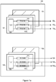
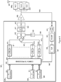
- FIG. 1 shows a digital radio module 100 according to an embodiment of the invention.
- the digital radio module 100 comprises a modular architecture for use in a multi-band multi-standard radio communication apparatus.
- the digital radio module 100 comprises one or more digital transmitter sub modules 101 1 to 101 X , each digital transmitter sub module comprising a plurality of digital transmitter chains 103 1 to 103 N .
- the digital radio module 100 also comprises one or more digital receiver sub modules 105 1 to 105 Y , each digital receiver sub module comprising a plurality of digital receiver chains 107 1 to 107 M .
- Each of the digital transmitter sub modules 101 1 to 101 X and digital receiver sub modules 105 1 to 105 Y comprises a respective control unit 109 for individually configuring each digital transmitter sub module and digital receiver sub module such that the digital radio module 100 is operable to transmit and/or receive multiple different carrier frequency signals in one or more different modes of operation.
- the modular architecture By providing a modular architecture having transmitter and receiver sub modules, each being configurable in its own right, this has the advantage of providing a highly integrated multi-band multi-standard radio (MSR) Digital Radio Module (DRM), which can support at least one pair of TX/RX antennas.
- MSR multi-band multi-standard radio
- DRM Digital Radio Module
- the modular architecture enables a highly frequency agnostic digital radio module to be provided ("agnostic" meaning in this context that the performance of the module does not depend on the frequencies on which it operates).
- the embodiments of the invention can support:
- the modular architecture enables the interconnections between the components to be kept short, such that power consumption generated in the interconnections between the components inside the digital radio module can be reduced.
- Long lines and connectors have large parasitic capacitance and thus power consumption is increased by the need to drive these parasitic capacitors. Therefore, by keeping the transmission lines short according to the modular architecture of the embodiments of the invention, low power drivers can be used in order to lower the power dissipation in the device.
- Another benefit is an improved frequency response for the radio communication apparatus which is achieved by the lower capacitances and inductances in the interconnections between the sub modules of the modular architecture.
- the digital radio module is multi-band (or effectively frequency agnostic) and multi-standard it can be used in any base station radio unit.
- the embodiments of the invention can also be used in other radio communication enabled apparatus. It is noted that more than one DRM can be used in radio implementations such as an array antenna with active antenna elements, in order to achieve wanted functionality and performance.
- each sub module also includes transmitter and/or receiver characterization capabilities.
- a digital transmitter sub module and a digital receiver sub module may be combined into a transmitter/receiver sub module, with a common control unit 109 for controlling the combined transmitter/receiver sub module.
- a common control unit 109 for controlling the combined transmitter/receiver sub module.
- one or more of the control units may be combined into a central control unit that is configured to control one or more of the digital transmitter sub modules or digital receiver sub modules.
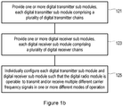
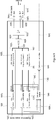
- Figure 1b illustrates a method according to an embodiment of the invention, for a digital radio module that comprises a modular architecture for use in a multi-band multi-standard radio communication apparatus that is operable over a wide frequency range.
- the method comprises the step of providing one or more digital transmitter sub modules, each digital transmitter sub module comprising a plurality of digital transmitter chains, step 121, and providing one or more digital receiver sub modules, each digital receiver sub module comprising a plurality of digital receiver chains, step 123.
- the method further comprises the step of individually configuring each digital transmitter sub module and digital receiver sub module such that the digital radio module is operable to transmit and/or receive multiple different carrier frequency signals in one or more different modes of operation, step 125.
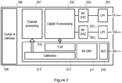
- FIG. 2 shows an example of a digital transmitter sub module that may be used in a digital radio module according to an embodiment of the present invention.
- the digital transmitter 200 can be coupled during use to receive a digital representation of a respective base band signal.
- a control and interface unit 209 enables the transmitter sub module 200 to be individually configured such that the transmitter sub module is operable to transmit multiple different carrier frequency signals in one or more different modes of operation.
- a digital transmitter processing unit 205 is provided, as discussed in greater detail later in the application, to up-convert a plurality of digital baseband signals directly to a plurality of digital radio frequency signals, for example using Direct Radio Frequency Technology, DRF.
- Each digital RF signal is fed to a RF digital to analogue converter 203 that is adapted to convert the digital radio frequency signal into an analogue radio frequency signal, which is fed to a respective low pass filter 201.
- a digital combining unit can be provided for combining digital radio frequency signals, on different frequency bands for the same antenna, from the digital transmitter processing unit 205
- the digital transmitter processing unit 205 is therefore coupled to receive multiple base band carrier signals from the same or different frequency bands, and is adapted to digitally process the multiple base band carrier signals to produce a digital representation of each base band signal for each of the digital transmitter chains.
- the digital transmitter processing unit 205 may be configured to perform processing tasks such as crest factor reduction (CFR, CFAR) or digital pre-distortion (DPD). Other processing tasks may also be performed by the processing unit 205.
- the transmitter sub module 200 further comprises a feedback unit 211 coupled to monitor an output signal of the transmitter sub module, for example by taking the output of a power amplifier (not shown), or an antenna (also not shown), and adapted to provide a feedback signal to the digital transmitter processing unit 205 and a channel processing unit 207.
- the feedback unit 211 comprises a digital receiver 217 (for example a DRF receiver) coupled to the output of a power amplifier (or antenna) via a high speed radio frequency ADC 219.
- the feedback unit 211 also comprises a transmitter observation receiver 215, TOR, coupled to receive an output of the digital receiver 217. As such, a measurement signal, decoupled at the power amplifier (or antenna after the power amplifier) is fed to a digital TOR for RF signal characterization.
- the characterized RF signal is fed as a feedback signal into the digital transmitter processing unit 205.
- the function of the digital TOR 215 will be familiar to a person skilled in the art, and is for example described in a paper entitled “ Linearizing Power Amplifiers Using Digital Predistortion, EDA Tools and Test Hardware", by Kelly Mekechuk et al, April 2004, High Frequency Electronics journal .
- the TOR 215 preferably comprises a frequency agile multiband capability, for example a wideband reduced dynamic range version of a DRF receiver, such that it can measure the output signal of the transmitter, including the distortion components.
- the TOR 215 can be a digital TOR (DTOR). This DTOR is reused for all carriers in all frequency bands.
- this embodiment of the invention has the advantage of enabling a common DTOR to be used for the multiple frequency band signals, within a digital transmitter sub module.
- the transmitter sub module 200 is configured such that unwanted RF signals from the DACs 203 are filtered out by the filter units 201.
- the low pass filter units 201 can be realised as a common filter unit, for example a filter unit that performs an anti aliasing filtering function.
- the transmitter sub module 200 comprises a channel processing unit 207, which is adapted to process a plurality of base band carriers prior to being processed by the digital transmitter processing unit 205.
- the channel processing unit 207 is configured to perform, for example, PreCoder functions or Inverse Fast Fourier Transforms (IFFT) on the base band signals.
- IFFT Inverse Fast Fourier Transforms
- the channel processing unit 207 is fed by base band signals, for different carriers and frequency bands.
- the channel processing unit 207 receives feedback signals from a calibration unit 213.
- the transmitter sub module of Figure 2 therefore comprises:
- FIG. 3 shows an example of a digital receiver sub module that may be used in a digital radio module according to an embodiment of the present invention.
- Each digital receiver chain is coupled to receive a digital representation of the multiple radio frequency bands, including a particular radio frequency band for processing by the respective digital receiver chain.
- Each digital receiver chain comprises a digital receiver that is programmable to select a particular radio frequency band from the digital representation of the multiple radio frequency bands, and adapted to down convert the selected radio frequency band into a digital baseband signal associated with the particular radio frequency band, for example using DRF technology.
- the digital receivers of each chain are represented by the receiver unit 301 in Figure 3 .
- the receiver sub module 300 comprises a digital receiver processing unit 303 that is coupled to receive the outputs of the digital receiver unit 301, and adapted to process the digital signals to provide the digital baseband output signals.
- the digital receiver processing unit 303 may comprise either separate units for each digital receiver chain, or comprise a common processing unit that processes signals in each of the digital receiver chains.
- the receiver sub module 300 further comprises a calibration unit 307 comprising a calibration receiver 319.
- a calibration signal from a coherence calibration unit 307 is transmitted by a transmitter unit 315, for example a DRF transmitter, to a DAC 313 which converts the calibration signal into analogue form for use in calibrating the receiver apparatus, for example by injecting the calibration signal into the input of the receiver, e.g. via an antenna unit (not shown).
- the output of the RF-DAC 313 may be filtered by a low pass filter 311. Further details about the operation of the calibration unit are provided below, in relation to the embodiments of Figures 6 and 9 .
- a control and interface unit 309 comprises a control unit (not shown) that enables the receiver sub module to be individually configured such that the receiver sub module is operable to receive multiple different carrier frequency signals in one or more different modes of operation.
- the receiver sub module according to the embodiment of Figure 3 comprises:
- An implementation of a radio unit and its capabilities are defined by means of the number of transmitter and receiver sub modules which are integrated into digital radio modules, that are used in a particular implementation.
- a digital radio module can therefore be defined by means of the number of transmitter and receiver sub modules that are used in a specific application. Different implementations of a radio unit may thus use different DRM modules but the same sub modules.
- a radio unit does not have to be symmetrical, which means that some application can have more transmit antennas than receive antennas, or vice verse. Thus, by having different modules for TX and RX it is possible to optimize the amount of hardware needed for a particular implementation and thus reduce the cost.
- Such a radio unit 400 comprises a plurality of transmitter sub modules 200 and a plurality of receiver sub modules 300.
- the radio unit comprises:
- the timing unit is provided because it is important that all signals have the same time reference so that the transmission of signals is performed at the same time +/- dt related to a frame synchronisation, (which are 3 GPP requirements for MIMO and TX diversity).
- the timing unit is also required for RF coherence, which means that RF from different transmitters are synchronous with some controlled relative phase shift to each other. In order to maintain this coherence it is required that all transmitters have the same time reference.
- a radio unit In an implementation of a radio unit a plurality of digital radio modules, array of Multi band power amplifiers, RF filters and antennas, can be used in order to achieve wanted functionality and performance.
- FIG. 5 A further example of an embodiment of a transmitter sub module based on DRF technology is shown in Figure 5 .
- FIG. 5 shows a plurality of digital transmitter sub modules 501 (only two 501 1 and 501 2 being shown for clarity) that can form part of a digital radio module 500.
- Each transmitter sub module 501 is operable to transmit multiple radio frequency bands in a telecommunication system, and comprises a plurality of digital transmitter chains 523 1 to 523 K .
- Each digital transmitter chain is coupled to receive a digital representation of a respective base band signal.
- Each digital transmitter chain 523 1 to 523 K comprises a digital transmitter that is configured to up-convert a digital baseband signal directly to a digital radio frequency signal, for example using Direct Radio Frequency Technology, DRF.
- DRF Direct Radio Frequency Technology
- a digital combining unit 525 for example a digital summing unit, is coupled to receive the output of each digital transmitter chain 523 1 to 523 K , and adapted to combine the digital radio frequency signals received from each digital transmitter chain 523 1 to 523 K into a digital radio frequency signal comprising multiple radio frequency bands.
- a digital to analogue converter 543 is coupled to receive the digital radio frequency signal comprising multiple radio frequency bands, and adapted to convert the digital radio frequency signal into an analogue radio frequency signal comprising multiple radio frequency bands.
- the transmitter sub module 501 further comprises a common processing unit 530.
- the common processing unit 530 is coupled to receive multiple base band carrier signals, and is adapted to digitally process the multiple base band carrier signals to produce the digital representation of each base band signal for each of the digital transmitter chains.
- the multi band transmitter is fed by base band carrier signals, for different carriers and frequency bands, to the common processing block 530.
- the common processing block may be configured to perform processing tasks such as crest factor reduction (CFR, CFAR) or digital pre-distortion (DPD) algorithms.
- CFR, CFAR crest factor reduction
- DPD digital pre-distortion
- the processed (or corrected) base band signal for each frequency band is then fed to a respective DRF digital transmitter that digitally converts the base band signal to digital RF in the right frequency band.
- the digital RF signals from different frequency bands are combined in the digital combining unit 525 into one signal that is fed to a high speed DAC 527.
- the transmitter sub module 501 of Figure 5 further comprises a digital pre-distortion actuator unit 533 (DPD) coupled between the digital combining unit 525 and the digital to analogue converter 527.
- DPD digital pre-distortion actuator unit
- the digital pre-distortion unit 533 is configured to modify the digital radio frequency signal comprising multiple radio frequency bands prior to conversion by the digital to analogue converter 527.
- the digital pre-distortion unit 533 is configured to deal with characteristics of the multiple bands, such as the spacing between bands, the width of each band, the frequency range of each band, and so forth.
- a look-up table 535 (LUT) is provided for controlling the operating parameters of the digital pre-distortion unit 533, wherein the look-up table is controlled by the common processing unit 530 using a control signal, for example a feedback signal from a feedback unit 541.
- the feedback unit 541 is coupled to monitor an output signal of the transmitter sub module, for example by taking the output of a power amplifier 529, and adapted to provide a feedback signal to the common processing unit 530 of each transmitter sub module 501. Alternatively, the feedback unit 541 can derive its input signal by coupling to a transmit antenna 547 that is fed by the power amplifier 529.
- the feedback unit 541 comprises a digital receiver 537 (for example a DRF receiver) coupled to the output of the power amplifier 529 (or antenna) via a high speed radio frequency ADC 539.
- a selector unit 536 is provided for selecting which feedback signal is to be used.
- the feedback unit 541 also comprises a transmitter characterisation receiver 538, TCR, coupled to receive an output of the digital receiver 537.
- TCR transmitter characterisation receiver
- a measurement signal decoupled at the power amplifier (or antenna after the power amplifier) is fed to a digital TCR for RF signal characterization.
- the characterized RF signal is fed as a feedback signal into the common processing unit 530 for DPD processing.
- the function of the digital TCR 538 will be familiar to a person skilled in the art.
- the transmitter sub module 501 is further adapted such that unwanted RF signals from the DAC 527 are filtered out in a common filter unit 543, for example a filter unit that performs an anti aliasing filtering function.
- the transmitter sub module 501 therefore comprises a wide band filter unit 543 coupled to the output of the digital to analogue converter 527, the wide band filter unit 543 being adapted to perform an anti aliasing function on the analogue radio frequency signal comprising multiple radio frequency bands.
- the wide band filter unit 543 has the advantage of being physically small and low cost (that is, small or having an insignificant size in relation to the DAC and the overall transmitter implementation).
- the transmitter apparatus may further comprise a plurality of output filter units, for example provided in a common filter unit 545, coupled to the output of the wide band power amplifier 529.
- Each of the plurality of output filter units is adapted to receive the amplified analogue radio frequency signal comprising multiple radio frequency bands, and adapted to filter a required radio frequency band for coupling to an antenna 547.
- the frequency specific output filter units filter out respective wanted RF signals, which are combined and fed to the transmitter antenna 547.
- the transmitter sub module 501 further comprises a plurality of base band carrier processing units 549 1 to 549 J , where J equals the number of carriers, each base band carrier processing unit adapted to process a base band carrier signal prior to being processed by the common processing unit 530.
- the plurality of base band carrier processing units 549 1 to 549 J may perform, for example, PreCoder functions or Inverse Fast Fourier Transforms (IFFT) on the base band signals.
- IFFT Inverse Fast Fourier Transforms
- the plurality of base band carrier processing units 549 1 to 549 J are fed by base band signals, for different carriers and frequency bands. Further base band processing may be provided by a transmitter base band processing unit 550.
- the common processing unit 530 comprises a control unit (not shown) that enables the transmitter sub module 501 to be individually configured such that the transmitter sub module is operable to transmit multiple different carrier frequency signals in one or more different modes of operation.
- one end (the left side) is connected to base band and at the other end (right side) connected to a RF power amplifier that handles all carriers.
- a feedback signal from either the power amplifier 529 or from the antenna element 547 is connected to the common transmitter characterization receiver (TCR) for Digital Pre- Distortion (DPD) and calibration measurements.
- TCR common transmitter characterization receiver
- DPD Digital Pre- Distortion
- the feedback signal to the TCR is selected by means of an analogue selector 536.
- the feedback signal from the power amplifier 529 is used for DPD measurements and the feedback signal from the antenna element 547 is used for calibration measurements.
- the transmitter architecture supports N logical transmitter chains and comprises N transmitter processing blocks in the form of a Common TX (CTX) processing block, N TX-DRF blocks, a RF-DAC, an anti-aliasing filter that is divided into two parts, a low pass and and a high pass filter, a wide band power amplifier 529 and N transmitter filters.
- the band pass filter is divided into two parts in order to achieve a frequency agnostic DRM.
- DTOR Digital Transmit Observation Receiver
- There is one transmitter chain per supported antenna where each chain supports K frequency bands and J carriers, where N is the number of antennas or unique signal paths, K is the number of frequency bands, and J is the number of carriers that can be transmitted in each frequency band.
- the digital transmitter sub module of the embodiment of Figure 5 comprises:
- the transmitter characterization receiver, TCR, 541 is a shared resource for calibration and power amplifier linearization measurements.
- One signal for calibration measurements is decoupled at the antenna after a combiner, and a feedback signal from the output of the power amplifier 529 is fed to the TCR 541 for RF signal characterization in the transmitter observation transmitter calibration block.
- the characterization receiver is configured to operate in two modes, one for linearization and one for calibration purposes.
- the input signal is selected by integrated switches, using the selector block 536.
- the characterized RF signal is fed into the common transmitter processing block 530 of each transmitter sub module 501 for CFR and DPD processing.
- the TCR 541 is reused for all carriers in all frequency bands.
- the TCR 541 uses reference signals (not shown) from the common transmitter processing block.
- the TCR block 541 that measures the RF quality, based on the reference signal, on each of the J carriers at the physical antenna port, comprises a high speed ADC 539, Receiver DRF 537 and signal signature characterization for DPD and calibration usage.
- FIG. 6 shows a receiver 600 comprising a plurality of receiver sub modules according to another embodiment of the present invention.
- Each receiver sub module comprises a plurality of digital receiver chains 625 1 to 625 K , each digital receiver chain 625 1 to 625 K coupled to receive a digital representation of the multiple radio frequency bands (from a receiver interface 629), including a particular radio frequency band for processing by the respective digital receiver chain.
- Each digital receiver chain 625 1 to 625 K comprises a digital receiver that can be programmed to select a particular radio frequency band from the digital representation of the multiple radio frequency bands, and adapted to down convert the selected radio frequency band into a digital baseband signal associated with the particular radio frequency band, for example using DRF technology.
- Each digital receiver chain in a sub module comprises a digital processing unit 637 1 to 637 K coupled to receive the output of a respective digital receiver, and adapted to process the digital signal to provide the digital baseband output signal.
- the digital processing units may either be separate units for each digital receiver chain, or part of a common processing unit that processes signals in each of the digital receiver chains.
- the receiver sub module 600 further comprises a calibration stage comprising a calibration receiver 640 and a calibration transmitter 641.
- the calibration stage is configured to correct the I and Q signals at a base band level, and in particular one or more of phase, amplitude or delay in the respective digital receiver chains in order to achieve RF coherence.
- the calibration receiver 640 is configured to generate a calibration signal which is transmitted using the calibration transmitter 641 into the incoming signal path of the receiver, for example into an antenna (not shown) which feeds the receiver.
- the same calibration signal is detected in each of the digital receiver chains 625 1 to 625 K and coupled as a set of feedback signals, or measured signals to the input of the calibration receiver 640, thereby providing feedback signals to the calibration receiver 640.
- the calibration signal is detected or measured in each of the digital chains 625 1 to 625 K using the plurality of digital processing units 637 1 to 637 K , with the measured signals being coupled to the input of the calibration receiver 640.
- the measured signals received by the calibration receiver 640 are compared with each other, for example using a MSR receiver, with one or more of phase, amplitude and delay parameters being calculated relative to one of the receiver signals.
- the phase, amplitude and delay of each of the received calibration signals are compared with one of the received calibration signals, for example all compared with the calibration signal received from a first digital receiver chain.
- Correction parameters are then determined, and used to adjust the phase, amplitude and/or delay parameters of one or more of the respective outputs of the digital receivers in the digital receiver chains 625 1 to 625 K , according to the result of the comparison step.
- the adjusting operation may comprise adding or subtracting correction parameters to the outputs of one or more of the digital receivers. For example, if the comparison process is made with respect to the output of digital receiver 625 1 , then correction parameters are added or subtracted to the phase, amplitude and/or delay of one or more of the output signals of digital receivers 625 2 to 625 K .
- this enables RF coherence to be achieved between the different digital receiver chains.
- Figure 6 also shows a filter unit 645 that is configured to receive a radio signal including the multiple radio frequency bands, in analogue form, for example from one or more antennas 660.
- the filter unit 645 comprises a plurality of filters 645 1 to 645 K for separating the received radio signal into multiple analogue radio frequency signals. It is noted that these filters, for example bandpass filters, can be arranged as separate filters or as an array of switchable filters, in the filter unit or bank 645.
- a plurality of amplifier units 647 can be provided (for example low noise amplifiers, LNAs), the plurality of amplifier units 647 being coupled to receive the multiple analogue radio frequency signals and amplify the analogue radio frequency signals prior to being processed by the receiver interface 629. This has the advantage of improving the signal to noise level.
- LNAs low noise amplifiers
- a common amplifier unit (such as a common LNA) may be provided instead of band specific amplifier units.
- FIG. 6 therefore shows a multi band multi antenna receiver block which is connected to the logical receiver path in the digital radio module.
- the receivers may be implemented as digital domain receivers utilizing Direct Radio Frequency (DRF) technology.
- DRF Direct Radio Frequency
- the input signal from the antenna/filter is converted to the digital domain by means of an ADC that is transferred to a digital processing block where the virtual receivers are implemented.
- the receivers 625 of Figure 6 are connected to an receiver processing block 637 where receiver signal correction, channelizing and filtering for each carrier and antenna signal is performed.
- the signal correction parameters are calculated in the receiver calibration block 640.
- the receiver processing block also detects the measurement signal, used for calibration, that is generated in the Receiver Calibration Transmitter (RCT) 644 and injected into each RF signal in the path for each receiver.
- the detected feedback signal, from each receiver, is transferred to the RCT 644, for calculation of correction parameters.
- FIG. 7 A further example of a architecture of a receiver part of a digital radio module, according to another embodiment, is shown in Figure 7 .
- An antenna block 760 comprises a plurality of filter banks 745 for filtering a received signal into a plurality of analogue RF signals for each respective receiver sub module.
- the analogue RF signals are converted to digital format by respective ADC's 729 for each receiver sub module.
- Each receiver sub module comprises a plurality of digital receiver chains, each comprising a digital receiver 725 1 to 725 K , such as a DRF receiver, for converting the digital RF signals into base band signals.
- Figure 7 shows a common linearization block 769 for all of the digital receiver sub modules, with feedback signals being selected by a selector block 735.
- FIG 8 shows an example of a transmitter sub module that may be used in a digital radio module according to another embodiment of the present invention.
- the transmitter sub module 920 is operable to transmit multiple radio frequency bands in a telecommunication system, and comprises a plurality of digital transmitter chains 921 1 to 921 N .
- Each digital transmitter chain is coupled to receive a digital representation 927 1 to 927 N of a respective base band signal.
- Each digital transmitter chain 921 1 to 921 N comprises a digital transmitter 925 1 to 925 N that is configured to up-convert a digital baseband signal directly to a digital radio frequency signal 923 1 to 923 N .
- the digital transmitter 925 1 to 925 N of Figure 9 may comprise a digital transmitter that is configured to up-convert a digital base band signal directly to a radio frequency signal using Direct Radio Frequency Technology, DRF.
- DRF Direct Radio Frequency Technology
- a digital combining unit 925 for example a digital summing unit, is coupled to receive the output of each digital transmitter chain 921 1 to 921 N , and adapted to combine the digital radio frequency signals 923 1 to 923 N received from each digital transmitter chain 921 1 to 921 N into a digital radio frequency signal 926 comprising multiple radio frequency bands.
- a digital to analogue converter 927 is coupled to receive the digital radio frequency signal 926 comprising multiple radio frequency bands, and adapted to convert the digital radio frequency signal 926 into an analogue radio frequency signal 928 comprising multiple radio frequency bands.
- the transmitter sub module 920 further comprises a common processing unit 930.
- the common processing unit 930 is coupled to receive multiple base band carrier signals 931 1 to 931 N , and is adapted to digitally process the multiple base band carrier signals to produce the digital representation 929 1 to 929 N of each base band signal for each of the digital receiver chains.
- the multi band transmitter is fed by base band carrier signals, for different carriers and frequency bands, to the common processing block 930.
- the common processing block may be configured to perform processing tasks such as crest factor reduction (CFR, CFAR) or digital pre-distortion (DPD).
- CFR, CFAR crest factor reduction
- DPD digital pre-distortion
- the processed (or corrected) base band signal for each frequency band is then fed to a respective DRF digital transmitter that digitally converts the base band signal to digital RF in the right frequency band.
- the digital RF signals from different frequency bands are combined in the digital combining unit 925 into one signal 926 that is fed to the high speed DAC 927.
- the transmitter sub module 920 of Figure 9 further comprises a digital pre-distortion unit 933 (DPD) coupled between the digital combining unit 925 and the digital to analogue converter 927.
- the digital pre-distortion unit 933 is configured to modify the digital radio frequency signal 926 comprising multiple radio frequency bands prior to conversion by the digital to analogue converter 927.
- the digital pre-distortion unit 933 is configured to deal with characteristics of the multiple bands, such as the spacing between bands, the width of each band, the frequency range of each band, and so forth.
- a look-up table 935 (LUT) is provided for controlling the operating parameters of the digital pre-distortion unit 933, wherein the look-up table is controlled by the common processing unit 930 using a control signal 936.
- the control signal 936 may be based on a feedback signal received by the common processing unit 930.
- the transmitter sub module 920 further comprises a feedback unit 941 coupled to monitor an output signal of the transmitter sub module, for example by taking the output of a power amplifier 929, and adapted to provide a feedback signal 940 to the common processing unit 930.
- the feedback unit 941 can derive its input signal by coupling to a transmit antenna (not shown) that is fed by the power amplifier 929.
- the feedback unit 941 comprises a digital receiver 937 (for example a DRF receiver) coupled to the output of the power amplifier 929 (or antenna) via a high speed radio frequency ADC 939.
- the feedback unit 941 also comprises a transmitter observation receiver 938, TOR, coupled to receive an output of the digital receiver 937.
- a measurement signal, decoupled at the power amplifier (or antenna after the power amplifier) is fed to a digital TOR for RF signal characterization.
- the characterized RF signal is fed as a feedback signal 940 into the common processing unit 930 for DPD processing.
- the function of the digital TOR 938 will be familiar to a person skilled in the art.
- the TOR 938 preferably comprises a frequency agile multiband capability, for example a wideband reduced dynamic range version of a DRF receiver, such that it can measure the output signal of the transmitter, including the distortion components. It is noted that the dynamic range can be reduced relative to an ordinary RBS receiver as the transmitter signal is measured directly at the output of the transmitter without the additional path loss added in a real system.
- the TOR 938 can be a digital TOR (DTOR). This DTOR is reused for all carriers in all frequency bands. Thus, this embodiment of the invention has the advantage of enabling a common DTOR to be used for the multiple frequency band signals. Reference signals from a common TX processing block are not shown in Figure 8 for clarity purposes.
- DTOR digital TOR
- the transmitter sub module 920 is further adapted such that unwanted RF signals from the DAC 927 are filtered out in a common filter unit 943, for example a filter unit that performs an anti aliasing filtering function.
- the transmitter sub module 920 therefore comprises a wide band filter unit 943 coupled to the output of the digital to analogue converter 927, the wide band filter unit 943 being adapted to perform an anti aliasing function on the analogue radio frequency signal 928 comprising multiple radio frequency bands.
- the wide band filter unit 943 has the advantage of being physically small and low cost (that is, small or having an insignificant size in relation to the DAC and the overall transmitter implementation).
- the transmitter sub module 920 may further comprise a plurality of output filter units 945 1 to 945 N coupled to the output of a wide band power amplifier 929.
- Each of the plurality of output filter units is adapted to receive the amplified analogue radio frequency signal 928 comprising multiple radio frequency bands, and adapted to filter a required radio frequency band for coupling to an antenna 947.
- the frequency specific output filter units filter out respective wanted RF signals, which are combined and fed to the transmitter antenna 947.
- the power amplifier 929 and filters can be separate entities while the filters can be seen as a sub module with at least one filter unit. By having several filters in the filter sub module the system can be prepared to handle several frequency bands.
- the transmitter sub module 920 further comprises a plurality of base band carrier processing units 949 1 to 949 N , each base band carrier processing unit adapted to process a base band carrier signal prior to being processed by the common processing unit 930.
- the plurality of base band carrier processing units 949 1 to 949 N may perform, for example, PreCoder functions or Inverse Fast Fourier Transforms (IFFT) on the base band signals.
- IFFT Inverse Fast Fourier Transforms
- the plurality of base band carrier processing units 949 1 to 949 N are fed by base band signals, for different carriers and frequency bands.
- the common processing unit 930 comprises a control unit (not shown) that enables the transmitter sub module to be individually configured such that the transmitter sub module is operable to transmit multiple different carrier frequency signals in one or more different modes of operation.
- each digital transmitter chain comprises a digital transmitter that is configured convert a respective digital base band signal directly into a digital radio frequency signal
- the digital transmitter sub module comprising a digital combining unit coupled to receive the output of each digital transmitter chain, and adapted to combine the digital radio frequency signal received from each digital transmitter chain into a digital radio frequency signal comprising multiple radio frequency bands
- a digital to analogue converter coupled to receive the digital radio frequency signal comprising multiple radio frequency bands, and adapted to convert the digital radio frequency signal into an analogue radio frequency signal comprising multiple radio frequency bands.
- the digital transmitter sub module of Figure 8 further comprises a common processing unit, the common processing unit coupled to receive a plurality of base band carrier signals, and adapted to digitally process the plurality of base band carrier signals to produce the digital representation of each base band signal for each of the digital transmitter chains.
- a digital pre-distortion unit, DPD coupled between the digital combining unit and the digital to analogue converter, is provided for modifying the digital radio frequency signal comprising multiple radio frequency bands prior to conversion by the digital to analogue converter.
- a common characterization and/or linearization unit is provided for the plurality of digital transmitter sub modules, wherein the common characterization and/or linearization unit is adapted to monitor the output of a power amplifier or antenna being fed by a digital transmitter sub module, and adapted to provide feedback signals to the common processing unit.
- the common characterization and/or linearization unit comprises: a digital receiver coupled to the output of the power amplifier or antenna; and a transmitter observation receiver coupled to receive an output of the digital receiver, and provide the feedback signals to the common processing unit.
- FIG. 9 shows a receiver sub module 1020 according to another embodiment of the present invention.
- the receiver sub module 1020 comprises a plurality of digital receiver chains 1021 1 to 1021 K , each digital receiver chain 1021 1 to 1021 K coupled to receive a digital representation 1023 of the multiple radio frequency bands, including a particular radio frequency band for processing by the respective digital receiver chain.
- Each digital receiver chain 1021 1 to 1021 K comprises a digital receiver 1025 1 to 1025 K that is programmable to select a particular radio frequency band from the digital representation 1023 of the multiple radio frequency bands, and adapted to down convert the selected radio frequency band into a digital baseband signal 10271 1 to 1027 K associated with the particular radio frequency band, for example using DRF technology.
- the radio communication receiver apparatus 1020 comprises an analogue to digital converter 1029 coupled to receive an analogue signal 1031 comprising the multiple radio frequency bands, and adapted to output the digital representation 1023 of the multiple radio frequency bands to each digital receiver chain 1021 1 to 1021 K .
- the receiver sub module 1020 comprises a combining unit 1033 coupled to receive analogue radio frequency signals 1035 1 to 1035 K , and adapted to combine the multiple analogue radio frequency signals 1035 1 to 1035 K into the analogue signal 1031 comprising multiple radio frequency bands for processing by the analogue to digital converter 1029.
- a combining unit 1033 coupled to receive analogue radio frequency signals 1035 1 to 1035 K , and adapted to combine the multiple analogue radio frequency signals 1035 1 to 1035 K into the analogue signal 1031 comprising multiple radio frequency bands for processing by the analogue to digital converter 1029.
- separate analogue to digital converters may be provided in each digital receiver chain, each analogue to digital converter being adapted to receive an analogue signal 1031 comprising the multiple radio frequency bands, and adapted to output the digital representation 1023 of the multiple radio frequency bands to its respective digital receiver chain 1021 1 to 1021 K .
- Each digital receiver chain in the receiver sub module 1020 comprises a digital processing unit 1037 1 to 1037 K coupled to receive the output of a respective digital receiver 1025 1 to 1025 K , and adapted to process the digital signal to provide the digital baseband output signal 1027 1 to 1027 K .
- the digital processing units may either be separate units for each digital receiver chain, or part of a common processing unit that processes signals in each of the digital receiver chains.
- the receiver sub module 1020 further comprises a calibration stage comprising a calibration receiver 1040 and a calibration transmitter 1041.
- the calibration stage is configured to correct the I and Q signals at a base band level, and in particular one or more of phase, amplitude or delay in the respective digital receiver chains in order to achieve RF coherence.
- the calibration receiver 1040 is configured to generate a calibration signal 1043 which is transmitted using the calibration transmitter 1041 into the incoming signal path of the receiver 1020, for example into an antenna (not shown) which feeds the combining unit 1033.
- the same calibration signal is detected in each of the digital receiver chains 1021 1 to 1021 K and coupled as a set of feedback signals, or measured signals 1039 1-K to the input of the calibration receiver 1040, thereby providing feedback signals to the calibration receiver 1040.
- the calibration signal is detected or measured in each of the digital chains 1021 1 to 1021 K using the plurality of digital processing units 1037 1 to 1037 K , with the measured signals 1039 1-K being coupled to the input of the calibration receiver 1040.
- the measured signals 1039 1-K received by the calibration receiver 1040 are compared with each other, for example using a MSR receiver, with one or more of phase, amplitude and delay parameters being calculated relative to one of the receiver signals.
- the phase, amplitude and delay of each of the received calibration signals are compared with one of the received calibration signals, for example all compared with the calibration signal received from the first digital receiver chain 1021 1 .
- Correction parameters 1042 1-K are then determined, and used to adjust the phase, amplitude and/or delay parameters of one or more of the respective outputs of the digital receivers 1025 1 to 1025 K , according to the result of the comparison step.
- the adjusting operation may comprise adding or subtracting correction parameters to the outputs of one or more of the digital receivers 1025 1 to 1025 K .
- correction parameters are added or subtracted to the phase, amplitude and/or delay of one or more of the output signals of digital receivers 1025 2 to 1025 K .
- the calibration process can be run during a calibration mode of operation, during which the calibration signal 1043 is used to determine what correction parameters, if any, are needed to the various digital receiver chains. These correction parameters are then used to correct the different frequency band signals based on the actual working of the various digital receiver chains.
- the calibration mode of operation can be run periodically, and the correction parameters set accordingly.
- the calibration stage is therefore adapted, during a calibration mode of operation, to transmit a calibration signal to the input of the receiver apparatus, and adapted to detect the phase, amplitude and/or delay of the calibration signal after being converted to a baseband signal in each digital receiver chain 1021 1 to 1021 K .
- the detected signal from each digital receiver chain provides a set of feedback signals for use by the calibration stage to define a set of correction parameters, wherein the set of correction parameters are used by the digital processing unit 1037 1 to 1037 K to adjust one or more of the phase, amplitude and/or delay of a base band signal in one or more of the digital receiver chains.
- the calibration stage comprises a calibration transmitter for coupling the calibration signal to an input of the receiver, and a calibration receiver for receiving the set of feedback signals from each digital receiver chain, wherein the calibration receiver is adapted to compare the phase, amplitude and/or delay of each of the set of feedback signals, and determine the set of correction parameters based on the comparison.
- the receiver sub module 1020 further comprises a filter unit 1045.
- the filter unit 1045 is configured to receive a radio signal including the multiple radio frequency bands, in analogue form, for example from one or more antennas.
- the filter unit 1045 comprises a plurality of filters fb1 to fbK for separating the received radio signal into multiple analogue radio frequency signals 1035 1 to 1035 K . It is noted that these filters, for example bandpass filters, can be arranged as separate filters or as an array of switchable filters, in the filter unit or bank 1045.
- a plurality of amplifier units 1047 1 to 1047 K can be provided (for example low noise amplifiers, LNAs), the plurality of amplifier units 1047 1 to 1047 K being coupled to receive the multiple analogue radio frequency signals 1035 1 to 1035 K and amplify the analogue radio frequency signals 1035 1 to 1035 K prior to being combined by the combining unit 1033.
- LNAs low noise amplifiers
- a common amplifier unit 1047 (such as a common LNA) may be provided instead of band specific amplifier units 1047 1 to 1047 K .
- the summation or combining can be made by providing an RF combining unit at the input of the common amplifier unit 1047 (for example at the input of a common LNA).
- the embodiment above provides a receiver sub module architecture that comprises K digital receiver (DRX) chains 1021 1 to 1021 K , comprising Receiver Carrier (RXC) processing blocks 1037 1 to 1037 K , and direct radio frequency receivers (RX-DRF blocks) 1025 1 to 1025 K , a common RF-ADC 1029 for all digital receiver chains 1021 1 to 1021 K .
- the receiver comprises a filter bank 1045 that defines the receiver frequency bands. For calibration a calibration stage is provided.
- an analogue to digital converter could be used for each frequency band according to an alternative embodiment, and thus, in which case there is no need for received signals to be combined after the band filters, before connecting to each ADC.
- each digital receiver chain is coupled to receive a digital representation of multiple radio frequency bands, including a particular radio frequency band for processing by the respective digital receiver chain, wherein each digital receiver chain comprises a digital receiver that is programmable to select a particular radio frequency band from the digital representation of the multiple radio frequency bands, and adapted to down convert the selected radio frequency band into a digital baseband signal associated with the particular radio frequency band.
- the digital receiver sub module further comprises an RF analogue to digital converter coupled to receive an analogue signal comprising the multiple radio frequency bands, which is adapted to output the digital representation of the multiple radio frequency bands to each digital receiver chain.
- a combining unit is coupled to receive multiple analogue radio frequency signals, and adapted to combine the multiple analogue radio frequency signals into the analogue signal comprising multiple radio frequency bands for processing by the RF analogue to digital converter.
- a digital processing unit is coupled to receive the output of each digital receiver, and adapted to process the output of each digital receiver to provide a digital baseband output signal.
- the digital processing unit can form part of a common digital processing unit that is common to all digital receiver chains in a particular digital receiver sub module.
- the digital receiver sub module further comprises a calibration stage that is adapted during a calibration mode of operation to transmit a calibration signal to the input of the digital receiver sub module, and adapted to detect the phase, amplitude and/or delay of the calibration signal after being converted to a baseband signal in each digital receiver chain, the detected signal from each digital receiver chain providing a set of feedback signals for use by the calibration stage to define a set of correction parameters, wherein the set of correction parameters are used by the digital processing unit to adjust one or more of the phase, amplitude and/or delay of a base band signal in one or more of the digital receiver chains.
- the calibration stage comprises: a calibration transmitter for coupling the calibration signal to an input of the digital receiver sub module; a calibration receiver for receiving the set of feedback signals from each digital receiver chain, wherein the calibration receiver is adapted to compare the phase, amplitude and/or delay of each of the set of feedback signals, and determine the set of correction parameters based on the comparison.
- the embodiments of the invention also provide a frequency agnostic transmitter and a frequency agnostic receiver. They provide a multi band multi carrier transmitter and multi antenna, utilizing the same wideband multi band RF power amplifier for all carriers.
- the embodiments of the invention provide a power efficient implementation due to common components being utilized.
- the modular design enables the DRF to RF DAC high speed interfaces to be internalized in the same module.
- the embodiments of the invention have the advantage of providing extended control of transmitter and receiver behavior due to digital domain processing.
Landscapes
- Engineering & Computer Science (AREA)
- Computer Networks & Wireless Communication (AREA)
- Signal Processing (AREA)
- Transceivers (AREA)
Claims (15)
- Module radio numérique (100) comprenant une architecture modulaire pour l'utilisation dans un appareil de radiocommunication multistandard multi-bande qui peut fonctionner sur une large plage de fréquences, le module radio numérique (100) comprenant :un ou plusieurs sous-modules d'émetteur numérique (1011 à 101X), chaque sous-module d'émetteur numérique comprenant une pluralité de chaînes d'émetteur numérique (1031 à 103N) ;un ou plusieurs sous-modules de récepteur numérique (1051 à 105Y), chaque sous-module de récepteur numérique comprenant une pluralité de chaînes de récepteur numérique (1071 à 107M) ;caractérisé en ce quechacun des sous-modules d'émetteur numérique (1011 à 101X) et des sous-modules de récepteur numérique (1051 à 105Y) comprend une unité de commande (109) respective pour configurer individuellement chaque sous-module d'émetteur numérique et sous-module de récepteur numérique de manière que le module radio numérique (100) soit utilisable pour transmettre et/ou recevoir de multiples signaux de fréquences porteuses différentes dans un ou plusieurs modes de fonctionnement différents.
- Module radio numérique (100) selon la revendication 1, dans lequel chaque chaîne d'émetteur numérique (1031 à 103N) comprend un émetteur numérique qui est configuré pour convertir un signal numérique de bande de base respectif directement en un signal numérique de fréquence radio ; et
dans lequel chaque sous-module d'émetteur numérique comprend :une unité de combinaison numérique couplée pour recevoir la sortie de chaque chaîne d'émetteur numérique et adaptée pour combiner le signal numérique de fréquence radio reçu à partir de chaque chaîne d'émetteur numérique en un signal numérique de fréquence radio comprenant de multiples bandes de fréquences radio ; etun convertisseur numérique-analogique couplé pour recevoir le signal numérique de fréquence radio comprenant de multiples bandes de fréquences radio et adapté pour convertir le signal numérique de fréquence radio en un signal analogique de fréquence radio comprenant de multiples bandes de fréquences radio. - Module radio numérique selon la revendication 2, dans lequel chaque sous-module d'émetteur numérique comprend en outre une unité de traitement commune, l'unité de traitement commune étant couplée pour recevoir une pluralité de signaux porteurs de bande de base et adaptée pour traiter numériquement la pluralité de signaux porteurs de bande de base pour produire la représentation numérique de chaque signal de bande de base pour chacune des chaînes d'émetteur numérique.
- Module radio numérique selon la revendication 2 ou 3, dans lequel chaque sous-module d'émetteur numérique comprend en outre une unité de pré-distorsion numérique, DPD, couplée entre l'unité de combinaison numérique et le convertisseur numérique-analogique, pour modifier le signal numérique de fréquence radio comprenant de multiples bandes de fréquences radio avant la conversion par le convertisseur numérique-analogique.
- Module radio numérique selon l'une quelconque des revendications 2 à 4, comprenant en outre une unité commune de caractérisation et/ou de linéarisation pour la pluralité de sous-modules d'émetteur numérique, dans lequel l'unité de caractérisation et/ou de linéarisation commune est adaptée pour surveiller la sortie d'un amplificateur de puissance ou d'une antenne qui est alimentée par un sous-module d'émetteur numérique, et adaptée pour fournir des signaux de rétroaction à l'unité de traitement commune.
- Module radio numérique selon la revendication 5, dans lequel l'unité de caractérisation et/ou de linéarisation commune comprend :un récepteur numérique couplé à la sortie de l'amplificateur de puissance ou de l'antenne ; etun récepteur d'observation d'émetteur couplé pour recevoir une sortie du récepteur numérique et fournir des signaux de rétroaction à l'unité de traitement commune.
- Module radio numérique selon l'une quelconque des revendications précédentes, dans lequel chaque chaîne de récepteur numérique est couplée pour recevoir une représentation numérique de multiples bandes de fréquence radio, comprenant une bande de fréquences radio particulière pour le traitement par la chaîne de récepteur numérique respective, et dans lequel chaque chaîne de récepteur numérique comprend un récepteur numérique qui est programmable pour sélectionner une bande de fréquences radio particulière à partir de la représentation numérique des multiples bandes de fréquence radio et adapté pour convertir vers le bas la bande de fréquences radio sélectionnée en un signal numérique de bande de base associé à la bande de fréquences radio particulière.
- Module radio numérique selon la revendication 7, dans lequel chaque sous-module de récepteur numérique comprend en outre un convertisseur analogique-numérique RF couplé pour recevoir un signal analogique comprenant les multiples bandes de fréquences radio, et adapté pour délivrer en sortie la représentation numérique des multiples bandes de fréquence radio à chaque chaîne de récepteur numérique.
- Module radio numérique selon la revendication 7 ou 8, dans lequel chaque sous-module de récepteur numérique comprend en outre une unité de combinaison couplée pour recevoir de multiples signaux analogiques de fréquence radio et adaptée pour combiner les multiples signaux analogiques de fréquence radio dans le signal analogique comprenant de multiples bandes de fréquences radio pour le traitement par le convertisseur analogique-numérique RF.
- Module radio numérique selon l'une quelconque des revendications 7 à 9, dans lequel chaque sous-module de récepteur numérique comprend une unité de traitement numérique couplée pour recevoir la sortie de chaque récepteur numérique, et adaptée pour traiter la sortie de chaque récepteur numérique pour fournir un signal de sortie numérique de bande de base.
- Module radio numérique selon la revendication 10, dans lequel l'unité de traitement numérique forme une partie d'une unité de traitement numérique commune qui est commune à toutes les chaînes de récepteur numérique dans un sous-module de récepteur numérique particulier.
- Module radio numérique selon la revendication 10 ou 11, dans lequel chaque sous-module de récepteur numérique comprend en outre un étage d'étalonnage qui est adapté, durant un mode de fonctionnement d'étalonnage, pour transmettre un signal d'étalonnage à l'entrée du sous-module de récepteur numérique et adapté pour détecter la phase, l'amplitude et/ou le retard du signal d'étalonnage après avoir été converti à un signal de bande de base dans chaque chaîne de récepteur numérique, le signal détecté provenant de chaque chaîne de récepteur numérique fournissant un ensemble de signaux de rétroaction pour l'utilisation par l'étage d'étalonnage pour définir un ensemble de paramètres de correction, dans lequel l'ensemble de paramètres de correction est utilisé par l'unité de traitement numérique pour régler un ou plusieurs parmi la phase, l'amplitude et/ou le retard d'un signal de bande de base dans une ou plusieurs des chaînes de récepteur numérique.
- Module radio numérique selon la revendication 12, dans lequel l'étage d'étalonnage comprend :un émetteur d'étalonnage pour coupler le signal d'étalonnage à une entrée du sous-module de récepteur numérique ;un récepteur d'étalonnage pour recevoir l'ensemble de signaux de rétroaction provenant de chaque chaîne de récepteur numérique, dans lequel le récepteur d'étalonnage est adapté pour comparer la phase, l'amplitude et/ou le retard de chacun de l'ensemble de signaux de rétroaction et déterminer l'ensemble de paramètres de correction sur la base de la comparaison.
- Module radio numérique selon l'une quelconque des revendications précédentes, comprenant en outre une unité de commande de synchronisation qui est commune à tous les sous-modules d'émetteur numérique et les sous-modules de récepteur numérique, pour synchroniser le cadencement entre la pluralité de sous-modules.
- Procédé dans un module radio numérique (100) qui comprend une architecture modulaire pour l'utilisation dans un appareil de radiocommunication multistandard multi-bande qui peut fonctionner sur une large plage de fréquences, le procédé comprenant les étapes suivantes :la fourniture d'un ou plusieurs sous-modules d'émetteur numérique (1011 à 101X), chaque sous-module d'émetteur numérique comprenant une pluralité de chaînes d'émetteur numérique (1031 à 103N) ;la fourniture d'un ou plusieurs sous-modules de récepteur numérique (1051 à 105Y), chaque sous-module de récepteur numérique comprenant une pluralité de chaînes de récepteur numérique (1071 à 107M) ; caractérisé parla configuration individuelle de chaque sous-module d'émetteur numérique et sous-module de récepteur numérique de manière que le module radio numérique (100) soit utilisable pour transmettre et/ou recevoir de multiples signaux de fréquences porteuses différentes dans un ou plusieurs modes de fonctionnement différents.
Applications Claiming Priority (4)
| Application Number | Priority Date | Filing Date | Title |
|---|---|---|---|
| US201261642047P | 2012-05-03 | 2012-05-03 | |
| PCT/SE2012/050465 WO2013165289A1 (fr) | 2012-05-03 | 2012-05-03 | Appareil récepteur de radiocommunication et procédé correspondant |
| PCT/SE2012/050464 WO2013165288A1 (fr) | 2012-05-03 | 2012-05-03 | Appareil émetteur de radiocommunication et procédé correspondant |
| PCT/SE2012/051134 WO2013165293A1 (fr) | 2012-05-03 | 2012-10-23 | Appareil et procédé de radiocommunication |
Publications (3)
| Publication Number | Publication Date |
|---|---|
| EP2845322A1 EP2845322A1 (fr) | 2015-03-11 |
| EP2845322A4 EP2845322A4 (fr) | 2015-04-29 |
| EP2845322B1 true EP2845322B1 (fr) | 2017-04-19 |
Family
ID=49514582
Family Applications (1)
| Application Number | Title | Priority Date | Filing Date |
|---|---|---|---|
| EP12875926.3A Active EP2845322B1 (fr) | 2012-05-03 | 2012-10-23 | Appareil et procédé de radiocommunication |
Country Status (3)
| Country | Link |
|---|---|
| US (1) | US8923370B2 (fr) |
| EP (1) | EP2845322B1 (fr) |
| WO (1) | WO2013165293A1 (fr) |
Families Citing this family (16)
| Publication number | Priority date | Publication date | Assignee | Title |
|---|---|---|---|---|
| WO2013165289A1 (fr) * | 2012-05-03 | 2013-11-07 | Telefonaktiebolaget L M Ericsson (Publ) | Appareil récepteur de radiocommunication et procédé correspondant |
| WO2015160777A1 (fr) | 2014-04-15 | 2015-10-22 | Commscope Technologies Llc | Unité à distance à large bande pour un système d'antenne distribué |
| CN106357280A (zh) * | 2015-07-13 | 2017-01-25 | 中兴通讯股份有限公司 | 信号发射方法和装置 |
| CN108292926B (zh) * | 2015-11-27 | 2021-09-07 | 瑞典爱立信有限公司 | 有源天线阵列的线性化 |
| US20170325101A1 (en) * | 2016-05-06 | 2017-11-09 | Qualcomm Incorporated | Method and apparatus for real-time self-monitoring of multi-carrier transmission quality |
| DE102016110344A1 (de) * | 2016-06-03 | 2017-12-07 | Infineon Technologies Ag | Rf-empfänger mit eingebauter selbsttestfunktion |
| EP3255799B1 (fr) | 2016-06-09 | 2019-07-24 | Alcatel Lucent | Réduction des distorsions dans des signaux amplifiés émis par un système à antennes multiples |
| US10705556B2 (en) | 2017-09-29 | 2020-07-07 | International Business Machines Corporation | Phase continuous signal generation using direct digital synthesis |
| US10924193B2 (en) * | 2017-09-29 | 2021-02-16 | International Business Machines Corporation | Transmit and receive radio frequency (RF) signals without the use of baseband generators and local oscillators for up conversion and down conversion |
| US10009051B1 (en) * | 2017-11-04 | 2018-06-26 | Facebook, Inc. | Modem-agnostic analog spatial multiplexing |
| WO2019100325A1 (fr) * | 2017-11-24 | 2019-05-31 | 华为技术有限公司 | Procédé de transmission de signal de liaison montante, station de base, et système |
| JP7034858B2 (ja) * | 2018-07-31 | 2022-03-14 | 株式会社東芝 | 無線装置および通信制御方法 |
| WO2020049423A1 (fr) * | 2018-09-03 | 2020-03-12 | Celeno Communications (Israel) Ltd. | Dispositif sans fil configurable dynamiquement prenant en charge de multiples bandes de fréquences simultanées |
| US11469790B2 (en) * | 2019-07-02 | 2022-10-11 | Kbr Wyle Services, Llc | Agile navigation transmitter system |
| CN112953576B (zh) * | 2019-12-10 | 2022-05-24 | 华为技术有限公司 | 信号发射机 |
| US11581961B2 (en) * | 2020-06-16 | 2023-02-14 | Qualcomm Incorporated | Network assisted antenna calibration |
Family Cites Families (6)
| Publication number | Priority date | Publication date | Assignee | Title |
|---|---|---|---|---|
| US5579341A (en) | 1994-12-29 | 1996-11-26 | Motorola, Inc. | Multi-channel digital transceiver and method |
| US6463093B1 (en) * | 1998-07-30 | 2002-10-08 | Airnet Communications Corporation | Method and apparatus to reduce spurious and intermodulation products in wireless broadband multi-carrier digital transceiver equipment through static non-linearity correction of digital conversion components |
| US6970709B1 (en) * | 1998-10-15 | 2005-11-29 | Airnet Communications Corporation | Method for dynamic allocation of wireless base station DSP resources |
| US7508898B2 (en) * | 2004-02-10 | 2009-03-24 | Bitwave Semiconductor, Inc. | Programmable radio transceiver |
| US8462889B2 (en) | 2005-10-04 | 2013-06-11 | Hypres, Inc. | Oversampling digital receiver for radio-frequency signals |
| CN102130697B (zh) * | 2010-01-20 | 2015-05-27 | 华为技术有限公司 | 接收机、发射机及反馈装置、收发信机和信号处理方法 |
-
2012
- 2012-10-23 US US13/698,525 patent/US8923370B2/en active Active
- 2012-10-23 EP EP12875926.3A patent/EP2845322B1/fr active Active
- 2012-10-23 WO PCT/SE2012/051134 patent/WO2013165293A1/fr active Application Filing
Non-Patent Citations (1)
| Title |
|---|
| None * |
Also Published As
| Publication number | Publication date |
|---|---|
| US20140064341A1 (en) | 2014-03-06 |
| EP2845322A4 (fr) | 2015-04-29 |
| US8923370B2 (en) | 2014-12-30 |
| WO2013165293A1 (fr) | 2013-11-07 |
| EP2845322A1 (fr) | 2015-03-11 |
Similar Documents
| Publication | Publication Date | Title |
|---|---|---|
| EP2845322B1 (fr) | Appareil et procédé de radiocommunication | |
| US10601378B2 (en) | Distributed antenna system architectures | |
| EP3145090B1 (fr) | Dispositif d'antenne active, système de communication, et procédé d'étalonnage d'émission et de réception | |
| US11588512B2 (en) | Radio frequency device with integrated antenna tuner and multiplexer | |
| US20230344456A1 (en) | Radio frequency communication systems with coexistence management based on digital observation data | |
| EP2847867B1 (fr) | Appareil émetteur de radiocommunication et procédé correspondant | |
| US10122476B2 (en) | Radio unit with internal parallel antenna calibration | |
| US9294135B2 (en) | Digital radio frequency (RF) receiver | |
| KR20130103732A (ko) | 무선 네트워크에서 운용되는 다중대역 라디오 장치 및 방법 | |
| CN109845118A (zh) | 一种塔顶设备及无源互调消除方法 | |
| JP2022090612A (ja) | 共通フィルタを備える高周波フロントエンドモジュール | |
| CN215186707U (zh) | 远端单元以及多频段分布式系统 | |
| EP2737631B1 (fr) | Procédé et système d'architecture radio de système sans fil basé sur la technologie d'évolution à long terme | |
| US11736961B2 (en) | Multi-band remote unit in a wireless communications system (WCS) | |
| US8023999B2 (en) | Base station architecture using decentralized duplexers | |
| CN113014275A (zh) | 远端单元、多频段分布式系统以及信号处理方法 | |
| WO2019000393A1 (fr) | Système d'antenne, station de base et système de communication | |
| EP4113864A1 (fr) | Unité de commande à distance, système distribué multibande et procédé de traitement de signal | |
| KR20230170973A (ko) | 원격 유닛, 다중 주파수 대역 분산 시스템 및 신호 처리 방법 | |
| US20140342680A1 (en) | Signal amplifying apparatus, transmitter, and signal amplifying method |
Legal Events
| Date | Code | Title | Description |
|---|---|---|---|
| PUAI | Public reference made under article 153(3) epc to a published international application that has entered the european phase |
Free format text: ORIGINAL CODE: 0009012 |
|
| 17P | Request for examination filed |
Effective date: 20140922 |
|
| AK | Designated contracting states |
Kind code of ref document: A1 Designated state(s): AL AT BE BG CH CY CZ DE DK EE ES FI FR GB GR HR HU IE IS IT LI LT LU LV MC MK MT NL NO PL PT RO RS SE SI SK SM TR |
|
| AX | Request for extension of the european patent |
Extension state: BA ME |
|
| RA4 | Supplementary search report drawn up and despatched (corrected) |
Effective date: 20150401 |
|
| RIC1 | Information provided on ipc code assigned before grant |
Ipc: H04W 88/08 20090101ALI20150326BHEP Ipc: H04B 1/403 20150101ALN20150326BHEP Ipc: H04B 1/00 20060101AFI20150326BHEP |
|
| 17Q | First examination report despatched |
Effective date: 20150420 |
|
| DAX | Request for extension of the european patent (deleted) | ||
| REG | Reference to a national code |
Ref country code: DE Ref legal event code: R079 Ref document number: 602012031498 Country of ref document: DE Free format text: PREVIOUS MAIN CLASS: H04B0001260000 Ipc: H04B0001000000 |
|
| GRAP | Despatch of communication of intention to grant a patent |
Free format text: ORIGINAL CODE: EPIDOSNIGR1 |
|
| STAA | Information on the status of an ep patent application or granted ep patent |
Free format text: STATUS: GRANT OF PATENT IS INTENDED |
|
| GRAS | Grant fee paid |
Free format text: ORIGINAL CODE: EPIDOSNIGR3 |
|
| RIC1 | Information provided on ipc code assigned before grant |
Ipc: H04W 88/08 20090101ALI20170209BHEP Ipc: H04B 1/00 20060101AFI20170209BHEP |
|
| GRAA | (expected) grant |
Free format text: ORIGINAL CODE: 0009210 |
|
| STAA | Information on the status of an ep patent application or granted ep patent |
Free format text: STATUS: THE PATENT HAS BEEN GRANTED |
|
| INTG | Intention to grant announced |
Effective date: 20170224 |
|
| AK | Designated contracting states |
Kind code of ref document: B1 Designated state(s): AL AT BE BG CH CY CZ DE DK EE ES FI FR GB GR HR HU IE IS IT LI LT LU LV MC MK MT NL NO PL PT RO RS SE SI SK SM TR |
|
| REG | Reference to a national code |
Ref country code: GB Ref legal event code: FG4D |
|
| REG | Reference to a national code |
Ref country code: CH Ref legal event code: EP |
|
| REG | Reference to a national code |
Ref country code: AT Ref legal event code: REF Ref document number: 886826 Country of ref document: AT Kind code of ref document: T Effective date: 20170515 |
|
| REG | Reference to a national code |
Ref country code: IE Ref legal event code: FG4D |
|
| REG | Reference to a national code |
Ref country code: DE Ref legal event code: R096 Ref document number: 602012031498 Country of ref document: DE |
|
| REG | Reference to a national code |
Ref country code: NL Ref legal event code: MP Effective date: 20170419 |
|
| REG | Reference to a national code |
Ref country code: LT Ref legal event code: MG4D |
|
| REG | Reference to a national code |
Ref country code: AT Ref legal event code: MK05 Ref document number: 886826 Country of ref document: AT Kind code of ref document: T Effective date: 20170419 |
|
| PG25 | Lapsed in a contracting state [announced via postgrant information from national office to epo] |
Ref country code: NL Free format text: LAPSE BECAUSE OF FAILURE TO SUBMIT A TRANSLATION OF THE DESCRIPTION OR TO PAY THE FEE WITHIN THE PRESCRIBED TIME-LIMIT Effective date: 20170419 |
|
| PG25 | Lapsed in a contracting state [announced via postgrant information from national office to epo] |
Ref country code: GR Free format text: LAPSE BECAUSE OF FAILURE TO SUBMIT A TRANSLATION OF THE DESCRIPTION OR TO PAY THE FEE WITHIN THE PRESCRIBED TIME-LIMIT Effective date: 20170720 Ref country code: ES Free format text: LAPSE BECAUSE OF FAILURE TO SUBMIT A TRANSLATION OF THE DESCRIPTION OR TO PAY THE FEE WITHIN THE PRESCRIBED TIME-LIMIT Effective date: 20170419 Ref country code: AT Free format text: LAPSE BECAUSE OF FAILURE TO SUBMIT A TRANSLATION OF THE DESCRIPTION OR TO PAY THE FEE WITHIN THE PRESCRIBED TIME-LIMIT Effective date: 20170419 Ref country code: NO Free format text: LAPSE BECAUSE OF FAILURE TO SUBMIT A TRANSLATION OF THE DESCRIPTION OR TO PAY THE FEE WITHIN THE PRESCRIBED TIME-LIMIT Effective date: 20170719 Ref country code: FI Free format text: LAPSE BECAUSE OF FAILURE TO SUBMIT A TRANSLATION OF THE DESCRIPTION OR TO PAY THE FEE WITHIN THE PRESCRIBED TIME-LIMIT Effective date: 20170419 Ref country code: HR Free format text: LAPSE BECAUSE OF FAILURE TO SUBMIT A TRANSLATION OF THE DESCRIPTION OR TO PAY THE FEE WITHIN THE PRESCRIBED TIME-LIMIT Effective date: 20170419 Ref country code: LT Free format text: LAPSE BECAUSE OF FAILURE TO SUBMIT A TRANSLATION OF THE DESCRIPTION OR TO PAY THE FEE WITHIN THE PRESCRIBED TIME-LIMIT Effective date: 20170419 |
|
| PG25 | Lapsed in a contracting state [announced via postgrant information from national office to epo] |
Ref country code: BG Free format text: LAPSE BECAUSE OF FAILURE TO SUBMIT A TRANSLATION OF THE DESCRIPTION OR TO PAY THE FEE WITHIN THE PRESCRIBED TIME-LIMIT Effective date: 20170719 Ref country code: PL Free format text: LAPSE BECAUSE OF FAILURE TO SUBMIT A TRANSLATION OF THE DESCRIPTION OR TO PAY THE FEE WITHIN THE PRESCRIBED TIME-LIMIT Effective date: 20170419 Ref country code: SE Free format text: LAPSE BECAUSE OF FAILURE TO SUBMIT A TRANSLATION OF THE DESCRIPTION OR TO PAY THE FEE WITHIN THE PRESCRIBED TIME-LIMIT Effective date: 20170419 Ref country code: IS Free format text: LAPSE BECAUSE OF FAILURE TO SUBMIT A TRANSLATION OF THE DESCRIPTION OR TO PAY THE FEE WITHIN THE PRESCRIBED TIME-LIMIT Effective date: 20170819 Ref country code: LV Free format text: LAPSE BECAUSE OF FAILURE TO SUBMIT A TRANSLATION OF THE DESCRIPTION OR TO PAY THE FEE WITHIN THE PRESCRIBED TIME-LIMIT Effective date: 20170419 Ref country code: RS Free format text: LAPSE BECAUSE OF FAILURE TO SUBMIT A TRANSLATION OF THE DESCRIPTION OR TO PAY THE FEE WITHIN THE PRESCRIBED TIME-LIMIT Effective date: 20170419 |
|
| REG | Reference to a national code |
Ref country code: DE Ref legal event code: R097 Ref document number: 602012031498 Country of ref document: DE |
|
| PG25 | Lapsed in a contracting state [announced via postgrant information from national office to epo] |
Ref country code: SK Free format text: LAPSE BECAUSE OF FAILURE TO SUBMIT A TRANSLATION OF THE DESCRIPTION OR TO PAY THE FEE WITHIN THE PRESCRIBED TIME-LIMIT Effective date: 20170419 Ref country code: RO Free format text: LAPSE BECAUSE OF FAILURE TO SUBMIT A TRANSLATION OF THE DESCRIPTION OR TO PAY THE FEE WITHIN THE PRESCRIBED TIME-LIMIT Effective date: 20170419 Ref country code: CZ Free format text: LAPSE BECAUSE OF FAILURE TO SUBMIT A TRANSLATION OF THE DESCRIPTION OR TO PAY THE FEE WITHIN THE PRESCRIBED TIME-LIMIT Effective date: 20170419 Ref country code: DK Free format text: LAPSE BECAUSE OF FAILURE TO SUBMIT A TRANSLATION OF THE DESCRIPTION OR TO PAY THE FEE WITHIN THE PRESCRIBED TIME-LIMIT Effective date: 20170419 Ref country code: EE Free format text: LAPSE BECAUSE OF FAILURE TO SUBMIT A TRANSLATION OF THE DESCRIPTION OR TO PAY THE FEE WITHIN THE PRESCRIBED TIME-LIMIT Effective date: 20170419 |
|
| PLBE | No opposition filed within time limit |
Free format text: ORIGINAL CODE: 0009261 |
|
| STAA | Information on the status of an ep patent application or granted ep patent |
Free format text: STATUS: NO OPPOSITION FILED WITHIN TIME LIMIT |
|
| PG25 | Lapsed in a contracting state [announced via postgrant information from national office to epo] |
Ref country code: SM Free format text: LAPSE BECAUSE OF FAILURE TO SUBMIT A TRANSLATION OF THE DESCRIPTION OR TO PAY THE FEE WITHIN THE PRESCRIBED TIME-LIMIT Effective date: 20170419 Ref country code: IT Free format text: LAPSE BECAUSE OF FAILURE TO SUBMIT A TRANSLATION OF THE DESCRIPTION OR TO PAY THE FEE WITHIN THE PRESCRIBED TIME-LIMIT Effective date: 20170419 |
|
| 26N | No opposition filed |
Effective date: 20180122 |
|
| PG25 | Lapsed in a contracting state [announced via postgrant information from national office to epo] |
Ref country code: MC Free format text: LAPSE BECAUSE OF FAILURE TO SUBMIT A TRANSLATION OF THE DESCRIPTION OR TO PAY THE FEE WITHIN THE PRESCRIBED TIME-LIMIT Effective date: 20170419 Ref country code: SI Free format text: LAPSE BECAUSE OF FAILURE TO SUBMIT A TRANSLATION OF THE DESCRIPTION OR TO PAY THE FEE WITHIN THE PRESCRIBED TIME-LIMIT Effective date: 20170419 |
|
| REG | Reference to a national code |
Ref country code: CH Ref legal event code: PL |
|
| REG | Reference to a national code |
Ref country code: IE Ref legal event code: MM4A |
|
| REG | Reference to a national code |
Ref country code: FR Ref legal event code: ST Effective date: 20180629 |
|
| PG25 | Lapsed in a contracting state [announced via postgrant information from national office to epo] |
Ref country code: CH Free format text: LAPSE BECAUSE OF NON-PAYMENT OF DUE FEES Effective date: 20171031 Ref country code: LI Free format text: LAPSE BECAUSE OF NON-PAYMENT OF DUE FEES Effective date: 20171031 Ref country code: LU Free format text: LAPSE BECAUSE OF NON-PAYMENT OF DUE FEES Effective date: 20171023 |
|
| REG | Reference to a national code |
Ref country code: BE Ref legal event code: MM Effective date: 20171031 |
|
| PG25 | Lapsed in a contracting state [announced via postgrant information from national office to epo] |
Ref country code: FR Free format text: LAPSE BECAUSE OF NON-PAYMENT OF DUE FEES Effective date: 20171031 Ref country code: BE Free format text: LAPSE BECAUSE OF NON-PAYMENT OF DUE FEES Effective date: 20171031 |
|
| PG25 | Lapsed in a contracting state [announced via postgrant information from national office to epo] |
Ref country code: MT Free format text: LAPSE BECAUSE OF NON-PAYMENT OF DUE FEES Effective date: 20171023 |
|
| PG25 | Lapsed in a contracting state [announced via postgrant information from national office to epo] |
Ref country code: IE Free format text: LAPSE BECAUSE OF NON-PAYMENT OF DUE FEES Effective date: 20171023 |
|
| PG25 | Lapsed in a contracting state [announced via postgrant information from national office to epo] |
Ref country code: HU Free format text: LAPSE BECAUSE OF FAILURE TO SUBMIT A TRANSLATION OF THE DESCRIPTION OR TO PAY THE FEE WITHIN THE PRESCRIBED TIME-LIMIT; INVALID AB INITIO Effective date: 20121023 |
|
| PG25 | Lapsed in a contracting state [announced via postgrant information from national office to epo] |
Ref country code: CY Free format text: LAPSE BECAUSE OF FAILURE TO SUBMIT A TRANSLATION OF THE DESCRIPTION OR TO PAY THE FEE WITHIN THE PRESCRIBED TIME-LIMIT Effective date: 20170419 |
|
| PG25 | Lapsed in a contracting state [announced via postgrant information from national office to epo] |
Ref country code: MK Free format text: LAPSE BECAUSE OF FAILURE TO SUBMIT A TRANSLATION OF THE DESCRIPTION OR TO PAY THE FEE WITHIN THE PRESCRIBED TIME-LIMIT Effective date: 20170419 |
|
| PG25 | Lapsed in a contracting state [announced via postgrant information from national office to epo] |
Ref country code: TR Free format text: LAPSE BECAUSE OF FAILURE TO SUBMIT A TRANSLATION OF THE DESCRIPTION OR TO PAY THE FEE WITHIN THE PRESCRIBED TIME-LIMIT Effective date: 20170419 |
|
| PG25 | Lapsed in a contracting state [announced via postgrant information from national office to epo] |
Ref country code: PT Free format text: LAPSE BECAUSE OF FAILURE TO SUBMIT A TRANSLATION OF THE DESCRIPTION OR TO PAY THE FEE WITHIN THE PRESCRIBED TIME-LIMIT Effective date: 20170419 |
|
| PG25 | Lapsed in a contracting state [announced via postgrant information from national office to epo] |
Ref country code: AL Free format text: LAPSE BECAUSE OF FAILURE TO SUBMIT A TRANSLATION OF THE DESCRIPTION OR TO PAY THE FEE WITHIN THE PRESCRIBED TIME-LIMIT Effective date: 20170419 |
|
| PGFP | Annual fee paid to national office [announced via postgrant information from national office to epo] |
Ref country code: GB Payment date: 20231027 Year of fee payment: 12 |
|
| PGFP | Annual fee paid to national office [announced via postgrant information from national office to epo] |
Ref country code: DE Payment date: 20231027 Year of fee payment: 12 |