EP2843692A1 - Semiconductor device fabrication method, thermally insulated load jig, and thermally insulated load jig mounting method - Google Patents
Semiconductor device fabrication method, thermally insulated load jig, and thermally insulated load jig mounting method Download PDFInfo
- Publication number
- EP2843692A1 EP2843692A1 EP13782144.3A EP13782144A EP2843692A1 EP 2843692 A1 EP2843692 A1 EP 2843692A1 EP 13782144 A EP13782144 A EP 13782144A EP 2843692 A1 EP2843692 A1 EP 2843692A1
- Authority
- EP
- European Patent Office
- Prior art keywords
- heat insulating
- chip
- semiconductor chip
- load
- circuit board
- Prior art date
- Legal status (The legal status is an assumption and is not a legal conclusion. Google has not performed a legal analysis and makes no representation as to the accuracy of the status listed.)
- Withdrawn
Links
Images




Classifications
-
- B—PERFORMING OPERATIONS; TRANSPORTING
- B23—MACHINE TOOLS; METAL-WORKING NOT OTHERWISE PROVIDED FOR
- B23K—SOLDERING OR UNSOLDERING; WELDING; CLADDING OR PLATING BY SOLDERING OR WELDING; CUTTING BY APPLYING HEAT LOCALLY, e.g. FLAME CUTTING; WORKING BY LASER BEAM
- B23K37/00—Auxiliary devices or processes, not specially adapted for a procedure covered by only one of the other main groups of this subclass
- B23K37/04—Auxiliary devices or processes, not specially adapted for a procedure covered by only one of the other main groups of this subclass for holding or positioning work
- B23K37/0426—Fixtures for other work
-
- H—ELECTRICITY
- H05—ELECTRIC TECHNIQUES NOT OTHERWISE PROVIDED FOR
- H05K—PRINTED CIRCUITS; CASINGS OR CONSTRUCTIONAL DETAILS OF ELECTRIC APPARATUS; MANUFACTURE OF ASSEMBLAGES OF ELECTRICAL COMPONENTS
- H05K13/00—Apparatus or processes specially adapted for manufacturing or adjusting assemblages of electric components
- H05K13/04—Mounting of components, e.g. of leadless components
- H05K13/046—Surface mounting
- H05K13/0465—Surface mounting by soldering
-
- H—ELECTRICITY
- H05—ELECTRIC TECHNIQUES NOT OTHERWISE PROVIDED FOR
- H05K—PRINTED CIRCUITS; CASINGS OR CONSTRUCTIONAL DETAILS OF ELECTRIC APPARATUS; MANUFACTURE OF ASSEMBLAGES OF ELECTRICAL COMPONENTS
- H05K3/00—Apparatus or processes for manufacturing printed circuits
- H05K3/30—Assembling printed circuits with electric components, e.g. with resistors
- H05K3/32—Assembling printed circuits with electric components, e.g. with resistors electrically connecting electric components or wires to printed circuits
- H05K3/34—Assembling printed circuits with electric components, e.g. with resistors electrically connecting electric components or wires to printed circuits by soldering
-
- H—ELECTRICITY
- H05—ELECTRIC TECHNIQUES NOT OTHERWISE PROVIDED FOR
- H05K—PRINTED CIRCUITS; CASINGS OR CONSTRUCTIONAL DETAILS OF ELECTRIC APPARATUS; MANUFACTURE OF ASSEMBLAGES OF ELECTRICAL COMPONENTS
- H05K2203/00—Indexing scheme relating to apparatus or processes for manufacturing printed circuits covered by H05K3/00
- H05K2203/01—Tools for processing; Objects used during processing
- H05K2203/0195—Tool for a process not provided for in H05K3/00, e.g. tool for handling objects using suction, for deforming objects, for applying local pressure
-
- H—ELECTRICITY
- H05—ELECTRIC TECHNIQUES NOT OTHERWISE PROVIDED FOR
- H05K—PRINTED CIRCUITS; CASINGS OR CONSTRUCTIONAL DETAILS OF ELECTRIC APPARATUS; MANUFACTURE OF ASSEMBLAGES OF ELECTRICAL COMPONENTS
- H05K2203/00—Indexing scheme relating to apparatus or processes for manufacturing printed circuits covered by H05K3/00
- H05K2203/02—Details related to mechanical or acoustic processing, e.g. drilling, punching, cutting, using ultrasound
- H05K2203/0278—Flat pressure, e.g. for connecting terminals with anisotropic conductive adhesive
-
- H—ELECTRICITY
- H05—ELECTRIC TECHNIQUES NOT OTHERWISE PROVIDED FOR
- H05K—PRINTED CIRCUITS; CASINGS OR CONSTRUCTIONAL DETAILS OF ELECTRIC APPARATUS; MANUFACTURE OF ASSEMBLAGES OF ELECTRICAL COMPONENTS
- H05K3/00—Apparatus or processes for manufacturing printed circuits
- H05K3/30—Assembling printed circuits with electric components, e.g. with resistors
- H05K3/32—Assembling printed circuits with electric components, e.g. with resistors electrically connecting electric components or wires to printed circuits
- H05K3/34—Assembling printed circuits with electric components, e.g. with resistors electrically connecting electric components or wires to printed circuits by soldering
- H05K3/341—Surface mounted components
- H05K3/3431—Leadless components
-
- H—ELECTRICITY
- H10—SEMICONDUCTOR DEVICES; ELECTRIC SOLID-STATE DEVICES NOT OTHERWISE PROVIDED FOR
- H10W—GENERIC PACKAGES, INTERCONNECTIONS, CONNECTORS OR OTHER CONSTRUCTIONAL DETAILS OF DEVICES COVERED BY CLASS H10
- H10W72/00—Interconnections or connectors in packages
- H10W72/01—Manufacture or treatment
- H10W72/013—Manufacture or treatment of die-attach connectors
- H10W72/01321—Manufacture or treatment of die-attach connectors using local deposition
- H10W72/01323—Manufacture or treatment of die-attach connectors using local deposition in liquid form, e.g. by dispensing droplets or by screen printing
-
- H—ELECTRICITY
- H10—SEMICONDUCTOR DEVICES; ELECTRIC SOLID-STATE DEVICES NOT OTHERWISE PROVIDED FOR
- H10W—GENERIC PACKAGES, INTERCONNECTIONS, CONNECTORS OR OTHER CONSTRUCTIONAL DETAILS OF DEVICES COVERED BY CLASS H10
- H10W72/00—Interconnections or connectors in packages
- H10W72/01—Manufacture or treatment
- H10W72/013—Manufacture or treatment of die-attach connectors
- H10W72/01365—Thermally treating
-
- H—ELECTRICITY
- H10—SEMICONDUCTOR DEVICES; ELECTRIC SOLID-STATE DEVICES NOT OTHERWISE PROVIDED FOR
- H10W—GENERIC PACKAGES, INTERCONNECTIONS, CONNECTORS OR OTHER CONSTRUCTIONAL DETAILS OF DEVICES COVERED BY CLASS H10
- H10W72/00—Interconnections or connectors in packages
- H10W72/01—Manufacture or treatment
- H10W72/013—Manufacture or treatment of die-attach connectors
- H10W72/01371—Cleaning, e.g. oxide removal or de-smearing
-
- H—ELECTRICITY
- H10—SEMICONDUCTOR DEVICES; ELECTRIC SOLID-STATE DEVICES NOT OTHERWISE PROVIDED FOR
- H10W—GENERIC PACKAGES, INTERCONNECTIONS, CONNECTORS OR OTHER CONSTRUCTIONAL DETAILS OF DEVICES COVERED BY CLASS H10
- H10W72/00—Interconnections or connectors in packages
- H10W72/01—Manufacture or treatment
- H10W72/0198—Manufacture or treatment batch processes
-
- H—ELECTRICITY
- H10—SEMICONDUCTOR DEVICES; ELECTRIC SOLID-STATE DEVICES NOT OTHERWISE PROVIDED FOR
- H10W—GENERIC PACKAGES, INTERCONNECTIONS, CONNECTORS OR OTHER CONSTRUCTIONAL DETAILS OF DEVICES COVERED BY CLASS H10
- H10W72/00—Interconnections or connectors in packages
- H10W72/071—Connecting or disconnecting
- H10W72/0711—Apparatus therefor
-
- H—ELECTRICITY
- H10—SEMICONDUCTOR DEVICES; ELECTRIC SOLID-STATE DEVICES NOT OTHERWISE PROVIDED FOR
- H10W—GENERIC PACKAGES, INTERCONNECTIONS, CONNECTORS OR OTHER CONSTRUCTIONAL DETAILS OF DEVICES COVERED BY CLASS H10
- H10W72/00—Interconnections or connectors in packages
- H10W72/071—Connecting or disconnecting
- H10W72/0711—Apparatus therefor
- H10W72/07125—Means for controlling the bonding environment, e.g. valves or vacuum pumps
-
- H—ELECTRICITY
- H10—SEMICONDUCTOR DEVICES; ELECTRIC SOLID-STATE DEVICES NOT OTHERWISE PROVIDED FOR
- H10W—GENERIC PACKAGES, INTERCONNECTIONS, CONNECTORS OR OTHER CONSTRUCTIONAL DETAILS OF DEVICES COVERED BY CLASS H10
- H10W72/00—Interconnections or connectors in packages
- H10W72/071—Connecting or disconnecting
- H10W72/0711—Apparatus therefor
- H10W72/07141—Means for applying energy, e.g. ovens or lasers
-
- H—ELECTRICITY
- H10—SEMICONDUCTOR DEVICES; ELECTRIC SOLID-STATE DEVICES NOT OTHERWISE PROVIDED FOR
- H10W—GENERIC PACKAGES, INTERCONNECTIONS, CONNECTORS OR OTHER CONSTRUCTIONAL DETAILS OF DEVICES COVERED BY CLASS H10
- H10W72/00—Interconnections or connectors in packages
- H10W72/071—Connecting or disconnecting
- H10W72/0711—Apparatus therefor
- H10W72/07178—Means for aligning
-
- H—ELECTRICITY
- H10—SEMICONDUCTOR DEVICES; ELECTRIC SOLID-STATE DEVICES NOT OTHERWISE PROVIDED FOR
- H10W—GENERIC PACKAGES, INTERCONNECTIONS, CONNECTORS OR OTHER CONSTRUCTIONAL DETAILS OF DEVICES COVERED BY CLASS H10
- H10W72/00—Interconnections or connectors in packages
- H10W72/071—Connecting or disconnecting
- H10W72/0711—Apparatus therefor
- H10W72/07188—Apparatus chuck
-
- H—ELECTRICITY
- H10—SEMICONDUCTOR DEVICES; ELECTRIC SOLID-STATE DEVICES NOT OTHERWISE PROVIDED FOR
- H10W—GENERIC PACKAGES, INTERCONNECTIONS, CONNECTORS OR OTHER CONSTRUCTIONAL DETAILS OF DEVICES COVERED BY CLASS H10
- H10W72/00—Interconnections or connectors in packages
- H10W72/071—Connecting or disconnecting
- H10W72/073—Connecting or disconnecting of die-attach connectors
-
- H—ELECTRICITY
- H10—SEMICONDUCTOR DEVICES; ELECTRIC SOLID-STATE DEVICES NOT OTHERWISE PROVIDED FOR
- H10W—GENERIC PACKAGES, INTERCONNECTIONS, CONNECTORS OR OTHER CONSTRUCTIONAL DETAILS OF DEVICES COVERED BY CLASS H10
- H10W72/00—Interconnections or connectors in packages
- H10W72/071—Connecting or disconnecting
- H10W72/073—Connecting or disconnecting of die-attach connectors
- H10W72/07311—Treating the bonding area before connecting, e.g. by applying flux or cleaning
-
- H—ELECTRICITY
- H10—SEMICONDUCTOR DEVICES; ELECTRIC SOLID-STATE DEVICES NOT OTHERWISE PROVIDED FOR
- H10W—GENERIC PACKAGES, INTERCONNECTIONS, CONNECTORS OR OTHER CONSTRUCTIONAL DETAILS OF DEVICES COVERED BY CLASS H10
- H10W72/00—Interconnections or connectors in packages
- H10W72/071—Connecting or disconnecting
- H10W72/073—Connecting or disconnecting of die-attach connectors
- H10W72/07331—Connecting techniques
-
- H—ELECTRICITY
- H10—SEMICONDUCTOR DEVICES; ELECTRIC SOLID-STATE DEVICES NOT OTHERWISE PROVIDED FOR
- H10W—GENERIC PACKAGES, INTERCONNECTIONS, CONNECTORS OR OTHER CONSTRUCTIONAL DETAILS OF DEVICES COVERED BY CLASS H10
- H10W72/00—Interconnections or connectors in packages
- H10W72/071—Connecting or disconnecting
- H10W72/073—Connecting or disconnecting of die-attach connectors
- H10W72/07331—Connecting techniques
- H10W72/07334—Using a reflow oven
-
- H—ELECTRICITY
- H10—SEMICONDUCTOR DEVICES; ELECTRIC SOLID-STATE DEVICES NOT OTHERWISE PROVIDED FOR
- H10W—GENERIC PACKAGES, INTERCONNECTIONS, CONNECTORS OR OTHER CONSTRUCTIONAL DETAILS OF DEVICES COVERED BY CLASS H10
- H10W72/00—Interconnections or connectors in packages
- H10W72/071—Connecting or disconnecting
- H10W72/073—Connecting or disconnecting of die-attach connectors
- H10W72/07331—Connecting techniques
- H10W72/07336—Soldering or alloying
-
- H—ELECTRICITY
- H10—SEMICONDUCTOR DEVICES; ELECTRIC SOLID-STATE DEVICES NOT OTHERWISE PROVIDED FOR
- H10W—GENERIC PACKAGES, INTERCONNECTIONS, CONNECTORS OR OTHER CONSTRUCTIONAL DETAILS OF DEVICES COVERED BY CLASS H10
- H10W72/00—Interconnections or connectors in packages
- H10W72/071—Connecting or disconnecting
- H10W72/073—Connecting or disconnecting of die-attach connectors
- H10W72/07341—Controlling the bonding environment, e.g. atmosphere composition or temperature
-
- H—ELECTRICITY
- H10—SEMICONDUCTOR DEVICES; ELECTRIC SOLID-STATE DEVICES NOT OTHERWISE PROVIDED FOR
- H10W—GENERIC PACKAGES, INTERCONNECTIONS, CONNECTORS OR OTHER CONSTRUCTIONAL DETAILS OF DEVICES COVERED BY CLASS H10
- H10W72/00—Interconnections or connectors in packages
- H10W72/30—Die-attach connectors
- H10W72/351—Materials of die-attach connectors
- H10W72/352—Materials of die-attach connectors comprising metals or metalloids, e.g. solders
-
- H—ELECTRICITY
- H10—SEMICONDUCTOR DEVICES; ELECTRIC SOLID-STATE DEVICES NOT OTHERWISE PROVIDED FOR
- H10W—GENERIC PACKAGES, INTERCONNECTIONS, CONNECTORS OR OTHER CONSTRUCTIONAL DETAILS OF DEVICES COVERED BY CLASS H10
- H10W72/00—Interconnections or connectors in packages
- H10W72/50—Bond wires
- H10W72/59—Bond pads specially adapted therefor
-
- H—ELECTRICITY
- H10—SEMICONDUCTOR DEVICES; ELECTRIC SOLID-STATE DEVICES NOT OTHERWISE PROVIDED FOR
- H10W—GENERIC PACKAGES, INTERCONNECTIONS, CONNECTORS OR OTHER CONSTRUCTIONAL DETAILS OF DEVICES COVERED BY CLASS H10
- H10W72/00—Interconnections or connectors in packages
- H10W72/90—Bond pads, in general
- H10W72/921—Structures or relative sizes of bond pads
- H10W72/923—Bond pads having multiple stacked layers
-
- H—ELECTRICITY
- H10—SEMICONDUCTOR DEVICES; ELECTRIC SOLID-STATE DEVICES NOT OTHERWISE PROVIDED FOR
- H10W—GENERIC PACKAGES, INTERCONNECTIONS, CONNECTORS OR OTHER CONSTRUCTIONAL DETAILS OF DEVICES COVERED BY CLASS H10
- H10W72/00—Interconnections or connectors in packages
- H10W72/90—Bond pads, in general
- H10W72/951—Materials of bond pads
- H10W72/952—Materials of bond pads comprising metals or metalloids, e.g. PbSn, Ag or Cu
-
- H—ELECTRICITY
- H10—SEMICONDUCTOR DEVICES; ELECTRIC SOLID-STATE DEVICES NOT OTHERWISE PROVIDED FOR
- H10W—GENERIC PACKAGES, INTERCONNECTIONS, CONNECTORS OR OTHER CONSTRUCTIONAL DETAILS OF DEVICES COVERED BY CLASS H10
- H10W95/00—Packaging processes not covered by the other groups of this subclass
Definitions
- the present invention relates to a method for manufacturing a semiconductor device formed by bonding a semiconductor element and a substrate with a high-temperature solder bonding material, a heat insulating load jig used in bonding of the high-temperature solder material, and a method for setting up the heat insulating load jig.
- Power semiconductor devices using wide-bandgap semiconductor such as silicon carbide (SiC), gallium nitride (GaN), and diamond (C) have lower on-resistance than those of conventional semiconductor devices using silicon (Si) and gallium arsenide (GaAs), and can perform high-voltage and high-current operations at a high semiconductor junction temperature (Tj). Accordingly, reduction of the area of the semiconductor device and drastic simplification of a cooler is achieved at the same time, and it is expected that a small, light-weight, low-cost power electronic system can be achieved.
- SiC silicon carbide
- GaN gallium nitride
- C diamond
- a bonding portion (so-called die bond using solder) with an electrically-conductive substrate in such a power semiconductor device requires high heat resistance as a matter of course.
- AuGe eutectic solder (melting point 356°C)
- AuSi eutectic solder (melting point 363°C)
- ZnAl eutectic solder (melting point 380°C)
- Non-patent Literature 3 can be given as a specific example of the most sophisticated solder jig (second prior art).
- Patent Literature 1 Japanese Patent Application Publication No. 2009-125753
- the second prior art has a problem that the power semiconductor device cannot be practically used.
- Defect modes include short circuit between a gate and a source (a base and an emitter), defective insulation, deterioration in the withstanding voltage of a gate insulating film, and the like.
- the present invention is proposed in view of the circumstances described above, and a first object of the present invention is to provide a high-temperature solder void reduction technique which causes no thermal damage. Moreover, a second object of the present invention is to achieve a high-temperature solder die bond and a power semiconductor device in which voids are reduced by using this improved technique.
- a circuit board and a semiconductor chip are bonded to each other by: interposing a solder material between the circuit board and the semiconductor chip, the solder material having a melting point or a solidus temperature in a range between a heatproof temperature of the semiconductor chip and a temperature 100°C below the heatproof temperature; and melting and solidifying the solder material with load applied to the semiconductor chip from above via a heat insulating body.
- the present invention can thereby achieve the two objects described above.
- the first embodiment is described below by giving an example in which a SiC power chip is used as a semiconductor device, a circuit board (hereafter, simply referred to as board in some cases) in which Cu plates are attached as circuit electrical conductors on both surfaces of a SiN ceramic plate is used as a circuit board, and AuGe eutectic solder is used as high-temperature solder.
- a circuit board hereafter, simply referred to as board in some cases
- Cu plates are attached as circuit electrical conductors on both surfaces of a SiN ceramic plate is used as a circuit board
- AuGe eutectic solder is used as high-temperature solder.
- this is merely an example, and the present invention can be equally applied to cases where other wide-bandgap semiconductor elements such as a GaN element, a diamond element, and a ZnO element, as well as Si semiconductor elements for high temperature usage (a power element, a SOI element, and a sensor element) are used as the semiconductor power device.
- the circuit conductors are not limited to the Cu plates attached to the SiN ceramic plate and may be Cu-based material attached to a different type of ceramic substrate or metal plates (Al, CuMo, or the like) other than the Cu plates attached to a different type of ceramic substrate (Al 2 O 3 , AlN, or the like) or an insulating body.
- the circuit conductors may be Cu plates or simple metal plates made of an elemental metal (without the ceramic plate or the insulating plate) other than Cu (in this case, the metal plate itself is the circuit board).
- the high-temperature solder can be defined as solder having a melting point or a solidus temperature in a range between a heatproof temperature of the used semiconductor device and a temperature 100°C below the heatproof temperature, and may be Au-Si, Zn-Al, or other materials.
- Fig. 1 is a schematic cross-sectional diagram of a main portion of a bonding apparatus in which the heat insulating load jig of the present invention is used.
- Reference numeral 1 denotes a general-purpose reflow equipment, and the reflow equipment 1 includes sealed chambers 2a, 2b, an exhaust device 3 configured to reduce the pressure inside the chamber, and a gas supplying device 4 configured to deliver an inert gas (Ar or N 2 ) with low dew point into the chamber.
- a horizontally-placed susceptor 5 made of carbon or Al and a lamp heater 6 capable of rapidly heating the susceptor 5 are placed inside the chamber. The atmosphere inside the chamber and the temperature of the susceptor 5 are controlled by a program control device 7.
- a bonding sample 10 is placed on the susceptor 5, and a heat insulating load jig 11 configured to apply load to the bonding sample 10 in a thermally-insulated manner is placed on the bonding sample 10.
- Fig. 2 is a detailed diagram of the bonding sample 10 and the heat insulating load jig 11 and shows a state before bonding.
- the bonding sample 10 is formed of a SiN (silicon nitride) substrate 12 placed to come into contact with the susceptor 5, a SiC power chip 13, an AuGe eutectic solder sheet (or paste) 14 held between the SiN substrate 12 and the SiC power chip 13.
- Cu circuit plates 15a, 15b are attached to both surfaces of the SiN substrate 12 by using silver solder or the like (not illustrated). Surfaces of the Cu circuit plates 15a, 15b are plated with Ni/Au (not illustrated). Coating on the surfaces of the Cu circuit plates 15a, 15b is changed as appropriate depending on the type of the high-temperature solder. For example, in a case of ZnAl eutectic solder, Ni/Cu plating is preferably formed.
- a back surface, i.e. bonding surface, of the SiC power chip 13 is coated with metallization (not illustrated) for normal solder such as Ti/Ni/Ag.
- the heat insulating load jig 11 is formed at least of a metal weight 16 made of metal and having a pillar shape (circular column shape or prismatic column shape) and a heat insulating body 17 disposed between the metal weight 16 and the SiC power chip 13.
- a chip alignment plate 18, a weight supporting plate 19, and connection columns 20a, 20b, ... can be provided as needed.
- a metal weight (metal load means) 16 acts as a source of load applied to the SiC power chip 13, like the metal weight in the prior art. Load equal to that in the prior art can be applied to the SiC power chip 13 via the heat insulating body 17.
- the shape of the metal weight 16 is preferably a circular column or a polygonal column which are such shapes that a dynamic balance can be easily achieved, but is not limited to these shapes.
- the weight of the metal weight 16 is determined such that chip load (pressure) is at least 0.1 g/cm 2 or more, preferably 0.3 g/cm 2 or more.
- the heat insulating body (heat insulating means) 17 has a function of blocking (to be precise, strongly suppressing) heat conduction between the SiC power chip 13 and the metal weight 16. Specifically, the heat insulating body 17 blocks transfer of heat from the SiC power chip 13 to the metal weight 16 when the temperature of the SiC power chip 13 is high and blocks transfer of heat in a reverse direction when the temperature of the metal weight 16 is high. Such heat insulating function of the heat insulating body 17 allows the SiC power chip 13 to be rapidly heated and rapidly cooled along with change in the temperature of the susceptor 5, without being thermally affected by the metal weight 16 whose heat capacity is very large.
- the material of the heat insulating body 17 is preferably alumina or an insulating body (for example, steatite porcelain, borosilicate glass, or the like) which has a lower thermal conductivity than alumina and which can sufficiently withstand the reflow temperature.
- the shape of the heat insulating body 17 may be a simple pellet of a flat circular-column shape or a flat polygonal-column shape as shown in Fig. 2 as an example. However, it is preferable that the heat insulating body 17 has a shape which limits the heat conduction between the SiC power chip 13 and the metal weight 16 to further improve the heat insulating effect.
- the heat insulating body 17 has a thin shaft structure in at least one portion of a heat transmission route extending from the SiC power chip 13 to the metal weight 16.
- a conical shape circular conical shape and polygonal pyramid shape
- an inverted conical shape a thumbtack shape (inverted and upright), a needle shape, and the like as shown in Fig. 3 .
- tips of the inverted conical shape, the inverted thumbtack shape, and the inverted needle shape are formed to be round to have R of about 100 ⁇ m so as not to damage surface electrodes of the SiC power chip 13.
- making the structure of the heat insulating body 17 porous is also very effective.
- making contact surfaces of the heat insulating body 17 with SiC power chip 13 and the metal weight 16 coarse is also considerably effective.
- the heat insulating body 17 and the metal weight 16 may be integrated as a heat insulator load (heat insulating load means).
- the chip alignment plate (chip alignment means) 18 ( Fig. 2 ) has a function of alignment with the SiN substrate 12, and has a chip through hole for arranging the solder sheet and the SiC power chip at a predetermined position of the SiN substrate 12.
- the chip alignment plate 18 is made of a material with small heat capacity such as graphite or alumina and mainly functions as a template for arranging the SiC power chip 13 at the predetermined position of the SiN substrate 12.
- the chip alignment plate 18 is positioned by uniquely fitting the SiN substrate 12 to a recess portion carved on a bottom surface of the chip alignment plate 18.
- the chip through hole is opened at a position where the SiC power chip 13 is to be disposed (a position on the Cu circuit plate 15a in any cases), and is slightly larger than the SiC power chip 13.
- the weight supporting plate (weight supporting means) 19 is arranged above and away from the chip alignment plate 18 by a predetermined distance.
- the weight supporting plate 19 has a function of alignment with the chip alignment plate 18 or the SiN substrate 12, and has a weight through hole at a position corresponding to the position of the chip through hole.
- the weight supporting plate 19 is also made of a material with small heat capacity (graphite, alumina, or the like) and has a function of determining a position where the metal weight 16 is to be placed and a function of preventing tip-over of the metal weight 16 in bonding processing.
- connection columns 20a, 20b, ... are members which connect and fix the chip alignment plate 18 and the weight supporting plate 19 to each other in a predetermined positional relationship.
- insertion holes into which the connection columns can be inserted without a gap are provided at predetermined positions in the weight supporting plate 19 and the chip alignment plate 18.
- step S101 required numbers of the SiC power chips 13 and the SiN (silicon nitride) substrates 12 are prepared and are cleaned by using organic solution such as acetone or isopropyl alcohol to remove contaminants adhering to surfaces of these precursor materials.
- the SiC power chips 13 are SiC power semiconductor elements desired to be used together, and there are prepared power chips such as MOSFET, JFET, and BJT, power chips such as a Schottky diode and a pn diode, and the like which are required.
- step S102 the chamber 2a of the reflow equipment 1 of Fig. 1 is opened to place the SiN substrate 12 on the susceptor 5 ( Fig. 2 ).
- step S103 the chip alignment plate 18 is placed on the SiN substrate 12 while being aligned therewith.
- step S104 the AuGe eutectic solder sheet 14 and the SiC power chip 13 are placed by being sequentially dropped into the chip through hole which is an opening portion provided in the chip alignment plate 18.
- step S105 the heat insulating body 17 is placed on the SiC power chip 13.
- the SiC power chip 13 is placed such that the bonding surface (back surface) thereof comes into contact with the AuGe eutectic solder sheet 14, as a matter of course.
- the heat insulating body 17 and the metal weight 16 are integrated with each other, the heat insulating body 17 is placed together with the metal weight 16 at the time when the metal weight 16 is placed later.
- step S106 the weight supporting plate 19 to which the connection columns 20a, 20b, ... are inserted is attached to the chip alignment plate 18. This attachment is executed by correctly inserting the connection columns 20a, 20b, ... into predetermined holes carved in the chip alignment plate 18.
- step S201 the exhaust device 3 of the reflow equipment 1 is activated to exhaust air inside the chambers 2a, 2b.
- the inert gas with low dew point is introduced from the gas supplying device 4. This operation is performed several times to replace the air inside the sample chamber with the inert gas.
- step S202 After the replacement with the inert gas is completed, preheating is subsequently performed in step S202.
- the lamp heater 6 is powered up to heat the susceptor 5, and the temperature of the SiN substrate 12 and the SiC power chip 13 is raised to about 200°C. This temperature is maintained for about two minutes. In this case, removal of organic contaminations may be promoted by introducing an inert gas including formic acid vapor.
- step S203 the introduction of the inert gas is stopped, and the exhaust device 3 is activated to exhaust air inside the chambers 2a, 2b and reduce the pressure inside the chambers 2a, 2b to a pressure equal to or less than 5 millibar.
- the time maintained at the predetermined temperature is five minutes at the longest.
- the time maintained at the predetermined temperature is typically one minute.
- the temperature exceeds the melting point (356°C) the AuGe solder turns into melt and is crushed by the load of the heat insulating load jig 11. In this case, air bubbles formed by remaining gas and the like are moved outside the solder layer and minimized due to combination of an effect of the reduced pressure and an effect of the high temperature.
- step S204 the inert gas is introduced into the chambers 2a, 2b maintained in the reduced pressure state, and cooling of the susceptor 5, the SiN substrate 12, and the SiC power chip 13 is immediately started.
- the air bubbles remaining in the AuGe solder melt become extremely small due to an increase of external pressure and a rapid decrease of the temperature, and the AuGe solder melt solidifies in this state. Accordingly, an AuGe bonding layer with few voids formed due to air bubbles can be formed.
- the SiC power chip 13 is in contact with the metal weight 16 with high heat capacity with the heat insulating body 17 provided therebetween, it is possible to cool the SiC power chip 13 more rapidly than in the prior arts, and reduce voids formed due to solid layer alloy reaction (Kirkendall reaction) between the AuGe solder layer and each of the solder metallization of the SiC power chip 13 and the plating layer of the Cu-SiN substrate Cu circuit plate 15a.
- the heat insulating load jig of the embodiment is configured to apply load to the semiconductor device from above via the heat insulating body, the semiconductor device and the load are thermally insulated from each other, and it is possible to achieve rapid heating, melting of the solder in a short time, and rapid cooling. This can not only reduce voids but also avoid excessive temperature rise and long-time heat treatment and practically eliminate thermal damage to the semiconductor device. As a result, a highly-reliable power semiconductor device bonded by using high-temperature solder with few voids can be obtained in a high yield.
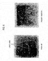
- Fig. 6 shows typical microfocused transmission X-ray pictures comparing the high-temperature solder (AuGe) bonded semiconductor device manufactured in the embodiment and a high-temperature solder bonded semiconductor device obtained in the first prior art (method using no weight).
- the dimensions of the SiC chips appearing as square objects in the pictures are 2 ⁇ 2 mm 2 .
- Portions appearing relatively white in the pictures in terms of contrast are voids existing in high-temperature solder layers.
- an area occupied by the voids is reduced by one tenth or lower compared to the high-temperature solder bonded semiconductor device based on the first prior art.
- the percentage of area occupied by the voids is 5% at maximum and is typically less than 2% (right picture of Fig. 6 ).
- the semiconductor device with no void at all can be also obtained at a high rate. This result is the same for other embodiments described below.
- the high-temperature solder bonded semiconductor device and the method for manufacturing the same of the present invention solve the problem of the first prior art, specifically "void tends to be formed in the high-temperature solder layer".
- the high-temperature solder bonded semiconductor device and the method for manufacturing the same of the present invention solve the problem of the second prior art, specifically "since the power semiconductor device is thermally damaged in the solder bonding process and this causes many defects and deterioration in reliability, the power semiconductor device cannot be practically used".
- the highly-reliable high-temperature solder bonded power semiconductor device with reduced voids can be provided in a high yield.
- the reflow temperature in solder bonding is empirically set to about 50°C above the melting point (or the solidus temperature) in consideration of manufacturing.
- the reflow temperature is 406°C, in the case of AuSi, 413°C, and in the case of ZnAl solder, 430°C.
- the thermal resistance of the current SiC power chip, which is formed by a Si semiconductor fabrication technique, in fabrication is such a level that the SiC power chip can withstand heat of 420°C for several tens of minutes.
- the inventors of the present invention who noticed that there is almost no margin between the recommended reflow temperature for the high-temperature solder and the heatproof temperature of the power chip, focused on temperature history of the second prior art and obtained the following important finding based on an experiment.
- the SiC power chip is configured to directly come into contact with the metal weight with large heat capacity. Accordingly, it is difficult to raise the temperature and, if the temperature is raised to reach a predetermined temperature in a short time, the temperature at the position of the SiC power chip overshoots and exceeds the heatproof temperature, thereby causing damage or severe deterioration of the SiC power chip. If the temperature is made to rise in a long time to alleviate this problem, no overshooting occurs.
- the SiC power chip is kept near the predetermined reflow temperature for a very long time, and the chip is thermally damaged also in this case. Another reason why thermal damage occurs is that the metal weight once heated to a high temperature becomes a heat supply source in a cooling step after the reflow, and temperature fall of the SiC power chip is hindered.
- a configuration is such that the load of the metal weight 16 is applied to the SiC power chip 13 via the heat insulating body 17. Accordingly, the SiC power chip 13 and the metal weight 16 are thermally insulated from each other, and the metal weight 16 is not heated to a high temperature in the reflow process. Hence, the temperature can be rapidly raised and rapidly lowered under a condition where no temperature overshooting occurs. Moreover, it is possible to eliminate the risk of the SiC power chip being kept near the reflow temperature for a long time.
- the high-temperature solder bonded semiconductor device and the method for manufacturing the same of the present invention have thus succeeded in solving the serious problem of the second prior art, specifically "the power semiconductor device is thermally damaged in the solder bonding process and this causes many defects".
- the heat insulating load jig of the embodiment includes the connection columns 20a, 20b, ... detachably connecting the chip alignment plate 18 and the weight supporting plate 19 to each other, the chip alignment plate 18 and the weight supporting plate 19 can be connected and fixed to each other in the predetermined positional relationship.
- connection columns 20a, 20b, ... are fixed to the chip alignment plate 18 or the weight supporting plate 19, operability in attachment can be improved.
- the heat insulating body 17 has the thin shaft structure in at least one portion of the heat transmission route extending from the SiC power chip 13 to the metal weight 16. Accordingly, the heat insulating effect between the SiC power chip 13 and the metal weight 16 can be further improved.
- the heat insulating body 17 has the porous structure, the heat insulating effect between the SiC power chip 13 and the metal weight 16 can be improved.
- the heat insulating body 17 has a coarse structure in at least one of the contact surfaces with the SiC power chip 13 and the metal weight 16, the heat insulating effect between the SiC power chip 13 and the metal weight 16 can be improved.
- the mass of the metal weight 16 is set such that pressure of 0.1 g/cm 2 or more is generated at the solder bonding surface of the SiC power chip 13, voids can be effectively reduced.
- the mass of the metal weight 16 is set such that pressure of 0.3 g/cm 2 or more is generated at the solder bonding surface of the SiC power chip 13, voids can be more effectively reduced.
- the second embodiment of the present invention is described. Since the second embodiment is an invention related to a modification of the heat insulating load jig 11 of the first embodiment, only the description related to the heat insulating load jig is given and description of other parts is omitted.
- Fig. 7 shows a cross-section of a main portion of a heat insulating load jig 31 of the second embodiment.
- Constitutional elements same as those in Fig. 2 are denoted by the same reference numerals as Fig. 2 , and description thereof is omitted to avoid overlapping description.
- Reference numeral 39 denotes a weight supporting plate
- 37 denotes a bar-shaped heat insulating body
- 36 denotes a metal weight.
- the heat insulating body 37 is longer than that in the first embodiment, and an end of a surface coming into contact with the SiC power chip 13 is curved to have a conical shape.
- the heat insulating body 37 protrudes upward from an opening portion of the weight supporting plate 39 and is inserted into a hole provided in a bottom portion of the metal weight 36.
- the heat insulating body 37 has a role of transmitting load to the SiC power chip 13 and blocking heat exchange between the SiC power chip 13 and the metal weight 36.
- the heat insulating body 37 is fixed to the metal weight 36 to facilitate attachment and detachment of the heat insulating load jig 31.
- the method for fixing the heat insulating body 37 is simple. For example, a small screw hole is formed in a lower surface of the metal weight 36, and the heat insulating body 37 is fixed by a set screw.
- the heat insulating body 37 and the metal weight 36 are integrated and used as a heat insulator load 70. This can improve operability in attachment.
- the weight supporting plate 39 is made of a material with small heat capacity (such as graphite or alumina) and has a function of determining a placement position of the metal weight 36 and a function of maintaining a vertical posture of the metal weight 36 in bonding processing. To achieve these functions, the weight supporting plate 39 is provided with a weight through hole through which only the heat insulating body 37 passes and insertion holes for fixing the connection columns 20a, 20b, ... at predetermined positions. In order to improve operability in attachment, it is desirable to fixedly connect the weight supporting plate 39 and the connection columns 20a, 20b, ... and detachably connect the chip alignment plate 18 and the connection columns 20a, 20b, ..., or vice versa. In the embodiment, the case where the weight supporting plate 39 and the connection columns 20a, 20b, ... are integrated together is described below for the convenience of description.
- the embodiment since the heat insulating body 37 is long and narrow and the surface of the heat insulating body 37 coming into contact with the SiC power chip 13 is processed in the conical shape, the heat insulating property is further improved compared to the heat insulating body 17 of the first embodiment. Accordingly, the embodiment can have a higher effect of solving the problem of the second prior art, specifically "since the power semiconductor device is thermally damaged in the solder bonding process and this causes many defects and deterioration in reliability, the power semiconductor device cannot be practically used".
- the SiN substrate 12 is placed on the susceptor 5 (S302), and the chip alignment plate 18 is placed on the SiN substrate 12 while being aligned therewith (S303). Thereafter, the AuGe eutectic solder sheet 14 and the SiC power chip 13 are sequentially dropped into the opening portion provided in the chip alignment plate 18 (S304).
- step S305 the weight supporting plate 39 to which the connection columns 20a, 20b, ... are fixed is placed on the chip alignment plate 18 while being aligned therewith.
- step S306 the heat insulator load 70 obtained by integrating the heat insulating body 37 and the metal weight 36 is inserted into the weight through hole of the weight supporting plate 39.
- the set-up of the heat insulating load jig 31 is thus completed as shown in Fig. 7 .
- the method for manufacturing the SiC semiconductor device of the present invention is finished and the SiC semiconductor device based on the present invention is completed.
- the second embodiment of the present invention can exert such an excellent effect that, in the fabrication process, attachment and detachment of the heat insulating load jig can be performed more easily than in the first embodiment.
- the heat insulating load jigs of the first and second embodiments are configured such that the metal load which is heavy in weight protrudes outward above the chip alignment plate, the weight supporting plate, and the connection columns which are relatively light in weight. Accordingly, the center of gravity is high and, in a case where the weight of the metal weight is heavy or a case where multiple metal weights are attached for one SiN substrate, great care is needed to be taken not to tip over the heat insulating load jig and the SiN substrate 12.
- an object of the third embodiment is to solve such a problem of the heat insulating load jigs of the first and second embodiments and improve productivity.
- Fig. 9 shows a cross section of a main portion of a heat insulating load jig 41 based on the third embodiment.
- the embodiment is described as a case where the heat insulating load jig 31 of the second embodiment ( Fig. 7 ) is modified to stabilize the center of gravity.
- the embodiment can be similarly applied to the heat insulating load jig 11 of the first embodiment.
- Constitutional elements same as those in Fig. 7 are denoted by the same reference numerals as Fig. 7 , and description thereof is omitted to avoid overlapping description.
- reference numeral 42 denotes a center-of-gravity stabilizing frame placed on the susceptor 5, and the center-of-gravity stabilizing frame 42 has a shape like "a box without top and bottom surfaces".
- An inner wall of the center-of-gravity stabilizing frame 42 comes into contact with any one of a set of the SiN substrate 12 and the weight supporting plate 39, a set of the chip alignment plate 18 and the weight supporting plate 39, and a set of the SiN substrate 12, the chip alignment plate 18, and the weight supporting plate 39 with a small clearance provided
- the center-of-gravity stabilizing frame 42 is illustrated as a simple frame in Fig. 9 , an effect of further stabilizing the center of gravity can be obtained by forming the center-of-gravity stabilizing frame 42 to have a L-shaped cross section extending toward an outer periphery.
- step S405 the center-of-gravity stabilizing frame 42 is placed on a peripheral portion of the chip alignment plate 18 and the SiN substrate 12.
- step S406 the weight supporting plate 39 is gently dropped into the center-of-gravity stabilizing frame 42, the weight supporting plate 39 being assembled such that the connection columns 20a, 20b, ... are fixed thereto and the metal weight 36 (heat insulator load) to which the heat insulating body 37 is attached is inserted into the through hole of the weight supporting plate 39.
- the set-up of the heat insulating load jig is thus completed as shown in Fig. 9 .
- the method for manufacturing the SiC semiconductor device of the present invention is finished and the SiC semiconductor device based on the present invention is completed.
- the third embodiment since the third embodiment includes all of the configurations of the first and second embodiments, the third embodiment can exert all of the effects obtained in the first and second embodiments. Furthermore, since the heat insulating load jig 41 is configured to include the center-of-gravity stabilizing frame 42, a risk of the heat insulating load jig 41 tipping over can be reduced. Hence, it is possible to increase the speed of the conveyor or the speed of the arm of the robot in the mass production apparatus employing the mode in which the susceptor 5 moves like a conveyor or the mass production apparatus configured to place the heat insulating load jig with the robot, and improve productivity.
- the embodiments described above are not limited to bonding of one power chip and can be applied to a case of bonding multiple chips as a matter of course.
- description is given of a case where the third embodiment is applied to bonding of multiple chips.
- the heat insulating load jig is modified to improve productivity. Since the fourth embodiment is the same as the aforementioned embodiments except for the configuration of the heat insulating load jig and the method for setting up the heat insulating load jig, overlapping description is omitted.
- Fig. 11 is a cross-sectional diagram of a main portion of a heat insulating load jig 45 of the fourth embodiment and is an assembly diagram showing a state where the heat insulating load jig 45 is attached above the SiN substrate 12 and the SiC power chip 13.
- Constitutional parts denoted by the same reference numerals as those in the first to third embodiments are the same parts as those in these embodiments, and description thereof is omitted to avoid overlapping description.
- reference numeral 46 denotes a chip alignment plate.
- the chip alignment plate 46 is significantly different from the chip alignment plate 18 in the first to third embodiment in that an upper portion of each of chip through holes for placing power chips has a tapered shape (slope) inclined to become wider toward the upper side. Due to this tapered shape, the AuGe solder and the SiC power chip slide down the taper and are automatically arranged at an exact position. In other words, this tapered shape has such an effect that positional accuracy required for placement of the AuGe solder and the SiC power chip is greatly relaxed and productivity in chip placement can be improved.
- reference numeral 47 denotes a weight supporting plate.
- the weight supporting plate 47 has the same basic functions as the weight supporting plate 39 in the first to third embodiments but is different in that the weight supporting plate 47 includes opening portion sheaths 48 respectively for weight through holes through which the heat insulating bodies 37 (or the metal weights 36) pass.
- the opening portion sheaths 48 have functions of preventing the heat insulating bodies 37 and the metal weights 36 from tipping over and maintaining the postures of the heat insulating bodies 37 and the metal weights 36 in a substantially vertical state. In a case where there are many metal weights 36 as shown in Fig.
- reference numeral 49 denotes first connection columns
- 50 denotes second connection columns.
- the first connection columns 49 are configured to be fixed to the weight supporting plate 47 and come into contact with a surface of the chip alignment plate 46. Since a purpose of the first connection columns 49 is to support the weight supporting plate 47, at least three, desirably four or more first connection columns 49 are preferably provided.
- the second connection columns 50 are fixed to the chip alignment plate 46 and can be easily inserted into opening portions penetrating predetermined portions of the weight supporting plate 47 with a certain clearance provided.
- the function of the second connection columns 50 is to quickly and accurately align the weight supporting plate 47 with the chip alignment plate 46. Since a work time required for the alignment becomes longer as the number of the second connection columns 50 becomes greater (this is because the number of portions to be inserted and fitted becomes greater), the number of the second connection columns 50 provided is desirably the smallest possible number equal to or greater than two.
- connection columns are divided into two types of the first connection column and the second connection column.
- configuration may such that connection columns are not divided into various types as described in the first to third embodiments.
- Contaminants are first removed, the SiN substrate 12 is placed on the susceptor 5 (omitted in the drawing), and the chip alignment plate 46 to which the second columns 50 are attached is then placed on the SiN substrate 12 while being aligned therewith. Thereafter, the AuGe eutectic solder sheet 14 and the SiC power chip 13 are placed by being sequentially dropped into each of the chip through holes provided in the chip alignment plate 46, the AuGe eutectic solder sheets 14 and the SiC power chips 13 being provided as many as the opening portions of the chip alignment plate 46.
- center-of-gravity stabilizing frame 42 is placed around the outer peripheries of the chip alignment plate 46 and the SiN substrate 12.
- the first connection columns 49 are attached, and the weight supporting plate 47 assembly having through holes into which the multiple heat insulating bodies 37 (with the metal weights 36) are inserted is gently dropped into the center-of-gravity stabilizing frame 42.
- the set-up of the heat insulating load jig is thus completed.
- the method for manufacturing the SiC semiconductor device of the present invention is finished and the SiC semiconductor device of the present invention is completed.
- the heat insulating load jig of the embodiment can bond multiple SiC power chips and improve productivity.
- each of the chip through holes of the chip alignment plate 46 has the tapered structure inclined to become wider toward the upper side, it is possible to greatly relax the positional accuracy required for the placement of the AuGe solder and the SiC power chip and improve productivity in chip placement.
- the sheath structures having the same cross section as the weight through holes of the weight supporting plate 47 are attached to the weight through holes. Accordingly, the risk of the heat insulating load jig 45 tipping over can be greatly reduced.
- the aforementioned heat insulating load jigs of the first to fourth embodiments are configured such that the weight supporting plate is placed on the chip alignment plate via the connection columns.
- the heat insulating load jig can be configured without using the connection columns.
- a heat insulating load jig having such a configuration is provided.
- Fig. 12 is a cross-sectional diagram of a main portion of a heat insulating load jig 60 of the fifth embodiment.
- Constitutional parts denoted by the same reference numerals as those in the aforementioned embodiments are the same members, and description thereof is omitted to avoid overlapping description.
- reference numeral 61 denotes a weight supporting plate
- 62 denotes a center-of-gravity stabilizing frame
- the functions and material of the weight supporting plate 61 are completely the same as the weight supporting plate 39 in the aforementioned embodiments.
- the weight supporting plate 61 is supported not by the connection columns but by the center-of-gravity stabilizing frame 62.
- the positioning of the weight supporting plate 61 relative to the SiN substrate 12 is also performed by using the center-of-gravity stabilizing frame 62.
- step S505 the center-of-gravity stabilizing frame 62 is placed on peripheries of the chip alignment plate 18 and the SiN substrate 12.
- step S506 the weight supporting plate 61 is placed by being gently dropped into a recess portion of the center-of-gravity stabilizing frame 62.
- step S507 the metal weight 36 to which the heat insulating body 37 is fixed is inserted into the weight supporting plate 61. The set-up of the heat insulating load jig 60 is thus completed as shown in Fig. 12 .
- the method for manufacturing the SiC semiconductor device of the present invention is finished and the SiC semiconductor device of the present invention is completed.
- the heat insulating load jig of the fifth embodiment includes all of the functions of the third embodiment, the heat insulating load jig can exert all of the effects obtained in the third embodiment. Moreover, in the embodiment, since the heat insulating load jig is configured to include no connection columns, there is obtained such a unique effect that the heat insulating load jig can be fabricated at a lower cost than in the first to fourth embodiments.
- the method for manufacturing the semiconductor device, the heat insulating load jig, and the method for setting up the heat insulating load jig of one embodiment of the present invention load is applied to the semiconductor device from above via the heat insulating body. Accordingly, the semiconductor device and the load are thermally insulated from each other, and it is possible to achieve rapid heating, melting of the solder in a short time, and rapid cooling. This can not only reduce voids but also avoid excessive temperature rise and long-time heat treatment and practically eliminate thermal damage to the semiconductor device. As a result, a highly-reliable power semiconductor device bonded by using high-temperature solder with few voids can be obtained in a high yield. Accordingly, the method for manufacturing the semiconductor device, the heat insulating load jig, and the method for setting up the heat insulating load jig of one embodiment of the present invention are useful in industries.
Landscapes
- Engineering & Computer Science (AREA)
- Manufacturing & Machinery (AREA)
- Microelectronics & Electronic Packaging (AREA)
- Physics & Mathematics (AREA)
- Optics & Photonics (AREA)
- Mechanical Engineering (AREA)
- Die Bonding (AREA)
- Supply And Installment Of Electrical Components (AREA)
- Cooling Or The Like Of Semiconductors Or Solid State Devices (AREA)
Abstract
Description
- The present invention relates to a method for manufacturing a semiconductor device formed by bonding a semiconductor element and a substrate with a high-temperature solder bonding material, a heat insulating load jig used in bonding of the high-temperature solder material, and a method for setting up the heat insulating load jig.
- Power semiconductor devices using wide-bandgap semiconductor such as silicon carbide (SiC), gallium nitride (GaN), and diamond (C) have lower on-resistance than those of conventional semiconductor devices using silicon (Si) and gallium arsenide (GaAs), and can perform high-voltage and high-current operations at a high semiconductor junction temperature (Tj). Accordingly, reduction of the area of the semiconductor device and drastic simplification of a cooler is achieved at the same time, and it is expected that a small, light-weight, low-cost power electronic system can be achieved.
- A bonding portion (so-called die bond using solder) with an electrically-conductive substrate in such a power semiconductor device requires high heat resistance as a matter of course. In view of this, AuGe eutectic solder (melting point 356°C), AuSi eutectic solder (melting point 363°C), ZnAl eutectic solder (melting point 380°C), and the like which have high melting points are considered to be used as solder materials in such a power semiconductor device (Non-patent Literatures 1 to 3 and Patent Literature 1).
- However, when the bonding portion of the semiconductor device is formed by using the high-temperature solder materials described above, voids tend to be formed in a high-temperature solder layer as clearly shown in
Fig. 6 of Non-patent Literature 1 andFig. 8a ofPatent Literature 2, and reduction of these voids is a major development problem (first prior art). - A known method for suppressing formation of voids in the die bond solder is a method in which a metal weight is placed on the semiconductor device and the semiconductor device is heated in this state to reflow the solder. Fig. 22 of
Non-patent Literature 3 can be given as a specific example of the most sophisticated solder jig (second prior art). - Patent Literature 1: Japanese Patent Application Publication No.
2009-125753 -
- Non-patent Literature 1: S. Tanimoto el al, Proceedings of IMAPS HiTEC 2010 (May 11-13, 2010, Albuquerque, New Mexico, USA), pp. 32-39.
- Non-patent Literature 2: Y. Yamada el al, Microelectronics Reliability Vol. 47 (2007) pp. 2147-2151.
- Non-patent Literature 3: Michael J. Palmer al, Proceedings of IMAPS HiTEC 2010 (May 11-13, 2010, Albuquerque, New Mexico, USA), pp. 316-324.
- If the power semiconductor device and the substrate are bonded to each other with the high-temperature solder by using the aforementioned second prior art, although the voids can be reduced, the power semiconductor device is thermally damaged and this causes many defects and deterioration in reliability. Accordingly, the second prior art has a problem that the power semiconductor device cannot be practically used. Defect modes (or deterioration in reliability) in this case include short circuit between a gate and a source (a base and an emitter), defective insulation, deterioration in the withstanding voltage of a gate insulating film, and the like.
- The present invention is proposed in view of the circumstances described above, and a first object of the present invention is to provide a high-temperature solder void reduction technique which causes no thermal damage. Moreover, a second object of the present invention is to achieve a high-temperature solder die bond and a power semiconductor device in which voids are reduced by using this improved technique.
- In the present invention, a circuit board and a semiconductor chip are bonded to each other by: interposing a solder material between the circuit board and the semiconductor chip, the solder material having a melting point or a solidus temperature in a range between a heatproof temperature of the semiconductor chip and a temperature 100°C below the heatproof temperature; and melting and solidifying the solder material with load applied to the semiconductor chip from above via a heat insulating body. The present invention can thereby achieve the two objects described above.
-
- [
Fig. 1] Fig. 1 is a block diagram showing a configuration of a reflow equipment in which a heat insulating load jig of the present invention is used. - [
Fig. 2] Fig. 2 is a cross-sectional diagram showing a structure of a heat insulating load jig in a first embodiment of the present invention. - [
Fig. 3] Fig. 3 is a diagram showing a structure of a heat insulating body in a heat insulating load jig of the present invention. - [
Fig. 4] Fig. 4 is a flowchart showing procedures of a method for setting up the heat insulating load jig in the first embodiment of the present invention. - [
Fig. 5] Fig. 5 is a flowchart showing procedures of a reflow process using the heat insulating load jig of the present invention. - [
Fig. 6] Fig. 6 is a diagram for explaining effects obtained by a method for manufacturing a semiconductor device which uses the heat insulating load jig of the present invention. - [
Fig. 7] Fig. 7 is a cross-sectional diagram showing a structure of a heat insulating load jig in a second embodiment of the present invention. - [
Fig. 8] Fig. 8 is a flowchart showing procedures of a method for setting up the heat insulating load jig in the second embodiment of the present invention. - [
Fig. 9] Fig. 9 is a cross-sectional diagram showing a structure of a heat insulating load jig in a third embodiment of the present invention. - [
Fig. 10] Fig. 10 is a flowchart showing procedures of a method for setting up the heat insulating load jig in the third embodiment of the present invention. - [
Fig. 11] Fig. 11 is a cross-sectional diagram showing a structure of a heat insulating load jig in a fourth embodiment of the present invention. - [
Fig. 12] Fig. 12 is a cross-sectional diagram showing a structure of a heat insulating load jig in a fifth embodiment of the present invention. - [
Fig. 13] Fig. 13 is a flowchart showing procedures of a method for setting up the heat insulating load jig in the fifth embodiment of the present invention. - First to fifth embodiments to which the present invention is applied are described below with reference to the drawings.
- The first embodiment of a method for manufacturing a semiconductor device which uses a heat insulating load jig of the present invention is described with reference to
Figs. 1 to 4 . Note that these drawings are schematically illustrated to facilitate the understanding of the present invention, and relationships between thicknesses and plan dimensions, ratios of thicknesses between layers, and the like are illustrated in an exaggerated manner. - Moreover, the first embodiment is described below by giving an example in which a SiC power chip is used as a semiconductor device, a circuit board (hereafter, simply referred to as board in some cases) in which Cu plates are attached as circuit electrical conductors on both surfaces of a SiN ceramic plate is used as a circuit board, and AuGe eutectic solder is used as high-temperature solder. However, this is merely an example, and the present invention can be equally applied to cases where other wide-bandgap semiconductor elements such as a GaN element, a diamond element, and a ZnO element, as well as Si semiconductor elements for high temperature usage (a power element, a SOI element, and a sensor element) are used as the semiconductor power device. Moreover, the circuit conductors are not limited to the Cu plates attached to the SiN ceramic plate and may be Cu-based material attached to a different type of ceramic substrate or metal plates (Al, CuMo, or the like) other than the Cu plates attached to a different type of ceramic substrate (Al2O3, AlN, or the like) or an insulating body. Alternatively, the circuit conductors may be Cu plates or simple metal plates made of an elemental metal (without the ceramic plate or the insulating plate) other than Cu (in this case, the metal plate itself is the circuit board). Moreover, the high-temperature solder can be defined as solder having a melting point or a solidus temperature in a range between a heatproof temperature of the used semiconductor device and a temperature 100°C below the heatproof temperature, and may be Au-Si, Zn-Al, or other materials.
- An overall configuration of a high-temperature solder bond forming apparatus used in the present invention is described.
-
Fig. 1 is a schematic cross-sectional diagram of a main portion of a bonding apparatus in which the heat insulating load jig of the present invention is used. Reference numeral 1 denotes a general-purpose reflow equipment, and the reflow equipment 1 includes sealedchambers exhaust device 3 configured to reduce the pressure inside the chamber, and agas supplying device 4 configured to deliver an inert gas (Ar or N2) with low dew point into the chamber. A horizontally-placedsusceptor 5 made of carbon or Al and alamp heater 6 capable of rapidly heating thesusceptor 5 are placed inside the chamber. The atmosphere inside the chamber and the temperature of thesusceptor 5 are controlled by aprogram control device 7. - A
bonding sample 10 is placed on thesusceptor 5, and a heatinsulating load jig 11 configured to apply load to the bondingsample 10 in a thermally-insulated manner is placed on thebonding sample 10. -
Fig. 2 is a detailed diagram of thebonding sample 10 and the heatinsulating load jig 11 and shows a state before bonding. - The
bonding sample 10 is formed of a SiN (silicon nitride)substrate 12 placed to come into contact with thesusceptor 5, aSiC power chip 13, an AuGe eutectic solder sheet (or paste) 14 held between theSiN substrate 12 and theSiC power chip 13.Cu circuit plates SiN substrate 12 by using silver solder or the like (not illustrated). Surfaces of theCu circuit plates Cu circuit plates SiC power chip 13 is coated with metallization (not illustrated) for normal solder such as Ti/Ni/Ag. - Meanwhile, the heat
insulating load jig 11 is formed at least of ametal weight 16 made of metal and having a pillar shape (circular column shape or prismatic column shape) and aheat insulating body 17 disposed between themetal weight 16 and theSiC power chip 13. Achip alignment plate 18, aweight supporting plate 19, andconnection columns - A metal weight (metal load means) 16 acts as a source of load applied to the
SiC power chip 13, like the metal weight in the prior art. Load equal to that in the prior art can be applied to theSiC power chip 13 via theheat insulating body 17. The shape of themetal weight 16 is preferably a circular column or a polygonal column which are such shapes that a dynamic balance can be easily achieved, but is not limited to these shapes. The weight of themetal weight 16 is determined such that chip load (pressure) is at least 0.1 g/cm2 or more, preferably 0.3 g/cm2 or more. - The heat insulating body (heat insulating means) 17 has a function of blocking (to be precise, strongly suppressing) heat conduction between the
SiC power chip 13 and themetal weight 16. Specifically, theheat insulating body 17 blocks transfer of heat from theSiC power chip 13 to themetal weight 16 when the temperature of theSiC power chip 13 is high and blocks transfer of heat in a reverse direction when the temperature of themetal weight 16 is high. Such heat insulating function of theheat insulating body 17 allows theSiC power chip 13 to be rapidly heated and rapidly cooled along with change in the temperature of thesusceptor 5, without being thermally affected by themetal weight 16 whose heat capacity is very large. The material of theheat insulating body 17 is preferably alumina or an insulating body (for example, steatite porcelain, borosilicate glass, or the like) which has a lower thermal conductivity than alumina and which can sufficiently withstand the reflow temperature. The shape of theheat insulating body 17 may be a simple pellet of a flat circular-column shape or a flat polygonal-column shape as shown inFig. 2 as an example. However, it is preferable that theheat insulating body 17 has a shape which limits the heat conduction between theSiC power chip 13 and themetal weight 16 to further improve the heat insulating effect. As such a structure, theheat insulating body 17 has a thin shaft structure in at least one portion of a heat transmission route extending from theSiC power chip 13 to themetal weight 16. Examples of such a structure include a conical shape (circular conical shape and polygonal pyramid shape), an inverted conical shape, a thumbtack shape (inverted and upright), a needle shape, and the like as shown inFig. 3 . Note that tips of the inverted conical shape, the inverted thumbtack shape, and the inverted needle shape are formed to be round to have R of about 100 µm so as not to damage surface electrodes of theSiC power chip 13. Moreover, making the structure of theheat insulating body 17 porous (like pumice) is also very effective. Furthermore, making contact surfaces of theheat insulating body 17 withSiC power chip 13 and themetal weight 16 coarse is also considerably effective. - The
heat insulating body 17 and themetal weight 16 may be integrated as a heat insulator load (heat insulating load means). - The chip alignment plate (chip alignment means) 18 (
Fig. 2 ) has a function of alignment with theSiN substrate 12, and has a chip through hole for arranging the solder sheet and the SiC power chip at a predetermined position of theSiN substrate 12. Thechip alignment plate 18 is made of a material with small heat capacity such as graphite or alumina and mainly functions as a template for arranging theSiC power chip 13 at the predetermined position of theSiN substrate 12. Thechip alignment plate 18 is positioned by uniquely fitting theSiN substrate 12 to a recess portion carved on a bottom surface of thechip alignment plate 18. The chip through hole is opened at a position where theSiC power chip 13 is to be disposed (a position on theCu circuit plate 15a in any cases), and is slightly larger than theSiC power chip 13. - The weight supporting plate (weight supporting means) 19 is arranged above and away from the
chip alignment plate 18 by a predetermined distance. Theweight supporting plate 19 has a function of alignment with thechip alignment plate 18 or theSiN substrate 12, and has a weight through hole at a position corresponding to the position of the chip through hole. Like thechip alignment plate 18, theweight supporting plate 19 is also made of a material with small heat capacity (graphite, alumina, or the like) and has a function of determining a position where themetal weight 16 is to be placed and a function of preventing tip-over of themetal weight 16 in bonding processing. - The
connection columns chip alignment plate 18 and theweight supporting plate 19 to each other in a predetermined positional relationship. To achieve this function, insertion holes into which the connection columns can be inserted without a gap are provided at predetermined positions in theweight supporting plate 19 and thechip alignment plate 18. In order to improve operability in attachment of the heat insulatingload jig 11, it is desirable to fixedly connect theweight supporting plate 19 and theconnection columns chip alignment plate 18 and theconnection columns - Next, a method for setting up the heat insulating load jig used in the aforementioned high-temperature solder bonding apparatus is described with reference to
Fig. 4 . - First, in step S101, required numbers of the
SiC power chips 13 and the SiN (silicon nitride)substrates 12 are prepared and are cleaned by using organic solution such as acetone or isopropyl alcohol to remove contaminants adhering to surfaces of these precursor materials. Here, the SiC power chips 13 are SiC power semiconductor elements desired to be used together, and there are prepared power chips such as MOSFET, JFET, and BJT, power chips such as a Schottky diode and a pn diode, and the like which are required. - Next, in step S102, the
chamber 2a of the reflow equipment 1 ofFig. 1 is opened to place theSiN substrate 12 on the susceptor 5 (Fig. 2 ). Then, in step S103, thechip alignment plate 18 is placed on theSiN substrate 12 while being aligned therewith. After thechip alignment plate 18 is placed, next, in step S104, the AuGeeutectic solder sheet 14 and theSiC power chip 13 are placed by being sequentially dropped into the chip through hole which is an opening portion provided in thechip alignment plate 18. Then, in step S105, theheat insulating body 17 is placed on theSiC power chip 13. In this case, theSiC power chip 13 is placed such that the bonding surface (back surface) thereof comes into contact with the AuGeeutectic solder sheet 14, as a matter of course. In a case where theheat insulating body 17 and themetal weight 16 are integrated with each other, theheat insulating body 17 is placed together with themetal weight 16 at the time when themetal weight 16 is placed later. - Next, in step S106, the
weight supporting plate 19 to which theconnection columns chip alignment plate 18. This attachment is executed by correctly inserting theconnection columns chip alignment plate 18. - Lastly, in S107, the
metal weight 16 is placed on theheat insulating body 17 through the weight through hole of theweight supporting plate 19, and the set-up of the heat insulatingload jig 11 is thus finished. - Next, after the aforementioned set-up of the heat insulating
load jig 11 is completed, thechamber 2a of the reflow equipment 1 ofFig. 1 is closed to execute the reflow process. - Processing in the reflow process is described below with reference to
Fig. 5 . Note that temperature control, gas delivery control, and exhaust control in the reflow process are performed based on instructions from the aforementionedprogram control device 7. - First, in step S201, the
exhaust device 3 of the reflow equipment 1 is activated to exhaust air inside thechambers chambers gas supplying device 4. This operation is performed several times to replace the air inside the sample chamber with the inert gas. - After the replacement with the inert gas is completed, preheating is subsequently performed in step S202. The
lamp heater 6 is powered up to heat thesusceptor 5, and the temperature of theSiN substrate 12 and theSiC power chip 13 is raised to about 200°C. This temperature is maintained for about two minutes. In this case, removal of organic contaminations may be promoted by introducing an inert gas including formic acid vapor. - Then, in step S203, the introduction of the inert gas is stopped, and the
exhaust device 3 is activated to exhaust air inside thechambers chambers lamp heater 6 is increased to further heat thesusceptor 5, and the temperature of theSiN substrate 12 and theSiC power chip 13 is raised to and maintained at a predetermined temperature in a temperature range between the solidus temperature of the high-temperature solder (in the case of AuGe, 356°C = melting point) and the maximum temperature of 420°C. The time maintained at the predetermined temperature is five minutes at the longest. For example, in the case where the AuGe solder is used and the predetermined temperature is set to 400°C, the time maintained at the predetermined temperature is typically one minute. When the temperature exceeds the melting point (356°C), the AuGe solder turns into melt and is crushed by the load of the heat insulatingload jig 11. In this case, air bubbles formed by remaining gas and the like are moved outside the solder layer and minimized due to combination of an effect of the reduced pressure and an effect of the high temperature. - Next, in step S204, the inert gas is introduced into the
chambers susceptor 5, theSiN substrate 12, and theSiC power chip 13 is immediately started. In this short time after the introduction of the inert gas, the air bubbles remaining in the AuGe solder melt become extremely small due to an increase of external pressure and a rapid decrease of the temperature, and the AuGe solder melt solidifies in this state. Accordingly, an AuGe bonding layer with few voids formed due to air bubbles can be formed. - Moreover, since the
SiC power chip 13 is in contact with themetal weight 16 with high heat capacity with theheat insulating body 17 provided therebetween, it is possible to cool theSiC power chip 13 more rapidly than in the prior arts, and reduce voids formed due to solid layer alloy reaction (Kirkendall reaction) between the AuGe solder layer and each of the solder metallization of theSiC power chip 13 and the plating layer of the Cu-SiN substrateCu circuit plate 15a. - After the
susceptor 5, theSiN substrate 12, and theSiC power chip 13 are cooled down to a room temperature, in step S205, thechamber 2a is opened, the heat insulatingload jig 11 is removed, and the bonding sample 10 (= SiC power chip/SiN substrate bonded body) is taken out. A high-temperature solder bonded semiconductor device is thus completed, and the reflow process of the embodiment is finished. - As described above in detail, since the heat insulating load jig of the embodiment is configured to apply load to the semiconductor device from above via the heat insulating body, the semiconductor device and the load are thermally insulated from each other, and it is possible to achieve rapid heating, melting of the solder in a short time, and rapid cooling. This can not only reduce voids but also avoid excessive temperature rise and long-time heat treatment and practically eliminate thermal damage to the semiconductor device. As a result, a highly-reliable power semiconductor device bonded by using high-temperature solder with few voids can be obtained in a high yield.
- Effects of the heat insulating load jig of the embodiment are described below in detail with reference to
Fig. 6. Fig. 6 shows typical microfocused transmission X-ray pictures comparing the high-temperature solder (AuGe) bonded semiconductor device manufactured in the embodiment and a high-temperature solder bonded semiconductor device obtained in the first prior art (method using no weight). The dimensions of the SiC chips appearing as square objects in the pictures are 2×2 mm2. Portions appearing relatively white in the pictures in terms of contrast are voids existing in high-temperature solder layers. - Comparing these pictures, difference is apparent. According to the high-temperature solder bonded semiconductor device and the method for manufacturing the same of the embodiment, an area occupied by the voids is reduced by one tenth or lower compared to the high-temperature solder bonded semiconductor device based on the first prior art. In the embodiment, the percentage of area occupied by the voids is 5% at maximum and is typically less than 2% (right picture of
Fig. 6 ). The semiconductor device with no void at all can be also obtained at a high rate. This result is the same for other embodiments described below. - From the facts described above, it can be said that the high-temperature solder bonded semiconductor device and the method for manufacturing the same of the present invention solve the problem of the first prior art, specifically "void tends to be formed in the high-temperature solder layer".
- Thirty high-temperature solder (AuGe) bonded semiconductor devices based on the present invention and another thirty devices based on the second prior art were manufactured under a condition where the formation of voids was reduced. In a characteristic test, the semiconductor devices based on the present invention were all good products. Meanwhile, 21 semiconductor devices based on the second prior art were defective products and nine were good products. Defect modes were insufficient withstanding voltage and short circuit between a gate and a source. Next, the thirty semiconductor devices based on the present invention and the nine good semiconductor devices based on the second prior art were subjected to heat exposure test at 300°C. All of the semiconductor devices based on the second prior art became defective within 100 hours. Meanwhile, all of the semiconductor devices based on the present invention survived the 3000-hour test and no defect occurred.
- From the facts described above, it can be said that the high-temperature solder bonded semiconductor device and the method for manufacturing the same of the present invention solve the problem of the second prior art, specifically "since the power semiconductor device is thermally damaged in the solder bonding process and this causes many defects and deterioration in reliability, the power semiconductor device cannot be practically used".
- As described above, in the high-temperature solder bonded semiconductor device and the method for manufacturing the same of the present invention, the highly-reliable high-temperature solder bonded power semiconductor device with reduced voids can be provided in a high yield.
- Next, description is given of how the high-temperature solder bonded semiconductor device and the method for manufacturing the same of the present invention can prevent defects and deterioration of reliability.
- It is known that the reflow temperature in solder bonding is empirically set to about 50°C above the melting point (or the solidus temperature) in consideration of manufacturing. In the case of AuGe, the reflow temperature is 406°C, in the case of AuSi, 413°C, and in the case of ZnAl solder, 430°C. Meanwhile, the thermal resistance of the current SiC power chip, which is formed by a Si semiconductor fabrication technique, in fabrication is such a level that the SiC power chip can withstand heat of 420°C for several tens of minutes. The inventors of the present invention, who noticed that there is almost no margin between the recommended reflow temperature for the high-temperature solder and the heatproof temperature of the power chip, focused on temperature history of the second prior art and obtained the following important finding based on an experiment.
- In the second prior art, i.e. a high-temperature solder bonding process in a method for manufacturing a semiconductor device described in
Non-patent Literature 3, the SiC power chip is configured to directly come into contact with the metal weight with large heat capacity. Accordingly, it is difficult to raise the temperature and, if the temperature is raised to reach a predetermined temperature in a short time, the temperature at the position of the SiC power chip overshoots and exceeds the heatproof temperature, thereby causing damage or severe deterioration of the SiC power chip. If the temperature is made to rise in a long time to alleviate this problem, no overshooting occurs. However, the SiC power chip is kept near the predetermined reflow temperature for a very long time, and the chip is thermally damaged also in this case. Another reason why thermal damage occurs is that the metal weight once heated to a high temperature becomes a heat supply source in a cooling step after the reflow, and temperature fall of the SiC power chip is hindered. - In view of this, the inventors understanding such mechanism of thermal damage have worked hard to come up with the present invention. Specifically, in the high-temperature solder bonding process in the method for manufacturing the high-temperature solder bonded semiconductor of the present invention, a configuration is such that the load of the
metal weight 16 is applied to theSiC power chip 13 via theheat insulating body 17. Accordingly, theSiC power chip 13 and themetal weight 16 are thermally insulated from each other, and themetal weight 16 is not heated to a high temperature in the reflow process. Hence, the temperature can be rapidly raised and rapidly lowered under a condition where no temperature overshooting occurs. Moreover, it is possible to eliminate the risk of the SiC power chip being kept near the reflow temperature for a long time. The high-temperature solder bonded semiconductor device and the method for manufacturing the same of the present invention have thus succeeded in solving the serious problem of the second prior art, specifically "the power semiconductor device is thermally damaged in the solder bonding process and this causes many defects". - Moreover, since the heat insulating load jig of the embodiment includes the
connection columns chip alignment plate 18 and theweight supporting plate 19 to each other, thechip alignment plate 18 and theweight supporting plate 19 can be connected and fixed to each other in the predetermined positional relationship. - Furthermore, in the heat insulating load jig of the embodiment, since the
connection columns chip alignment plate 18 or theweight supporting plate 19, operability in attachment can be improved. - Moreover, in the heat insulating load jig of the embodiment, the
heat insulating body 17 has the thin shaft structure in at least one portion of the heat transmission route extending from theSiC power chip 13 to themetal weight 16. Accordingly, the heat insulating effect between theSiC power chip 13 and themetal weight 16 can be further improved. - Furthermore, in the heat insulating load jig of the embodiment, since the
heat insulating body 17 has the porous structure, the heat insulating effect between theSiC power chip 13 and themetal weight 16 can be improved. - Moreover, in the heat insulating load jig of the embodiment, since the
heat insulating body 17 has a coarse structure in at least one of the contact surfaces with theSiC power chip 13 and themetal weight 16, the heat insulating effect between theSiC power chip 13 and themetal weight 16 can be improved. - Furthermore, in the heat insulating load jig of the embodiment, since the mass of the
metal weight 16 is set such that pressure of 0.1 g/cm2 or more is generated at the solder bonding surface of theSiC power chip 13, voids can be effectively reduced. - Moreover, in the heat insulating load jig of the embodiment, since the mass of the
metal weight 16 is set such that pressure of 0.3 g/cm2 or more is generated at the solder bonding surface of theSiC power chip 13, voids can be more effectively reduced. - Next, the second embodiment of the present invention is described. Since the second embodiment is an invention related to a modification of the heat insulating
load jig 11 of the first embodiment, only the description related to the heat insulating load jig is given and description of other parts is omitted. -
Fig. 7 shows a cross-section of a main portion of a heat insulatingload jig 31 of the second embodiment. Constitutional elements same as those inFig. 2 are denoted by the same reference numerals asFig. 2 , and description thereof is omitted to avoid overlapping description.Reference numeral 39 denotes a weight supporting plate, 37 denotes a bar-shaped heat insulating body, and 36 denotes a metal weight. - Detailed description is given by focusing on differences with the first embodiment. The
heat insulating body 37 is longer than that in the first embodiment, and an end of a surface coming into contact with theSiC power chip 13 is curved to have a conical shape. Theheat insulating body 37 protrudes upward from an opening portion of theweight supporting plate 39 and is inserted into a hole provided in a bottom portion of themetal weight 36. Theheat insulating body 37 has a role of transmitting load to theSiC power chip 13 and blocking heat exchange between theSiC power chip 13 and themetal weight 36. - Note that, it is preferable that the
heat insulating body 37 is fixed to themetal weight 36 to facilitate attachment and detachment of the heat insulatingload jig 31. The method for fixing theheat insulating body 37 is simple. For example, a small screw hole is formed in a lower surface of themetal weight 36, and theheat insulating body 37 is fixed by a set screw. In the embodiment, theheat insulating body 37 and themetal weight 36 are integrated and used as aheat insulator load 70. This can improve operability in attachment. - The
weight supporting plate 39 is made of a material with small heat capacity (such as graphite or alumina) and has a function of determining a placement position of themetal weight 36 and a function of maintaining a vertical posture of themetal weight 36 in bonding processing. To achieve these functions, theweight supporting plate 39 is provided with a weight through hole through which only theheat insulating body 37 passes and insertion holes for fixing theconnection columns weight supporting plate 39 and theconnection columns chip alignment plate 18 and theconnection columns weight supporting plate 39 and theconnection columns - As is apparent from the aforementioned description of the structure, in the embodiment, since the
heat insulating body 37 is long and narrow and the surface of theheat insulating body 37 coming into contact with theSiC power chip 13 is processed in the conical shape, the heat insulating property is further improved compared to theheat insulating body 17 of the first embodiment. Accordingly, the embodiment can have a higher effect of solving the problem of the second prior art, specifically "since the power semiconductor device is thermally damaged in the solder bonding process and this causes many defects and deterioration in reliability, the power semiconductor device cannot be practically used". - Next, a method for setting up the heat insulating
load jig 31 for high-temperature solder bonding is described with reference toFig. 8 . - As in the first embodiment, after contaminants are removed (S301), the
SiN substrate 12 is placed on the susceptor 5 (S302), and thechip alignment plate 18 is placed on theSiN substrate 12 while being aligned therewith (S303). Thereafter, the AuGeeutectic solder sheet 14 and theSiC power chip 13 are sequentially dropped into the opening portion provided in the chip alignment plate 18 (S304). - Then, in step S305, the
weight supporting plate 39 to which theconnection columns chip alignment plate 18 while being aligned therewith. Then, in step S306, theheat insulator load 70 obtained by integrating theheat insulating body 37 and themetal weight 36 is inserted into the weight through hole of theweight supporting plate 39. The set-up of the heat insulatingload jig 31 is thus completed as shown inFig. 7 . - Thereafter, by performing the reflow process as described in the first embodiment, the method for manufacturing the SiC semiconductor device of the present invention is finished and the SiC semiconductor device based on the present invention is completed.
- In the aforementioned method, description is given of work including two steps of placing the
weight supporting plate 39 and then placing themetal weight 36. However, the work of placing theweight supporting plate 39 and themetal weight 36 in thechip alignment plate 18 can be completed in one step by assembling an assembly in which themetal weight 36 is inserted into theweight supporting plate 39 before the work. Moreover, this is the same for removal work. - As described above, the second embodiment of the present invention can exert such an excellent effect that, in the fabrication process, attachment and detachment of the heat insulating load jig can be performed more easily than in the first embodiment.
- The heat insulating load jigs of the first and second embodiments are configured such that the metal load which is heavy in weight protrudes outward above the chip alignment plate, the weight supporting plate, and the connection columns which are relatively light in weight. Accordingly, the center of gravity is high and, in a case where the weight of the metal weight is heavy or a case where multiple metal weights are attached for one SiN substrate, great care is needed to be taken not to tip over the heat insulating load jig and the
SiN substrate 12. In mass production using a mass production apparatus employing a mode in which thesusceptor 5 moves like a conveyor or a mass production apparatus configured to place the heat insulating load jig with a robot, this characteristic causes a problem that the speed of the conveyor or the speed of an arm of the robot cannot be increased. - In view of this, an object of the third embodiment is to solve such a problem of the heat insulating load jigs of the first and second embodiments and improve productivity.
-
Fig. 9 shows a cross section of a main portion of a heat insulatingload jig 41 based on the third embodiment. The embodiment is described as a case where the heat insulatingload jig 31 of the second embodiment (Fig. 7 ) is modified to stabilize the center of gravity. However, the embodiment can be similarly applied to the heat insulatingload jig 11 of the first embodiment. Constitutional elements same as those inFig. 7 are denoted by the same reference numerals asFig. 7 , and description thereof is omitted to avoid overlapping description. - In
Fig. 9 ,reference numeral 42 denotes a center-of-gravity stabilizing frame placed on thesusceptor 5, and the center-of-gravity stabilizing frame 42 has a shape like "a box without top and bottom surfaces". An inner wall of the center-of-gravity stabilizing frame 42 comes into contact with any one of a set of theSiN substrate 12 and theweight supporting plate 39, a set of thechip alignment plate 18 and theweight supporting plate 39, and a set of theSiN substrate 12, thechip alignment plate 18, and theweight supporting plate 39 with a small clearance provided Although, the center-of-gravity stabilizing frame 42 is illustrated as a simple frame inFig. 9 , an effect of further stabilizing the center of gravity can be obtained by forming the center-of-gravity stabilizing frame 42 to have a L-shaped cross section extending toward an outer periphery. - A method for setting up the heat insulating load jig of the embodiment is described with reference to
Fig. 10 . - As shown in
Fig. 10 , contaminants are first removed (S401), theSiN substrate 12 is placed on the susceptor 5 (S402), and thechip alignment plate 18 is then placed on theSiN substrate 12 while being aligned therewith (S403), as in the first embodiment. Thereafter, the AuGeeutectic solder sheet 14 and theSiC power chip 13 are sequentially dropped into the chip through hole provided in the chip alignment plate 18 (S404). - Then, in step S405, the center-of-
gravity stabilizing frame 42 is placed on a peripheral portion of thechip alignment plate 18 and theSiN substrate 12. - Next, in step S406, the
weight supporting plate 39 is gently dropped into the center-of-gravity stabilizing frame 42, theweight supporting plate 39 being assembled such that theconnection columns heat insulating body 37 is attached is inserted into the through hole of theweight supporting plate 39. The set-up of the heat insulating load jig is thus completed as shown inFig. 9 . As a matter of course, it is possible to attach theweight supporting plate 39 first and then attach themetal weight 36 to which theheat insulating body 37 is attached. - Thereafter, by performing the reflow process as described in the first embodiment, the method for manufacturing the SiC semiconductor device of the present invention is finished and the SiC semiconductor device based on the present invention is completed.
- As described above, since the third embodiment includes all of the configurations of the first and second embodiments, the third embodiment can exert all of the effects obtained in the first and second embodiments. Furthermore, since the heat insulating
load jig 41 is configured to include the center-of-gravity stabilizing frame 42, a risk of the heat insulatingload jig 41 tipping over can be reduced. Hence, it is possible to increase the speed of the conveyor or the speed of the arm of the robot in the mass production apparatus employing the mode in which thesusceptor 5 moves like a conveyor or the mass production apparatus configured to place the heat insulating load jig with the robot, and improve productivity. - In the first to third embodiments, description is given of simplified cases where one SiC power chip is bonded. However, the embodiments described above are not limited to bonding of one power chip and can be applied to a case of bonding multiple chips as a matter of course. To prove this, in the fourth embodiment, description is given of a case where the third embodiment is applied to bonding of multiple chips. Moreover, in the fourth embodiment, the heat insulating load jig is modified to improve productivity. Since the fourth embodiment is the same as the aforementioned embodiments except for the configuration of the heat insulating load jig and the method for setting up the heat insulating load jig, overlapping description is omitted.
-
Fig. 11 is a cross-sectional diagram of a main portion of a heat insulatingload jig 45 of the fourth embodiment and is an assembly diagram showing a state where the heat insulatingload jig 45 is attached above theSiN substrate 12 and theSiC power chip 13. Constitutional parts denoted by the same reference numerals as those in the first to third embodiments are the same parts as those in these embodiments, and description thereof is omitted to avoid overlapping description. - In
Fig. 11 ,reference numeral 46 denotes a chip alignment plate. Thechip alignment plate 46 is significantly different from thechip alignment plate 18 in the first to third embodiment in that an upper portion of each of chip through holes for placing power chips has a tapered shape (slope) inclined to become wider toward the upper side. Due to this tapered shape, the AuGe solder and the SiC power chip slide down the taper and are automatically arranged at an exact position. In other words, this tapered shape has such an effect that positional accuracy required for placement of the AuGe solder and the SiC power chip is greatly relaxed and productivity in chip placement can be improved. - Moreover,
reference numeral 47 denotes a weight supporting plate. Theweight supporting plate 47 has the same basic functions as theweight supporting plate 39 in the first to third embodiments but is different in that theweight supporting plate 47 includes openingportion sheaths 48 respectively for weight through holes through which the heat insulating bodies 37 (or the metal weights 36) pass. The openingportion sheaths 48 have functions of preventing theheat insulating bodies 37 and themetal weights 36 from tipping over and maintaining the postures of theheat insulating bodies 37 and themetal weights 36 in a substantially vertical state. In a case where there aremany metal weights 36 as shown inFig. 11 , a large moment is generated when themetal weights 36 tip over in the same direction even if the tipping of each of themetal weights 36 is a small degree, and the heat insulatingload jig 45 may tip over. Providing theopening portion sheaths 48 for the weight through holes can thus greatly reduce the risk of the heat insulatingload jig 45 tipping over. - Furthermore,
reference numeral 49 denotes first connection columns, and 50 denotes second connection columns. Thefirst connection columns 49 are configured to be fixed to theweight supporting plate 47 and come into contact with a surface of thechip alignment plate 46. Since a purpose of thefirst connection columns 49 is to support theweight supporting plate 47, at least three, desirably four or morefirst connection columns 49 are preferably provided. - Meanwhile, the
second connection columns 50 are fixed to thechip alignment plate 46 and can be easily inserted into opening portions penetrating predetermined portions of theweight supporting plate 47 with a certain clearance provided. The function of thesecond connection columns 50 is to quickly and accurately align theweight supporting plate 47 with thechip alignment plate 46. Since a work time required for the alignment becomes longer as the number of thesecond connection columns 50 becomes greater (this is because the number of portions to be inserted and fitted becomes greater), the number of thesecond connection columns 50 provided is desirably the smallest possible number equal to or greater than two. - Note that, in the embodiment, the connection columns are divided into two types of the first connection column and the second connection column. However, the configuration may such that connection columns are not divided into various types as described in the first to third embodiments.
- Next, a method for setting up the heat insulating load jig of the fourth embodiment is described. Note that a flowchart of the embodiment is the same as the flowchart of the third embodiment shown in
Fig. 10 and is thus omitted. - Contaminants are first removed, the
SiN substrate 12 is placed on the susceptor 5 (omitted in the drawing), and thechip alignment plate 46 to which thesecond columns 50 are attached is then placed on theSiN substrate 12 while being aligned therewith. Thereafter, the AuGeeutectic solder sheet 14 and theSiC power chip 13 are placed by being sequentially dropped into each of the chip through holes provided in thechip alignment plate 46, the AuGeeutectic solder sheets 14 and theSiC power chips 13 being provided as many as the opening portions of thechip alignment plate 46. - Then, the center-of-
gravity stabilizing frame 42 is placed around the outer peripheries of thechip alignment plate 46 and theSiN substrate 12. - Next, the
first connection columns 49 are attached, and theweight supporting plate 47 assembly having through holes into which the multiple heat insulating bodies 37 (with the metal weights 36) are inserted is gently dropped into the center-of-gravity stabilizing frame 42. The set-up of the heat insulating load jig is thus completed. - Thereafter, by performing the reflow process as described in the first embodiment, the method for manufacturing the SiC semiconductor device of the present invention is finished and the SiC semiconductor device of the present invention is completed.
- As described above in detail, the heat insulating load jig of the embodiment can bond multiple SiC power chips and improve productivity.
- Moreover, in the heat insulating load jig of the embodiment, since each of the chip through holes of the
chip alignment plate 46 has the tapered structure inclined to become wider toward the upper side, it is possible to greatly relax the positional accuracy required for the placement of the AuGe solder and the SiC power chip and improve productivity in chip placement. - Furthermore, in the heat insulating load jig of the embodiment, the sheath structures having the same cross section as the weight through holes of the
weight supporting plate 47 are attached to the weight through holes. Accordingly, the risk of the heat insulatingload jig 45 tipping over can be greatly reduced. - The aforementioned heat insulating load jigs of the first to fourth embodiments are configured such that the weight supporting plate is placed on the chip alignment plate via the connection columns. However, the heat insulating load jig can be configured without using the connection columns. In the fifth embodiment, a heat insulating load jig having such a configuration is provided.
-
Fig. 12 is a cross-sectional diagram of a main portion of a heat insulatingload jig 60 of the fifth embodiment. Constitutional parts denoted by the same reference numerals as those in the aforementioned embodiments are the same members, and description thereof is omitted to avoid overlapping description. - In
Fig. 12 ,reference numeral 61 denotes a weight supporting plate, and 62 denotes a center-of-gravity stabilizing frame. - The functions and material of the
weight supporting plate 61 are completely the same as theweight supporting plate 39 in the aforementioned embodiments. However, theweight supporting plate 61 is supported not by the connection columns but by the center-of-gravity stabilizing frame 62. Moreover, the positioning of theweight supporting plate 61 relative to theSiN substrate 12 is also performed by using the center-of-gravity stabilizing frame 62. - Next, a method for setting up the heat insulating load jig of the fifth embodiment is described with reference to
Fig. 13 . - As shown in
Fig. 13 , contaminants are first removed (S501), theSiN substrate 12 is placed on the susceptor 5 (S502), and thechip alignment plate 18 is then placed on theSiN substrate 12 while being aligned therewith (S503). Thereafter, the AuGeeutectic solder sheet 14 and theSiC power chip 13 are placed by being sequentially dropped into the chip through hole provided in the chip alignment plate 18 (S504). The steps described so far are completely the same as those in the first to fourth embodiments. - Subsequently, in step S505, the center-of-
gravity stabilizing frame 62 is placed on peripheries of thechip alignment plate 18 and theSiN substrate 12. Next, in step S506, theweight supporting plate 61 is placed by being gently dropped into a recess portion of the center-of-gravity stabilizing frame 62. Then, in step S507, themetal weight 36 to which theheat insulating body 37 is fixed is inserted into theweight supporting plate 61. The set-up of the heat insulatingload jig 60 is thus completed as shown inFig. 12 . - Thereafter, by performing the reflow process as described in the first embodiment, the method for manufacturing the SiC semiconductor device of the present invention is finished and the SiC semiconductor device of the present invention is completed.
- As is apparent from the above description, since the heat insulating load jig of the fifth embodiment includes all of the functions of the third embodiment, the heat insulating load jig can exert all of the effects obtained in the third embodiment. Moreover, in the embodiment, since the heat insulating load jig is configured to include no connection columns, there is obtained such a unique effect that the heat insulating load jig can be fabricated at a lower cost than in the first to fourth embodiments. Moreover, preparing an assembly in which the
weight supporting plate 61 and the metal weight 36 (integrated with the heat insulating body 37) are assembled to the center-of-gravity stabilizing frame 62 in advance enables the center-of-gravity stabilizing frame 62, theweight supporting plate 61, and the metal weight 36 (integrated with the heat insulating body 37) to be attached and removed in one step. Hence, there is obtained such an effect that the productivity can be further improved. - Although the present invention has been described above based on the embodiments illustrated in the drawings, the present invention is not limited to these embodiments. The configuration of each of the parts can be replaced by any configuration having the similar function.
- This application claims the priority of Japanese Patent Application No.
2012-102954 filed on April 27, 2012 - In the method for manufacturing the semiconductor device, the heat insulating load jig, and the method for setting up the heat insulating load jig of one embodiment of the present invention, load is applied to the semiconductor device from above via the heat insulating body. Accordingly, the semiconductor device and the load are thermally insulated from each other, and it is possible to achieve rapid heating, melting of the solder in a short time, and rapid cooling. This can not only reduce voids but also avoid excessive temperature rise and long-time heat treatment and practically eliminate thermal damage to the semiconductor device. As a result, a highly-reliable power semiconductor device bonded by using high-temperature solder with few voids can be obtained in a high yield. Accordingly, the method for manufacturing the semiconductor device, the heat insulating load jig, and the method for setting up the heat insulating load jig of one embodiment of the present invention are useful in industries.
-
- 1
- reflow equipment
- 2a, 2b
- chamber
- 3
- exhaust device
- 4
- gas supplying device
- 5
- susceptor
- 6
- lamp heater
- 7
- program control device
- 10
- bonding sample
- 11, 31, 41, 45, 60
- heat insulating load jig
- 12
- SiN substrate
- 13
- SiC power chip
- 14
- AuGe solder
- 15a, 15b
- Cu circuit plate
- 16, 36
- metal weight
- 17, 37
- heat insulating body
- 18, 46
- chip alignment plate
- 19, 39, 47, 61
- weight supporting plate
- 20a, 21b, 49, 50
- connection column
- 42, 62
- center-of-gravity stabilizing frame
- 70
- heat insulator load
Claims (20)
- A method for manufacturing a semiconductor device comprising bonding a circuit board and a semiconductor chip to each other by: interposing a solder material between the circuit board and the semiconductor chip, the solder material having a melting point or a solidus temperature in a range between a heatproof temperature of the semiconductor chip and a temperature 100°C below the heatproof temperature; and melting and solidifying the solder material with load applied to the semiconductor chip from above via a heat insulating body.
- A heat insulating load jig configured to apply load in bonding of a circuit board and a semiconductor chip, comprising:a heat insulating body configured to be placed on an upper side of the semiconductor chip with a solder material interposed between the circuit board and the semiconductor chip, the solder material having a melting point or a solidus temperature in a range between a heatproof temperature of the semiconductor chip and a temperature 100°C below the heatproof temperature; anda metal load configured to be placed on an upper side of the heat insulating body for applying load on the semiconductor chip while the solder material is melted and solidified.
- A heat insulating load jig configured to apply load in bonding of a circuit board and a semiconductor chip, comprising:a chip alignment plate having a function of alignment with the circuit board and having a chip through hole used to arrange a solder sheet and the semiconductor chip at a predetermined position of the circuit board;a weight supporting plate arranged above and away from the chip alignment plate by a predetermined distance, the weight supporting plate having a function of alignment with the chip alignment plate or the circuit board and having a weight through hole at a position corresponding to the position of the chip through hole; anda heat insulating load configured to be placed on an upper side of the semiconductor chip through the weight through hole and formed by integrating a heat insulating body configured to be disposed in contact with the semiconductor chip and a metal load configured to be disposed on an upper side of the heat insulating body.
- The heat insulating load jig according to claim 3, further comprising a connection column configured to detachably connect the chip alignment plate and the weight supporting plate to each other.
- The heat insulating load jig according to claim 4, wherein the connection column is fixed to the chip alignment plate or the weight supporting plate.
- The heat insulating load jig according to claim 4 or 5, further comprising a center-of-gravity stabilizing frame configured to be disposed on a peripheries of the weight supporting plate, the circuit board, and the chip alignment plate and having an inner wall coming into contact with at least one of the weight supporting plate, the circuit board, and the chip alignment plate.
- The heat insulating load jig according to claim 3, further comprising a center-of-gravity stabilizing frame configured to support the weight supporting plate at a predetermined position above the chip alignment plate, the center-of-gravity stabilizing frame disposed on peripheries of the circuit board and the chip alignment plate and having an inner wall configured to come into contact with at least one of the circuit board and the chip alignment plate.
- The heat insulating load jig according to any one of claims 2 to 7, wherein the heat insulating body has a thin shaft structure in at least one portion of a heat transmission route extending from the semiconductor chip to the metal load.
- The heat insulating load jig according to any one of claims 2 to 8, wherein the heat insulating body has a porous structure.
- The heat insulating load jig according to any one of claims 2 to 9, wherein the heat insulating body has a coarse surface structure in at least one of contact surfaces with the semiconductor chip and the metal load.
- The heat insulating load jig according to any one of claims 2 to 10, wherein the metal load has such a mass that pressure of at least 0.1 g/cm2 or more is generated at a solder bonding surface of the semiconductor chip.
- The heat insulating load jig according to claim 11, wherein the metal load has such a mass that pressure of at least 0.3 g/cm2 or more is generated at a solder bonding surface of the semiconductor chip.
- The heat insulating load jig according to any one of claims 3 to 12, wherein the chip through hole of the chip alignment plate has a tapered structure inclined to become wider toward an upper side.
- The heat insulating load jig according to any one of claims 3 to 13, wherein a sheath structure having a cross section same as that of the weight through hole of the weight supporting plate is attached to the weight through hole.
- A method for setting up a heat insulating load jig, comprising:placing a circuit board on a heating body susceptor;placing a chip alignment plate on the circuit board while aligning the chip alignment plate with the circuit board;sequentially placing a solder sheet and a semiconductor chip in a chip through hole formed in the chip alignment plate;disposing a heat insulating body on the semiconductor chip;placing a weight supporting plate at a predetermined position above the chip alignment plate; andattaching a metal load onto the heat insulating body through a weight through hole formed in the weight supporting plate at a position corresponding to the chip through hole.
- The method for setting up a heat insulating load jig according to claim 15, wherein in the placing of the weight supporting plate, the weight supporting plate is placed by using a connection column.
- The method for setting up a heat insulating load jig according to claim 15 or 16, further comprising placing a center-of-gravity stabilizing frame on peripheries of the circuit board and the chip alignment plate.
- The method for setting up a heat insulating load jig according to claim 15, further comprising placing a center-of-gravity stabilizing frame on peripheries of the circuit board and the chip alignment plate, wherein
in the placing of the weight supporting plate, the weight supporting plate is placed in the center-of-gravity stabilizing frame. - A heat insulating load jig configured to apply load in bonding of a circuit board and a semiconductor chip, comprising:heat insulating means configured to be placed on an upper side of the semiconductor chip with a solder material interposed between the circuit board and the semiconductor chip, the solder material having a melting point or a solidus temperature in a range between a heatproof temperature of the semiconductor chip and a temperature 100°C below the heatproof temperature; andmetal load means configured to be placed on an upper side of the heat insulating means, for applying load on the semiconductor chip while the solder material is melted and solidified.
- A heat insulating load jig configured to apply load in bonding of a circuit board and a semiconductor chip, comprising:chip alignment means having a function of alignment with the circuit board and having a chip through hole used to arrange a solder sheet and the semiconductor chip at a predetermined position of the circuit board;weight supporting means arranged above and away from the chip alignment means by a predetermined distance, the weight supporting means having a function of alignment with the chip alignment means or the circuit board and having a weight through hole at a position corresponding to the position of the chip through hole; andheat insulating load means configured to be placed on an upper side of the semiconductor chip through the weight through hole and formed by integrating a heat insulating means configured to be disposed in contact with the semiconductor chip and a metal load means configured to be disposed on an upper side of the heat insulating means.
Applications Claiming Priority (2)
| Application Number | Priority Date | Filing Date | Title |
|---|---|---|---|
| JP2012102954A JP6104518B2 (en) | 2012-04-27 | 2012-04-27 | Semiconductor device manufacturing method, adiabatic load jig, and adiabatic load jig installation method |
| PCT/JP2013/062101 WO2013161892A1 (en) | 2012-04-27 | 2013-04-24 | Semiconductor device fabrication method, thermally insulated load jig, and thermally insulated load jig mounting method |
Publications (2)
| Publication Number | Publication Date |
|---|---|
| EP2843692A1 true EP2843692A1 (en) | 2015-03-04 |
| EP2843692A4 EP2843692A4 (en) | 2016-03-09 |
Family
ID=49483200
Family Applications (1)
| Application Number | Title | Priority Date | Filing Date |
|---|---|---|---|
| EP13782144.3A Withdrawn EP2843692A4 (en) | 2012-04-27 | 2013-04-24 | SEMICONDUCTOR DEVICE MANUFACTURING METHOD, THERMALLY INSULATING CLAMPING BRACKET, AND THERMALLY INSULATING CLAMPING SUPPORT MOUNTING METHOD |
Country Status (5)
| Country | Link |
|---|---|
| US (1) | US10020282B2 (en) |
| EP (1) | EP2843692A4 (en) |
| JP (1) | JP6104518B2 (en) |
| CN (1) | CN104254909B (en) |
| WO (1) | WO2013161892A1 (en) |
Cited By (1)
| Publication number | Priority date | Publication date | Assignee | Title |
|---|---|---|---|---|
| EP3373325A4 (en) * | 2015-11-05 | 2019-05-01 | Furukawa Electric Co. Ltd. | CHIP BONDING DEVICE AND CHIP BONDING METHOD |
Families Citing this family (6)
| Publication number | Priority date | Publication date | Assignee | Title |
|---|---|---|---|---|
| JP6148171B2 (en) * | 2013-12-27 | 2017-06-14 | 本田技研工業株式会社 | Semiconductor device manufacturing method and manufacturing jig |
| US9296056B2 (en) * | 2014-07-08 | 2016-03-29 | International Business Machines Corporation | Device for thermal management of surface mount devices during reflow soldering |
| DE102015114521B4 (en) * | 2015-08-31 | 2018-07-26 | Infineon Technologies Ag | Method for soldering an insulating substrate onto a carrier |
| JP6543584B2 (en) * | 2016-02-25 | 2019-07-10 | 株式会社日立製作所 | Method of manufacturing ultrasonic probe and ultrasonic diagnostic apparatus |
| KR102471274B1 (en) * | 2018-02-13 | 2022-11-28 | 삼성전자주식회사 | Stack Tool for reflow and Stack Apparatus having the Same |
| KR102465369B1 (en) | 2018-03-05 | 2022-11-10 | 삼성전자주식회사 | method for manufacturing package on package and bonding apparatus of the same |
Family Cites Families (22)
| Publication number | Priority date | Publication date | Assignee | Title |
|---|---|---|---|---|
| JPS61119050A (en) * | 1984-11-15 | 1986-06-06 | Nec Corp | Manufacture of semiconductor device |
| DE3722726A1 (en) * | 1987-07-09 | 1989-01-19 | Productech Gmbh | HEATED STAMP |
| JPH02185055A (en) * | 1989-01-12 | 1990-07-19 | Matsushita Electron Corp | Positioning device for semiconductor device |
| DE4108304C2 (en) * | 1991-03-14 | 1995-04-06 | Fraunhofer Ges Forschung | Device for anodic bonding of silicon wafers with supporting bodies |
| JPH0722744A (en) * | 1993-06-30 | 1995-01-24 | Toyota Motor Corp | Reflow soldering method for various parts, auxiliary parts assembly tool and reflow furnace used for implementing the method |
| JPH10163418A (en) * | 1996-12-02 | 1998-06-19 | Fuji Electric Co Ltd | Electronic component soldering method and apparatus |
| US6213376B1 (en) * | 1998-06-17 | 2001-04-10 | International Business Machines Corp. | Stacked chip process carrier |
| JP3244664B2 (en) * | 1998-12-10 | 2002-01-07 | 株式会社アルテクス | Ultrasonic vibration bonding equipment |
| US6268568B1 (en) * | 1999-05-04 | 2001-07-31 | Anam Semiconductor, Inc. | Printed circuit board with oval solder ball lands for BGA semiconductor packages |
| JP2003163242A (en) * | 2001-11-29 | 2003-06-06 | Canon Inc | IC chip connection device |
| US7357288B2 (en) | 2003-07-17 | 2008-04-15 | Matsushita Electric Industrial Co., Ltd. | Component connecting apparatus |
| JP2005223241A (en) * | 2004-02-09 | 2005-08-18 | Matsushita Electric Ind Co Ltd | Electronic component joining apparatus and method, and electronic component mounting apparatus |
| JP2005095977A (en) * | 2003-08-26 | 2005-04-14 | Sanyo Electric Co Ltd | Circuit equipment |
| JP4191111B2 (en) * | 2004-07-29 | 2008-12-03 | 独立行政法人科学技術振興機構 | Die bonding equipment for laser crystals |
| JP4786226B2 (en) * | 2005-06-07 | 2011-10-05 | 富士通株式会社 | Heating device |
| JP2007095930A (en) * | 2005-09-28 | 2007-04-12 | Kyocera Corp | Submount and semiconductor device |
| US7999369B2 (en) * | 2006-08-29 | 2011-08-16 | Denso Corporation | Power electronic package having two substrates with multiple semiconductor chips and electronic components |
| WO2008073432A2 (en) * | 2006-12-11 | 2008-06-19 | Fry's Metals, Inc. | No flow underfill process, composition, and reflow carrier |
| JP5123633B2 (en) * | 2007-10-10 | 2013-01-23 | ルネサスエレクトロニクス株式会社 | Semiconductor devices and connecting materials |
| JP5160201B2 (en) | 2007-11-20 | 2013-03-13 | 株式会社豊田中央研究所 | Solder material and manufacturing method thereof, joined body and manufacturing method thereof, power semiconductor module and manufacturing method thereof |
| JP5554900B2 (en) * | 2008-04-24 | 2014-07-23 | パナソニック株式会社 | Chip mounting method |
| JP2011249578A (en) * | 2010-05-27 | 2011-12-08 | Nissan Motor Co Ltd | Apparatus, method, and jig for manufacturing electrical circuit |
-
2012
- 2012-04-27 JP JP2012102954A patent/JP6104518B2/en active Active
-
2013
- 2013-04-24 WO PCT/JP2013/062101 patent/WO2013161892A1/en not_active Ceased
- 2013-04-24 CN CN201380021910.1A patent/CN104254909B/en active Active
- 2013-04-24 EP EP13782144.3A patent/EP2843692A4/en not_active Withdrawn
- 2013-04-24 US US14/395,876 patent/US10020282B2/en active Active
Cited By (1)
| Publication number | Priority date | Publication date | Assignee | Title |
|---|---|---|---|---|
| EP3373325A4 (en) * | 2015-11-05 | 2019-05-01 | Furukawa Electric Co. Ltd. | CHIP BONDING DEVICE AND CHIP BONDING METHOD |
Also Published As
| Publication number | Publication date |
|---|---|
| WO2013161892A1 (en) | 2013-10-31 |
| CN104254909A (en) | 2014-12-31 |
| US20150041525A1 (en) | 2015-02-12 |
| JP6104518B2 (en) | 2017-03-29 |
| EP2843692A4 (en) | 2016-03-09 |
| US10020282B2 (en) | 2018-07-10 |
| JP2013232472A (en) | 2013-11-14 |
| CN104254909B (en) | 2017-03-01 |
Similar Documents
| Publication | Publication Date | Title |
|---|---|---|
| US10020282B2 (en) | Method for manufacturing semiconductor device, heat insulating load jig, and method for setting up heat insulating load jig | |
| US5135890A (en) | Method of forming a hermetic package having a lead extending through an aperture in the package lid and packaged semiconductor chip | |
| US20130200532A1 (en) | Semiconductor Device Using Diffusion Soldering | |
| JP5675525B2 (en) | Semiconductor device manufacturing method and semiconductor device | |
| US11676933B2 (en) | Arrangement and method for joining at least two joining partners | |
| US4545840A (en) | Process for controlling thickness of die attach adhesive | |
| JP7215206B2 (en) | Semiconductor device manufacturing method | |
| CN104798185B (en) | Au-based solder die-bonded semiconductor device and manufacturing method thereof | |
| US8432024B2 (en) | Integrated circuit including bond wire directly bonded to pad | |
| CN101339933B (en) | Semiconductor device and method for manufacturing semiconductor device | |
| WO2015118790A1 (en) | Bonding material, bonding method and semiconductor device for electric power | |
| JP2015072959A (en) | Bonding structure of insulating substrate and cooler, manufacturing method thereof, power semiconductor module, and manufacturing method thereof | |
| JP6221590B2 (en) | Bonding structure of insulating substrate and cooler, manufacturing method thereof, power semiconductor module, and manufacturing method thereof | |
| CN117438383A (en) | A power module and its production method and power equipment | |
| KR102671539B1 (en) | Electronic component modules, and silicon nitride circuit boards | |
| KR20240139062A (en) | Method for joining electrical and mechanical components using laminated modular preforms | |
| CN88101860A (en) | Method for manufacturing semiconductor element | |
| WO2015029638A1 (en) | Semiconductor device for power generation, method for manufacturing same, and solder therefor | |
| WO2026023830A1 (en) | Transient liquid phase diffusion bonding preform including unidirectional porous metal body, and transient liquid phase diffusion bonding method and power module using same | |
| JP5082972B2 (en) | Power module substrate manufacturing method | |
| EP4280269A1 (en) | Power semiconductor module arrangement and method for producing the same | |
| JPH05211248A (en) | Composite heat dissipation substrate for mounting on semiconductor and method for manufacturing the same | |
| JP2015072958A (en) | Junction structure of insulation substrate and cooler, manufacturing method thereof, power semiconductor module and manufacturing method thereof | |
| JP2010177381A (en) | Method and apparatus for forming bump electrode | |
| CN119601556A (en) | A power semiconductor module capable of controlling solder thickness and a manufacturing method thereof |
Legal Events
| Date | Code | Title | Description |
|---|---|---|---|
| PUAI | Public reference made under article 153(3) epc to a published international application that has entered the european phase |
Free format text: ORIGINAL CODE: 0009012 |
|
| 17P | Request for examination filed |
Effective date: 20141124 |
|
| AK | Designated contracting states |
Kind code of ref document: A1 Designated state(s): AL AT BE BG CH CY CZ DE DK EE ES FI FR GB GR HR HU IE IS IT LI LT LU LV MC MK MT NL NO PL PT RO RS SE SI SK SM TR |
|
| AX | Request for extension of the european patent |
Extension state: BA ME |
|
| DAX | Request for extension of the european patent (deleted) | ||
| RIC1 | Information provided on ipc code assigned before grant |
Ipc: H01L 21/67 20060101AFI20151002BHEP Ipc: H01L 21/60 20060101ALI20151002BHEP Ipc: H01L 21/68 20060101ALI20151002BHEP |
|
| RIC1 | Information provided on ipc code assigned before grant |
Ipc: H01L 21/60 20060101ALI20160127BHEP Ipc: H01L 21/67 20060101AFI20160127BHEP Ipc: H01L 21/68 20060101ALI20160127BHEP |
|
| RA4 | Supplementary search report drawn up and despatched (corrected) |
Effective date: 20160208 |
|
| STAA | Information on the status of an ep patent application or granted ep patent |
Free format text: STATUS: THE APPLICATION HAS BEEN WITHDRAWN |
|
| 18W | Application withdrawn |
Effective date: 20160317 |