EP2840694A1 - Mehrstufige Ladungspumpe zur Erzeugung von vier Spannungen mit vier unterschiedlichen Stufen sowie Verfahren dafür - Google Patents
Mehrstufige Ladungspumpe zur Erzeugung von vier Spannungen mit vier unterschiedlichen Stufen sowie Verfahren dafür Download PDFInfo
- Publication number
- EP2840694A1 EP2840694A1 EP13368024.9A EP13368024A EP2840694A1 EP 2840694 A1 EP2840694 A1 EP 2840694A1 EP 13368024 A EP13368024 A EP 13368024A EP 2840694 A1 EP2840694 A1 EP 2840694A1
- Authority
- EP
- European Patent Office
- Prior art keywords
- nmos transistor
- drain
- source
- capacitor
- pmos transistor
- Prior art date
- Legal status (The legal status is an assumption and is not a legal conclusion. Google has not performed a legal analysis and makes no representation as to the accuracy of the status listed.)
- Withdrawn
Links
Images


Classifications
-
- H—ELECTRICITY
- H02—GENERATION; CONVERSION OR DISTRIBUTION OF ELECTRIC POWER
- H02M—APPARATUS FOR CONVERSION BETWEEN AC AND AC, BETWEEN AC AND DC, OR BETWEEN DC AND DC, AND FOR USE WITH MAINS OR SIMILAR POWER SUPPLY SYSTEMS; CONVERSION OF DC OR AC INPUT POWER INTO SURGE OUTPUT POWER; CONTROL OR REGULATION THEREOF
- H02M3/00—Conversion of dc power input into dc power output
- H02M3/02—Conversion of dc power input into dc power output without intermediate conversion into ac
- H02M3/04—Conversion of dc power input into dc power output without intermediate conversion into ac by static converters
- H02M3/06—Conversion of dc power input into dc power output without intermediate conversion into ac by static converters using resistors or capacitors, e.g. potential divider
- H02M3/07—Conversion of dc power input into dc power output without intermediate conversion into ac by static converters using resistors or capacitors, e.g. potential divider using capacitors charged and discharged alternately by semiconductor devices with control electrode, e.g. charge pumps
-
- G—PHYSICS
- G05—CONTROLLING; REGULATING
- G05F—SYSTEMS FOR REGULATING ELECTRIC OR MAGNETIC VARIABLES
- G05F3/00—Non-retroactive systems for regulating electric variables by using an uncontrolled element, or an uncontrolled combination of elements, such element or such combination having self-regulating properties
- G05F3/02—Regulating voltage or current
-
- G—PHYSICS
- G06—COMPUTING; CALCULATING OR COUNTING
- G06F—ELECTRIC DIGITAL DATA PROCESSING
- G06F3/00—Input arrangements for transferring data to be processed into a form capable of being handled by the computer; Output arrangements for transferring data from processing unit to output unit, e.g. interface arrangements
- G06F3/16—Sound input; Sound output
- G06F3/165—Management of the audio stream, e.g. setting of volume, audio stream path
-
- H—ELECTRICITY
- H02—GENERATION; CONVERSION OR DISTRIBUTION OF ELECTRIC POWER
- H02M—APPARATUS FOR CONVERSION BETWEEN AC AND AC, BETWEEN AC AND DC, OR BETWEEN DC AND DC, AND FOR USE WITH MAINS OR SIMILAR POWER SUPPLY SYSTEMS; CONVERSION OF DC OR AC INPUT POWER INTO SURGE OUTPUT POWER; CONTROL OR REGULATION THEREOF
- H02M1/00—Details of apparatus for conversion
- H02M1/0083—Converters characterised by their input or output configuration
- H02M1/009—Converters characterised by their input or output configuration having two or more independently controlled outputs
-
- H—ELECTRICITY
- H02—GENERATION; CONVERSION OR DISTRIBUTION OF ELECTRIC POWER
- H02M—APPARATUS FOR CONVERSION BETWEEN AC AND AC, BETWEEN AC AND DC, OR BETWEEN DC AND DC, AND FOR USE WITH MAINS OR SIMILAR POWER SUPPLY SYSTEMS; CONVERSION OF DC OR AC INPUT POWER INTO SURGE OUTPUT POWER; CONTROL OR REGULATION THEREOF
- H02M3/00—Conversion of dc power input into dc power output
- H02M3/02—Conversion of dc power input into dc power output without intermediate conversion into ac
- H02M3/04—Conversion of dc power input into dc power output without intermediate conversion into ac by static converters
- H02M3/06—Conversion of dc power input into dc power output without intermediate conversion into ac by static converters using resistors or capacitors, e.g. potential divider
- H02M3/07—Conversion of dc power input into dc power output without intermediate conversion into ac by static converters using resistors or capacitors, e.g. potential divider using capacitors charged and discharged alternately by semiconductor devices with control electrode, e.g. charge pumps
- H02M3/071—Conversion of dc power input into dc power output without intermediate conversion into ac by static converters using resistors or capacitors, e.g. potential divider using capacitors charged and discharged alternately by semiconductor devices with control electrode, e.g. charge pumps adapted to generate a negative voltage output from a positive voltage source
-
- H—ELECTRICITY
- H02—GENERATION; CONVERSION OR DISTRIBUTION OF ELECTRIC POWER
- H02M—APPARATUS FOR CONVERSION BETWEEN AC AND AC, BETWEEN AC AND DC, OR BETWEEN DC AND DC, AND FOR USE WITH MAINS OR SIMILAR POWER SUPPLY SYSTEMS; CONVERSION OF DC OR AC INPUT POWER INTO SURGE OUTPUT POWER; CONTROL OR REGULATION THEREOF
- H02M3/00—Conversion of dc power input into dc power output
- H02M3/02—Conversion of dc power input into dc power output without intermediate conversion into ac
- H02M3/04—Conversion of dc power input into dc power output without intermediate conversion into ac by static converters
- H02M3/06—Conversion of dc power input into dc power output without intermediate conversion into ac by static converters using resistors or capacitors, e.g. potential divider
- H02M3/07—Conversion of dc power input into dc power output without intermediate conversion into ac by static converters using resistors or capacitors, e.g. potential divider using capacitors charged and discharged alternately by semiconductor devices with control electrode, e.g. charge pumps
- H02M3/072—Conversion of dc power input into dc power output without intermediate conversion into ac by static converters using resistors or capacitors, e.g. potential divider using capacitors charged and discharged alternately by semiconductor devices with control electrode, e.g. charge pumps adapted to generate an output voltage whose value is lower than the input voltage
Definitions
- the invention relates to the field of electronic circuits and more particularly to a Switched Mode Power Supply circuit comprising a multiple output charge pump providing four different output levels of positive and negative voltages.
- SMS Switched Mode Power Supply
- a mobile phone is now likely to serve as a MP3 player and thus incorporates an audio amplifier which, for the purpose of saving the battery life, is preferably based on class AB or even class G using an voltage supply which is adjusted in accordance to the level of the audio signal to amplify.
- Figure 1 illustrates the schematical view of such an audio device 10 intended to drive a headset 15 comprising two drivers by means of specific stereo AB class power amplifier 13 .
- Power amplifier 13 receives analog signals which are converted by means of DAC 14 converting into analog form the digital audio files stored within memory (not illustrated).
- the powering of the class AB amplifier is achieved by means of the combination of a dedicated SMPS unit 11 providing the positive voltage, and for example a voltage between 2.2V and 1.2V in accordance with the amplitude of the analog audio signal to be amplified.
- a negative charge pump 12 - combined with an appropriated fly capacitor 16 and tank capacitor 17 provides the negative voltage.
- Such conventional structure achieves, thanks to the combination of the SMPS 11 and the negative charge pump 12, a very high efficiency on the whole range of amplitude on the audio signal.
- the envelope detection of the audio signal gives the right code for the control bits (VSEL ⁇ 3:0>) to adjust the both SMPS and Negative Charge pump output voltages according the audio signal.
- Such first conventional system achieves the possibility of creating a true H CLASS supply modulation with several levels with a real gain of efficiency on all levels.
- the clear drawback of such system results from the fact that it requires a dedicated SMPS unit, requiring a dedicated - expensive coil - in additional to the additional area required on the semiconductor substrate.
- a second solution is known from US 13/816,349 filed by the Applicant of the present invention, entitled " Dual output charge pump generating two voltage values with two distinctive levels and control method thereof " and which is represented in figure 2 .
- This second solution allows to get rid of the costly dedicated SMPS device of figure 1 by using a generic SMPS device already present in the chip or in the platform (for instance a specific SMPS powering Input/output interfaces with a fixed voltage of 1.8 Volt). Thanks to a dual output charge pump (positive and negative), using a second fly capacitor, there is achieved the possibility of generating two levels of positive voltages (VDD and VDD/2) and corresponding two levels of negative voltages (-VDD and -VDD/2).
- FIG. 2 illustrates the schematical view of an audio device which would implement the second solution known from US 13/816,349 .
- the elements which are common with those of figure 1 bear the same numerals references (headset 13, amplifier 13, fly and tank capacitor 16 and 17).
- the SMPS circuit 21 providing a fixed output voltage (1.8V for instance), which voltage is used for powering a dual positive and negative charge pump 22 associated with two fly capacitors , respectively 16 and 26, and two tank capacitors, respectively 17 and 27.
- the second known solution depicted in figure 2 achieves the possibility to provide two voltage levels ( ⁇ 1.6V/ ⁇ 0.75V) and thus a true G- Class system, without using dedicated SMPS and thus reducing the manufacturing costs.
- a multi level charge pump circuit for generating multiple positive and negative voltage levels with very high efficiency which comprises a dual output charge pump having positive and negative outputs respectively coupled to first and second tank capacitors and which further comprises:
- the multi level charge pump circuit is characterized in that the dual output charge pump is configured to be associated with at least a first and a second power supply (Vdd1, Vdd2) , and in that it further includes a set of switches for performing adequate charge transfer for generating at least four positive voltage levels (Vdd1, Vdd2, Vdd1/1 and Vdd2/2) and four negative voltages (-Vdd1, -Vdd2, -Vdd1/1 and - Vdd2/2)
- the first and a second power supply (Vdd1, Vdd2) are generated by Switched Mode Power Supply (SMPS) generating fixed voltages (Vdd1, Vdd2).
- SMPS Switched Mode Power Supply
- the first fly capacitor has a first end and a second end
- the multi level charge pump circuit a control circuit for the purpose of generating the first, second, third, fourth, fifth, sixth, seventh, eighth and ninth control signal for the purpose of generating a first (Vdd1), a second (Vdd2), a third (Vdd1/2) , a fourth (Vdd2/2), a fifth (-Vdd2/2), a sixth (-Vdd1/2), a seventh (-Vdd2) and an eighth (-Vdd1) voltage values comprising four positive and negative voltages.
- the multi level charge pump circuit is adapted for powering a H Class audio device.
- the multi level charge pump circuit is used for a mobile telephone incorporating audio features.
- the invention also provides a method for operating the multi level charge pump circuit wherein the first (Vdd1) and eighth (-Vdd1) voltages are generated by means of the following steps:
- the second (Vdd2) and seventh (-Vdd/2) voltages are generated by means of the following steps:
- the third (Vdd1/2) and sixth (-Vdd1/2) voltages are generated by means of the following steps:
- the fourth (Vdd2) and fifth (-Vdd2) voltages are generated by means of the following steps:
- the multi level charge pump is used for a telephone mobile including an audio system.
- the multi level charge pump circuit further comprises a DAC for converting a digital audio file into analog signals, an audio amplifier powered in class H by means of the multi-level charge pump, the playing of the audio file being delayed by a processor which performs processing of the audio file for the purpose of generating the first, second, third, fourth, fifth, sixth, seventh, eighth and ninth control signal for the purpose of generating a series of four positive and negative voltages.
- the invention also achieves a multilevel negative charge pump circuit which comprises:
- Such arrangement allows the generation of different negative voltage levels by successive charge transfer from either the first power supply (Vdd1) or the second power supply (Vdd2) into the fly capacitor (32), then followed by a corresponding transfer of charge into the tank capacitor (31).
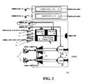
- FIG 3 illustrates one preferred embodiment of a device 100 which is powered by a power supply voltage VBAT (between 2.3V and 4.8V in accordance with the status of the battery (not shown).
- device 100 is assumed to include two conventional SMPS circuits 41 and 42, which are associated with appropriate external components, ie coil and capacitor, for the purpose of generating a fixed output voltage, e.g. 1.8 Volts or 1.2. Volts according to the case.
- SMPS circuits 41 and 42 may be embodied by means of any known SMPS circuit well known to a skilled man and such circuit will not be further elaborated on.
- SMPS circuits 41 and 42 resp. SMPS VI/O_1V8 and SMPS VI/O_1.2V
- SMPS VI/O_1.2V two specific SMPS circuits 41 and 42, resp. SMPS VI/O_1V8 and SMPS VI/O_1.2V), which are assumed to provide two respective voltages (1.8V; 1.2V) used for powering some dedicated Input/output interfaces.
- Device 100 is arranged to offer specific audio capabilities and connections to two loudspeakers or to a headset 15.
- device 100 comprises specific audio circuits, e.g. a AB class audio amplifier embodied by internal block 44 (AS_INT) and external blocks 45-46 (AB_EXT), the audio amplifier being arranged to drive first and second loudspeakers 15, or a headset in accordance with analog signals generated by DAC circuits 14, for instance resulting from a digital audio file stored within the memory (not represented in the figure).
- AS_INT internal block 44
- AB_EXT external blocks 45-46
- the embodiment includes, in addition to the pre-existing SMPS, a dual voltage charge pump 43 which is powered by SMPS VI/O_1V8 circuit 41 and by counterpart SMPSVI/O1V2 circuit 42.
- the dual output CHARGE_PUMP provides both modulated supply (POSITIVE and NEGATIVE) on the range ⁇ 1.7V; ⁇ 1.1V, ⁇ 0.7V and ⁇ 0.5V which are used for supplying voltage to the audio amplifier, taking into account the voltage losses existing in the MOS switches.
- a charge pump is conventionally based on one capacitor - known as a " fly or flying capacitor” - which serves for the transfer of charge to one or more " tank “ or " reservoir “ capacitor.
- dual voltage charge pump 43 is associated to four external capacitors, respectively a first and second flying or fly capacitors 32 and 33 and first and second reservoir or tank capacitors 31 and 34.
- the charge pump In order to maximize the amplitude of the audio signal the charge pump provides a set of two high output voltage ( ⁇ 1.7V; ⁇ 1.1V) on the audio amplifier with the structure below. However, in order to minimize power consumption for small audio signals, a second set of two low output voltages ( ⁇ 0.7V and ⁇ 0.5V) is generated by dual charge pump 12 which will now be more precisely described in reference with figure 4 .
- charge pump 43 includes a first PMOS transistor 102 having source and drain terminals, and a gate terminal which receives a control signal NPH1L.
- the source of PMOS transistor 102 is connected to the first source of voltage Vdd1 generated by the first SMPS circuit (and assumed to receiver the supply voltage having the higher value) while its drain is connected to a first end (CCP2) of the first fly capacitor 32 (represented in figure 4 with its internal resistor designated by the generic name ESR) and also to the drain of a first NMOS transistor 122 which source is connected to ground.
- Transistor 122 has a gate terminal which receives a control signal NPH2L.
- Fly capacitor 32 has a second end (CCN2) which is connected to the train terminal of a second NMOS transistor 123 having its source terminal connected to the ground a gate terminal for receiving a control signal NPH1H.
- Charge pump 43 comprises a third NMOS transistor 126 having source and drain terminals, and a gate receiving a control voltage NPH2H.
- the source of transistor 126 is connected to the second end (CCN2) of the first fly capacitor 32, while the drain of transistor 126 is connected to the first end of tank capacitor 31 (which losses are illustrated by means of a resistor in figure 4 ), having its other end connected to ground, and which is coupled in parallel to a negative load 150.
- Charge pump 43 further includes a second PMOS transistor 112 having source and drain terminals, and a gate terminal which receives a control signal NPH2L.
- the source of PMOS transistor 112 is connected to the second voltage source Vdd2 generated by the second SMPS circuit (and providing the supply voltage with the lower level) while its drain is connected to first end (CCP2) of first fly capacitor 32 as well as to the drain of first NMOS transistor 122.
- Charge pump 43 further includes a third PMOS transistor 101 having source and drain terminals as well as a gate terminal for receiving a control signal PPH1L.
- the source of PMOS transistor 101 is connected to Vdd1 (generated by SMPS VI/O_1V8 producing 1.8Volt) while its drain is connected to a first end of a second tank capacitor 34.
- Tank capacitor 34 (which losses are represented by a ESR resistor connected in series) has a second end which is connected to the ground.
- a load 151 is connected in parallel to the tank capacitor 34 which represents the current load of the audio driver.
- Charge pump 43 further includes a fourth PMOS transistor 111 having source and drain terminals as well as a gate terminal for receiving a control signal PPH2L.
- the source of PMOS transistor 111 is connected to second voltage Vdd2 (assumed to receive the supply voltage having the lower value) generated by the second fixed SMPS (SMPS VI/O_1V2 producing 1.2Volt) while its drain is connected to the first end of tank capacitor 34.
- Charge pump 43 further comprises a fourth NMOS transistor 124 which has source and drain terminals, and a gate terminal for receiving a control signal PPS2L.
- the source terminal of NMOS transistor 124 is connected to the second end (CCN2) of first fly capacitor 32 while the drain terminal of NMOS transistor 124 is connected to a first end of second fly capacitor 33 (which losses are illustrated by a resistor in figure 4 ), which second end is connected to ground.
- charge pump 43 further comprises a fifth PMOS transistor 125 which has source and drain terminals, and a gate terminal for receiving a control signal PPH3L.
- the source terminal of PMOS transistor 125 is connected to the first end (CCP1) of second fly capacitor 33, while the drain of the same transistor is connected to the first end of tank capacitor 34.
- the circuit is capable of generating various positive Vpos and negative Vneg may be used for driving a AB class amplifier, or even a H class amplifier thanks to the possibility of generating, as will become apparent hereinafter with the subsequent drawings of figures 5 and 6 , four distinctive positive and four distinctive negative voltages.
- Charge pump 43 is arranged to provide, from the fixed positive voltage Vdd1 (assumed to have the higher voltage) generated by first SMPS (VDD_1.V8), the set of voltages ⁇ 1.7V.
- the dual charge pump operates as follows:
- the tank capacitor may be charged with a voltage of about 1.7 Volts.
- Charge pump 43 is arranged to provide, from the fixed positive voltage Vdd2 (assumed to have the lower voltage level) generated by the second SMPS (VDD_1.V2), the second higher voltage ⁇ 1.1V.
- the dual charge pump operates as follows:
- the tank capacitor may be charged with a voltage of about 1.1 Volts.
- Vdd2 1.2V
- the process is controlled by means of the application of appropriate control signals to the gate of transistors 101-102-111-125 and 122-123-126 and the generation of such control signals is well known to a skilled man and will not be further elaborated on.
- Charge pump 43 is arranged to provide, from the fixed positive voltage Vdd1 generated by first SMPS (VDD_1.V8), the third voltage ⁇ 0.7V
- the dual charge pump operates as follows as illustrated in figure 6 :
- transistors 102 and 124 are switched ON while all other transistors are switched OFF, so as to establish a connection in series of the two fly capacitors 32 and 33 between Vdd1 and the ground.
- all transistors 101-102-111-125 and 122-123-126 receive the application of adequate control signals so as to achieve the sequence of phases described above.
- Charge pump 43 is arranged to provide, from the fixed positive voltage Vdd2 generated by the second SMPS (VDD_1.V8), the lowest voltage (in absolute value) ⁇ 0.5V. This is achieved as follows:
- the dual charge pump operates as follows as illustrated in figure 6 :
- transistor 112 and 124 are switched ON while all other transistors are switched OFF, so as to establish a connection in series of the two fly capacitors 32 and 33 between Vdd2 and the ground.
- the tank capacitors can be charged so as to produce a low voltage of about ⁇ 0.55V .
- all transistors 101-102-111-125 and 122-123-126 receive the application of adequate control signals so as to achieve the sequence of phases described above.
- the generation of the different control signals applied to the gates of the transistors can be performed so as to control the generation of the low or high voltage in accordance with the actual level of an analog signal, thus achieving the voltage supply of a H class audio amplifier.
- the playing of the audio file is slightly delayed so as to permit adequate signal processing and achieve the appropriate control of the set of switches 101-102-111-125 and 122-123-126 as the audio file is being played by the user.
- a processing of the delayed audio file by a processor for the purpose of entering into an analysis of the volume of the analog signal so as to generate the appropriate control signals for the gates of all transistors, ensuring adequate powering of the AB class audio amplifier.
- the inventors have discovered that, thanks to such mechanism, it was possible to save about 3.5 mW on a typical audio file which would have normally require about 10-12 mW.
- FIG 7 there is now illustrated one particular embodiment of a multi level charge pump circuit which can be used for generating negative voltage only.
- Such embodiment is based on the particular components illustrated in figure 4 which are involved for the generation of the negative voltage only. Therefore, for the sake of clarity, the components which are common to those of figure 4 bear the same reference number.
- the negative multilevel charge pump comprises one single fly capacitor 32 and one single tank capacitor 31, having one end connected to the ground.
- the circuit comprises:
- Such arrangement achieves the generation of different negative voltage levels by successive charge transfer from either the first power supply (Vdd1) or the second power supply (Vdd2) into fly capacitor 32, then followed by a corresponding transfer of charge into the tank capacitor 31.
Landscapes
- Engineering & Computer Science (AREA)
- Physics & Mathematics (AREA)
- Theoretical Computer Science (AREA)
- General Physics & Mathematics (AREA)
- Power Engineering (AREA)
- General Engineering & Computer Science (AREA)
- Human Computer Interaction (AREA)
- General Health & Medical Sciences (AREA)
- Audiology, Speech & Language Pathology (AREA)
- Health & Medical Sciences (AREA)
- Multimedia (AREA)
- Electromagnetism (AREA)
- Radar, Positioning & Navigation (AREA)
- Automation & Control Theory (AREA)
- Dc-Dc Converters (AREA)
- Amplifiers (AREA)
Priority Applications (2)
| Application Number | Priority Date | Filing Date | Title |
|---|---|---|---|
| EP13368024.9A EP2840694A1 (de) | 2013-08-20 | 2013-08-20 | Mehrstufige Ladungspumpe zur Erzeugung von vier Spannungen mit vier unterschiedlichen Stufen sowie Verfahren dafür |
| US14/461,780 US9225238B2 (en) | 2013-08-20 | 2014-08-18 | Multiple level charge pump generating voltages with distinct levels and associated methods |
Applications Claiming Priority (1)
| Application Number | Priority Date | Filing Date | Title |
|---|---|---|---|
| EP13368024.9A EP2840694A1 (de) | 2013-08-20 | 2013-08-20 | Mehrstufige Ladungspumpe zur Erzeugung von vier Spannungen mit vier unterschiedlichen Stufen sowie Verfahren dafür |
Publications (1)
| Publication Number | Publication Date |
|---|---|
| EP2840694A1 true EP2840694A1 (de) | 2015-02-25 |
Family
ID=49231407
Family Applications (1)
| Application Number | Title | Priority Date | Filing Date |
|---|---|---|---|
| EP13368024.9A Withdrawn EP2840694A1 (de) | 2013-08-20 | 2013-08-20 | Mehrstufige Ladungspumpe zur Erzeugung von vier Spannungen mit vier unterschiedlichen Stufen sowie Verfahren dafür |
Country Status (2)
| Country | Link |
|---|---|
| US (1) | US9225238B2 (de) |
| EP (1) | EP2840694A1 (de) |
Cited By (1)
| Publication number | Priority date | Publication date | Assignee | Title |
|---|---|---|---|---|
| CN109565261A (zh) * | 2016-11-22 | 2019-04-02 | 华为技术有限公司 | 一种供电电路及音频播放设备 |
Families Citing this family (2)
| Publication number | Priority date | Publication date | Assignee | Title |
|---|---|---|---|---|
| EP2587648A1 (de) | 2011-10-28 | 2013-05-01 | ST-Ericsson SA | Ladungspumpenschaltkreis |
| KR102547951B1 (ko) | 2016-09-20 | 2023-06-26 | 삼성전자주식회사 | 재구성 가능한 양극성 출력 차지 펌프 회로 및 이를 포함하는 집적 회로 |
Citations (3)
| Publication number | Priority date | Publication date | Assignee | Title |
|---|---|---|---|---|
| US20100321099A1 (en) * | 2009-06-22 | 2010-12-23 | Richtek Technology Corp. | Efficiency and thermal improvement of a charge pump by mixing different input voltages |
| WO2012025232A2 (en) * | 2010-08-26 | 2012-03-01 | St-Ericsson Sa | Dual output charge pump generating two voltage values with two distinctive levels, and method for the same |
| EP2469694A1 (de) * | 2010-12-23 | 2012-06-27 | Wolfson Microelectronics plc | Ladepumpenschaltung |
Family Cites Families (4)
| Publication number | Priority date | Publication date | Assignee | Title |
|---|---|---|---|---|
| US7884665B2 (en) * | 2005-12-08 | 2011-02-08 | Rohm Co., Ltd. | Charge pump circuit, LCD driver IC, and electronic appliance |
| US7427889B2 (en) * | 2006-04-28 | 2008-09-23 | Ememory Technology Inc. | Voltage regulator outputting positive and negative voltages with the same offsets |
| US7382195B2 (en) * | 2006-08-11 | 2008-06-03 | Anpec Electronics Corporation | Power supply device for driving an amplifier |
| US8311243B2 (en) * | 2006-08-21 | 2012-11-13 | Cirrus Logic, Inc. | Energy-efficient consumer device audio power output stage |
-
2013
- 2013-08-20 EP EP13368024.9A patent/EP2840694A1/de not_active Withdrawn
-
2014
- 2014-08-18 US US14/461,780 patent/US9225238B2/en active Active
Patent Citations (3)
| Publication number | Priority date | Publication date | Assignee | Title |
|---|---|---|---|---|
| US20100321099A1 (en) * | 2009-06-22 | 2010-12-23 | Richtek Technology Corp. | Efficiency and thermal improvement of a charge pump by mixing different input voltages |
| WO2012025232A2 (en) * | 2010-08-26 | 2012-03-01 | St-Ericsson Sa | Dual output charge pump generating two voltage values with two distinctive levels, and method for the same |
| EP2469694A1 (de) * | 2010-12-23 | 2012-06-27 | Wolfson Microelectronics plc | Ladepumpenschaltung |
Non-Patent Citations (1)
| Title |
|---|
| KEI EGUCHI: "Design of a Hybrid Input Charge-Pump Utilizing Waste Heat and Its Thermal Analysis Method", INTELLIGENT NETWORKS AND INTELLIGENT SYSTEMS (ICINIS), 2011 4TH INTERNATIONAL CONFERENCE ON, IEEE, 1 November 2011 (2011-11-01), pages 137 - 140, XP032075132, ISBN: 978-1-4577-1626-3, DOI: 10.1109/ICINIS.2011.17 * |
Cited By (2)
| Publication number | Priority date | Publication date | Assignee | Title |
|---|---|---|---|---|
| CN109565261A (zh) * | 2016-11-22 | 2019-04-02 | 华为技术有限公司 | 一种供电电路及音频播放设备 |
| US10998858B2 (en) | 2016-11-22 | 2021-05-04 | Huawei Technologies Co., Ltd. | Power supply circuit and audio play device |
Also Published As
| Publication number | Publication date |
|---|---|
| US20150055805A1 (en) | 2015-02-26 |
| US9225238B2 (en) | 2015-12-29 |
Similar Documents
| Publication | Publication Date | Title |
|---|---|---|
| JP5934759B2 (ja) | チャージポンプ回路およびその動作方法 | |
| US8363856B2 (en) | Audio amplifier circuit and electronic apparatus including the same | |
| CN106549564B (zh) | 具有供给调制的功率放大设备和方法 | |
| US10848061B2 (en) | Switching power converter | |
| US20120049936A1 (en) | Charge Pump Circuits and Methods | |
| US8804386B2 (en) | Charge pump circuit with pulse-width modulation | |
| CN102104365A (zh) | 功率放大电路、dc-dc转换器、峰值保持电路和输出电压控制电路 | |
| CN106487343B (zh) | 用于d类放大器的功率级的驱动器电路 | |
| CN106549471B (zh) | 功率管理电路 | |
| US10910947B2 (en) | Single inductor multiple output regulator with hybrid negative and positive rail generation | |
| US11606642B2 (en) | Driver circuits | |
| US20070063762A1 (en) | Semiconductor device with charge pump booster circuit | |
| US20230030111A1 (en) | Driver circuitry | |
| EP2840694A1 (de) | Mehrstufige Ladungspumpe zur Erzeugung von vier Spannungen mit vier unterschiedlichen Stufen sowie Verfahren dafür | |
| US8698550B2 (en) | Dual output charge pump generating two voltage values with two distinctive levels, and method for the same | |
| JP2014039109A (ja) | 電力増幅器および送信器 | |
| US11381239B1 (en) | Driver circuitry | |
| CN210629440U (zh) | 功率管栅极驱动电路及集成电路 | |
| CN102761243B (zh) | 自适应电荷泵 | |
| GB2561923B (en) | Power converter predriver system with multiple power modes | |
| GB2475633A (en) | An audio amplifier supplied by a reconfigurable charge pump and operable to drive either headphones or a line output |
Legal Events
| Date | Code | Title | Description |
|---|---|---|---|
| PUAI | Public reference made under article 153(3) epc to a published international application that has entered the european phase |
Free format text: ORIGINAL CODE: 0009012 |
|
| 17P | Request for examination filed |
Effective date: 20130820 |
|
| AK | Designated contracting states |
Kind code of ref document: A1 Designated state(s): AL AT BE BG CH CY CZ DE DK EE ES FI FR GB GR HR HU IE IS IT LI LT LU LV MC MK MT NL NO PL PT RO RS SE SI SK SM TR |
|
| AX | Request for extension of the european patent |
Extension state: BA ME |
|
| STAA | Information on the status of an ep patent application or granted ep patent |
Free format text: STATUS: THE APPLICATION IS DEEMED TO BE WITHDRAWN |
|
| 18D | Application deemed to be withdrawn |
Effective date: 20150826 |