EP2840605A2 - A semiconductor component having a lateral semiconductor device and a vertical semiconductor device - Google Patents
A semiconductor component having a lateral semiconductor device and a vertical semiconductor device Download PDFInfo
- Publication number
- EP2840605A2 EP2840605A2 EP13183554.8A EP13183554A EP2840605A2 EP 2840605 A2 EP2840605 A2 EP 2840605A2 EP 13183554 A EP13183554 A EP 13183554A EP 2840605 A2 EP2840605 A2 EP 2840605A2
- Authority
- EP
- European Patent Office
- Prior art keywords
- semiconductor device
- electrode
- lateral
- vertical
- component according
- Prior art date
- Legal status (The legal status is an assumption and is not a legal conclusion. Google has not performed a legal analysis and makes no representation as to the accuracy of the status listed.)
- Granted
Links
Images



Classifications
-
- H—ELECTRICITY
- H10—SEMICONDUCTOR DEVICES; ELECTRIC SOLID-STATE DEVICES NOT OTHERWISE PROVIDED FOR
- H10W—GENERIC PACKAGES, INTERCONNECTIONS, CONNECTORS OR OTHER CONSTRUCTIONAL DETAILS OF DEVICES COVERED BY CLASS H10
- H10W70/00—Package substrates; Interposers; Redistribution layers [RDL]
- H10W70/40—Leadframes
-
- H—ELECTRICITY
- H10—SEMICONDUCTOR DEVICES; ELECTRIC SOLID-STATE DEVICES NOT OTHERWISE PROVIDED FOR
- H10W—GENERIC PACKAGES, INTERCONNECTIONS, CONNECTORS OR OTHER CONSTRUCTIONAL DETAILS OF DEVICES COVERED BY CLASS H10
- H10W70/00—Package substrates; Interposers; Redistribution layers [RDL]
- H10W70/40—Leadframes
- H10W70/464—Additional interconnections in combination with leadframes
- H10W70/466—Tape carriers or flat leads
-
- H—ELECTRICITY
- H10—SEMICONDUCTOR DEVICES; ELECTRIC SOLID-STATE DEVICES NOT OTHERWISE PROVIDED FOR
- H10W—GENERIC PACKAGES, INTERCONNECTIONS, CONNECTORS OR OTHER CONSTRUCTIONAL DETAILS OF DEVICES COVERED BY CLASS H10
- H10W70/00—Package substrates; Interposers; Redistribution layers [RDL]
- H10W70/40—Leadframes
- H10W70/481—Leadframes for devices being provided for in groups H10D8/00 - H10D48/00
-
- H—ELECTRICITY
- H10—SEMICONDUCTOR DEVICES; ELECTRIC SOLID-STATE DEVICES NOT OTHERWISE PROVIDED FOR
- H10W—GENERIC PACKAGES, INTERCONNECTIONS, CONNECTORS OR OTHER CONSTRUCTIONAL DETAILS OF DEVICES COVERED BY CLASS H10
- H10W72/00—Interconnections or connectors in packages
- H10W72/60—Strap connectors, e.g. thick copper clips for grounding of power devices
-
- H—ELECTRICITY
- H10—SEMICONDUCTOR DEVICES; ELECTRIC SOLID-STATE DEVICES NOT OTHERWISE PROVIDED FOR
- H10W—GENERIC PACKAGES, INTERCONNECTIONS, CONNECTORS OR OTHER CONSTRUCTIONAL DETAILS OF DEVICES COVERED BY CLASS H10
- H10W90/00—Package configurations
-
- H—ELECTRICITY
- H10—SEMICONDUCTOR DEVICES; ELECTRIC SOLID-STATE DEVICES NOT OTHERWISE PROVIDED FOR
- H10W—GENERIC PACKAGES, INTERCONNECTIONS, CONNECTORS OR OTHER CONSTRUCTIONAL DETAILS OF DEVICES COVERED BY CLASS H10
- H10W90/00—Package configurations
- H10W90/811—Multiple chips on leadframes
-
- H—ELECTRICITY
- H10—SEMICONDUCTOR DEVICES; ELECTRIC SOLID-STATE DEVICES NOT OTHERWISE PROVIDED FOR
- H10W—GENERIC PACKAGES, INTERCONNECTIONS, CONNECTORS OR OTHER CONSTRUCTIONAL DETAILS OF DEVICES COVERED BY CLASS H10
- H10W20/00—Interconnections in chips, wafers or substrates
- H10W20/40—Interconnections external to wafers or substrates, e.g. back-end-of-line [BEOL] metallisations or vias connecting to gate electrodes
- H10W20/41—Interconnections external to wafers or substrates, e.g. back-end-of-line [BEOL] metallisations or vias connecting to gate electrodes characterised by their conductive parts
- H10W20/43—Layouts of interconnections
- H10W20/432—Layouts of interconnections comprising crossing interconnections
-
- H—ELECTRICITY
- H10—SEMICONDUCTOR DEVICES; ELECTRIC SOLID-STATE DEVICES NOT OTHERWISE PROVIDED FOR
- H10W—GENERIC PACKAGES, INTERCONNECTIONS, CONNECTORS OR OTHER CONSTRUCTIONAL DETAILS OF DEVICES COVERED BY CLASS H10
- H10W70/00—Package substrates; Interposers; Redistribution layers [RDL]
- H10W70/40—Leadframes
- H10W70/464—Additional interconnections in combination with leadframes
- H10W70/465—Bumps or wires
-
- H—ELECTRICITY
- H10—SEMICONDUCTOR DEVICES; ELECTRIC SOLID-STATE DEVICES NOT OTHERWISE PROVIDED FOR
- H10W—GENERIC PACKAGES, INTERCONNECTIONS, CONNECTORS OR OTHER CONSTRUCTIONAL DETAILS OF DEVICES COVERED BY CLASS H10
- H10W70/00—Package substrates; Interposers; Redistribution layers [RDL]
- H10W70/40—Leadframes
- H10W70/464—Additional interconnections in combination with leadframes
- H10W70/467—Multilayered additional interconnections
-
- H—ELECTRICITY
- H10—SEMICONDUCTOR DEVICES; ELECTRIC SOLID-STATE DEVICES NOT OTHERWISE PROVIDED FOR
- H10W—GENERIC PACKAGES, INTERCONNECTIONS, CONNECTORS OR OTHER CONSTRUCTIONAL DETAILS OF DEVICES COVERED BY CLASS H10
- H10W70/00—Package substrates; Interposers; Redistribution layers [RDL]
- H10W70/40—Leadframes
- H10W70/464—Additional interconnections in combination with leadframes
- H10W70/468—Circuit boards
-
- H—ELECTRICITY
- H10—SEMICONDUCTOR DEVICES; ELECTRIC SOLID-STATE DEVICES NOT OTHERWISE PROVIDED FOR
- H10W—GENERIC PACKAGES, INTERCONNECTIONS, CONNECTORS OR OTHER CONSTRUCTIONAL DETAILS OF DEVICES COVERED BY CLASS H10
- H10W72/00—Interconnections or connectors in packages
- H10W72/071—Connecting or disconnecting
- H10W72/076—Connecting or disconnecting of strap connectors
- H10W72/07651—Connecting or disconnecting of strap connectors characterised by changes in properties of the strap connectors during connecting
- H10W72/07653—Connecting or disconnecting of strap connectors characterised by changes in properties of the strap connectors during connecting changes in shapes
-
- H—ELECTRICITY
- H10—SEMICONDUCTOR DEVICES; ELECTRIC SOLID-STATE DEVICES NOT OTHERWISE PROVIDED FOR
- H10W—GENERIC PACKAGES, INTERCONNECTIONS, CONNECTORS OR OTHER CONSTRUCTIONAL DETAILS OF DEVICES COVERED BY CLASS H10
- H10W72/00—Interconnections or connectors in packages
- H10W72/60—Strap connectors, e.g. thick copper clips for grounding of power devices
- H10W72/651—Materials of strap connectors
- H10W72/652—Materials of strap connectors comprising metals or metalloids, e.g. silver
-
- H—ELECTRICITY
- H10—SEMICONDUCTOR DEVICES; ELECTRIC SOLID-STATE DEVICES NOT OTHERWISE PROVIDED FOR
- H10W—GENERIC PACKAGES, INTERCONNECTIONS, CONNECTORS OR OTHER CONSTRUCTIONAL DETAILS OF DEVICES COVERED BY CLASS H10
- H10W72/00—Interconnections or connectors in packages
- H10W72/851—Dispositions of multiple connectors or interconnections
- H10W72/853—On the same surface
- H10W72/871—Bond wires and strap connectors
-
- H—ELECTRICITY
- H10—SEMICONDUCTOR DEVICES; ELECTRIC SOLID-STATE DEVICES NOT OTHERWISE PROVIDED FOR
- H10W—GENERIC PACKAGES, INTERCONNECTIONS, CONNECTORS OR OTHER CONSTRUCTIONAL DETAILS OF DEVICES COVERED BY CLASS H10
- H10W72/00—Interconnections or connectors in packages
- H10W72/851—Dispositions of multiple connectors or interconnections
- H10W72/874—On different surfaces
- H10W72/881—Bump connectors and strap connectors
-
- H—ELECTRICITY
- H10—SEMICONDUCTOR DEVICES; ELECTRIC SOLID-STATE DEVICES NOT OTHERWISE PROVIDED FOR
- H10W—GENERIC PACKAGES, INTERCONNECTIONS, CONNECTORS OR OTHER CONSTRUCTIONAL DETAILS OF DEVICES COVERED BY CLASS H10
- H10W72/00—Interconnections or connectors in packages
- H10W72/90—Bond pads, in general
- H10W72/921—Structures or relative sizes of bond pads
- H10W72/926—Multiple bond pads having different sizes
-
- H—ELECTRICITY
- H10—SEMICONDUCTOR DEVICES; ELECTRIC SOLID-STATE DEVICES NOT OTHERWISE PROVIDED FOR
- H10W—GENERIC PACKAGES, INTERCONNECTIONS, CONNECTORS OR OTHER CONSTRUCTIONAL DETAILS OF DEVICES COVERED BY CLASS H10
- H10W72/00—Interconnections or connectors in packages
- H10W72/90—Bond pads, in general
- H10W72/941—Dispositions of bond pads
- H10W72/944—Dispositions of multiple bond pads
-
- H—ELECTRICITY
- H10—SEMICONDUCTOR DEVICES; ELECTRIC SOLID-STATE DEVICES NOT OTHERWISE PROVIDED FOR
- H10W—GENERIC PACKAGES, INTERCONNECTIONS, CONNECTORS OR OTHER CONSTRUCTIONAL DETAILS OF DEVICES COVERED BY CLASS H10
- H10W74/00—Encapsulations, e.g. protective coatings
- H10W74/10—Encapsulations, e.g. protective coatings characterised by their shape or disposition
- H10W74/111—Encapsulations, e.g. protective coatings characterised by their shape or disposition the semiconductor body being completely enclosed
-
- H—ELECTRICITY
- H10—SEMICONDUCTOR DEVICES; ELECTRIC SOLID-STATE DEVICES NOT OTHERWISE PROVIDED FOR
- H10W—GENERIC PACKAGES, INTERCONNECTIONS, CONNECTORS OR OTHER CONSTRUCTIONAL DETAILS OF DEVICES COVERED BY CLASS H10
- H10W74/00—Encapsulations, e.g. protective coatings
- H10W74/10—Encapsulations, e.g. protective coatings characterised by their shape or disposition
- H10W74/131—Encapsulations, e.g. protective coatings characterised by their shape or disposition the semiconductor body being only partially enclosed
- H10W74/137—Encapsulations, e.g. protective coatings characterised by their shape or disposition the semiconductor body being only partially enclosed the encapsulations being directly on the semiconductor body
-
- H—ELECTRICITY
- H10—SEMICONDUCTOR DEVICES; ELECTRIC SOLID-STATE DEVICES NOT OTHERWISE PROVIDED FOR
- H10W—GENERIC PACKAGES, INTERCONNECTIONS, CONNECTORS OR OTHER CONSTRUCTIONAL DETAILS OF DEVICES COVERED BY CLASS H10
- H10W90/00—Package configurations
- H10W90/701—Package configurations characterised by the relative positions of pads or connectors relative to package parts
- H10W90/721—Package configurations characterised by the relative positions of pads or connectors relative to package parts of bump connectors
- H10W90/726—Package configurations characterised by the relative positions of pads or connectors relative to package parts of bump connectors between a chip and a stacked lead frame, conducting package substrate or heat sink
-
- H—ELECTRICITY
- H10—SEMICONDUCTOR DEVICES; ELECTRIC SOLID-STATE DEVICES NOT OTHERWISE PROVIDED FOR
- H10W—GENERIC PACKAGES, INTERCONNECTIONS, CONNECTORS OR OTHER CONSTRUCTIONAL DETAILS OF DEVICES COVERED BY CLASS H10
- H10W90/00—Package configurations
- H10W90/701—Package configurations characterised by the relative positions of pads or connectors relative to package parts
- H10W90/731—Package configurations characterised by the relative positions of pads or connectors relative to package parts of die-attach connectors
- H10W90/732—Package configurations characterised by the relative positions of pads or connectors relative to package parts of die-attach connectors between stacked chips
-
- H—ELECTRICITY
- H10—SEMICONDUCTOR DEVICES; ELECTRIC SOLID-STATE DEVICES NOT OTHERWISE PROVIDED FOR
- H10W—GENERIC PACKAGES, INTERCONNECTIONS, CONNECTORS OR OTHER CONSTRUCTIONAL DETAILS OF DEVICES COVERED BY CLASS H10
- H10W90/00—Package configurations
- H10W90/701—Package configurations characterised by the relative positions of pads or connectors relative to package parts
- H10W90/731—Package configurations characterised by the relative positions of pads or connectors relative to package parts of die-attach connectors
- H10W90/736—Package configurations characterised by the relative positions of pads or connectors relative to package parts of die-attach connectors between a chip and a stacked lead frame, conducting package substrate or heat sink
-
- H—ELECTRICITY
- H10—SEMICONDUCTOR DEVICES; ELECTRIC SOLID-STATE DEVICES NOT OTHERWISE PROVIDED FOR
- H10W—GENERIC PACKAGES, INTERCONNECTIONS, CONNECTORS OR OTHER CONSTRUCTIONAL DETAILS OF DEVICES COVERED BY CLASS H10
- H10W90/00—Package configurations
- H10W90/701—Package configurations characterised by the relative positions of pads or connectors relative to package parts
- H10W90/751—Package configurations characterised by the relative positions of pads or connectors relative to package parts of bond wires
- H10W90/756—Package configurations characterised by the relative positions of pads or connectors relative to package parts of bond wires between a chip and a stacked lead frame, conducting package substrate or heat sink
-
- H—ELECTRICITY
- H10—SEMICONDUCTOR DEVICES; ELECTRIC SOLID-STATE DEVICES NOT OTHERWISE PROVIDED FOR
- H10W—GENERIC PACKAGES, INTERCONNECTIONS, CONNECTORS OR OTHER CONSTRUCTIONAL DETAILS OF DEVICES COVERED BY CLASS H10
- H10W90/00—Package configurations
- H10W90/701—Package configurations characterised by the relative positions of pads or connectors relative to package parts
- H10W90/761—Package configurations characterised by the relative positions of pads or connectors relative to package parts of strap connectors
- H10W90/766—Package configurations characterised by the relative positions of pads or connectors relative to package parts of strap connectors between a chip and a stacked lead frame, conducting package substrate or heat sink
Definitions
- the present disclosure relates to a semiconductor component, and more particularly, to a semiconductor component in which a stack has both lateral and vertical semiconductor devices.
- III-V compound semiconductors such as Gallium Arsenide (GaAs), Gallium Nitride (GaN) are increasingly being provided, in that the devices made therefrom like high electron mobility transistors (HEMTs) are known possessing special characteristics e.g., in high-power performance, different from conventional silicon-based semiconductors.
- GaAs Gallium Arsenide
- GaN Gallium Nitride
- HEMTs high electron mobility transistors
- the formation of the conductive channel of a III-V compound semiconductor device applies the difference between the band gaps of the respective layers in the devices. Due to the band gaps vary among the layers, a two-dimensional electron gas (2DEG) is formed at the interface of these layers.
- the 2DEG serves as a conductive channel, as that disclosed in the US Patent Nos. 5,192,987 and 6,849,882 .
- a lateral semiconductor device which the source, drain, and gate electrodes therein are positioned on the same side of the semiconductor device, is now the only form provided in such III-V compound-based semiconductor devices.
- a semiconductor component in which two or more semiconductor devices are stacked and packaged, has become increasingly popular so as to improve the performance and packaging area thereof. Therefore, it is desirable to provide a semiconductor component which accommodates both lateral semiconductor device and vertical semiconductor device in the stacked semiconductor devices.
- the present disclosure provides a semiconductor component comprising a lateral semiconductor device, a vertical semiconductor device, and a leadframe.
- the lateral semiconductor device has a first side, a second side.
- the lateral semiconductor device has an active region, positioned on the first side, comprising a first electrode, a second electrode, and a control electrode.
- the vertical semiconductor device has a first side and a second side, a first electrode positioned on the first side , a second electrode and a control electrode positioned on the second side.
- the leadframe electrically and respectively connected to each of the first electrode of the lateral semiconductor device, the second electrode of the lateral semiconductor device, the second electrode of the vertical semiconductor device, and the control electrodes, wherein the first side of the vertical semiconductor device is mounted on the second side of the lateral semiconductor device, and wherein the first electrode of the lateral semiconductor device is also electrically connected to the first electrode of the vertical semiconductor device
- the first side of the lateral semiconductor device faces to the leadframe. ( fig.1 , 2 , 3 , 4 , 5 , 6 )
- control electrode of the lateral semiconductor device is electrically connected to the second electrode of the vertical semiconductor device.
- a passivation layer positioned on the first side of the lateral semiconductor device.
- the leadframe comprises a plurality of portions.
- At least two of the plurality of portions are substantially coplanar.
- At least two of the plurality of portions are substantially non-coplanar.
- a first connector electrically connecting the first electrode of the lateral semiconductor device and the first electrode of the vertical semiconductor device.
- the present disclosure further comprising a conductive layer on the second side of the lateral semiconductor device, wherein the first electrode of the vertical semiconductor device contacts the conductive layer, and the first connector electrically connects the first electrode of the lateral semiconductor device and the conductive layer.
- the first connector comprises a clip, ribbon, or bonding-wire.
- a second connector contacts both the second electrode of the vertical semiconductor and the leadframe.
- the second connector comprises a clip, ribbon, or bonding-wire.
- a third connector contacts both the control electrode of the vertical semiconductor device and the leadframe.
- the third connector comprises a clip, ribbon, or bonding-wire.
- the lateral semiconductor device comprises a metal-insulator-semiconductor field-effect transistor (MISFET), a metal semiconductor field effect transistor (MESFET), or a High-electron-mobility transistor (HEMT).
- MISFET metal-insulator-semiconductor field-effect transistor
- MESFT metal semiconductor field effect transistor
- HEMT High-electron-mobility transistor
- the lateral semiconductor device comprises a nitride-based power transistor.
- the first electrode of the lateral semiconductor device is a source electrode
- the second electrode of the lateral semiconductor device is a drain electrode
- the first electrode of the vertical semiconductor device is a drain electrode
- the second electrode of the vertical semiconductor device is a source electrode
- the control electrodes of the lateral and the vertical semiconductor devices are gate electrodes.
- the lateral semiconductor device has a thickness larger than that of the vertical semiconductor device.
- the semiconductor component 100 of the present disclosure comprises a lateral semiconductor device 110, a vertical semiconductor device 120, and a leadframe 130.
- the lateral semiconductor device 110 has a first side 111 and a second side 112. As illustrated in Fig.1 , the second side 112 refers to the upper surface of the lateral semiconductor device 110; and the first side 111 refers to the lower surface of the lateral semiconductor device 110.
- the lateral semiconductor device 110 also has an active region, positioned on the first side 111, comprising a first electrode 113, a second electrode 114, and a control electrode 115 positioned on the first side 111 (the lower surface).
- the lateral semiconductor device 110 of the present disclosure can be metal-insulator-semiconductor field-effect transistor (MISFET), a metal semiconductor field effect transistor (MESFET) or a High-electron-mobility transistor (HEMT), which is made of a silicon-based semiconductor or a compound semiconductor and not limited to it.
- the first electrode 113 of the lateral semiconductor device is a source electrode
- the second electrode 114 of the lateral semiconductor device is a drain electrode
- the control electrode 115 of the lateral semiconductor device is a gate electrode.
- the lateral semiconductor device 110 is a HEMT device, which includes several wide bandgap material layers, such as III-V semiconductor layers.
- the lateral semiconductor device comprises a channel layer made of GaN and a barrier layer made of AlGaN. Due to the different band gaps of the two layers, a two-dimensional electron gas (2DEG) is formed at the interface therebetween, the 2DEG serving as a conductive channel.
- 2DEG two-dimensional electron gas
- the mobility of the electrons as well as the 2D-electron charge carrier density is very high in the two-dimensional electron gas, which is provided in an active region between the first electrode 113 of the lateral semiconductor device 110 (the source electrode) and the second electrode 115 of the lateral semiconductor device 110 (the drain electrode).
- the vertical semiconductor device 120 has a first side 121 and a second side 122. As illustrated in Fig.1 , the second side 122 refers to the upper surface of the vertical semiconductor device 120; and the first side 121 refers to the lower surface of the vertical semiconductor device 120.
- the vertical semiconductor device 120 has a second electrode 124 and a control electrode 125 positioned on the second side 122 (the upper surface), and a first electrode 123 positioned on the first side 121 (the lower surface).
- the vertical semiconductor device 120 of the present disclosure can be one of a metal-oxide-semiconductor field-effect transistor (MOSFET), but not limited to it.
- MOSFET metal-oxide-semiconductor field-effect transistor
- the first electrode 123 of the vertical semiconductor device 120 is a drain electrode
- the second electrode 124 of the vertical semiconductor device 120 is a source electrode
- the control electrode 125 of the vertical semiconductor device 120 is a gate electrode.
- the leadframe 130 electrically and respectively connecting to each of the first electrode 113 of the lateral semiconductor device 110, the second electrode 114 of the lateral semiconductor device 110, the second electrode 124 of the vertical semiconductor device 120, the control electrode 115 of the lateral semiconductor device 110, and the control electrode 125 of the vertical semiconductor device 120.
- the leadframe 130 comprises a plurality of portions. As illustrated in Fig. 1 , the plurality of portions includes portions 131, 132, 133, 134 and 135.
- the portion 131 of the leadframe 130 is electrically connected to the first electrode 113 of the lateral semiconductor device 110; the portion 132 of the leadframe 130 is electrically connected to the second electrode 114 of the lateral semiconductor device 110; the portion 133 of the leadframe 130 is electrically connected to the control electrode 115 of the lateral semiconductor device 110; the portion 134 of the leadframe 130 is electrically connected to the second electrode 124 of the vertical semiconductor device 120; and the portion 135 of the leadframe 130 is electrically connected to the control electrode 125 of the vertical semiconductor device 120.
- the first side 121 of the vertical semiconductor device 120 is mounted on the second side 112 of the lateral semiconductor device 110, and the first electrode 113 of the lateral semiconductor device 110 is also electrically connected to the first electrode 123 of the vertical semiconductor device 120.
- the first side 111 of the lateral semiconductor device 110 faces to the leadframe 130.
- the first electrode 113, the second electrode 114, and the control electrode 115 of the lateral semiconductor device 110 are respectively flip-chip bonded to the portion 131 of the leadframe 130, the portion 132 of the leadframe 130, and the portion 133 of the leadframe 130.
- the first electrode 113, the second electrode 114, and the control electrode 115 of the lateral semiconductor device 110 are disposed on their corresponding portions 131, 132, and 133 of the leadframe 130.
- all electrodes (the first electrode 113, the second electrode 114, and the control electrode 115) of the lateral semiconductor device 110 of the present disclosure can be bonded to their corresponding leadframe in a single step, flip-chip bonding, since these electrode are positioned on the same side of the lateral semiconductor device 110.
- the bonding-wires 192 connect the second electrode 124 of the vertical semiconductor device 120 to the portion 134 of the leadframe 130, the control electrode 125 of the vertical semiconductor device 120 to the portion 135 of the leadframe 130, and the first electrode 113 of the lateral semiconductor device 110 to the first electrode 123 of the vertical semiconductor device 120. It should be noticed that one of the bonding-wire 192 is both electrically connected to the first electrode 113 of the lateral semiconductor device 110 and the first electrode 123 of the vertical semiconductor device 120. Therefore, the lateral semiconductor device 110 and the vertical semiconductor device 120 are not only packaged in one stacked structure.
- the bonding-wire 192 comprises one of the gold, gold alloy, aluminum, an aluminum alloy, copper and a copper alloy.
- the first electrode 113 of the lateral semiconductor device 110 is a source electrode
- the second electrode 114 of the lateral semiconductor device 110 is a drain electrode
- the control electrode 125 is a gate electrode of the lateral semiconductor device 110
- the first electrode 123 of the vertical semiconductor device 120 is a drain electrode
- the second electrode 124 of the vertical semiconductor device 120 is a source electrode
- the control electrode 125 is a gate electrode of the vertical semiconductor device 120
- the control electrode 125 of the vertical semiconductor device 120 is a switch to turn on/off the current between the first electrode 123 of the vertical semiconductor device 120 and the second electrode 124 of the vertical semiconductor device 120 by inputting signal to the portion 135 of the leadframe 130; and the control electrode 115 of the lateral semiconductor device 110 is a switch to turn on/off the current between the second electrode 114 of the lateral semiconductor device 110 and the first electrode 113 of the lateral semiconductor device 110 by inputting signal to the portion 133 of the leadframe 130.
- the portion 134 of the leadframe 130 is electrically connected to the portion 133 of the leadframe 130.
- the second electrode 124 of the vertical semiconductor device 120 is electrically connected to the control electrode 115 of the lateral semiconductor device 110.
- the first electrode 113 of the lateral semiconductor device 110 is a drain electrode
- the second electrode 114 of the lateral semiconductor device 110 is a source electrode
- the control electrode 125 is a gate electrode of the lateral semiconductor device 110
- the third electrode 123 is a source electrode
- the second electrode 124 of the vertical semiconductor device 120 is a drain electrode
- the control electrode 125 is a gate electrode of the vertical semiconductor device 120, so as to the current flow within the semiconductor component 100 flows in the portion 134 of the leadframe 130 to the second electrode 124 of the vertical semiconductor device 120, the first electrode 123 of the vertical semiconductor device 120, the portion 131 of the leadframe 130, the first electrode 113 of the lateral semiconductor device 110, the second electrode 114 of the lateral semiconductor device 110, and finally flows out from the portion 132 leadframe 130.
- control electrode 125 of the vertical semiconductor device 120 is a switch to turn on/off the current between the second electrode 124 of the vertical semiconductor device 120 and the first electrode 123 of the vertical semiconductor device 120 by inputting signal to the portion 135 of the leadframe 130; and the control electrode 115 of the lateral semiconductor device 110 is a switch to turn on/off the current between the first electrode 113 of the lateral semiconductor device 110 and the second electrode 114 of the lateral semiconductor device 110 by inputting signal to the portion 133 of the leadframe 130.
- At least two of the plurality of portions are substantially coplanar. As illustrated in Fig.1 , all protions 131, 132, 133,134, and 135 of the leadframe 130are substantially coplanar. Therefore, the signals of input, output, and switch of the semiconductor component 100 can be simply performed by single-side bonding the semiconductor component 100 to. However, in another embodiment of the present disclosure, at least two of the plurality of portions are substantially non-coplanar. The positions of the protions of the leadframe 130 can be altered in different designs, coplanar or non-coplanar, to varieties of needs. As shown in Fig.
- the portion 131 of the leadframe 130, the portion 132 of the leadframe 130, and the portions 133 of the leadframe 130, which are respectively flip-chip bonded to the first electrode 113, the second electrode 114, and the control electrode 115 of the lateral semiconductor device 110, are coplanar (since the first electrode 113, the second electrode 114, and the control electrode 115 are all positioned on the first side 111 of the lateral semiconductor device 110).
- the electrically connections between two elements which are positioned on different height levels are formed by connecting aforementioned elements with bonding-wires 192.
- bonding-wire 192 is not the only option to electrically connect the elements which are positioned on different height levels.
- further comprising a second connector 180 contacts both the second electrode 124 of the vertical semiconductor 120 and the leadframe 130.
- the electrically connection between the portion 131 of the leadframe 130and the first electrode 123 of the vertical semiconductor device 120, and the electrically connection between the portion 134 of the leadframe 130 and the second electrode 124 of the vertical semiconductor device 120 can be formed by applying the first connector 160 and the second connector 180 respectively.
- the first connector 160 comprises a clip, ribbon, or bonding-wire.
- the second connector 180 comprises a clip, ribbon, or bonding-wire.
- the first connector 160 is a metal clip connects both the portion 131 of the leadframe 130 and the first electrode 123 of the vertical semiconductor device 120, such that the first electrode 113 of the lateral semiconductor device 110 is electrically connected to the first electrode 123 of the vertical semiconductor device 120 to form the series connection of the lateral semiconductor device 110 and the vertical semiconductor device 120.
- the second connector 180 is a metal clip connects both the portion 134 of the leadframe 130 and the second electrode 124 of the vertical semiconductor device 120, such that the signal input/output of the semiconductor component 200 can be performed.
- the metal clips has wider cross-section than that of the bonding-wires 192, therefore the capability to carrying current flow of the metal clips is much better than that of the bonding-wires 192.
- the semiconductor component 200 illustrated in Fig. 2 has better capability to be operated in high current flow than that of the semiconductor component 100 illustrated in Fig. 1 .
- the metal clips also have wide surfaces which help diffuse the heat, which is generated in component operation, from the semiconductor component 200 to its surrounding.
- the metal clip may include a material selected from the group of , Ni, Al, Cu, Ag, Au and alloy thereof.
- the control electrode 115 of the lateral semiconductor device 110 is electrically connected to the first electrode 123 of the vertical semiconductor device120.
- the first electrode 113 and the control electrode 115 of the lateral semiconductor device 110 have flip-chip contacts to the common portion 131 of the leadframe 130.
- the control electrode 115 of the lateral semiconductor device 110 does not need to be controlled independently, and its corresponding portion 133 of the leadframe 130, as illustrated in Fig. 1 and Fig. 2 , can be further eliminated.
- the first electrode 113 of the lateral semiconductor device 110 is a source electrode
- the second electrode 114 of the lateral semiconductor device 110 is a drain electrode
- the control electrode 125 is a gate electrode of the lateral semiconductor device 110
- the first electrode 123 of the vertical semiconductor device 120 is a drain electrode
- the second electrode 124 of the vertical semiconductor device 120 is a source electrode
- the control electrode 125 is a gate electrode of the vertical semiconductor device 120
- the control electrode 125 of the vertical semiconductor device 120 is a switch to turn on/off the current between the first electrode 123 and the second electrode 124 of the vertical semiconductor device 120by inputting signal to the portion 135 of the leadframe 130, however, the lateral semiconductor device 110, which is in series connection (also cascode connection) with the vertical semiconductor device 120, does not need to be controlled independently.
- the portion 131 of the leadframe 130 receives the current flow from the second electrode 114 of the lateral semiconductor device 110, the current flow subsequently flows to both the first electrode 113 of the lateral semiconductor device 110 (source electrode) and the control electrode 115 of the lateral semiconductor device 110 (gate electrode) simultaneously.
- the lateral semiconductor device 110 is automatically turning on while vertical semiconductor device 120 is turning on and the current flow flows in its first electrode 113 of the lateral semiconductor device 110 (source electrode) since the current flow also flows in its control electrode 115 of the lateral semiconductor device 110 (gate electrode) in the same time.
- the semiconductor component 300 substantially possesses only one control electrode 125 (gate electrode), positioned on the second side 122 of the vertical semiconductor device 120, to control the series connection (also cascode connection) of the lateral semiconductor device 110 and the vertical semiconductor device 120.
- the selection of the vertical semiconductor device 120 is usually fast switching than that of the lateral semiconductor 110.
- the lateral semiconductor device 110 has a thickness larger than that of the vertical semiconductor device 120.
- the vertical semiconductor device 120 has faster response to driving signals flow in its control electrode 125(gate) than that of the lateral semiconductor device 110. Accordingly, on/off controlling of the semiconductor component 300 is easier and faster since the semiconductor component 300 has a simpler design than that of the semiconductor components 100 and 200.
- the semiconductor 300 further comprises a passivation layer 150 positioned on the first side 111 of the lateral semiconductor device 110.
- the passivation layer 150 is positioned on the first side 111 to cover and protect the active area of the lateral semiconductor device 110.
- the active area includes the current channel between the first electrode 113 and the second electrode 114.
- the passivation layer 150 covers the active area so that the active area is not directly exposed to air or moisture from surrounding, and the lifetime of the lateral semiconductor device 110 is extended.
- the passivation layer 150 may include a material selected from the group of Si x N y , SiO 2 and Al 2 O 3 .
- the passivation layer 150 contacts the portion 131 of the leadframe 130 which have the flip-chip contacts to both the first electrode 113 and the control electrode 115 of the lateral semiconductor device 110.
- the passivation layer 150 receives the heat generated in the active area of the lateral semiconductor device 110 and further diffuses the heat to the portion 131 of the leadframe 130. It reduces the heat accumulation, and increases the reliability of the semiconductor component 300.
- the passivation layer 150 contacts the portion 132 of the leadframe 130which have the flip-chip contact to the second electrode 114 of the lateral semiconductor device 110.
- the passivation layer 150 also receives the heat generated in the active area of the lateral semiconductor device 110 and further diffuses the heat to the portion 132 of the leadframe 130. Similarly, the heat accumulation of the semiconductor module 400 is reduced, and reliability of the semiconductor module 400 is improved.
- the semiconductor component 500 further comprises a conductive layer 170 on the second side of the lateral semiconductor device 110, wherein the first electrode 123 of the vertical semiconductor device 120 contacts the conductive layer 170, and the first connector 160 contacts both the first electrode 113 of the lateral semiconductor device 110 and the conductive layer 170. That is, the first connector 160 does not contact the first electrode 123 of the vertical semiconductor device 120 directly, but contacts the conductive layer 170 which contacts the first electrode 125 of the vertical semiconductor device 120. Therefore, the electrical connection of the first electrode 123 of the vertical semiconductor device 120 and the first electrode 113 of the lateral semiconductor device 110 is also established as the previous embodiments.
- the semiconductor component 600 further comprising a third connector 190 contacts both the control electrode 125 of the vertical semiconductor device 120 and the portion 135 of the leadframe 130, and the electrical connection of the control electrode 125 of the vertical semiconductor device 120 and its corresponding portion 135 of the leadframe 130 is also established as the previous embodiments.
Landscapes
- Junction Field-Effect Transistors (AREA)
- Lead Frames For Integrated Circuits (AREA)
Abstract
Description
- The present disclosure relates to a semiconductor component, and more particularly, to a semiconductor component in which a stack has both lateral and vertical semiconductor devices.
- III-V compound semiconductors such as Gallium Arsenide (GaAs), Gallium Nitride (GaN) are increasingly being provided, in that the devices made therefrom like high electron mobility transistors (HEMTs) are known possessing special characteristics e.g., in high-power performance, different from conventional silicon-based semiconductors.
- Unlike the design rule of silicon-based semiconductor device, the formation of the conductive channel of a III-V compound semiconductor device applies the difference between the band gaps of the respective layers in the devices. Due to the band gaps vary among the layers, a two-dimensional electron gas (2DEG) is formed at the interface of these layers. The 2DEG serves as a conductive channel, as that disclosed in the
US Patent Nos. 5,192,987 and6,849,882 . In this regard, a lateral semiconductor device, which the source, drain, and gate electrodes therein are positioned on the same side of the semiconductor device, is now the only form provided in such III-V compound-based semiconductor devices. - On the other hand, a semiconductor component, in which two or more semiconductor devices are stacked and packaged, has become increasingly popular so as to improve the performance and packaging area thereof. Therefore, it is desirable to provide a semiconductor component which accommodates both lateral semiconductor device and vertical semiconductor device in the stacked semiconductor devices.
- The present disclosure provides a semiconductor component comprising a lateral semiconductor device, a vertical semiconductor device, and a leadframe. The lateral semiconductor device has a first side, a second side. The lateral semiconductor device has an active region, positioned on the first side, comprising a first electrode, a second electrode, and a control electrode. The vertical semiconductor device has a first side and a second side, a first electrode positioned on the first side , a second electrode and a control electrode positioned on the second side. The leadframe electrically and respectively connected to each of the first electrode of the lateral semiconductor device, the second electrode of the lateral semiconductor device, the second electrode of the vertical semiconductor device, and the control electrodes,
wherein the first side of the vertical semiconductor device is mounted on the second side of the lateral semiconductor device, and wherein the first electrode of the lateral semiconductor device is also electrically connected to the first electrode of the vertical semiconductor device - According to one embodiment of the present disclosure, the first side of the lateral semiconductor device faces to the leadframe. (
fig.1 ,2 ,3 ,4 ,5 ,6 ) - According to one embodiment of the present disclosure, the control electrode of the lateral semiconductor device is electrically connected to the second electrode of the vertical semiconductor device. (
fig.3 ,4 ,5 ,6 ) - According to one embodiment of the present disclosure, further comprising a passivation layer positioned on the first side of the lateral semiconductor device. (
fig.3 ,4 ,5 ,6 ) - According to one embodiment of the present disclosure, the leadframe comprises a plurality of portions.
- According to one embodiment of the present disclosure, at least two of the plurality of portions are substantially coplanar.
- According to another embodiment of the present disclosure, at least two of the plurality of portions are substantially non-coplanar.
- According to one embodiment of the present disclosure, further comprising a first connector electrically connecting the first electrode of the lateral semiconductor device and the first electrode of the vertical semiconductor device. (
fig.2 ) - According to one embodiment of the present disclosure, further comprising a conductive layer on the second side of the lateral semiconductor device, wherein the first electrode of the vertical semiconductor device contacts the conductive layer, and the first connector electrically connects the first electrode of the lateral semiconductor device and the conductive layer. (
fig.5 ) - According to one embodiment of the present disclosure, the first connector comprises a clip, ribbon, or bonding-wire.
- According to one embodiment of the present disclosure, further comprising a second connector contacts both the second electrode of the vertical semiconductor and the leadframe. (
fig.4 ) - According to one embodiment of the present disclosure, the second connector comprises a clip, ribbon, or bonding-wire.
- According to one embodiment of the present disclosure, further comprising a third connector contacts both the control electrode of the vertical semiconductor device and the leadframe. (
fig.6 ) - According to one embodiment of the present disclosure, the third connector comprises a clip, ribbon, or bonding-wire.
- According to one embodiment of the present disclosure, the lateral semiconductor device comprises a metal-insulator-semiconductor field-effect transistor (MISFET), a metal semiconductor field effect transistor (MESFET), or a High-electron-mobility transistor (HEMT).
- According to one embodiment of the present disclosure, the lateral semiconductor device comprises a nitride-based power transistor.
- According to one embodiment of the present disclosure, the first electrode of the lateral semiconductor device is a source electrode, the second electrode of the lateral semiconductor device is a drain electrode, the first electrode of the vertical semiconductor device is a drain electrode, the second electrode of the vertical semiconductor device is a source electrode, the control electrodes of the lateral and the vertical semiconductor devices are gate electrodes.
- According to one embodiment of the present disclosure, the lateral semiconductor device has a thickness larger than that of the vertical semiconductor device.
- The disclosure may be more fully understood by reading the following detailed description of the embodiment, with reference made to the accompanying drawings as follows:
-
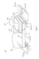
FIG.1 illustrates the structure of one embodiment of the present disclosure. -
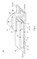
FIG.2 illustrates the structure of another embodiment of the present disclosure. -
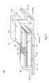
FIG.3 illustrates the structure of another embodiment of the present disclosure. -
FIG.4 illustrates the structure of another embodiment of the present disclosure. -
FIG.5 illustrates the structure of another embodiment of the present disclosure. -
FIG.6 illustrates the structure of another embodiment of the present disclosure. - The present disclosure is described by the following specific embodiments. Those with ordinary skill in the arts can readily understand the other advantages and functions of the present invention after reading the disclosure of this specification. The present disclosure can also be implemented with different embodiments. Various details described in this specification can be modified based on different viewpoints and applications without departing from the scope of the present disclosure.
- As used herein, the singular forms "a," "an" and "the" include plural referents unless the context clearly dictates otherwise. Therefore, reference to, for example, a data sequence includes aspects having two or more such sequences, unless the context clearly indicates otherwise.
- Reference will now be made in detail to the embodiments of the present disclosure, examples of which are illustrated in the accompanying drawings. Wherever possible, the same reference numbers are used in the drawings and the description to refer to the same or like parts.
- Referring to
Fig.1 , thesemiconductor component 100 of the present disclosure comprises alateral semiconductor device 110, avertical semiconductor device 120, and aleadframe 130. - The
lateral semiconductor device 110 has afirst side 111 and asecond side 112. As illustrated inFig.1 , thesecond side 112 refers to the upper surface of thelateral semiconductor device 110; and thefirst side 111 refers to the lower surface of thelateral semiconductor device 110. - The
lateral semiconductor device 110 also has an active region, positioned on thefirst side 111, comprising afirst electrode 113, asecond electrode 114, and acontrol electrode 115 positioned on the first side 111 (the lower surface). Thelateral semiconductor device 110 of the present disclosure can be metal-insulator-semiconductor field-effect transistor (MISFET), a metal semiconductor field effect transistor (MESFET) or a High-electron-mobility transistor (HEMT), which is made of a silicon-based semiconductor or a compound semiconductor and not limited to it. For the devices aforementioned, thefirst electrode 113 of the lateral semiconductor device is a source electrode, thesecond electrode 114 of the lateral semiconductor device is a drain electrode, and thecontrol electrode 115 of the lateral semiconductor device is a gate electrode. In one embodiment of the present disclosure, thelateral semiconductor device 110 is a HEMT device, which includes several wide bandgap material layers, such as III-V semiconductor layers. In an embodiment, the lateral semiconductor device comprises a channel layer made of GaN and a barrier layer made of AlGaN. Due to the different band gaps of the two layers, a two-dimensional electron gas (2DEG) is formed at the interface therebetween, the 2DEG serving as a conductive channel. The mobility of the electrons as well as the 2D-electron charge carrier density is very high in the two-dimensional electron gas, which is provided in an active region between thefirst electrode 113 of the lateral semiconductor device 110 (the source electrode) and thesecond electrode 115 of the lateral semiconductor device 110 (the drain electrode). - The
vertical semiconductor device 120 has afirst side 121 and asecond side 122. As illustrated inFig.1 , thesecond side 122 refers to the upper surface of thevertical semiconductor device 120; and thefirst side 121 refers to the lower surface of thevertical semiconductor device 120. - The
vertical semiconductor device 120 has asecond electrode 124 and acontrol electrode 125 positioned on the second side 122 (the upper surface), and afirst electrode 123 positioned on the first side 121 (the lower surface). Thevertical semiconductor device 120 of the present disclosure can be one of a metal-oxide-semiconductor field-effect transistor (MOSFET), but not limited to it. For a MOSFET device, thefirst electrode 123 of thevertical semiconductor device 120 is a drain electrode, thesecond electrode 124 of thevertical semiconductor device 120 is a source electrode, and thecontrol electrode 125 of thevertical semiconductor device 120 is a gate electrode. - The
leadframe 130 electrically and respectively connecting to each of thefirst electrode 113 of thelateral semiconductor device 110, thesecond electrode 114 of thelateral semiconductor device 110, thesecond electrode 124 of thevertical semiconductor device 120, thecontrol electrode 115 of thelateral semiconductor device 110, and thecontrol electrode 125 of thevertical semiconductor device 120. In one embodiment of the present disclosure, theleadframe 130 comprises a plurality of portions. As illustrated inFig. 1 , the plurality of portions includesportions portion 131 of theleadframe 130 is electrically connected to thefirst electrode 113 of thelateral semiconductor device 110; theportion 132 of theleadframe 130 is electrically connected to thesecond electrode 114 of thelateral semiconductor device 110; theportion 133 of theleadframe 130 is electrically connected to thecontrol electrode 115 of thelateral semiconductor device 110; theportion 134 of theleadframe 130 is electrically connected to thesecond electrode 124 of thevertical semiconductor device 120; and theportion 135 of theleadframe 130 is electrically connected to thecontrol electrode 125 of thevertical semiconductor device 120. It should be noticed that thefirst side 121 of thevertical semiconductor device 120 is mounted on thesecond side 112 of thelateral semiconductor device 110, and thefirst electrode 113 of thelateral semiconductor device 110 is also electrically connected to thefirst electrode 123 of thevertical semiconductor device 120. In one embodiment of the present disclosure, thefirst side 111 of thelateral semiconductor device 110 faces to theleadframe 130. - As shown in
Fig. 1 , thefirst electrode 113, thesecond electrode 114, and thecontrol electrode 115 of thelateral semiconductor device 110 are respectively flip-chip bonded to theportion 131 of theleadframe 130, theportion 132 of theleadframe 130, and theportion 133 of theleadframe 130. In other words, thefirst electrode 113, thesecond electrode 114, and thecontrol electrode 115 of thelateral semiconductor device 110 are disposed on theircorresponding portions leadframe 130. It should be noticed that all electrodes (thefirst electrode 113, thesecond electrode 114, and the control electrode 115) of thelateral semiconductor device 110 of the present disclosure can be bonded to their corresponding leadframe in a single step, flip-chip bonding, since these electrode are positioned on the same side of thelateral semiconductor device 110. - As illustrated in
Fig.1 , the bonding-wires 192 connect thesecond electrode 124 of thevertical semiconductor device 120 to theportion 134 of theleadframe 130, thecontrol electrode 125 of thevertical semiconductor device 120 to theportion 135 of theleadframe 130, and thefirst electrode 113 of thelateral semiconductor device 110 to thefirst electrode 123 of thevertical semiconductor device 120. It should be noticed that one of the bonding-wire 192 is both electrically connected to thefirst electrode 113 of thelateral semiconductor device 110 and thefirst electrode 123 of thevertical semiconductor device 120. Therefore, thelateral semiconductor device 110 and thevertical semiconductor device 120 are not only packaged in one stacked structure. More importantly, a series connection of thelateral semiconductor device 110 and thevertical semiconductor device 120 are formed since thefirst electrode 113 of thelateral semiconductor device 110 and thefirst electrode 123 ofvertical semiconductor device 120 are electrically connected. In one embodiment of the present disclosure, the bonding-wire 192 comprises one of the gold, gold alloy, aluminum, an aluminum alloy, copper and a copper alloy. - In one embodiment of the present disclosure, the
first electrode 113 of thelateral semiconductor device 110 is a source electrode, thesecond electrode 114 of thelateral semiconductor device 110 is a drain electrode, and thecontrol electrode 125 is a gate electrode of thelateral semiconductor device 110; thefirst electrode 123 of thevertical semiconductor device 120 is a drain electrode, thesecond electrode 124 of thevertical semiconductor device 120 is a source electrode, and thecontrol electrode 125 is a gate electrode of thevertical semiconductor device 120, so as to the current flow within thesemiconductor component 100 flows in theportion 132 of theleadframe 130 to thesecond electrode 114 of thelateral semiconductor device 110, thefirst electrode 113 of thelateral semiconductor device 110, theportion 131 of theleadframe 130, thefirst electrode 123 of thevertical semiconductor device 120, thesecond electrode 124 of thevertical semiconductor device 120, and finally flows out from theportion 134 of theleadframe 130. Thecontrol electrode 125 of thevertical semiconductor device 120 is a switch to turn on/off the current between thefirst electrode 123 of thevertical semiconductor device 120 and thesecond electrode 124 of thevertical semiconductor device 120 by inputting signal to theportion 135 of theleadframe 130; and thecontrol electrode 115 of thelateral semiconductor device 110 is a switch to turn on/off the current between thesecond electrode 114 of thelateral semiconductor device 110 and thefirst electrode 113 of thelateral semiconductor device 110 by inputting signal to theportion 133 of theleadframe 130. In one embodiment, theportion 134 of theleadframe 130 is electrically connected to theportion 133 of theleadframe 130. In other words, thesecond electrode 124 of thevertical semiconductor device 120 is electrically connected to thecontrol electrode 115 of thelateral semiconductor device 110. - In another embodiment of the present disclosure, the
first electrode 113 of thelateral semiconductor device 110 is a drain electrode, thesecond electrode 114 of thelateral semiconductor device 110 is a source electrode, and thecontrol electrode 125 is a gate electrode of thelateral semiconductor device 110; thethird electrode 123 is a source electrode, thesecond electrode 124 of thevertical semiconductor device 120 is a drain electrode, and thecontrol electrode 125 is a gate electrode of thevertical semiconductor device 120, so as to the current flow within thesemiconductor component 100 flows in theportion 134 of theleadframe 130 to thesecond electrode 124 of thevertical semiconductor device 120, thefirst electrode 123 of thevertical semiconductor device 120, theportion 131 of theleadframe 130, thefirst electrode 113 of thelateral semiconductor device 110, thesecond electrode 114 of thelateral semiconductor device 110, and finally flows out from theportion 132leadframe 130. Similarly, thecontrol electrode 125 of thevertical semiconductor device 120 is a switch to turn on/off the current between thesecond electrode 124 of thevertical semiconductor device 120 and thefirst electrode 123 of thevertical semiconductor device 120 by inputting signal to theportion 135 of theleadframe 130; and thecontrol electrode 115 of thelateral semiconductor device 110 is a switch to turn on/off the current between thefirst electrode 113 of thelateral semiconductor device 110 and thesecond electrode 114 of thelateral semiconductor device 110 by inputting signal to theportion 133 of theleadframe 130. - In one embodiment of the present disclosure, at least two of the plurality of portions are substantially coplanar. As illustrated in
Fig.1 , allprotions semiconductor component 100 can be simply performed by single-side bonding thesemiconductor component 100 to. However, in another embodiment of the present disclosure, at least two of the plurality of portions are substantially non-coplanar. The positions of the protions of theleadframe 130 can be altered in different designs, coplanar or non-coplanar, to varieties of needs. As shown inFig. 1 , in one embodiment of the present disclosure, theportion 131 of theleadframe 130, theportion 132 of theleadframe 130, and theportions 133 of theleadframe 130, which are respectively flip-chip bonded to thefirst electrode 113, thesecond electrode 114, and thecontrol electrode 115 of thelateral semiconductor device 110, are coplanar (since thefirst electrode 113, thesecond electrode 114, and thecontrol electrode 115 are all positioned on thefirst side 111 of the lateral semiconductor device 110). The electrically connections between two elements which are positioned on different height levels, such as theportion 134 of theleadframe 130 to thesecond electrode 124 of thevertical semiconductor device 120, theportion 135 of theleadframe 130 to thecontrol electrode 125 of thevertical semiconductor device 120, and theportion 131 of theleadframe 130 to thefirst electrode 123 of the vertical semiconductor device 120) are formed by connecting aforementioned elements with bonding-wires 192. - However, bonding-
wire 192 is not the only option to electrically connect the elements which are positioned on different height levels. In one embodiment of the present disclosure, further comprising afirst connector 160 electrically connecting thefirst electrode 113 of thelateral semiconductor device 110 and thefirst electrode 123 of thevertical semiconductor device 120. In another embodiment of the present disclosure, further comprising asecond connector 180 contacts both thesecond electrode 124 of thevertical semiconductor 120 and theleadframe 130. As illustrated inFig.2 , the electrically connection between theportion 131 of the leadframe 130and thefirst electrode 123 of thevertical semiconductor device 120, and the electrically connection between theportion 134 of theleadframe 130 and thesecond electrode 124 of thevertical semiconductor device 120 can be formed by applying thefirst connector 160 and thesecond connector 180 respectively. In one embodiment of the present disclosure, thefirst connector 160 comprises a clip, ribbon, or bonding-wire. In another embodiment of the present disclosure, thesecond connector 180 comprises a clip, ribbon, or bonding-wire. As illustrated inFig.2 , thefirst connector 160 is a metal clip connects both theportion 131 of theleadframe 130 and thefirst electrode 123 of thevertical semiconductor device 120, such that thefirst electrode 113 of thelateral semiconductor device 110 is electrically connected to thefirst electrode 123 of thevertical semiconductor device 120 to form the series connection of thelateral semiconductor device 110 and thevertical semiconductor device 120. - Also illustrated in
Fig.2 , thesecond connector 180 is a metal clip connects both theportion 134 of theleadframe 130 and thesecond electrode 124 of thevertical semiconductor device 120, such that the signal input/output of thesemiconductor component 200 can be performed. It should be noticed that since the metal clips has wider cross-section than that of the bonding-wires 192, therefore the capability to carrying current flow of the metal clips is much better than that of the bonding-wires 192. Accordingly, thesemiconductor component 200 illustrated inFig. 2 has better capability to be operated in high current flow than that of thesemiconductor component 100 illustrated inFig. 1 . In addition, the metal clips also have wide surfaces which help diffuse the heat, which is generated in component operation, from thesemiconductor component 200 to its surrounding. If a device is over-heated by its heat accumulation, damages of the device are expected. The heat accumulation is more serious while the device is operated in high current flow. Accordingly, thesemiconductor component 200 illustrated inFig. 2 has better reliability to be operated in high current flow than that of thesemiconductor component 100 illustrated inFig. 1 . In one embodiment of the present disclosure, the metal clipmay include a material selected from the group of , Ni, Al, Cu, Ag, Au and alloy thereof. - As illustrated in
Fig. 3 , in one embodiment of the present disclosure, thecontrol electrode 115 of thelateral semiconductor device 110 is electrically connected to thefirst electrode 123 of the vertical semiconductor device120. For example, thefirst electrode 113 and thecontrol electrode 115 of thelateral semiconductor device 110 have flip-chip contacts to thecommon portion 131 of theleadframe 130. In other words, thecontrol electrode 115 of thelateral semiconductor device 110 does not need to be controlled independently, and itscorresponding portion 133 of theleadframe 130, as illustrated inFig. 1 andFig. 2 , can be further eliminated. In one embodiment of the present disclosure, thefirst electrode 113 of thelateral semiconductor device 110 is a source electrode, thesecond electrode 114 of thelateral semiconductor device 110 is a drain electrode, and thecontrol electrode 125 is a gate electrode of thelateral semiconductor device 110; thefirst electrode 123 of thevertical semiconductor device 120 is a drain electrode, thesecond electrode 124 of thevertical semiconductor device 120 is a source electrode, and thecontrol electrode 125 is a gate electrode of thevertical semiconductor device 120, so as to the current flow within thesemiconductor component 300 flows in theportion 132 of theleadframe 130 to thesecond electrode 114 of thelateral semiconductor device 110, thefirst electrode 113 of thelateral semiconductor device 110, theportion 131 of theleadframe 130, thefirst electrode 123 of thevertical semiconductor device 120, thesecond electrode 124 of thevertical semiconductor device 120, and finally flows out from theportion 134leadframe 130. Thecontrol electrode 125 of thevertical semiconductor device 120 is a switch to turn on/off the current between thefirst electrode 123 and thesecond electrode 124 of the vertical semiconductor device 120by inputting signal to theportion 135 of theleadframe 130, however, thelateral semiconductor device 110, which is in series connection (also cascode connection) with thevertical semiconductor device 120, does not need to be controlled independently. To be more specific, when theportion 131 of theleadframe 130 receives the current flow from thesecond electrode 114 of thelateral semiconductor device 110, the current flow subsequently flows to both thefirst electrode 113 of the lateral semiconductor device 110 (source electrode) and thecontrol electrode 115 of the lateral semiconductor device 110 (gate electrode) simultaneously. Therefore, thelateral semiconductor device 110 is automatically turning on whilevertical semiconductor device 120 is turning on and the current flow flows in itsfirst electrode 113 of the lateral semiconductor device 110 (source electrode) since the current flow also flows in itscontrol electrode 115 of the lateral semiconductor device 110 (gate electrode) in the same time. In this case, thesemiconductor component 300 substantially possesses only one control electrode 125 (gate electrode), positioned on thesecond side 122 of thevertical semiconductor device 120, to control the series connection (also cascode connection) of thelateral semiconductor device 110 and thevertical semiconductor device 120. In general, the selection of thevertical semiconductor device 120 is usually fast switching than that of thelateral semiconductor 110. In one embodiment of the present disclosure, thelateral semiconductor device 110 has a thickness larger than that of thevertical semiconductor device 120. Therefore thevertical semiconductor device 120 has faster response to driving signals flow in its control electrode 125(gate) than that of thelateral semiconductor device 110. Accordingly, on/off controlling of thesemiconductor component 300 is easier and faster since thesemiconductor component 300 has a simpler design than that of thesemiconductor components - In another embodiment of the present disclosure, the
semiconductor 300 further comprises apassivation layer 150 positioned on thefirst side 111 of thelateral semiconductor device 110. As illustrated inFig. 3 , thepassivation layer 150 is positioned on thefirst side 111 to cover and protect the active area of thelateral semiconductor device 110. The active area includes the current channel between thefirst electrode 113 and thesecond electrode 114. Thepassivation layer 150 covers the active area so that the active area is not directly exposed to air or moisture from surrounding, and the lifetime of thelateral semiconductor device 110 is extended. Thepassivation layer 150 may include a material selected from the group of SixNy, SiO2 and Al2O3. - In one embodiment of the present disclosure, as illustrated in
Fig. 3 , thepassivation layer 150 contacts theportion 131 of theleadframe 130 which have the flip-chip contacts to both thefirst electrode 113 and thecontrol electrode 115 of thelateral semiconductor device 110. Thepassivation layer 150 receives the heat generated in the active area of thelateral semiconductor device 110 and further diffuses the heat to theportion 131 of theleadframe 130. It reduces the heat accumulation, and increases the reliability of thesemiconductor component 300. - In another embodiment of the present disclosure as illustrated in
Fig. 4 , thepassivation layer 150 contacts theportion 132 of the leadframe 130which have the flip-chip contact to thesecond electrode 114 of thelateral semiconductor device 110. Thepassivation layer 150 also receives the heat generated in the active area of thelateral semiconductor device 110 and further diffuses the heat to theportion 132 of theleadframe 130. Similarly, the heat accumulation of thesemiconductor module 400 is reduced, and reliability of thesemiconductor module 400 is improved. - As illustrated in
Fig. 5 , in one embodiment of the present disclosure, thesemiconductor component 500 further comprises aconductive layer 170 on the second side of thelateral semiconductor device 110, wherein thefirst electrode 123 of thevertical semiconductor device 120 contacts theconductive layer 170, and thefirst connector 160 contacts both thefirst electrode 113 of thelateral semiconductor device 110 and theconductive layer 170. That is, thefirst connector 160 does not contact thefirst electrode 123 of thevertical semiconductor device 120 directly, but contacts theconductive layer 170 which contacts thefirst electrode 125 of thevertical semiconductor device 120. Therefore, the electrical connection of thefirst electrode 123 of thevertical semiconductor device 120 and thefirst electrode 113 of thelateral semiconductor device 110 is also established as the previous embodiments. - In one embodiment of the present disclosure as shown in
Fig. 6 , thesemiconductor component 600 further comprising athird connector 190 contacts both thecontrol electrode 125 of thevertical semiconductor device 120 and theportion 135 of theleadframe 130, and the electrical connection of thecontrol electrode 125 of thevertical semiconductor device 120 and itscorresponding portion 135 of theleadframe 130 is also established as the previous embodiments. - Although the present disclosure has been described in considerable detail with reference to certain embodiments thereof, other embodiments are possible. Therefore, the spirit and scope of the appended claims should not be limited to the description of the embodiments contained herein.
- It will be apparent to those ordinarily skilled in the art that various modifications and variations may be made to the structure of the present disclosure without departing from the scope or spirit of the disclosure. In view of the foregoing, it is intended that the present disclosure cover modifications and variations thereof provided they fall within the scope of the following claims.
Claims (19)
- A semiconductor component comprising:a lateral semiconductor device having a first side and a second side, the lateral semiconductor device having an active region, positioned on the first side, comprising a first electrode, a second electrode, and a control electrode;a vertical semiconductor device having a first side and a second side, the vertical semiconductor device comprising a first electrode positioned on the first side and a second electrode and a control electrode positioned on the second side; anda leadframe electrically and respectively connected to each of the first electrode of the lateral semiconductor device, the second electrode of the lateral semiconductor device, the second electrode of the vertical semiconductor device, and the control electrodes,wherein the first side of the vertical semiconductor device is mounted on the second side of the lateral semiconductor device, and wherein the first electrode of the lateral semiconductor device is also electrically connected to the first electrode of the vertical semiconductor device.
- The semiconductor component according to claim 1, wherein the first side of the lateral semiconductor device faces to the leadframe.
- The semiconductor component according to claim 1, wherein the control electrode of the lateral semiconductor device is electrically connected to the first electrode of the vertical semiconductor device.
- The semiconductor component according to claim 3, further comprising a passivation layer positioned on the first side of the lateral semiconductor device.
- The semiconductor component according to claim 1, wherein the leadframe comprises a plurality of portions.
- The semiconductor component according to claim 5, wherein at least two of the plurality of portions are substantially coplanar.
- The semiconductor component according to claim 5, wherein at least two of the plurality of portions are substantially non-coplanar.
- The semiconductor component according to claim 1, further comprising a first connector electrically connecting the first electrode of the lateral semiconductor device and the first electrode of the vertical semiconductor device.
- The semiconductor component according to claim 8, further comprising a conductive layer on the second side of the lateral semiconductor device, wherein the first electrode of the vertical semiconductor device contacts the conductive layer, and the first connector electrically connects the first electrode of the lateral semiconductor device and the conductive layer.
- The semiconductor component according to claim 8, wherein the first connector comprises a clip, ribbon, or bonding-wire.
- The semiconductor component according to claim 1, further comprising a second connector contacts both the second electrode of the vertical semiconductor and the leadframe.
- The semiconductor component according to claim 11, wherein the second connector comprises a clip, ribbon, or bonding-wire.
- The semiconductor component according to claim 1, further comprising a third connector contacts both the control electrode of the vertical semiconductor device and the leadframe.
- The semiconductor component according to claim 13, wherein the third connector comprises a clip, ribbon, or bonding-wire.
- The semiconductor component according to claim 1, wherein the lateral semiconductor device comprises a metal-insulator-semiconductor field-effect transistor (MISFET), a metal semiconductor field effect transistor (MESFET), or a High-electron-mobility transistor (HEMT).
- The semiconductor component according to claim 1, wherein the lateral semiconductor device comprises a nitride-based power transistor.
- The semiconductor component according to claim 1, wherein the first electrode of the lateral semiconductor device is a source electrode, the second electrode of the lateral semiconductor device is a drain electrode, the first electrode of the vertical semiconductor device is a drain electrode, the second electrode of the vertical semiconductor device is a source electrode, and the control electrodes of the lateral and the vertical semiconductor devices are gate electrodes.
- The semiconductor component according to claim 1, wherein the lateral semiconductor device has a thickness larger than that of the vertical semiconductor device.
- The semiconductor component according to claim 1, wherein the control electrode of the lateral semiconductor device is electrically connected to the second electrode of the vertical semiconductor device.
Applications Claiming Priority (1)
| Application Number | Priority Date | Filing Date | Title |
|---|---|---|---|
| US13/930,817 US9385070B2 (en) | 2013-06-28 | 2013-06-28 | Semiconductor component having a lateral semiconductor device and a vertical semiconductor device |
Publications (3)
| Publication Number | Publication Date |
|---|---|
| EP2840605A2 true EP2840605A2 (en) | 2015-02-25 |
| EP2840605A3 EP2840605A3 (en) | 2015-03-04 |
| EP2840605B1 EP2840605B1 (en) | 2017-08-09 |
Family
ID=49115444
Family Applications (1)
| Application Number | Title | Priority Date | Filing Date |
|---|---|---|---|
| EP13183554.8A Not-in-force EP2840605B1 (en) | 2013-06-28 | 2013-09-09 | A semiconductor component having a lateral semiconductor device and a vertical semiconductor device |
Country Status (5)
| Country | Link |
|---|---|
| US (1) | US9385070B2 (en) |
| EP (1) | EP2840605B1 (en) |
| CN (1) | CN104253156B (en) |
| NO (1) | NO2923169T3 (en) |
| TW (1) | TWI560814B (en) |
Families Citing this family (20)
| Publication number | Priority date | Publication date | Assignee | Title |
|---|---|---|---|---|
| KR101977994B1 (en) * | 2013-06-28 | 2019-08-29 | 매그나칩 반도체 유한회사 | Semiconductor pacakge |
| US9245831B1 (en) * | 2014-11-05 | 2016-01-26 | Alpha And Omega Semiconductor (Cayman) Ltd. | Top-exposed semiconductor package and the manufacturing method |
| US9379193B2 (en) | 2014-08-07 | 2016-06-28 | Semiconductor Components Industries, Llc | Semiconductor package for a lateral device and related methods |
| US9589868B2 (en) * | 2015-03-11 | 2017-03-07 | Gan Systems Inc. | Packaging solutions for devices and systems comprising lateral GaN power transistors |
| DE102015012915B4 (en) * | 2015-10-06 | 2020-10-15 | Audi Ag | Arrangement of semiconductor elements on a semiconductor module for a power module or a corresponding method |
| US10892210B2 (en) | 2016-10-03 | 2021-01-12 | Delta Electronics, Inc. | Package structures |
| KR101954393B1 (en) * | 2017-02-20 | 2019-03-05 | 신덴겐코교 가부시키가이샤 | Electronic device |
| CN107086215A (en) * | 2017-05-26 | 2017-08-22 | 厦门市东太耀光电子有限公司 | A kind of LED based on front pad can eutectic encapsulating structure and method |
| JP7437582B2 (en) * | 2018-04-11 | 2024-02-26 | ヒタチ・エナジー・リミテッド | Material reduction metal plate on power semiconductor chip |
| US10580762B1 (en) * | 2018-10-25 | 2020-03-03 | Infineon Technologies Ag | Integrated circuit (IC) chip arrangement |
| EP3703123B1 (en) | 2019-02-27 | 2024-08-14 | Infineon Technologies Austria AG | Semiconductor component and semiconductor package |
| TWI726313B (en) | 2019-04-30 | 2021-05-01 | 作同 柯 | Power semiconductor |
| EP3739756A1 (en) * | 2019-05-17 | 2020-11-18 | Nexperia B.V. | Cascode semiconductor device and method of manufacture |
| US11355470B2 (en) * | 2020-02-27 | 2022-06-07 | Amkor Technology Singapore Holding Pte. Ltd. | Semiconductor device and methods of manufacturing semiconductor devices |
| CN111370496B (en) | 2020-03-18 | 2021-10-26 | 京东方科技集团股份有限公司 | Thin film transistor, manufacturing method thereof and display device |
| EP3882969B1 (en) * | 2020-03-18 | 2024-05-01 | Nexperia B.V. | A cascode semiconductor device and method of manufacture |
| US11342248B2 (en) | 2020-07-14 | 2022-05-24 | Gan Systems Inc. | Embedded die packaging for power semiconductor devices |
| US11211373B1 (en) * | 2021-02-22 | 2021-12-28 | United Silicon Carbide, Inc. | Double-sided chip stack assembly |
| JP7770282B2 (en) * | 2022-10-21 | 2025-11-14 | 三菱電機株式会社 | Semiconductor device, power conversion device, and method of manufacturing the semiconductor device |
| CN116913911B (en) * | 2023-09-05 | 2023-12-22 | 深圳智芯微电子科技有限公司 | Cascaded GaN HEMT packaging device and preparation method thereof |
Citations (2)
| Publication number | Priority date | Publication date | Assignee | Title |
|---|---|---|---|---|
| US5192987A (en) | 1991-05-17 | 1993-03-09 | Apa Optics, Inc. | High electron mobility transistor with GaN/Alx Ga1-x N heterojunctions |
| US6849882B2 (en) | 2001-05-11 | 2005-02-01 | Cree Inc. | Group-III nitride based high electron mobility transistor (HEMT) with barrier/spacer layer |
Family Cites Families (44)
| Publication number | Priority date | Publication date | Assignee | Title |
|---|---|---|---|---|
| US6448110B1 (en) * | 1999-08-25 | 2002-09-10 | Vanguard International Semiconductor Corporation | Method for fabricating a dual-chip package and package formed |
| JP2005011986A (en) * | 2003-06-19 | 2005-01-13 | Sanyo Electric Co Ltd | Semiconductor device |
| US7074647B2 (en) * | 2003-07-07 | 2006-07-11 | Freescale Semiconductor, Inc. | Semiconductor component comprising leadframe, semiconductor chip and integrated passive component in vertical relationship to each other |
| JP2005302951A (en) * | 2004-04-09 | 2005-10-27 | Toshiba Corp | Power semiconductor device package |
| JP2006216940A (en) | 2005-01-07 | 2006-08-17 | Toshiba Corp | Semiconductor device |
| US7443014B2 (en) * | 2005-10-25 | 2008-10-28 | Infineon Technologies Ag | Electronic module and method of assembling the same |
| DE102005055761B4 (en) * | 2005-11-21 | 2008-02-07 | Infineon Technologies Ag | Power semiconductor component with semiconductor chip stack in bridge circuit and method for producing the same |
| US7291869B2 (en) * | 2006-02-06 | 2007-11-06 | Infieon Technologies A.G. | Electronic module with stacked semiconductors |
| JP5598787B2 (en) | 2006-04-17 | 2014-10-01 | マイクロンメモリジャパン株式会社 | Manufacturing method of stacked semiconductor device |
| US7569920B2 (en) * | 2006-05-10 | 2009-08-04 | Infineon Technologies Ag | Electronic component having at least one vertical semiconductor power transistor |
| DE102006021959B4 (en) * | 2006-05-10 | 2011-12-29 | Infineon Technologies Ag | Power semiconductor device and method for its production |
| US7271470B1 (en) * | 2006-05-31 | 2007-09-18 | Infineon Technologies Ag | Electronic component having at least two semiconductor power devices |
| DE102006031405B4 (en) * | 2006-07-05 | 2019-10-17 | Infineon Technologies Ag | Semiconductor module with switching functions and method of making the same |
| DE102006034679A1 (en) * | 2006-07-24 | 2008-01-31 | Infineon Technologies Ag | Semiconductor module with power semiconductor chip and passive component and method for producing the same |
| US7825508B2 (en) * | 2006-07-28 | 2010-11-02 | Alpha Omega Semiconductor, Inc. | Multi-die DC-DC buck power converter with efficient packaging |
| DE102007012154B4 (en) * | 2007-03-12 | 2014-05-08 | Infineon Technologies Ag | Semiconductor module with semiconductor chips and method for producing the same |
| DE102007018914B4 (en) * | 2007-04-19 | 2019-01-17 | Infineon Technologies Ag | Semiconductor device with a semiconductor chip stack and method for producing the same |
| US7884452B2 (en) * | 2007-11-23 | 2011-02-08 | Alpha And Omega Semiconductor Incorporated | Semiconductor power device package having a lead frame-based integrated inductor |
| US7825502B2 (en) | 2008-01-09 | 2010-11-02 | Fairchild Semiconductor Corporation | Semiconductor die packages having overlapping dice, system using the same, and methods of making the same |
| US20090261462A1 (en) | 2008-04-16 | 2009-10-22 | Jocel Gomez | Semiconductor package with stacked die assembly |
| US8240029B2 (en) * | 2008-11-20 | 2012-08-14 | Powertech Technology Inc. | Method for forming an isolated inner lead from a leadframe |
| CN101662562B (en) * | 2009-09-12 | 2011-09-14 | 苏州佳世达电通有限公司 | Feed-in film scanning correction method |
| US20120326287A1 (en) * | 2011-06-27 | 2012-12-27 | National Semiconductor Corporation | Dc/dc convertor power module package incorporating a stacked controller and construction methodology |
| US8581376B2 (en) * | 2010-03-18 | 2013-11-12 | Alpha & Omega Semiconductor Incorporated | Stacked dual chip package and method of fabrication |
| US9214417B2 (en) * | 2010-06-18 | 2015-12-15 | Alpha And Omega Semiconductor Incorporated | Combined packaged power semiconductor device |
| JP2012015202A (en) * | 2010-06-29 | 2012-01-19 | On Semiconductor Trading Ltd | Semiconductor device, and method of manufacturing the same |
| US8896107B2 (en) * | 2011-01-03 | 2014-11-25 | International Rectifier Corporation | High power semiconductor package with conductive clip |
| US8426952B2 (en) | 2011-01-14 | 2013-04-23 | International Rectifier Corporation | Stacked half-bridge package with a common conductive leadframe |
| JP5813963B2 (en) * | 2011-02-28 | 2015-11-17 | ローム株式会社 | Semiconductor device and mounting structure of semiconductor device |
| US9842797B2 (en) * | 2011-03-07 | 2017-12-12 | Texas Instruments Incorporated | Stacked die power converter |
| US20120228696A1 (en) * | 2011-03-07 | 2012-09-13 | Texas Instruments Incorporated | Stacked die power converter |
| US8742490B2 (en) * | 2011-05-02 | 2014-06-03 | Monolithic Power Systems, Inc. | Vertical power transistor die packages and associated methods of manufacturing |
| CN102903692B (en) * | 2011-07-26 | 2015-05-27 | 万国半导体股份有限公司 | Stacked power semiconductor device with double-layer lead frame and production method thereof |
| US8643176B2 (en) * | 2011-07-27 | 2014-02-04 | Infineon Technologies Ag | Power semiconductor chip having two metal layers on one face |
| US9524957B2 (en) | 2011-08-17 | 2016-12-20 | Intersil Americas LLC | Back-to-back stacked dies |
| JP5924110B2 (en) * | 2012-05-11 | 2016-05-25 | 株式会社ソシオネクスト | Semiconductor device, semiconductor device module, and semiconductor device manufacturing method |
| US9036442B2 (en) * | 2012-06-29 | 2015-05-19 | Intersil Americas LLC | Reduced-noise reference voltage platform for a voltage converter device |
| US9018744B2 (en) * | 2012-09-25 | 2015-04-28 | Infineon Technologies Ag | Semiconductor device having a clip contact |
| US20140175628A1 (en) * | 2012-12-21 | 2014-06-26 | Hua Pan | Copper wire bonding structure in semiconductor device and fabrication method thereof |
| US9966330B2 (en) * | 2013-03-14 | 2018-05-08 | Vishay-Siliconix | Stack die package |
| US9589929B2 (en) * | 2013-03-14 | 2017-03-07 | Vishay-Siliconix | Method for fabricating stack die package |
| US9054091B2 (en) * | 2013-06-10 | 2015-06-09 | Alpha & Omega Semiconductor, Inc. | Hybrid packaged lead frame based multi-chip semiconductor device with multiple semiconductor chips and multiple interconnecting structures |
| US9437587B2 (en) * | 2014-01-19 | 2016-09-06 | Alpha & Omega Semiconductor, Inc. | Flip chip semiconductor device |
| US9735078B2 (en) * | 2014-04-16 | 2017-08-15 | Infineon Technologies Ag | Device including multiple semiconductor chips and multiple carriers |
-
2013
- 2013-06-28 US US13/930,817 patent/US9385070B2/en active Active - Reinstated
- 2013-09-06 TW TW102132088A patent/TWI560814B/en not_active IP Right Cessation
- 2013-09-09 EP EP13183554.8A patent/EP2840605B1/en not_active Not-in-force
- 2013-09-11 CN CN201310412957.2A patent/CN104253156B/en not_active Expired - Fee Related
- 2013-11-18 NO NO13792016A patent/NO2923169T3/no unknown
Patent Citations (2)
| Publication number | Priority date | Publication date | Assignee | Title |
|---|---|---|---|---|
| US5192987A (en) | 1991-05-17 | 1993-03-09 | Apa Optics, Inc. | High electron mobility transistor with GaN/Alx Ga1-x N heterojunctions |
| US6849882B2 (en) | 2001-05-11 | 2005-02-01 | Cree Inc. | Group-III nitride based high electron mobility transistor (HEMT) with barrier/spacer layer |
Also Published As
| Publication number | Publication date |
|---|---|
| EP2840605A3 (en) | 2015-03-04 |
| CN104253156B (en) | 2017-10-27 |
| TW201501246A (en) | 2015-01-01 |
| NO2923169T3 (en) | 2018-02-24 |
| US20150001692A1 (en) | 2015-01-01 |
| CN104253156A (en) | 2014-12-31 |
| EP2840605B1 (en) | 2017-08-09 |
| US9385070B2 (en) | 2016-07-05 |
| TWI560814B (en) | 2016-12-01 |
Similar Documents
| Publication | Publication Date | Title |
|---|---|---|
| US9385070B2 (en) | Semiconductor component having a lateral semiconductor device and a vertical semiconductor device | |
| US10950524B2 (en) | Heterojunction semiconductor device for reducing parasitic capacitance | |
| KR101539531B1 (en) | Semiconductor device | |
| CN103824845B (en) | Semiconductor device with a plurality of semiconductor chips | |
| US10290566B2 (en) | Electronic component | |
| US9654001B2 (en) | Semiconductor device | |
| US8981380B2 (en) | Monolithic integration of silicon and group III-V devices | |
| EP3007227B1 (en) | Compact power semiconductor package | |
| JP5728258B2 (en) | Semiconductor device | |
| US10032736B2 (en) | Semiconductor device | |
| JP2006351691A (en) | Semiconductor device | |
| US20170352753A1 (en) | Field-effect transistor | |
| US10833185B2 (en) | Heterojunction semiconductor device having source and drain pads with improved current crowding | |
| US20160204099A1 (en) | Semiconductor device and method of manufacturing the same | |
| EP4629777A2 (en) | Nitride-based semiconductor bidirectional switching device and method for manufacturing the same | |
| US9324819B1 (en) | Semiconductor device | |
| JP2021531655A (en) | Monolithic microwave integrated circuit with both enhancement mode and depletion mode transistors | |
| US20240055330A1 (en) | Semiconductor device package | |
| US20240379835A1 (en) | Semiconductor device and semiconductor module | |
| US20240136434A1 (en) | Nitride semiconductor element and nitride semiconductor device | |
| WO2024011439A1 (en) | Semiconductor packaged device and method for manufacturing the same | |
| CN117916879A (en) | Semiconductor packaging device and manufacturing method thereof | |
| CN118511288A (en) | Semiconductor package device and method of manufacturing the same | |
| CN117578656A (en) | Circuit systems, methods for operating circuit systems |
Legal Events
| Date | Code | Title | Description |
|---|---|---|---|
| PUAL | Search report despatched |
Free format text: ORIGINAL CODE: 0009013 |
|
| PUAI | Public reference made under article 153(3) epc to a published international application that has entered the european phase |
Free format text: ORIGINAL CODE: 0009012 |
|
| 17P | Request for examination filed |
Effective date: 20130909 |
|
| AK | Designated contracting states |
Kind code of ref document: A2 Designated state(s): AL AT BE BG CH CY CZ DE DK EE ES FI FR GB GR HR HU IE IS IT LI LT LU LV MC MK MT NL NO PL PT RO RS SE SI SK SM TR |
|
| AX | Request for extension of the european patent |
Extension state: BA ME |
|
| AK | Designated contracting states |
Kind code of ref document: A3 Designated state(s): AL AT BE BG CH CY CZ DE DK EE ES FI FR GB GR HR HU IE IS IT LI LT LU LV MC MK MT NL NO PL PT RO RS SE SI SK SM TR |
|
| AX | Request for extension of the european patent |
Extension state: BA ME |
|
| RIC1 | Information provided on ipc code assigned before grant |
Ipc: H01L 23/495 20060101AFI20150123BHEP Ipc: H01L 23/31 20060101ALN20150123BHEP |
|
| RBV | Designated contracting states (corrected) |
Designated state(s): AL AT BE BG CH CY CZ DE DK EE ES FI FR GB GR HR HU IE IS IT LI LT LU LV MC MK MT NL NO PL PT RO RS SE SI SK SM TR |
|
| 17Q | First examination report despatched |
Effective date: 20160229 |
|
| STAA | Information on the status of an ep patent application or granted ep patent |
Free format text: STATUS: EXAMINATION IS IN PROGRESS |
|
| GRAP | Despatch of communication of intention to grant a patent |
Free format text: ORIGINAL CODE: EPIDOSNIGR1 |
|
| STAA | Information on the status of an ep patent application or granted ep patent |
Free format text: STATUS: GRANT OF PATENT IS INTENDED |
|
| RIC1 | Information provided on ipc code assigned before grant |
Ipc: H01L 23/31 20060101ALN20170214BHEP Ipc: H01L 23/495 20060101AFI20170214BHEP |
|
| INTG | Intention to grant announced |
Effective date: 20170301 |
|
| GRAS | Grant fee paid |
Free format text: ORIGINAL CODE: EPIDOSNIGR3 |
|
| GRAA | (expected) grant |
Free format text: ORIGINAL CODE: 0009210 |
|
| STAA | Information on the status of an ep patent application or granted ep patent |
Free format text: STATUS: THE PATENT HAS BEEN GRANTED |
|
| RAP1 | Party data changed (applicant data changed or rights of an application transferred) |
Owner name: DELTA ELECTRONICS, INC. |
|
| AK | Designated contracting states |
Kind code of ref document: B1 Designated state(s): AL AT BE BG CH CY CZ DE DK EE ES FI FR GB GR HR HU IE IS IT LI LT LU LV MC MK MT NL NO PL PT RO RS SE SI SK SM TR |
|
| REG | Reference to a national code |
Ref country code: GB Ref legal event code: FG4D |
|
| REG | Reference to a national code |
Ref country code: CH Ref legal event code: EP Ref country code: AT Ref legal event code: REF Ref document number: 917685 Country of ref document: AT Kind code of ref document: T Effective date: 20170815 |
|
| REG | Reference to a national code |
Ref country code: IE Ref legal event code: FG4D |
|
| REG | Reference to a national code |
Ref country code: DE Ref legal event code: R096 Ref document number: 602013024671 Country of ref document: DE |
|
| REG | Reference to a national code |
Ref country code: FR Ref legal event code: PLFP Year of fee payment: 5 |
|
| REG | Reference to a national code |
Ref country code: NL Ref legal event code: MP Effective date: 20170809 |
|
| REG | Reference to a national code |
Ref country code: LT Ref legal event code: MG4D |
|
| REG | Reference to a national code |
Ref country code: AT Ref legal event code: MK05 Ref document number: 917685 Country of ref document: AT Kind code of ref document: T Effective date: 20170809 |
|
| REG | Reference to a national code |
Ref country code: NO Ref legal event code: T2 Effective date: 20170809 |
|
| PG25 | Lapsed in a contracting state [announced via postgrant information from national office to epo] |
Ref country code: AT Free format text: LAPSE BECAUSE OF FAILURE TO SUBMIT A TRANSLATION OF THE DESCRIPTION OR TO PAY THE FEE WITHIN THE PRESCRIBED TIME-LIMIT Effective date: 20170809 Ref country code: SE Free format text: LAPSE BECAUSE OF FAILURE TO SUBMIT A TRANSLATION OF THE DESCRIPTION OR TO PAY THE FEE WITHIN THE PRESCRIBED TIME-LIMIT Effective date: 20170809 Ref country code: FI Free format text: LAPSE BECAUSE OF FAILURE TO SUBMIT A TRANSLATION OF THE DESCRIPTION OR TO PAY THE FEE WITHIN THE PRESCRIBED TIME-LIMIT Effective date: 20170809 Ref country code: HR Free format text: LAPSE BECAUSE OF FAILURE TO SUBMIT A TRANSLATION OF THE DESCRIPTION OR TO PAY THE FEE WITHIN THE PRESCRIBED TIME-LIMIT Effective date: 20170809 Ref country code: LT Free format text: LAPSE BECAUSE OF FAILURE TO SUBMIT A TRANSLATION OF THE DESCRIPTION OR TO PAY THE FEE WITHIN THE PRESCRIBED TIME-LIMIT Effective date: 20170809 Ref country code: NL Free format text: LAPSE BECAUSE OF FAILURE TO SUBMIT A TRANSLATION OF THE DESCRIPTION OR TO PAY THE FEE WITHIN THE PRESCRIBED TIME-LIMIT Effective date: 20170809 |
|
| PG25 | Lapsed in a contracting state [announced via postgrant information from national office to epo] |
Ref country code: BG Free format text: LAPSE BECAUSE OF FAILURE TO SUBMIT A TRANSLATION OF THE DESCRIPTION OR TO PAY THE FEE WITHIN THE PRESCRIBED TIME-LIMIT Effective date: 20171109 Ref country code: ES Free format text: LAPSE BECAUSE OF FAILURE TO SUBMIT A TRANSLATION OF THE DESCRIPTION OR TO PAY THE FEE WITHIN THE PRESCRIBED TIME-LIMIT Effective date: 20170809 Ref country code: GR Free format text: LAPSE BECAUSE OF FAILURE TO SUBMIT A TRANSLATION OF THE DESCRIPTION OR TO PAY THE FEE WITHIN THE PRESCRIBED TIME-LIMIT Effective date: 20171110 Ref country code: IS Free format text: LAPSE BECAUSE OF FAILURE TO SUBMIT A TRANSLATION OF THE DESCRIPTION OR TO PAY THE FEE WITHIN THE PRESCRIBED TIME-LIMIT Effective date: 20171209 Ref country code: LV Free format text: LAPSE BECAUSE OF FAILURE TO SUBMIT A TRANSLATION OF THE DESCRIPTION OR TO PAY THE FEE WITHIN THE PRESCRIBED TIME-LIMIT Effective date: 20170809 Ref country code: PL Free format text: LAPSE BECAUSE OF FAILURE TO SUBMIT A TRANSLATION OF THE DESCRIPTION OR TO PAY THE FEE WITHIN THE PRESCRIBED TIME-LIMIT Effective date: 20170809 Ref country code: RS Free format text: LAPSE BECAUSE OF FAILURE TO SUBMIT A TRANSLATION OF THE DESCRIPTION OR TO PAY THE FEE WITHIN THE PRESCRIBED TIME-LIMIT Effective date: 20170809 |
|
| PG25 | Lapsed in a contracting state [announced via postgrant information from national office to epo] |
Ref country code: RO Free format text: LAPSE BECAUSE OF FAILURE TO SUBMIT A TRANSLATION OF THE DESCRIPTION OR TO PAY THE FEE WITHIN THE PRESCRIBED TIME-LIMIT Effective date: 20170809 Ref country code: CZ Free format text: LAPSE BECAUSE OF FAILURE TO SUBMIT A TRANSLATION OF THE DESCRIPTION OR TO PAY THE FEE WITHIN THE PRESCRIBED TIME-LIMIT Effective date: 20170809 Ref country code: DK Free format text: LAPSE BECAUSE OF FAILURE TO SUBMIT A TRANSLATION OF THE DESCRIPTION OR TO PAY THE FEE WITHIN THE PRESCRIBED TIME-LIMIT Effective date: 20170809 |
|
| REG | Reference to a national code |
Ref country code: CH Ref legal event code: PL |
|
| REG | Reference to a national code |
Ref country code: DE Ref legal event code: R097 Ref document number: 602013024671 Country of ref document: DE |
|
| PG25 | Lapsed in a contracting state [announced via postgrant information from national office to epo] |
Ref country code: SM Free format text: LAPSE BECAUSE OF FAILURE TO SUBMIT A TRANSLATION OF THE DESCRIPTION OR TO PAY THE FEE WITHIN THE PRESCRIBED TIME-LIMIT Effective date: 20170809 Ref country code: SK Free format text: LAPSE BECAUSE OF FAILURE TO SUBMIT A TRANSLATION OF THE DESCRIPTION OR TO PAY THE FEE WITHIN THE PRESCRIBED TIME-LIMIT Effective date: 20170809 Ref country code: IT Free format text: LAPSE BECAUSE OF FAILURE TO SUBMIT A TRANSLATION OF THE DESCRIPTION OR TO PAY THE FEE WITHIN THE PRESCRIBED TIME-LIMIT Effective date: 20170809 Ref country code: MC Free format text: LAPSE BECAUSE OF FAILURE TO SUBMIT A TRANSLATION OF THE DESCRIPTION OR TO PAY THE FEE WITHIN THE PRESCRIBED TIME-LIMIT Effective date: 20170809 Ref country code: EE Free format text: LAPSE BECAUSE OF FAILURE TO SUBMIT A TRANSLATION OF THE DESCRIPTION OR TO PAY THE FEE WITHIN THE PRESCRIBED TIME-LIMIT Effective date: 20170809 |
|
| PLBE | No opposition filed within time limit |
Free format text: ORIGINAL CODE: 0009261 |
|
| STAA | Information on the status of an ep patent application or granted ep patent |
Free format text: STATUS: NO OPPOSITION FILED WITHIN TIME LIMIT |
|
| REG | Reference to a national code |
Ref country code: IE Ref legal event code: MM4A |
|
| REG | Reference to a national code |
Ref country code: BE Ref legal event code: MM Effective date: 20170930 |
|
| PG25 | Lapsed in a contracting state [announced via postgrant information from national office to epo] |
Ref country code: LU Free format text: LAPSE BECAUSE OF NON-PAYMENT OF DUE FEES Effective date: 20170909 |
|
| 26N | No opposition filed |
Effective date: 20180511 |
|
| PG25 | Lapsed in a contracting state [announced via postgrant information from national office to epo] |
Ref country code: LI Free format text: LAPSE BECAUSE OF NON-PAYMENT OF DUE FEES Effective date: 20170930 Ref country code: CH Free format text: LAPSE BECAUSE OF NON-PAYMENT OF DUE FEES Effective date: 20170930 Ref country code: IE Free format text: LAPSE BECAUSE OF NON-PAYMENT OF DUE FEES Effective date: 20170909 |
|
| PG25 | Lapsed in a contracting state [announced via postgrant information from national office to epo] |
Ref country code: BE Free format text: LAPSE BECAUSE OF NON-PAYMENT OF DUE FEES Effective date: 20170930 Ref country code: SI Free format text: LAPSE BECAUSE OF FAILURE TO SUBMIT A TRANSLATION OF THE DESCRIPTION OR TO PAY THE FEE WITHIN THE PRESCRIBED TIME-LIMIT Effective date: 20170809 |
|
| REG | Reference to a national code |
Ref country code: FR Ref legal event code: PLFP Year of fee payment: 6 |
|
| PG25 | Lapsed in a contracting state [announced via postgrant information from national office to epo] |
Ref country code: MT Free format text: LAPSE BECAUSE OF NON-PAYMENT OF DUE FEES Effective date: 20170909 |
|
| PG25 | Lapsed in a contracting state [announced via postgrant information from national office to epo] |
Ref country code: HU Free format text: LAPSE BECAUSE OF FAILURE TO SUBMIT A TRANSLATION OF THE DESCRIPTION OR TO PAY THE FEE WITHIN THE PRESCRIBED TIME-LIMIT; INVALID AB INITIO Effective date: 20130909 |
|
| PG25 | Lapsed in a contracting state [announced via postgrant information from national office to epo] |
Ref country code: CY Free format text: LAPSE BECAUSE OF FAILURE TO SUBMIT A TRANSLATION OF THE DESCRIPTION OR TO PAY THE FEE WITHIN THE PRESCRIBED TIME-LIMIT Effective date: 20170809 |
|
| PG25 | Lapsed in a contracting state [announced via postgrant information from national office to epo] |
Ref country code: MK Free format text: LAPSE BECAUSE OF FAILURE TO SUBMIT A TRANSLATION OF THE DESCRIPTION OR TO PAY THE FEE WITHIN THE PRESCRIBED TIME-LIMIT Effective date: 20170809 |
|
| PG25 | Lapsed in a contracting state [announced via postgrant information from national office to epo] |
Ref country code: TR Free format text: LAPSE BECAUSE OF FAILURE TO SUBMIT A TRANSLATION OF THE DESCRIPTION OR TO PAY THE FEE WITHIN THE PRESCRIBED TIME-LIMIT Effective date: 20170809 |
|
| PG25 | Lapsed in a contracting state [announced via postgrant information from national office to epo] |
Ref country code: PT Free format text: LAPSE BECAUSE OF FAILURE TO SUBMIT A TRANSLATION OF THE DESCRIPTION OR TO PAY THE FEE WITHIN THE PRESCRIBED TIME-LIMIT Effective date: 20170809 |
|
| PG25 | Lapsed in a contracting state [announced via postgrant information from national office to epo] |
Ref country code: AL Free format text: LAPSE BECAUSE OF FAILURE TO SUBMIT A TRANSLATION OF THE DESCRIPTION OR TO PAY THE FEE WITHIN THE PRESCRIBED TIME-LIMIT Effective date: 20170809 |
|
| REG | Reference to a national code |
Ref country code: DE Ref legal event code: R081 Ref document number: 602013024671 Country of ref document: DE Owner name: ANCORA SEMICONDUCTORS INC., TW Free format text: FORMER OWNER: DELTA ELECTRONICS, INC., TAOYUAN, TW |
|
| REG | Reference to a national code |
Ref country code: GB Ref legal event code: 732E Free format text: REGISTERED BETWEEN 20221117 AND 20221123 |
|
| REG | Reference to a national code |
Ref country code: NO Ref legal event code: CREP Representative=s name: PLOUGMANN VINGTOFT, POSTBOKS 1003 SENTRUM, 0104 Ref country code: NO Ref legal event code: CHAD Owner name: ANCORA SEMICONDUCTORS INC., TW |
|
| PGFP | Annual fee paid to national office [announced via postgrant information from national office to epo] |
Ref country code: NO Payment date: 20230927 Year of fee payment: 11 Ref country code: GB Payment date: 20230927 Year of fee payment: 11 |
|
| PGFP | Annual fee paid to national office [announced via postgrant information from national office to epo] |
Ref country code: FR Payment date: 20230925 Year of fee payment: 11 Ref country code: DE Payment date: 20230927 Year of fee payment: 11 |
|
| REG | Reference to a national code |
Ref country code: DE Ref legal event code: R119 Ref document number: 602013024671 Country of ref document: DE |
|
| GBPC | Gb: european patent ceased through non-payment of renewal fee |
Effective date: 20240909 |
|
| PG25 | Lapsed in a contracting state [announced via postgrant information from national office to epo] |
Ref country code: DE Free format text: LAPSE BECAUSE OF NON-PAYMENT OF DUE FEES Effective date: 20250401 |
|
| PG25 | Lapsed in a contracting state [announced via postgrant information from national office to epo] |
Ref country code: GB Free format text: LAPSE BECAUSE OF NON-PAYMENT OF DUE FEES Effective date: 20240909 |
|
| PG25 | Lapsed in a contracting state [announced via postgrant information from national office to epo] |
Ref country code: NO Free format text: LAPSE BECAUSE OF NON-PAYMENT OF DUE FEES Effective date: 20240930 |
|
| PG25 | Lapsed in a contracting state [announced via postgrant information from national office to epo] |
Ref country code: FR Free format text: LAPSE BECAUSE OF NON-PAYMENT OF DUE FEES Effective date: 20240930 |