EP2839502B1 - Integrated thin film solar cell interconnection - Google Patents
Integrated thin film solar cell interconnection Download PDFInfo
- Publication number
- EP2839502B1 EP2839502B1 EP13777853.6A EP13777853A EP2839502B1 EP 2839502 B1 EP2839502 B1 EP 2839502B1 EP 13777853 A EP13777853 A EP 13777853A EP 2839502 B1 EP2839502 B1 EP 2839502B1
- Authority
- EP
- European Patent Office
- Prior art keywords
- cell
- interconnection
- cells
- photovoltaic
- top sheet
- Prior art date
- Legal status (The legal status is an assumption and is not a legal conclusion. Google has not performed a legal analysis and makes no representation as to the accuracy of the status listed.)
- Not-in-force
Links
Images






Classifications
-
- H—ELECTRICITY
- H10—SEMICONDUCTOR DEVICES; ELECTRIC SOLID-STATE DEVICES NOT OTHERWISE PROVIDED FOR
- H10F—INORGANIC SEMICONDUCTOR DEVICES SENSITIVE TO INFRARED RADIATION, LIGHT, ELECTROMAGNETIC RADIATION OF SHORTER WAVELENGTH OR CORPUSCULAR RADIATION
- H10F71/00—Manufacture or treatment of devices covered by this subclass
- H10F71/137—Batch treatment of the devices
-
- H—ELECTRICITY
- H10—SEMICONDUCTOR DEVICES; ELECTRIC SOLID-STATE DEVICES NOT OTHERWISE PROVIDED FOR
- H10F—INORGANIC SEMICONDUCTOR DEVICES SENSITIVE TO INFRARED RADIATION, LIGHT, ELECTROMAGNETIC RADIATION OF SHORTER WAVELENGTH OR CORPUSCULAR RADIATION
- H10F10/00—Individual photovoltaic cells, e.g. solar cells
- H10F10/10—Individual photovoltaic cells, e.g. solar cells having potential barriers
- H10F10/16—Photovoltaic cells having only PN heterojunction potential barriers
- H10F10/167—Photovoltaic cells having only PN heterojunction potential barriers comprising Group I-III-VI materials, e.g. CdS/CuInSe2 [CIS] heterojunction photovoltaic cells
-
- H—ELECTRICITY
- H10—SEMICONDUCTOR DEVICES; ELECTRIC SOLID-STATE DEVICES NOT OTHERWISE PROVIDED FOR
- H10F—INORGANIC SEMICONDUCTOR DEVICES SENSITIVE TO INFRARED RADIATION, LIGHT, ELECTROMAGNETIC RADIATION OF SHORTER WAVELENGTH OR CORPUSCULAR RADIATION
- H10F19/00—Integrated devices, or assemblies of multiple devices, comprising at least one photovoltaic cell covered by group H10F10/00, e.g. photovoltaic modules
- H10F19/30—Integrated devices, or assemblies of multiple devices, comprising at least one photovoltaic cell covered by group H10F10/00, e.g. photovoltaic modules comprising thin-film photovoltaic cells
-
- H—ELECTRICITY
- H10—SEMICONDUCTOR DEVICES; ELECTRIC SOLID-STATE DEVICES NOT OTHERWISE PROVIDED FOR
- H10F—INORGANIC SEMICONDUCTOR DEVICES SENSITIVE TO INFRARED RADIATION, LIGHT, ELECTROMAGNETIC RADIATION OF SHORTER WAVELENGTH OR CORPUSCULAR RADIATION
- H10F19/00—Integrated devices, or assemblies of multiple devices, comprising at least one photovoltaic cell covered by group H10F10/00, e.g. photovoltaic modules
- H10F19/70—Integrated devices, or assemblies of multiple devices, comprising at least one photovoltaic cell covered by group H10F10/00, e.g. photovoltaic modules comprising bypass diodes
-
- H—ELECTRICITY
- H10—SEMICONDUCTOR DEVICES; ELECTRIC SOLID-STATE DEVICES NOT OTHERWISE PROVIDED FOR
- H10F—INORGANIC SEMICONDUCTOR DEVICES SENSITIVE TO INFRARED RADIATION, LIGHT, ELECTROMAGNETIC RADIATION OF SHORTER WAVELENGTH OR CORPUSCULAR RADIATION
- H10F19/00—Integrated devices, or assemblies of multiple devices, comprising at least one photovoltaic cell covered by group H10F10/00, e.g. photovoltaic modules
- H10F19/70—Integrated devices, or assemblies of multiple devices, comprising at least one photovoltaic cell covered by group H10F10/00, e.g. photovoltaic modules comprising bypass diodes
- H10F19/75—Integrated devices, or assemblies of multiple devices, comprising at least one photovoltaic cell covered by group H10F10/00, e.g. photovoltaic modules comprising bypass diodes the bypass diodes being integrated or directly associated with the photovoltaic cells, e.g. formed in or on the same substrate
-
- H—ELECTRICITY
- H10—SEMICONDUCTOR DEVICES; ELECTRIC SOLID-STATE DEVICES NOT OTHERWISE PROVIDED FOR
- H10F—INORGANIC SEMICONDUCTOR DEVICES SENSITIVE TO INFRARED RADIATION, LIGHT, ELECTROMAGNETIC RADIATION OF SHORTER WAVELENGTH OR CORPUSCULAR RADIATION
- H10F19/00—Integrated devices, or assemblies of multiple devices, comprising at least one photovoltaic cell covered by group H10F10/00, e.g. photovoltaic modules
- H10F19/80—Encapsulations or containers for integrated devices, or assemblies of multiple devices, having photovoltaic cells
-
- H—ELECTRICITY
- H10—SEMICONDUCTOR DEVICES; ELECTRIC SOLID-STATE DEVICES NOT OTHERWISE PROVIDED FOR
- H10F—INORGANIC SEMICONDUCTOR DEVICES SENSITIVE TO INFRARED RADIATION, LIGHT, ELECTROMAGNETIC RADIATION OF SHORTER WAVELENGTH OR CORPUSCULAR RADIATION
- H10F19/00—Integrated devices, or assemblies of multiple devices, comprising at least one photovoltaic cell covered by group H10F10/00, e.g. photovoltaic modules
- H10F19/90—Structures for connecting between photovoltaic cells, e.g. interconnections or insulating spacers
- H10F19/902—Structures for connecting between photovoltaic cells, e.g. interconnections or insulating spacers for series or parallel connection of photovoltaic cells
- H10F19/904—Structures for connecting between photovoltaic cells, e.g. interconnections or insulating spacers for series or parallel connection of photovoltaic cells characterised by the shapes of the structures
-
- H—ELECTRICITY
- H10—SEMICONDUCTOR DEVICES; ELECTRIC SOLID-STATE DEVICES NOT OTHERWISE PROVIDED FOR
- H10F—INORGANIC SEMICONDUCTOR DEVICES SENSITIVE TO INFRARED RADIATION, LIGHT, ELECTROMAGNETIC RADIATION OF SHORTER WAVELENGTH OR CORPUSCULAR RADIATION
- H10F77/00—Constructional details of devices covered by this subclass
- H10F77/10—Semiconductor bodies
- H10F77/16—Material structures, e.g. crystalline structures, film structures or crystal plane orientations
- H10F77/169—Thin semiconductor films on metallic or insulating substrates
- H10F77/1698—Thin semiconductor films on metallic or insulating substrates the metallic or insulating substrates being flexible
-
- H—ELECTRICITY
- H10—SEMICONDUCTOR DEVICES; ELECTRIC SOLID-STATE DEVICES NOT OTHERWISE PROVIDED FOR
- H10P—GENERIC PROCESSES OR APPARATUS FOR THE MANUFACTURE OR TREATMENT OF DEVICES COVERED BY CLASS H10
- H10P74/00—Testing or measuring during manufacture or treatment of wafers, substrates or devices
- H10P74/20—Testing or measuring during manufacture or treatment of wafers, substrates or devices characterised by the properties tested or measured, e.g. structural or electrical properties
- H10P74/207—Electrical properties, e.g. testing or measuring of resistance, deep levels or capacitance-voltage characteristics
-
- Y—GENERAL TAGGING OF NEW TECHNOLOGICAL DEVELOPMENTS; GENERAL TAGGING OF CROSS-SECTIONAL TECHNOLOGIES SPANNING OVER SEVERAL SECTIONS OF THE IPC; TECHNICAL SUBJECTS COVERED BY FORMER USPC CROSS-REFERENCE ART COLLECTIONS [XRACs] AND DIGESTS
- Y02—TECHNOLOGIES OR APPLICATIONS FOR MITIGATION OR ADAPTATION AGAINST CLIMATE CHANGE
- Y02E—REDUCTION OF GREENHOUSE GAS [GHG] EMISSIONS, RELATED TO ENERGY GENERATION, TRANSMISSION OR DISTRIBUTION
- Y02E10/00—Energy generation through renewable energy sources
- Y02E10/50—Photovoltaic [PV] energy
- Y02E10/541—CuInSe2 material PV cells
-
- Y—GENERAL TAGGING OF NEW TECHNOLOGICAL DEVELOPMENTS; GENERAL TAGGING OF CROSS-SECTIONAL TECHNOLOGIES SPANNING OVER SEVERAL SECTIONS OF THE IPC; TECHNICAL SUBJECTS COVERED BY FORMER USPC CROSS-REFERENCE ART COLLECTIONS [XRACs] AND DIGESTS
- Y02—TECHNOLOGIES OR APPLICATIONS FOR MITIGATION OR ADAPTATION AGAINST CLIMATE CHANGE
- Y02P—CLIMATE CHANGE MITIGATION TECHNOLOGIES IN THE PRODUCTION OR PROCESSING OF GOODS
- Y02P70/00—Climate change mitigation technologies in the production process for final industrial or consumer products
- Y02P70/50—Manufacturing or production processes characterised by the final manufactured product
Definitions
- PV photovoltaic
- Solar cells are typically configured as a cooperating sandwich of p-type and n-type semiconductors, in which the n-type semiconductor material (on one "side" of the sandwich) exhibits an excess of electrons, and the p-type semiconductor material (on the other "side” of the sandwich) exhibits an excess of holes, each of which signifies the absence of an electron.
- the n-type semiconductor material on one "side” of the sandwich
- the p-type semiconductor material on the other "side” of the sandwich
- exhibits an excess of holes each of which signifies the absence of an electron.
- valence electrons from the n-type layer move into neighboring holes in the p-type layer, creating a small electrical imbalance inside the solar cell. This results in an electric field in the vicinity of the metallurgical junction that forms the electronic p-n junction.
- the excited electron becomes unbound from the atoms of the semiconductor, creating a free electron/hole pair.
- the p-n junction creates an electric field in the vicinity of the junction, electron/hole pairs created in this manner near the junction tend to separate and move away from junction, with the electron moving toward the electrode on the n-type side, and the hole moving toward the electrode on the p-type side of the junction.
- This creates an overall charge imbalance in the cell, so that if an external conductive path is provided between the two sides of the cell, electrons will move from the n-type side back to the p-type side along the external path, creating an electric current.
- electrons may be collected from at or near the surface of the n-type side by a conducting grid that covers a portion of the surface, while still allowing sufficient access into the cell by incident photons.
- Such a photovoltaic structure when appropriately located electrical contacts are included and the cell (or a series of cells) is incorporated into a closed electrical circuit, forms a working PV device.
- a single conventional solar cell is not sufficient to power most applications.
- solar cells are commonly arranged into PV modules, or "strings,” by connecting the front of one cell to the back of another, thereby adding the voltages of the individual cells together in electrical series.
- a significant number of cells are connected in series to achieve a usable voltage.
- the resulting DC current then may be fed through an inverter, where it is transformed into AC current at an appropriate frequency, which is chosen to match the frequency of AC current supplied by a conventional power grid. In the United States, this frequency is 60 Hertz (Hz), and most other countries provide AC power at either 50 Hz or 60 Hz.
- thin-film PV cells require less light-absorbing semiconductor material to create a working cell, and thus can reduce processing costs.
- Thin-film based PV cells also offer reduced cost by employing previously developed deposition techniques for the electrode layers, where similar materials are widely used in the thin-film industries for protective, decorative, and functional coatings.
- Common examples of low cost commercial thin-film products include water impermeable coatings on polymer-based food packaging, decorative coatings on architectural glass, low emissivity thermal control coatings on residential and commercial glass, and scratch and anti-reflective coatings on eyewear. Adopting or modifying techniques that have been developed in these other fields has allowed a reduction in development costs for PV cell thin-film deposition techniques.
- thin-film cells have exhibited efficiencies approaching 20%, which rivals or exceeds the efficiencies of the most efficient crystalline cells.
- the semiconductor material copper indium gallium diselenide (CIGS) is stable, has low toxicity, and is truly a thin film, requiring a thickness of less than two microns in a working PV cell.
- CIGS appears to have demonstrated the greatest potential for high performance, low cost thin-film PV products, and thus for penetrating bulk power generation markets.
- Other semiconductor variants for thin-film PV technology include copper indium diselenide, copper indium disulfide, copper indium aluminum diselenide, and cadmium telluride.
- Some thin-film PV materials may be deposited either on rigid glass substrates, or on flexible substrates.
- Glass substrates are relatively inexpensive, generally have a coefficient of thermal expansion that is a relatively close match with the CIGS or other absorber layers, and allow for the use of vacuum deposition systems.
- rigid substrates suffer from various shortcomings during processing, such as a need for substantial floor space for processing equipment and material storage, expensive and specialized equipment for heating glass uniformly to elevated temperatures at or near the glass annealing temperature, a high potential for substrate fracture with resultant yield loss, and higher heat capacity with resultant higher electricity cost for heating the glass.
- rigid substrates require increased shipping costs due to the weight and fragile nature of the glass.
- the use of glass substrates for the deposition of thin films may not be the best choice for low-cost, large-volume, high-yield, commercial manufacturing of multi-layer functional thin-film materials such as photovoltaics.
- PV cells based on thin flexible substrate materials also exhibit a relatively high tolerance to rapid heating and cooling and to large thermal gradients (resulting in a low likelihood of fracture or failure during processing), require comparatively low shipping costs, and exhibit a greater ease of installation than cells based on rigid substrates. Additional details relating to the composition and manufacture of thin film PV cells of a type suitable for use with the presently disclosed methods and apparatus may be found, for example, in U.S. Patent Nos. 6,310,281 , 6,372,538 , and 7,194,197, all to Wendt et al. , and U.S. Patent No. 8,062,922 to Britt et al.
- PV cells As noted previously, a significant number of PV cells often are connected in series to achieve a usable voltage, and thus a desired power output. Such a configuration is often called a "string" of PV cells. Due to the different properties of crystalline substrates and flexible thin film substrates, the electrical series connection between cells may be constructed differently for a thin film cell than for a crystalline cell, and forming reliable series connections between thin film cells poses several challenges. For example, soldering (the traditional technique used to connect crystalline solar cells) directly on thin film cells exposes the PV coatings of the cells to damaging temperatures, and the organic-based silver inks typically used to form a collection grid on thin film cells may not allow strong adherence by ordinary solder materials in any case. Thus, PV cells often are joined with wires or conductive tabs attached to the cells with an electrically conductive adhesive (ECA), rather than by soldering.
- ECA electrically conductive adhesive
- the extremely thin coatings and potential flaking along cut PV cell edges introduces opportunities for shorting (power loss) wherever a wire or tab crosses over a cell edge.
- the conductive substrate on which the PV coatings are deposited which typically is a metal foil, may be easily deformed by thermomechanical stress from attached wires and tabs. This stress can be transferred to weakly-adhering interfaces, which can result in delamination of the cells.
- adhesion between the ECA and the cell back side, or between the ECA and the conductive grid on the front side can be weak, and mechanical stress may cause separation of the wires or tabs at these locations.
- corrosion can occur between the molybdenum or other coating on the back side of a cell and the ECA that joins the tab to the solar cell there. This corrosion may result in a high-resistance contact or adhesion failure, leading to power losses.
- Advanced methods of joining thin film PV cells with conductive tabs or ribbons may largely overcome the problems of electrical shorting and delamination, but may require undesirably high production costs to do so. Furthermore, all such methods-no matter how robust-require that at least some portion of the PV string be covered by a conductive tab, which blocks solar radiation from striking that portion of the string and thus reduces the efficiency of the system.
- improved methods of interconnecting PV cells into strings and for improved strings of interconnected cells.
- strings and methods of their formation that reduce interconnection costs and reduce the fraction of each PV cell that is covered by the interconnection mechanism, while maintaining or improving the ability of the cell to withstand stress.
- Photovoltaic module configurations include multiple flexible thin film photovoltaic cells electrically connected in series, and laminated to a substantially transparent top sheet having a conductive grid pattern facing the cells. A portion of the photoactive composition of each cell may be removed to expose the underlying conductive substrate, allowing cells to be interconnected by electrically connecting the conductive grid pattern contacting the top surface of one cell with the top side of the conductive substrate of an adjacent cell.
- Methods of manufacturing photovoltaic modules including integrated multi-cell interconnections include steps of electrically isolating certain portions of cells to facilitate interconnection of the cells, by obliterating, removing or otherwise modifying photoactive material in cells to expose the underlying conductive substrate in certain regions, or to render the photoactive material sufficiently electrically conductive to form electrical connections with the conductive substrate.
- methods according to the present teachings may include applying a conductive grid pattern to an optically transparent top sheet, aligning cells with the top sheet, and laser welding or otherwise securing the cells to the top sheet in the proper configuration.
- Laser welding may convert existing semiconductor material into material having low ohmic resistance (for example, resistance of 0.1 milliohms-cm 2 or less), thus allowing an electrical connection between the conductive grid pattern and the conductive substrate of the cell to which it is welded.
- ohmic resistance for example, resistance of 0.1 milliohms-cm 2 or less
- PV photovoltaic
- systems and methods of interconnecting thin-film photovoltaic cells in a flexible substrate package may include a series of photovoltaic cells and a transparent top sheet covering the cells. Electrically-conductive pathways are established connecting a top or "sunny" side of one cell to the top of the conductive substrate underlying the photoactive material of an adjacent cell. Portions of the photoactive material of the interconnected cells may be scribed away or otherwise removed, to expose the underlying conductive substrate and to facilitate interconnection.
- a conductive grid may be applied to the top sheet and configured to form electrical connections between adjacent cells that are placed in contact with the grid.
- FIG. 1 depicts a photovoltaic cell, generally indicated at 10, according to aspects of the present teachings.
- Cell 10 includes a plurality of discrete, interconnected photovoltaic portions 12, 14, 16, 18. Any number of two or more discrete cells such as cell 10 may be interconnected to form a module according to the present teachings.
- Each of the photovoltaic cells typically includes a conductive substrate, upon which are disposed various layers, including photoactive material such as adjacent layers of cadmium sulfide (CdS) and a layer of copper indium gallium diselenide (CIGS) to form a p-n junction. More details regarding the composition and manufacture of exemplary photovoltaic cells that may be used in conjunction with the present teachings are disclosed in U.S. Patent No. 8, 062,922 .
- Cell 10 also includes an optically transparent top surface 20 overlying the photoactive surface.
- a conductive grid 22 is configured to collect unbound electrons from a top surface of the cell.
- Buss bars 24 also may be applied to the top of the cell and interconnected with the conductive grid, to improve the collection of electrons by the grid.
- Cell 10 will generally be cut from a larger quantity of thin film, flexible photovoltaic material.
- Fig. 2 depicts an intermediate article of manufacture in the form of a roll 30 of photovoltaic material.
- the material of roll 30 includes a conductive substrate and various layers overlying the substrate, and can be thought of as a continuous roll of material that may be cut into discrete cells such as cell 10 depicted in Fig. 1 .
- the material of roll 30 includes various portions 32 from which the layers overlying the conductive substrate have been obliterated, scribed away or otherwise removed, to expose the underlying substrate.
- the overlying layers of material may be removed from portions 32 of the material through laser scribing. Portions 32 where the substrate is exposed serve various purposes that will be described below.
- Fig. 3 depicts another intermediate article of manufacture in the form of a plurality of reels 40 of photovoltaic material. Reels 40 have been formed by cutting or slitting roll 30, as should be apparent through comparison of Fig. 3 with Fig. 2 .
- Fig. 4 depicts yet another intermediate article of manufacture in the form of a discrete photovoltaic cell 50, which has been formed by cutting the material of one of reels 40 across its width. Cell 50 may be used in a module of interconnected photovoltaic cells, as described in more detail below.
- Fig. 4 also depicts in more detail portions 32 from which the material overlying the conductive substrate has been removed.
- portions 32 include both a peripheral outline portion 52 that lies just within the outer perimeter of cell 50, and several interior outline portions 54.
- Peripheral outline portion 52 helps to electrically isolate cell 50 from adjacent cells and also helps to avoid unwanted shorting that may otherwise occur near the edges of the cell.
- Interior outline portions 54 define electrically isolated interconnection areas on the front side of each cell, which facilitate the interconnection of adjacent cells as described below.
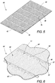
- Fig. 5 depicts a substantially optically transparent top sheet 60 that includes a substrate 62 and a conductive collection grid, generally indicated at 64, applied to the substrate.
- substrate 62 may be constructed from a clear polymer
- grid 64 may be constructed from a suitable conductive metal such as copper or silver which is printed, etched, electroplated or otherwise applied to the substrate.
- Grid 64 generally includes collection lines or "fingers" 66, buss bars 68, and interconnection tabs 70 extending from each buss bar.
- Fig. 6 is a magnified view depicting a portion of an alternative substantially optically transparent top sheet 60'.
- sheet 60' of Fig. 6 also includes a substrate 62' and a conductive collection grid, generally indicated at 64', applied to the substrate.
- grid 64' of top sheet 60' includes collection lines or "fingers" 66', buss bars 68', and interconnection tabs 70' extending from each buss bar.
- lines 66', buss bars 68' and interconnection tabs 70' are slightly different in top sheet 60' than their counterparts in top sheet 60.
- grid lines 66' form a plurality of closed rectangular loops rather than just individual linear extensions from the buss bar
- buss bar 68' includes mechanical stress relieving serpentine portions 69'
- interconnection tabs 70' include interconnection fiducial lines 71' (depicted as circular in Fig. 6).
- Fig. 6 also shows semi-transparent dielectric strips 72' attached to the top sheet and covering buss bars 68'. These strips could be applied in a similar manner to top sheet 60. The function of fiducial lines 71' and dielectric strips 72' will be described below.
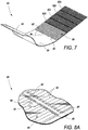
- FIGs. 7 and Figs. 8A-8B depict yet another intermediate article of manufacture, generally indicated at 80, according to aspects of the present teachings. More specifically, Fig. 7 shows a perspective view of intermediate article 80, Fig. 8A shows a magnified perspective view of a portion of the intermediate article, and Fig. 8B shows an exploded view of the portion of the intermediate article shown in Fig. 8A .
- Intermediate article 80 includes a plurality of photovoltaic cells 82a, 82b, 82c, 82d, each of which may be substantially similar to cell 50 described previously (see Fig. 4 ).
- Cells 82 have been positioned on a substantially optically transparent top sheet, generally indicated at 84, which is similar to top sheets 60 and 60' (see Figs. 5-6 ).
- the views of Figs. 7 and Figs. 8A-8B all depict article 80 from the side opposite the side where the cells contact the top sheet, i.e., the views of Figs. 7-8 are looking through the transparent top sheet.
- Top sheet 84 includes a clear polymer layer 86, upon which has been printed a conductive grid pattern, generally indicated at 88.
- grid pattern 88 includes buss bars 90 and grid lines 92 extending from each buss bar.
- Grid lines 92 form a plurality of closed paths, rather than simply forming individual lines extending from the buss bars. This provides some redundancy in the grid pattern, in case the conductive path along a particular grid line becomes interrupted, for instance if the grid line happens to be damaged.
- a plurality of interconnection tabs 94 also extend from each buss bar, from a side opposite the side from which the grid lines extend.
- Buss bars 90, grid lines 92 and tabs 94 all form a continuous electrically conductive grid pattern 88.
- dielectric strips 96 may be applied to cover the buss bars. This can help to prevent shunting in the regions where the cell edges are close to the buss bars.
- Figs. 8A-8B also depict how adjacent cells 82a and 82b may be electrically interconnected in series.
- cell 82b is positioned with its interconnection regions, generally indicated at 98, each overlapping at least one of the interconnection tabs 94 of grid pattern 88.
- each cell will overlap a plurality of interconnection tabs of the grid pattern.
- regions 98 are electrically isolated from the remainder of the photoactive top surface of cell 82b.
- any portion of cell 82b in electrical contact with the interconnection tab 94 shown in Figs. 8A-8B will also be in electrical contact with corresponding buss bar 90 and grid lines 92 of grid pattern 88, and thus with the top photoactive surface of adjacent cell 82a. As will be described in more detail below, this facilitates electrical series connection of the adjacent cells.
- reliable physical and electrical contact between the cells and the collection grid may be obtained as a result of an eventual lamination step, which typically also involves one or more additional encapsulant layers disposed below the cells and/or above the top sheet.
- it may improve durability to add an adhesive layer between the cells and the grid.
- This adhesive layer (not shown) may be applied to the cells, the grid, or both.
- the use of an adhesive that is thermally curable has the advantage that it may be cured automatically during the module lamination process.
- a suitable adhesive will be substantially optically transparent, to maximize the amount of solar radiation reaching the photovoltaic cells.
- the adhesive also may be electrically conductive.
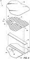
- Fig. 9 is a magnified perspective view similar to Fig. 8B , except that in Fig. 9 , a central portion of interconnection region 98 of cell 82b has been electrically connected to interconnection tab 94 of grid pattern 88, as indicated by circular regions 110 of the cell interconnection region and the grid interconnection tab.
- the central portions of interconnection regions 98 of cell 82b may be laser welded to central portions of corresponding interconnection tabs 94. Laser welding generally causes the interconnection tabs to make electrical contact with the conductive substrate of cell 82b, for example by melting, vaporizing, obliterating or otherwise penetrating the photoactive layers above the substrate of cell 82b.
- laser welding may convert the photoactive layers into material having low ohmic resistance (for example, resistance of 0.1 milliohms-cm 2 or less), thus allowing an electrical connection between the conductive grid pattern and the underlying conductive substrate of cell 82b.
- the laser welding operation may cause the metal of the interconnection tabs and/or the substrate to melt together to some extent, so that the tabs and the substrate become joined together as the molten metal comingles and cools.
- grid pattern 88 which is in electrical contact with the photoactive composition of cell 82b, is placed into electrical contact with portions of the substrate of cell 82b located within the interconnection areas of cell 82b. This provides electrical interconnection of the top or "sunny" side of cell 82a with the opposite polarity side of cell 82b, i.e. cells 82a and 82b are electrically interconnected in series. Similarly, each pair of adjacent cells 82 in Fig. 7 may be electrically interconnected in series.
- various types of lasers may be used to laser weld photovoltaic cells to interconnection tabs of a connection grid, and the most appropriate laser may depend on the precise composition and thickness of the photoactive cell layers, the cell substrate, and/or the conductive grid.
- one type of laser that may be suitable is a continuous-wave fiber laser emitting at a wavelength of approximately 1070 nm and with a power of approximately 30-70 Watts, focused to a beam diameter of approximately 30-80 ⁇ m, scanned at a rate of approximately 400-800 mm/sec and in a circle of approximately 1-4 mm in diameter to produce a similar size weld.
- the laser will typically be directed to impinge first on the back side of the cell substrate, although in some cases the laser may be directed from the opposite side of the photovoltaic assembly, i.e. to impinge first on the transparent top sheet rather than the substrate.
- FIG. 10 depicts portions of a photovoltaic module, generally indicated at 200, in which a pair of adjacent photovoltaic cells 202a, 202b have been electrically interconnected in series.
- the interconnection of cells 202a and 202b is generally similar to the interconnection of cells 82a and 82b described above, except that the interconnection regions of the cells in module 200 are removed before the cells are interconnected, rather than as part of the interconnection process, as described below.
- each of cells 202a and 202b includes a conductive substrate which is overlaid with a photoactive composition, such as adjacent layers of n-type and p-type semiconductor material.
- a photoactive composition such as adjacent layers of n-type and p-type semiconductor material.
- other layers of material such as a back contact layer and/or a back side protective layer, also may be deposited on one or both sides of the substrate.
- a back side protective layer need not be electrically conductive, because electrical contact to the back side polarity is made through the front of the cell substrate.
- a low cost, stable coating such as an oxide or a nitride, may be used to protect the back side of the cell substrate.
- Photoactive material has been scribed away from portions of each cell, electrically isolating edge portions of the cells, including an interconnection area 208 of cell 202a, and exposing the conductive substrate. More generally, several such interconnection areas would exist on each cell.
- Cells 202a and 202b are disposed on an interconnection component, generally indicated at 210, which includes an optically transmissive top sheet 212 with a conductive grid pattern, generally indicated at 214, disposed on the side of the top sheet facing the cells, and a dielectric strip 216 covering a portion of the grid pattern including a buss bar 218, to prevent possible shorting (or "shunting") when cells 202a and 202b are positioned near each other on the interconnection component.
- an interconnection component generally indicated at 210, which includes an optically transmissive top sheet 212 with a conductive grid pattern, generally indicated at 214, disposed on the side of the top sheet facing the cells, and a dielectric strip 216 covering a portion of the grid pattern including a buss bar 218, to prevent possible shorting (or "shunting") when cells 202a and 202b are positioned near each other on the interconnection component.
- Grid pattern 214 electrically interconnects the adjacent cells by providing electrical contact between an interconnection tab 220 of the grid pattern and the conductive substrate of cell 202b in each interconnection area 208, and also directly contacting the photoactive composition of cell 202a.
- the conductive substrate of cell 202b in the interconnection area is electrically isolated from the top or "sunny" side of cell 202b, and therefore shares the polarity of the bottom side of the photoactive composition of cell 202b.
- Grid pattern 214 electrically connects this polarity of cell 202b with the top or "sunny" side polarity of cell 202a, forming an electrical series connection between the two adjacent cells.
- each interconnection area 208 may be formed from the conductive substrate side, whereas in other cases the photovoltaic assembly may be laser welded from the top sheet side. In either case, laser welding generally serves to form a strong bond between the metals of the substrate and the interconnection tabs, by melting comingling the metals, which then solidify to form a reliable physical and electrical connection.
- cells may be interconnected according to the present teachings by creating electrically isolated interconnection areas on each cell, where each electrically isolated interconnection area is characterized by an absence of photoactive composition within at least a portion of the interconnection area.
- the electrically isolated interconnection areas each may be characterized by an absence of photovoltaic composition around a perimeter of the interconnection area, prior to interconnecting the adjacent cells.
- the photovoltaic composition may be removed from the perimeter area, for example, by laser scribing, in some cases during the same scribing operation that removes the photoactive material from edge portions of each cell.
- cell interconnection may be accomplished by laser welding or otherwise modifying, penetrating, melting and/or obliterating some of the photoactive composition in a central portion of the electrically isolated interconnection areas, to form an electrical connection between the substrate of the corresponding cell and an overlying connection grid, which in turn makes electrical contact with the top or "sunny" side of the adjacent cell.
- the interconnection operation itself (e.g., laser welding) causes some additional removal of photovoltaic material from the interconnection areas.
- the photoactive composition may be removed from the interconnection areas prior to placement of the cells against the connection grid, for example by laser scribing the photoactive material off of the interconnection areas during the same scribing operation that removes the photoactive material from edge portions of each cell to help prevent shunting between cells.
- the electrically isolated interconnection areas each may be characterized by an absence of photoactive composition within substantially the entire interconnection area.
- An additional interconnection operation such as laser welding still may be used to form a reliable physical and electrical connection between the substrate and the interconnection tabs of the connection grid in the interconnection areas.
- Fig. 11 is a flow chart depicting a method, generally indicated at 300, of manufacturing a photovoltaic module according to aspects of the present teachings.
- suitable photovoltaic material including a photoactive composition deposited on a conductive substrate, has already been manufactured and is available to incorporate into a module.
- method 300 could include preliminary steps of manufacturing the photovoltaic material, as described, for example, in the references that have been incorporated into this disclosure.
- the photovoltaic material used in method 300 will generally be referred to as a photovoltaic "web.”
- the web of photovoltaic material is laser scribed to remove the photoactive composition and expose the conductive substrate in certain regions.
- the web may be scribed to define perimeter portions of individual cells and also to define perimeter portions of interconnect regions.
- the photoactive composition may be completely scribed away from the interconnect regions.
- the scribing performed in step 302 serves to electrically isolate the interconnection regions, provides reference lines for subsequent cutting operations, and isolates individual cells for voltage testing.
- the cell regions defined by the scribe lines are voltage tested. This is typically done in a roll-to-roll process, by irradiating the cells and simultaneously testing the voltage induced between the top and bottom of each cell or selected cells. This is a form of quality control that allows cells to be categorized by efficiency, or in extreme cases discarded.
- the web of photovoltaic material is slit into a plurality of reels, as depicted, for example, in Fig. 3 . This allows the web to be cut into desired widths for different products or applications, as the cell width is determined by the reel width.
- the reels of photovoltaic material are cut into individual cells, as depicted, for example, in Fig. 4 . This allows the reels to be cut into cells of any desired size, based on the fiducial lines that were scribed in step 302. Step 308 may be performed in a "step and repeat" motion so that the cells are cut at instants when the photovoltaic material is motionless or nearly so.
- a frontsheet (which also may be referred to as a top sheet) is prepared.
- Preparing the frontsheet will generally include applying a conductive grid pattern to one side of a substantially optically transparent planar material, such as a clear polymer material.
- the frontsheet may be constructed from a thermoplastic layer.
- a suitable thermoplastic layer may include an ionomer obtained from DuPont under the trade name Surlyn.
- the frontsheet is a clear sheet of starting substrate, for example (PET), which in this specific example has a thickness of approximately 50-microns.
- the PET receives an even extrusion coating of the ionomer everywhere on one side, for example, about 100-microns in thickness.
- the grid pattern is then applied to the frontsheet as described below.
- the grid pattern will generally include buss bars, grid lines, and interconnection pads configured to electrically interconnect adjacent photovoltaic cells placed in contact with the grid pattern, as described above.
- the grid pattern may be constructed from a conductive metal such as copper, and may be applied by any suitable method, such as printing.
- the grid pattern on the front sheet may be defined using an "etch resist" pattern, and then the copper in all other areas may be removed (chemically etched away). After the etch step, copper remains only in areas where it is desired to form the conductive grid and/or conducting traces for a reverse diode structure, to be described in more detail below.
- the frontsheet material remains exposed everywhere where the copper has been removed, i.e., around the grid structure.
- Preparing the frontsheet at step 310 also may include applying strips of dielectric material over the buss bars of the grid pattern to help prevent shunting where cell edges touch or come near the buss bars.
- the dielectric strips will typically be substantially transparent, and may be applied, for example, in a rotary printing process or any other suitable process.
- the dielectric may be cured, for instance in a fast ultraviolet curing process.
- the cells cut in step 306 are placed into suitable positions on the frontsheet prepared in step 308.
- This step may be performed as a "pick and place” operation, where the frontsheet moves forward by the length of one cell, stops as the cell is placed into position on the frontsheet, and then the movement is repeated.
- the cells will generally be placed into positions so that they may be electrically interconnected in series by the connection grid of the frontsheet, as described previously. Specifically, each cell will be placed with most of its surface contacting the grid lines of the frontsheet, and also with one or more electrically isolated interconnection areas of the cell overlapping interconnection pads of the frontsheet grid.
- each cell may be temporarily bonded in place, for example with a small amount of adhesive or by heat staking, as indicated at step 314.
- Heat staking may be accomplished by, for example, using direct heat from laser diodes, a laser, or hot air jets, which are directed at a small number of spots, for example, 1- to 2-cm in diameter, to melt an adjacent layer of the frontsheet and bond it to the cells.
- the partially assembled "prelaminate" structure also may passed through a pair of "nip" rollers to press the front sheet and the photovoltaic layers together, causing them to stick together in a few small spots, which is enough to hold the assembly together as it is rolled up.
- a thin layer of adhesive may be applied to the cells and/or the frontsheet before the cells are placed on the frontsheet.
- This adhesive will typically be curable in a subsequent lamination step, but may adhere sufficiently prior to lamination to hold the cells in place on the frontsheet during the manufacturing process. In a subsequent step later in the process, the entire assembly goes through final lamination where it is remelted, causing it to stick together everywhere.
- the portions of conductive substrate underlying the interconnection areas of each cell are physically and electrically connected to the interconnection pads of the frontsheet grid, typically by laser welding.
- laser welding a small central portion of each interconnection area has been found to cause modification, penetration or obliteration of the cell layers overlaying the cell substrate, so that the cell substrate is placed into electrical contact with the associated interconnection pad.
- laser welding causes robust physical attachment of the interconnection pads to the cell substrate.
- Laser welding may be performed either from the cell substrate side or from the frontsheet side of the assembly. The specifications of a suitable laser and laser welding operation have been described previously.
- a backsheet is prepared.
- the backsheet will be disposed beneath the conductive substrate of the cells, and can serve purposes such as insulating and/or protecting the back side of the photovoltaic assembly.
- the backsheet may include materials to resist corrosion, such as chromium, molybdenum, or suitable alloys thereof.
- the backsheet also may include one or more polymer layers, which may be constructed from materials such as PET, PEN, PEEK, polyimide, or ETFE, among others.
- back sheet includes a layer of thermoplastic material, such as an ionomer.
- the backsheet may include a layer of PET with a thickness of about 50-microns, with an extruded coating of ionomer applied across the surface at a thickness of about 100-microns.
- holes may be punched or otherwise formed in the backsheet to allow for testing and/or to provide access to the conductive back side of the assembly for electrical connections.
- the assembly is laminated to form a substantially complete module.
- Lamination may be performed in a single roll-to-roll operation after both the frontsheet and the backsheet are positioned on opposite sides of the photovoltaic cells, or alternatively, lamination may be performed in two or more separate operations.
- the frontsheet may be laminated to the cells before the backsheet is positioned, and then the backsheet may be laminated to the cells.
- additional lamination may be performed.
- additional components such as contact leads, a weatherproof front vapor barrier or cover glass, and a weatherproof back vapor barrier may be provided, and then a final lamination operation may be performed to complete the assembly.
- the module is cooled and light soaked, and then at step 324, the module is tested to measure cell performance. Finally, at step 326, the module may be cut or trimmed to remove any excess laminate from the edges, then binned according to performance and capacity, and packed for shipping.
- steps above can be performed in various orders, and in some cases steps may be omitted or replaced.
- testing may be performed after lamination of a backsheet to the back side of the cells, but before final lamination of weatherproof layers.
- the "prelaminate" formed by the lamination of a backsheet onto the cells may be cut to final module size before final lamination of weatherproof layers.
- Other variations are also possible. Accordingly, many methods are encompassed by the present teachings, and specifically by the method steps outlined above.
- each cell is forced to produce or conduct the same current as the entire string.
- a potential problem arises whenever one or several cells are 'shaded', reducing their produced current. For example, a cell might be literally shaded while others in the string remain exposed to sunlight, or a cell might stop performing at full capacity for some other reason.
- a string of any reasonable number of cells has a high enough voltage to exceed the reverse breakdown voltage of a single, shaded cell. In this case, the other cells force the string current through the shaded cells in a 'reverse' sense to the diode formed by the PV cell.
- photovoltaic modules incorporate bypass diodes to protect each cell, groups of cells, or the module from reverse currents and thus breakdown events with the attendant damage.
- Commercially produced silicon semiconductor or Schottky diodes are typically added to a photovoltaic module. In the most extensive cases, one or more diodes are added across each photovoltaic cell (in a reverse polarity).
- U.S. Patent No. 6,690,041 entitled “Monolithically Integrated Diodes in Thin Film Photovoltaic Devices,” describes a method of using a small area of the thin film photovoltaic material, adjacent to each cell, and interconnected using scribing and monolithic fabrication schemes, to form an integral bypass diode. This method avoids the expense of adding a discrete bypass diode, and retains the thin, continuous nature of the product, permitting a very lightweight, low cost, thin lamination package for the entire module.
- U.S. Patent No. 6,690,041 is disadvantageous in that it consumes frontside area, i.e., area that would otherwise be used to generate power.
- the area required for the bypass diode is governed by heat dissipation, and can be substantial.
- the former approach also requires that the bypass diode be of the same material as the photoactive material, and poses a somewhat cumbersome arrangement wherein the bypass diode for one cell is located on an adjacent cell.
- the concept described in the disclosure retains all the advantages of the concept of U.S. Patent No. 6,690,041 , but avoids the drawbacks mentioned above.
- Figs. 12-13 are isometric views schematically depicting intermediate stages in the manufacture of a photovoltaic assembly, generally indicated at 600, incorporating a bypass diode according to aspects of the present teachings.
- Assembly 600 includes a plurality of photovoltaic cells 602a, 602b, 602c, each of which is a thin film photovoltaic cell as described previously, such as a CIGS-based cell disposed on a stainless steel substrate.
- the cells of assembly 600 may be fixed in their relative positions through their attachment to a frontsheet (not shown in Figs. 12-13 ), as described previously.
- a dielectric material pattern 604 is printed or otherwise applied to the back side of cells 602 (i.e., in contact with the conductive substrate of the cells), spanning a pair of adjacent cells such as cells 602b, 602c. Although dielectric pattern 604 is shown attached only to cells 602b and 602c in Figs. 12-13 , the dielectric pattern would generally be repeated across each pair of adjacent cells.
- a thin film diode is then applied to the back side of dielectric pattern 604, spanning the same adjacent cells as the dielectric pattern.
- Thin film diode 606, the construction of which will be described in more detail below, includes an anode portion 608, partially overlaid by a cathode portion 610.
- Dielectric pattern 604 and thin film diode 606 are shaped so that the anode portion of the diode contacts the back side of one of the adjacent cells (cell 602c in Fig. 13 ), and the cathode portion of the diode contacts the back side of the other adjacent cell (cell 602b in Fig. 13 ).
- dielectric pattern 604 includes one or more cutouts 612 that expose anode portion 608 of the thin film diode to the conductive substrate of one cell, and one or more cutouts 614 that expose cathode portion 610 of the thin film diode to the conductive substrate of the adjacent cell. Because the front side of one cell is connected in electrical series with the back side of the adjacent cell (see Figs. 6-10 and accompanying description), the diode is effectively electrically connected to the front and back side of the same cell. The result is that diode 606 functions as a relatively light weight bypass diode, without reducing the exposed "sunny side" area of the photovoltaic assembly and without creating unwieldy lumps that might be difficult to laminate.
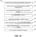
- Fig. 14 is a flow chart depicting a method, generally indicated at 650, of manufacturing a thin film bypass diode assembly and applying it to a photovoltaic cell, according to aspects of the present teachings.
- a thin film of p-type semiconductor material is deposited on a conductive substrate.
- the p-type semiconductor material of the thin film diode may be copper indium gallium selenide, or CIGS, deposited on a stainless steel or molybdenum substrate.
- the photoactive material of the thin film diode may be copper indium selenide, or CIS, also deposited on a stainless steel or molybdenum substrate. Using CIS reduces the semiconductor band gap and may improve the performance of the bypass diode.
- step 654 may include depositing additional layers of thin film materials to form a working diode.
- step 654 may include depositing cadmium selenide (CdS) and then a transparent conductive oxide (TCO), as in the manufacture of the primary photovoltaic cell material.
- the p-type semiconductor layer may be followed by aluminum, zinc or other metal metallization for an n-type Schottky contact to reduce the forward voltage drop and also to avoid the cost and complexity of the additional CdS and TCO layers.
- Steps 652 and 654 are typically performed in a reel-to-reel process, to produce a roll or "web" of thin film diode material that in many respects resembles a web of thin film photovoltaic material for photovoltaic cells. As described below, however, the thin film diode material will subsequently be processed in a manner specific to its use for bypass diodes.
- two-sided conductive tape is applied to the back side (substrate side) of the thin film diode material, and at step 658, the diode material is slit to width, for instance into relatively narrow reels of diode material.
- the diode material is attached to a conductive foil, typically constructed of copper, which has a greater width than the diode material.
- the conductive tape adheres the diode material to the copper foil, resulting in a strip of diode material on a copper foil that extends beyond the edges of the diode material on each lateral side.
- step 662 another layer of two-sided conductive tape is applied to the top side of the diode assembly, covering both the diode material and the copper foil.
- step 664 the diode assembly is singulated into individual bypass diodes, each of which may be applied to an individual photovoltaic cell at step 666, as described previously and shown in Fig. 12 .
- the conductive tape applied in both steps 656 and 662 can be "z-axis" conductive tape, meaning that it is only substantially electrically conductive in a direction perpendicular to the plane of the tape. This may help to avoid electrical shorts that might otherwise be caused by the tape.
- Figs. 15A-D show a thin film bypass diode assembly, generally indicated at 700, at various intermediate stages of manufacture.
- Bypass diode assembly 700 may result, for example, from method of manufacture 650 described above, and the intermediate stages of manufacture shown in Figs. 15A-D correspond to the steps of method 650 as described below.
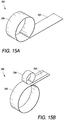
- Fig. 15A shows diode material 702, such as CIS-based semiconductor material on a stainless steel substrate, cut or slit into a relatively narrow reel, with conductive tape 704 being adhered to the back side (substrate side) of the material. This corresponds to the state of the diode assembly during step 658 of method 650.
- Fig. 15B shows diode material 702 and conductive tape 704 being adhered to a copper foil 706. This corresponds to the state of the diode assembly during step 660 of method 650.
- Fig. 15C shows another layer of conductive tape 707 being applied to the assembly of Fig. 15B , corresponding to the state of the diode assembly during step 662 of method 650.
- Fig. 15D shows the assembly of Fig. 15C after it has been cut or singulated into a thin film diode 708 with desired dimensions, corresponding to the state of the diode assembly after step 664 of method 650.
- a continuous ribbon of CIS-based or CIGS-based thin film diode material could be manufactured as described previously, but assembled into bypass diodes and/or attached to adjacent photovoltaic cells in an alternative manner.
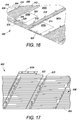
- Figs. 16-17 depict a photovoltaic module, generally indicated at 800, which incorporates an alternatively connected bypass diode.
- a pair of photovoltaic cells 802a, 802b are electrically interconnected by a frontsheet 804, which includes a conductive grid pattern, generally indicated at 806, applied to one side of a substantially optically transparent planar sheet 808, such as a clear polymer material.
- Grid pattern 806 includes buss bars 810, grid lines 812 and interconnection tabs or pads 814, all of which are substantially similar to their counterparts in previously described examples, such as in grid pattern 88 of Figs. 8A-8B and Fig. 9 .
- grid pattern 806 in Figs. 16-17 also includes buss bar extensions 815, each of which extends from one of the buss bars of the assembly. Buss bar extensions 815 are used to connect bypass diodes to the cells, as described below.
- Cells 802a and 802b are positioned so that they are electrically interconnected in series by the grid pattern, as described previously. Specifically, interconnection areas 816 of cell 802b may be laser welded to interconnection tabs 814 of the grid pattern, as indicated by weld circles 818, to electrically connect the back side of cell 802b to the front side of cell 802a.
- Assembly 800 also includes bypass diodes 820a, 820b, each of which is attached to a respective one of cells 802a, 802b.
- Each bypass diode includes a suitably modified thin-film semiconductor material 822 (as described previously) disposed upon a substrate 824 of stainless steel or some other suitable conductive material.
- the front or semiconductor side of diode 820b is placed into electrical contact with the back or substrate side of corresponding cell 802b, establishing the cathode of the diode. The diode extends beyond the edge of the cell to the associated buss bar extension 815.
- a portion of diode 820b overlapping the buss bar extension is electrically isolated from the portion of the diode overlapping cell 802b by a scribe line 826 across the width of the diode, which penetrates to the diode substrate.
- the portion of the diode overlapping the buss bar extension is then laser welded to the buss bar extension, which modifies, obliterates or otherwise penetrates the semiconductor material of the diode and forms an electrical connection between the substrate or back side of the diode and the buss bar extension, as indicated at weld circles 828. Because the buss bar extension is a portion of grid pattern 806, it is electrically connected to the front or "sunny" side of cell 802b.
- diode 820b is electrically connected to the front side of cell 802b, establishing the anode of the diode.
- Diode 820a would be electrically connected to cell 802a in precisely the same manner.
- the bypass diodes may be conveniently laminated to the backside of the cells at the "prelaminate" stage.
- the various structural members disclosed herein may be constructed from any suitable material, or combination of materials, such as metal, plastic, nylon, rubber, or any other materials with sufficient structural strength to withstand the loads incurred during use. Materials may be selected based on their durability, flexibility, weight, and/or aesthetic qualities.
Landscapes
- Photovoltaic Devices (AREA)
- Life Sciences & Earth Sciences (AREA)
- Engineering & Computer Science (AREA)
- Sustainable Energy (AREA)
- Sustainable Development (AREA)
Description
- The field of photovoltaics generally relates to multi-layer materials that convert sunlight directly into DC electrical power. The basic mechanism for this conversion is the photovoltaic effect, first observed by Antoine-César Becquerel in 1839, and first correctly described by Einstein in a seminal 1905 scientific paper for which he was awarded a Nobel Prize for physics. In the United States, photovoltaic (PV) devices are popularly known as solar cells or PV cells. Solar cells are typically configured as a cooperating sandwich of p-type and n-type semiconductors, in which the n-type semiconductor material (on one "side" of the sandwich) exhibits an excess of electrons, and the p-type semiconductor material (on the other "side" of the sandwich) exhibits an excess of holes, each of which signifies the absence of an electron. Near the p-n junction between the two materials, valence electrons from the n-type layer move into neighboring holes in the p-type layer, creating a small electrical imbalance inside the solar cell. This results in an electric field in the vicinity of the metallurgical junction that forms the electronic p-n junction.
- When an incident photon excites an electron in the cell into the conduction band, the excited electron becomes unbound from the atoms of the semiconductor, creating a free electron/hole pair. Because, as described above, the p-n junction creates an electric field in the vicinity of the junction, electron/hole pairs created in this manner near the junction tend to separate and move away from junction, with the electron moving toward the electrode on the n-type side, and the hole moving toward the electrode on the p-type side of the junction. This creates an overall charge imbalance in the cell, so that if an external conductive path is provided between the two sides of the cell, electrons will move from the n-type side back to the p-type side along the external path, creating an electric current. In practice, electrons may be collected from at or near the surface of the n-type side by a conducting grid that covers a portion of the surface, while still allowing sufficient access into the cell by incident photons.
- Such a photovoltaic structure, when appropriately located electrical contacts are included and the cell (or a series of cells) is incorporated into a closed electrical circuit, forms a working PV device. As a standalone device, a single conventional solar cell is not sufficient to power most applications. As a result, solar cells are commonly arranged into PV modules, or "strings," by connecting the front of one cell to the back of another, thereby adding the voltages of the individual cells together in electrical series. Typically, a significant number of cells are connected in series to achieve a usable voltage. The resulting DC current then may be fed through an inverter, where it is transformed into AC current at an appropriate frequency, which is chosen to match the frequency of AC current supplied by a conventional power grid. In the United States, this frequency is 60 Hertz (Hz), and most other countries provide AC power at either 50 Hz or 60 Hz.
- One particular type of solar cell that has been developed for commercial use is a "thin-film" PV cell. In comparison to other types of PV cells, such as crystalline silicon PV cells, thin-film PV cells require less light-absorbing semiconductor material to create a working cell, and thus can reduce processing costs. Thin-film based PV cells also offer reduced cost by employing previously developed deposition techniques for the electrode layers, where similar materials are widely used in the thin-film industries for protective, decorative, and functional coatings. Common examples of low cost commercial thin-film products include water impermeable coatings on polymer-based food packaging, decorative coatings on architectural glass, low emissivity thermal control coatings on residential and commercial glass, and scratch and anti-reflective coatings on eyewear. Adopting or modifying techniques that have been developed in these other fields has allowed a reduction in development costs for PV cell thin-film deposition techniques.
- Furthermore, thin-film cells have exhibited efficiencies approaching 20%, which rivals or exceeds the efficiencies of the most efficient crystalline cells. In particular, the semiconductor material copper indium gallium diselenide (CIGS) is stable, has low toxicity, and is truly a thin film, requiring a thickness of less than two microns in a working PV cell. As a result, to date CIGS appears to have demonstrated the greatest potential for high performance, low cost thin-film PV products, and thus for penetrating bulk power generation markets. Other semiconductor variants for thin-film PV technology include copper indium diselenide, copper indium disulfide, copper indium aluminum diselenide, and cadmium telluride.
- Some thin-film PV materials may be deposited either on rigid glass substrates, or on flexible substrates. Glass substrates are relatively inexpensive, generally have a coefficient of thermal expansion that is a relatively close match with the CIGS or other absorber layers, and allow for the use of vacuum deposition systems. However, when comparing technology options applicable during the deposition process, rigid substrates suffer from various shortcomings during processing, such as a need for substantial floor space for processing equipment and material storage, expensive and specialized equipment for heating glass uniformly to elevated temperatures at or near the glass annealing temperature, a high potential for substrate fracture with resultant yield loss, and higher heat capacity with resultant higher electricity cost for heating the glass. Furthermore, rigid substrates require increased shipping costs due to the weight and fragile nature of the glass. As a result, the use of glass substrates for the deposition of thin films may not be the best choice for low-cost, large-volume, high-yield, commercial manufacturing of multi-layer functional thin-film materials such as photovoltaics.
- In contrast, roll-to-roll processing of thin flexible substrates allows for the use of compact, less expensive vacuum systems, and of non-specialized equipment that already has been developed for other thin film industries. PV cells based on thin flexible substrate materials also exhibit a relatively high tolerance to rapid heating and cooling and to large thermal gradients (resulting in a low likelihood of fracture or failure during processing), require comparatively low shipping costs, and exhibit a greater ease of installation than cells based on rigid substrates. Additional details relating to the composition and manufacture of thin film PV cells of a type suitable for use with the presently disclosed methods and apparatus may be found, for example, in
U.S. Patent Nos. 6,310,281 ,6,372,538 , and7,194,197, all to Wendt et al. , andU.S. Patent No. 8,062,922 to Britt et al. - As noted previously, a significant number of PV cells often are connected in series to achieve a usable voltage, and thus a desired power output. Such a configuration is often called a "string" of PV cells. Due to the different properties of crystalline substrates and flexible thin film substrates, the electrical series connection between cells may be constructed differently for a thin film cell than for a crystalline cell, and forming reliable series connections between thin film cells poses several challenges. For example, soldering (the traditional technique used to connect crystalline solar cells) directly on thin film cells exposes the PV coatings of the cells to damaging temperatures, and the organic-based silver inks typically used to form a collection grid on thin film cells may not allow strong adherence by ordinary solder materials in any case. Thus, PV cells often are joined with wires or conductive tabs attached to the cells with an electrically conductive adhesive (ECA), rather than by soldering.
- However, even when wires or tabs are used to form inter-cell connections, the extremely thin coatings and potential flaking along cut PV cell edges introduces opportunities for shorting (power loss) wherever a wire or tab crosses over a cell edge. Furthermore, the conductive substrate on which the PV coatings are deposited, which typically is a metal foil, may be easily deformed by thermomechanical stress from attached wires and tabs. This stress can be transferred to weakly-adhering interfaces, which can result in delamination of the cells. In addition, adhesion between the ECA and the cell back side, or between the ECA and the conductive grid on the front side, can be weak, and mechanical stress may cause separation of the wires or tabs at these locations. Also, corrosion can occur between the molybdenum or other coating on the back side of a cell and the ECA that joins the tab to the solar cell there. This corrosion may result in a high-resistance contact or adhesion failure, leading to power losses.
- Advanced methods of joining thin film PV cells with conductive tabs or ribbons may largely overcome the problems of electrical shorting and delamination, but may require undesirably high production costs to do so. Furthermore, all such methods-no matter how robust-require that at least some portion of the PV string be covered by a conductive tab, which blocks solar radiation from striking that portion of the string and thus reduces the efficiency of the system. As a result, there is a need for improved methods of interconnecting PV cells into strings, and for improved strings of interconnected cells. Specifically, there is a need for strings and methods of their formation that reduce interconnection costs and reduce the fraction of each PV cell that is covered by the interconnection mechanism, while maintaining or improving the ability of the cell to withstand stress.
- The subject matter of the present invention is defined in
claims 1 and 9. - Photovoltaic module configurations include multiple flexible thin film photovoltaic cells electrically connected in series, and laminated to a substantially transparent top sheet having a conductive grid pattern facing the cells. A portion of the photoactive composition of each cell may be removed to expose the underlying conductive substrate, allowing cells to be interconnected by electrically connecting the conductive grid pattern contacting the top surface of one cell with the top side of the conductive substrate of an adjacent cell.
- Methods of manufacturing photovoltaic modules including integrated multi-cell interconnections are also described. Methods include steps of electrically isolating certain portions of cells to facilitate interconnection of the cells, by obliterating, removing or otherwise modifying photoactive material in cells to expose the underlying conductive substrate in certain regions, or to render the photoactive material sufficiently electrically conductive to form electrical connections with the conductive substrate. For example, methods according to the present teachings may include applying a conductive grid pattern to an optically transparent top sheet, aligning cells with the top sheet, and laser welding or otherwise securing the cells to the top sheet in the proper configuration. Laser welding may convert existing semiconductor material into material having low ohmic resistance (for example, resistance of 0.1 milliohms-cm2 or less), thus allowing an electrical connection between the conductive grid pattern and the conductive substrate of the cell to which it is welded.
- Numerous other devices, intermediate articles and methods of manufacture will be apparent from the detailed description below and related figures.
-
-
Fig. 1 is a perspective view of photovoltaic cell according to aspects of the present teachings. -
Fig. 2 is a perspective view of a roll of photovoltaic material with portions of a photoactive layer of the material scribed away, according to aspects of the present teachings. -
Fig. 3 is a perspective view of the photovoltaic material ofFig. 2 showing the material cut into several reels, according to aspects of the present teachings. -
Fig. 4 is a perspective view of a discrete photovoltaic cell that has been cut from one of the reels depicted inFig. 3 , according to aspects of the present teachings. -
Fig. 5 is a perspective view of an optically transparent top sheet with a conductive grid applied to the sheet, according to aspects of the present teachings. -
Fig. 6 is a magnified perspective view of another optically transparent top sheet with a conductive grid and strips of dielectric applied to the sheet, according to aspects of the present teachings. -
Fig. 7 is a perspective view of several discrete photovoltaic cells positioned on an optically transparent top sheet and on a conductive grid of the top sheet, according to aspects of the present teachings. -
Fig. 8A is a magnified view of portions of the cells, top sheet and grid ofFig. 7 , showing details of an interconnection region between the cells. -
Fig. 8B is an exploded view of the assembly ofFig. 8A . -
Fig. 9 is a magnified exploded view similar to the view ofFig. 8B , depicting a variation of the conductive grid according to aspects of the present teachings. -
Fig. 10 is top plan view of portions of two adjacent, photovoltaic cells positioned on a top sheet and a conductive grid, according to aspects of the present teachings. -
Fig. 11 is a flow diagram depicting a method of manufacturing a photovoltaic module, according to aspects of the present teachings. -
Fig. 12 is a schematic isometric view showing a dielectric material applied to the back side of two adjacent photovoltaic cells, according to aspects of the present teachings. -
Fig. 13 is a schematic isometric view showing a bypass diode assembly being applied to the adjacent cells ofFig. 12 . -
Fig. 14 is a flow chart depicting a method of manufacturing bypass diodes and applying them to photovoltaic cells, according to aspects of the present teachings. -
Fig. 15A is an isometric view depicting a first intermediate article of manufacture in the assembly of a bypass diode, according to aspects of the present teachings. -
Fig. 15B is an isometric view depicting a second intermediate article of manufacture in the assembly of a bypass diode, according to aspects of the present teachings. -
Fig. 15C is an isometric view depicting a third intermediate article of manufacture in the assembly of a bypass diode, according to aspects of the present teachings. -
Fig. 15D is an isometric view depicting a substantially completely assembled bypass diode, according to aspects of the present teachings. -
Fig. 16 is an isometric, partially exploded view showing bypass diodes being assembled to interconnected photovoltaic cells, according to aspects of the present teachings. -
Fig. 17 is an isometric, partially exploded view of the assembly ofFig. 16 , shown from the opposite side of the assembly. - Methods and apparatus for interconnecting flexible, thin-film photovoltaic (PV) cells in a scalable, efficient process, are provided. More specifically, examples of the present teachings relate to a roll-to-roll assembly of flexible PV cells on a flexible current-carrying back sheet. The back sheet may be a conductive substrate on which photoactive materials have been deposited.
- According to the present teachings, systems and methods of interconnecting thin-film photovoltaic cells in a flexible substrate package may include a series of photovoltaic cells and a transparent top sheet covering the cells. Electrically-conductive pathways are established connecting a top or "sunny" side of one cell to the top of the conductive substrate underlying the photoactive material of an adjacent cell. Portions of the photoactive material of the interconnected cells may be scribed away or otherwise removed, to expose the underlying conductive substrate and to facilitate interconnection. A conductive grid may be applied to the top sheet and configured to form electrical connections between adjacent cells that are placed in contact with the grid.
-
Figure 1 depicts a photovoltaic cell, generally indicated at 10, according to aspects of the present teachings.Cell 10 includes a plurality of discrete, interconnectedphotovoltaic portions cell 10 may be interconnected to form a module according to the present teachings. Each of the photovoltaic cells typically includes a conductive substrate, upon which are disposed various layers, including photoactive material such as adjacent layers of cadmium sulfide (CdS) and a layer of copper indium gallium diselenide (CIGS) to form a p-n junction. More details regarding the composition and manufacture of exemplary photovoltaic cells that may be used in conjunction with the present teachings are disclosed inU.S. Patent No. 8, 062,922 . -
Cell 10 also includes an optically transparenttop surface 20 overlying the photoactive surface. Aconductive grid 22 is configured to collect unbound electrons from a top surface of the cell. Buss bars 24 also may be applied to the top of the cell and interconnected with the conductive grid, to improve the collection of electrons by the grid.Cell 10 will generally be cut from a larger quantity of thin film, flexible photovoltaic material. -
Fig. 2 depicts an intermediate article of manufacture in the form of aroll 30 of photovoltaic material. The material ofroll 30 includes a conductive substrate and various layers overlying the substrate, and can be thought of as a continuous roll of material that may be cut into discrete cells such ascell 10 depicted inFig. 1 . The material ofroll 30 includesvarious portions 32 from which the layers overlying the conductive substrate have been obliterated, scribed away or otherwise removed, to expose the underlying substrate. For example, the overlying layers of material may be removed fromportions 32 of the material through laser scribing.Portions 32 where the substrate is exposed serve various purposes that will be described below. -
Fig. 3 depicts another intermediate article of manufacture in the form of a plurality ofreels 40 of photovoltaic material.Reels 40 have been formed by cutting or slittingroll 30, as should be apparent through comparison ofFig. 3 withFig. 2 .Fig. 4 depicts yet another intermediate article of manufacture in the form of a discretephotovoltaic cell 50, which has been formed by cutting the material of one ofreels 40 across its width.Cell 50 may be used in a module of interconnected photovoltaic cells, as described in more detail below. -
Fig. 4 also depicts inmore detail portions 32 from which the material overlying the conductive substrate has been removed. Specifically,portions 32 include both aperipheral outline portion 52 that lies just within the outer perimeter ofcell 50, and severalinterior outline portions 54.Peripheral outline portion 52 helps to electrically isolatecell 50 from adjacent cells and also helps to avoid unwanted shorting that may otherwise occur near the edges of the cell.Interior outline portions 54 define electrically isolated interconnection areas on the front side of each cell, which facilitate the interconnection of adjacent cells as described below. -
Fig. 5 depicts a substantially optically transparenttop sheet 60 that includes asubstrate 62 and a conductive collection grid, generally indicated at 64, applied to the substrate. For example,substrate 62 may be constructed from a clear polymer, andgrid 64 may be constructed from a suitable conductive metal such as copper or silver which is printed, etched, electroplated or otherwise applied to the substrate.Grid 64 generally includes collection lines or "fingers" 66, buss bars 68, andinterconnection tabs 70 extending from each buss bar. -
Fig. 6 is a magnified view depicting a portion of an alternative substantially optically transparent top sheet 60'. Liketop sheet 60 ofFig. 5 , sheet 60' ofFig. 6 also includes a substrate 62' and a conductive collection grid, generally indicated at 64', applied to the substrate. Also similarly totop sheet 60, grid 64' of top sheet 60' includes collection lines or "fingers" 66', buss bars 68', and interconnection tabs 70' extending from each buss bar. However, as depicted inFig. 6 , lines 66', buss bars 68' and interconnection tabs 70' are slightly different in top sheet 60' than their counterparts intop sheet 60. - More specifically, grid lines 66' form a plurality of closed rectangular loops rather than just individual linear extensions from the buss bar, buss bar 68' includes mechanical stress relieving serpentine portions 69', and interconnection tabs 70' include interconnection fiducial lines 71' (depicted as circular in
Fig. 6). Fig. 6 also shows semi-transparent dielectric strips 72' attached to the top sheet and covering buss bars 68'. These strips could be applied in a similar manner totop sheet 60. The function of fiducial lines 71' and dielectric strips 72' will be described below. -
Figs. 7 andFigs. 8A-8B depict yet another intermediate article of manufacture, generally indicated at 80, according to aspects of the present teachings. More specifically,Fig. 7 shows a perspective view ofintermediate article 80,Fig. 8A shows a magnified perspective view of a portion of the intermediate article, andFig. 8B shows an exploded view of the portion of the intermediate article shown inFig. 8A . -
Intermediate article 80 includes a plurality ofphotovoltaic cells cell 50 described previously (seeFig. 4 ). Cells 82 have been positioned on a substantially optically transparent top sheet, generally indicated at 84, which is similar totop sheets 60 and 60' (seeFigs. 5-6 ). The views ofFigs. 7 andFigs. 8A-8B all depictarticle 80 from the side opposite the side where the cells contact the top sheet, i.e., the views ofFigs. 7-8 are looking through the transparent top sheet. -
Top sheet 84 includes aclear polymer layer 86, upon which has been printed a conductive grid pattern, generally indicated at 88. As can be seen most clearly inFigs. 8A-8B ,grid pattern 88 includes buss bars 90 andgrid lines 92 extending from each buss bar.Grid lines 92 form a plurality of closed paths, rather than simply forming individual lines extending from the buss bars. This provides some redundancy in the grid pattern, in case the conductive path along a particular grid line becomes interrupted, for instance if the grid line happens to be damaged. - A plurality of
interconnection tabs 94 also extend from each buss bar, from a side opposite the side from which the grid lines extend. Buss bars 90,grid lines 92 andtabs 94 all form a continuous electricallyconductive grid pattern 88. Aftergrid pattern 88 is applied topolymer layer 86, dielectric strips 96 may be applied to cover the buss bars. This can help to prevent shunting in the regions where the cell edges are close to the buss bars. -
Figs. 8A-8B also depict howadjacent cells cell 82b is positioned with its interconnection regions, generally indicated at 98, each overlapping at least one of theinterconnection tabs 94 ofgrid pattern 88. Typically, as should be apparent fromFig. 7 , each cell will overlap a plurality of interconnection tabs of the grid pattern. Due to scribedperimeter 100 of the interconnection regions,regions 98 are electrically isolated from the remainder of the photoactive top surface ofcell 82b. However, any portion ofcell 82b in electrical contact with theinterconnection tab 94 shown inFigs. 8A-8B will also be in electrical contact withcorresponding buss bar 90 andgrid lines 92 ofgrid pattern 88, and thus with the top photoactive surface ofadjacent cell 82a. As will be described in more detail below, this facilitates electrical series connection of the adjacent cells. - In some cases, reliable physical and electrical contact between the cells and the collection grid may be obtained as a result of an eventual lamination step, which typically also involves one or more additional encapsulant layers disposed below the cells and/or above the top sheet. In other cases, however, it may improve durability to add an adhesive layer between the cells and the grid. This adhesive layer (not shown) may be applied to the cells, the grid, or both. The use of an adhesive that is thermally curable has the advantage that it may be cured automatically during the module lamination process. Generally, a suitable adhesive will be substantially optically transparent, to maximize the amount of solar radiation reaching the photovoltaic cells. The adhesive also may be electrically conductive.
-
Fig. 9 is a magnified perspective view similar toFig. 8B , except that inFig. 9 , a central portion ofinterconnection region 98 ofcell 82b has been electrically connected tointerconnection tab 94 ofgrid pattern 88, as indicated bycircular regions 110 of the cell interconnection region and the grid interconnection tab. For example, the central portions ofinterconnection regions 98 ofcell 82b may be laser welded to central portions ofcorresponding interconnection tabs 94. Laser welding generally causes the interconnection tabs to make electrical contact with the conductive substrate ofcell 82b, for example by melting, vaporizing, obliterating or otherwise penetrating the photoactive layers above the substrate ofcell 82b. Alternatively, laser welding may convert the photoactive layers into material having low ohmic resistance (for example, resistance of 0.1 milliohms-cm2 or less), thus allowing an electrical connection between the conductive grid pattern and the underlying conductive substrate ofcell 82b. - Furthermore, the laser welding operation may cause the metal of the interconnection tabs and/or the substrate to melt together to some extent, so that the tabs and the substrate become joined together as the molten metal comingles and cools. In any case, as a result of laser welding,
grid pattern 88, which is in electrical contact with the photoactive composition ofcell 82b, is placed into electrical contact with portions of the substrate ofcell 82b located within the interconnection areas ofcell 82b. This provides electrical interconnection of the top or "sunny" side ofcell 82a with the opposite polarity side ofcell 82b, i.e.cells Fig. 7 may be electrically interconnected in series. - According to the present teachings, various types of lasers may be used to laser weld photovoltaic cells to interconnection tabs of a connection grid, and the most appropriate laser may depend on the precise composition and thickness of the photoactive cell layers, the cell substrate, and/or the conductive grid. For example, to laser weld a 30 µm thick stainless steel cell substrate to a 37 µm thick copper interconnection grid tab, one type of laser that may be suitable is a continuous-wave fiber laser emitting at a wavelength of approximately 1070 nm and with a power of approximately 30-70 Watts, focused to a beam diameter of approximately 30-80 µm, scanned at a rate of approximately 400-800 mm/sec and in a circle of approximately 1-4 mm in diameter to produce a similar size weld. The laser will typically be directed to impinge first on the back side of the cell substrate, although in some cases the laser may be directed from the opposite side of the photovoltaic assembly, i.e. to impinge first on the transparent top sheet rather than the substrate.
- The general process of electrically connecting the top or "sunny" side of one cell to the top of the conductive substrate (and thus the opposite polarity) of an adjacent cell may be accomplished in various alternative ways. For example,
Fig. 10 depicts portions of a photovoltaic module, generally indicated at 200, in which a pair of adjacentphotovoltaic cells cells cells module 200 are removed before the cells are interconnected, rather than as part of the interconnection process, as described below. - Specifically, each of
cells interconnection area 208 ofcell 202a, and exposing the conductive substrate. More generally, several such interconnection areas would exist on each cell. -
Cells top sheet 212 with a conductive grid pattern, generally indicated at 214, disposed on the side of the top sheet facing the cells, and adielectric strip 216 covering a portion of the grid pattern including abuss bar 218, to prevent possible shorting (or "shunting") whencells - In
Fig. 10 , the perspective is from abovetop sheet 212, with the grid pattern and the cells both disposed on the far side of the top sheet.Grid pattern 214 electrically interconnects the adjacent cells by providing electrical contact between aninterconnection tab 220 of the grid pattern and the conductive substrate ofcell 202b in eachinterconnection area 208, and also directly contacting the photoactive composition ofcell 202a. The conductive substrate ofcell 202b in the interconnection area is electrically isolated from the top or "sunny" side ofcell 202b, and therefore shares the polarity of the bottom side of the photoactive composition ofcell 202b.Grid pattern 214 electrically connects this polarity ofcell 202b with the top or "sunny" side polarity ofcell 202a, forming an electrical series connection between the two adjacent cells. - Although
cells Fig. 10 , an additional interconnection step will still typically be used to form a more reliable electrical connection. For example, laser welding may be used to bond a central portion of eachinterconnection area 208 to thecorresponding interconnection tab 220. As described previously, in some cases the photovoltaic assembly may be laser welded from the conductive substrate side, whereas in other cases the photovoltaic assembly may be laser welded from the top sheet side. In either case, laser welding generally serves to form a strong bond between the metals of the substrate and the interconnection tabs, by melting comingling the metals, which then solidify to form a reliable physical and electrical connection. - More generally, cells may be interconnected according to the present teachings by creating electrically isolated interconnection areas on each cell, where each electrically isolated interconnection area is characterized by an absence of photoactive composition within at least a portion of the interconnection area. As depicted in
Figs. 7-9 and described above, the electrically isolated interconnection areas each may be characterized by an absence of photovoltaic composition around a perimeter of the interconnection area, prior to interconnecting the adjacent cells. The photovoltaic composition may be removed from the perimeter area, for example, by laser scribing, in some cases during the same scribing operation that removes the photoactive material from edge portions of each cell. - After the interconnection areas have been electrically isolated, cell interconnection may be accomplished by laser welding or otherwise modifying, penetrating, melting and/or obliterating some of the photoactive composition in a central portion of the electrically isolated interconnection areas, to form an electrical connection between the substrate of the corresponding cell and an overlying connection grid, which in turn makes electrical contact with the top or "sunny" side of the adjacent cell. In this case, the interconnection operation itself (e.g., laser welding) causes some additional removal of photovoltaic material from the interconnection areas.
- Alternatively, as depicted in
Fig. 10 and also described above, the photoactive composition may be removed from the interconnection areas prior to placement of the cells against the connection grid, for example by laser scribing the photoactive material off of the interconnection areas during the same scribing operation that removes the photoactive material from edge portions of each cell to help prevent shunting between cells. In this case, the electrically isolated interconnection areas each may be characterized by an absence of photoactive composition within substantially the entire interconnection area. An additional interconnection operation such as laser welding still may be used to form a reliable physical and electrical connection between the substrate and the interconnection tabs of the connection grid in the interconnection areas. -
Fig. 11 is a flow chart depicting a method, generally indicated at 300, of manufacturing a photovoltaic module according to aspects of the present teachings. Inmethod 300, it is assumed that suitable photovoltaic material, including a photoactive composition deposited on a conductive substrate, has already been manufactured and is available to incorporate into a module. In some cases, however,method 300 could include preliminary steps of manufacturing the photovoltaic material, as described, for example, in the references that have been incorporated into this disclosure. The photovoltaic material used inmethod 300 will generally be referred to as a photovoltaic "web." - At
step 302, the web of photovoltaic material is laser scribed to remove the photoactive composition and expose the conductive substrate in certain regions. Specifically, as depicted, for example, inFig. 2 , the web may be scribed to define perimeter portions of individual cells and also to define perimeter portions of interconnect regions. In some cases, as described previously (seeFig. 10 ), the photoactive composition may be completely scribed away from the interconnect regions. The scribing performed instep 302 serves to electrically isolate the interconnection regions, provides reference lines for subsequent cutting operations, and isolates individual cells for voltage testing. - At
step 304, the cell regions defined by the scribe lines are voltage tested. This is typically done in a roll-to-roll process, by irradiating the cells and simultaneously testing the voltage induced between the top and bottom of each cell or selected cells. This is a form of quality control that allows cells to be categorized by efficiency, or in extreme cases discarded. - At
step 306, the web of photovoltaic material is slit into a plurality of reels, as depicted, for example, inFig. 3 . This allows the web to be cut into desired widths for different products or applications, as the cell width is determined by the reel width. Atstep 308, the reels of photovoltaic material are cut into individual cells, as depicted, for example, inFig. 4 . This allows the reels to be cut into cells of any desired size, based on the fiducial lines that were scribed instep 302. Step 308 may be performed in a "step and repeat" motion so that the cells are cut at instants when the photovoltaic material is motionless or nearly so. - At
step 310, a frontsheet (which also may be referred to as a top sheet) is prepared. Preparing the frontsheet will generally include applying a conductive grid pattern to one side of a substantially optically transparent planar material, such as a clear polymer material. The frontsheet may be constructed from a thermoplastic layer. For instance, in one specific example, a suitable thermoplastic layer may include an ionomer obtained from DuPont under the trade name Surlyn. The frontsheet is a clear sheet of starting substrate, for example (PET), which in this specific example has a thickness of approximately 50-microns. The PET receives an even extrusion coating of the ionomer everywhere on one side, for example, about 100-microns in thickness. The grid pattern is then applied to the frontsheet as described below. - The grid pattern will generally include buss bars, grid lines, and interconnection pads configured to electrically interconnect adjacent photovoltaic cells placed in contact with the grid pattern, as described above. For example, any of the grid patterns depicted in
Figs. 5-10 may be suitable. The grid pattern may be constructed from a conductive metal such as copper, and may be applied by any suitable method, such as printing. Alternatively, the grid pattern on the front sheet may be defined using an "etch resist" pattern, and then the copper in all other areas may be removed (chemically etched away). After the etch step, copper remains only in areas where it is desired to form the conductive grid and/or conducting traces for a reverse diode structure, to be described in more detail below. The frontsheet material remains exposed everywhere where the copper has been removed, i.e., around the grid structure. - Preparing the frontsheet at
step 310 also may include applying strips of dielectric material over the buss bars of the grid pattern to help prevent shunting where cell edges touch or come near the buss bars. The dielectric strips will typically be substantially transparent, and may be applied, for example, in a rotary printing process or any other suitable process. Also as part of preparing the frontsheet, the dielectric may be cured, for instance in a fast ultraviolet curing process. - At
step 312, the cells cut instep 306 are placed into suitable positions on the frontsheet prepared instep 308. This step may be performed as a "pick and place" operation, where the frontsheet moves forward by the length of one cell, stops as the cell is placed into position on the frontsheet, and then the movement is repeated. The cells will generally be placed into positions so that they may be electrically interconnected in series by the connection grid of the frontsheet, as described previously. Specifically, each cell will be placed with most of its surface contacting the grid lines of the frontsheet, and also with one or more electrically isolated interconnection areas of the cell overlapping interconnection pads of the frontsheet grid. - After or during
placement step 312, each cell may be temporarily bonded in place, for example with a small amount of adhesive or by heat staking, as indicated atstep 314. Heat staking may be accomplished by, for example, using direct heat from laser diodes, a laser, or hot air jets, which are directed at a small number of spots, for example, 1- to 2-cm in diameter, to melt an adjacent layer of the frontsheet and bond it to the cells. The partially assembled "prelaminate" structure also may passed through a pair of "nip" rollers to press the front sheet and the photovoltaic layers together, causing them to stick together in a few small spots, which is enough to hold the assembly together as it is rolled up. - In some cases, alternatively or in addition to heat staking, a thin layer of adhesive may be applied to the cells and/or the frontsheet before the cells are placed on the frontsheet. This adhesive will typically be curable in a subsequent lamination step, but may adhere sufficiently prior to lamination to hold the cells in place on the frontsheet during the manufacturing process. In a subsequent step later in the process, the entire assembly goes through final lamination where it is remelted, causing it to stick together everywhere.
- At
step 316, the portions of conductive substrate underlying the interconnection areas of each cell are physically and electrically connected to the interconnection pads of the frontsheet grid, typically by laser welding. As described above, laser welding a small central portion of each interconnection area has been found to cause modification, penetration or obliteration of the cell layers overlaying the cell substrate, so that the cell substrate is placed into electrical contact with the associated interconnection pad. Furthermore, laser welding causes robust physical attachment of the interconnection pads to the cell substrate. Laser welding may be performed either from the cell substrate side or from the frontsheet side of the assembly. The specifications of a suitable laser and laser welding operation have been described previously. - At
step 318, a backsheet is prepared. The backsheet will be disposed beneath the conductive substrate of the cells, and can serve purposes such as insulating and/or protecting the back side of the photovoltaic assembly. For example, the backsheet may include materials to resist corrosion, such as chromium, molybdenum, or suitable alloys thereof. The backsheet also may include one or more polymer layers, which may be constructed from materials such as PET, PEN, PEEK, polyimide, or ETFE, among others. In a preferred embodiment, back sheet includes a layer of thermoplastic material, such as an ionomer. In a specific example, the backsheet may include a layer of PET with a thickness of about 50-microns, with an extruded coating of ionomer applied across the surface at a thickness of about 100-microns. As part ofstep 318, holes may be punched or otherwise formed in the backsheet to allow for testing and/or to provide access to the conductive back side of the assembly for electrical connections. - At
step 320, the assembly is laminated to form a substantially complete module. Lamination may be performed in a single roll-to-roll operation after both the frontsheet and the backsheet are positioned on opposite sides of the photovoltaic cells, or alternatively, lamination may be performed in two or more separate operations. For example, the frontsheet may be laminated to the cells before the backsheet is positioned, and then the backsheet may be laminated to the cells. Furthermore, even after both the frontsheet and the backsheet are laminated to the cells, additional lamination may be performed. For example, additional components such as contact leads, a weatherproof front vapor barrier or cover glass, and a weatherproof back vapor barrier may be provided, and then a final lamination operation may be performed to complete the assembly. - At
step 322, the module is cooled and light soaked, and then atstep 324, the module is tested to measure cell performance. Finally, atstep 326, the module may be cut or trimmed to remove any excess laminate from the edges, then binned according to performance and capacity, and packed for shipping. - The steps above can be performed in various orders, and in some cases steps may be omitted or replaced. For example, testing may be performed after lamination of a backsheet to the back side of the cells, but before final lamination of weatherproof layers. Similarly, the "prelaminate" formed by the lamination of a backsheet onto the cells may be cut to final module size before final lamination of weatherproof layers. Other variations are also possible. Accordingly, many methods are encompassed by the present teachings, and specifically by the method steps outlined above.
- The next portion of the present disclosure describes the use of thin film bypass diodes in conjunction with the previously described photovoltaic assemblies and method of manufacture; see
Figs. 12-17 . - To produce useful voltages, individual photovoltaic cells are serially connected in photovoltaic modules. Since the current must be the same at all points in a series circuit, each cell is forced to produce or conduct the same current as the entire string. A potential problem arises whenever one or several cells are 'shaded', reducing their produced current. For example, a cell might be literally shaded while others in the string remain exposed to sunlight, or a cell might stop performing at full capacity for some other reason. A string of any reasonable number of cells has a high enough voltage to exceed the reverse breakdown voltage of a single, shaded cell. In this case, the other cells force the string current through the shaded cells in a 'reverse' sense to the diode formed by the PV cell.
- This usually causes irreversible damage to the shaded cell (a permanent shunt at the site of the reverse breakdown), and subsequently a permanent loss in power output even when the shade is removed. Moreover, a 'hot spot' can appear at the site of reverse breakdown in the shaded cell, causing damage to the PV package, or even a safety hazard due to the danger of fire.
- The potential for cell damage due to current forced through the cell is a feature of all photovoltaic systems, including crystalline silicon and thin film types. Typically, photovoltaic modules incorporate bypass diodes to protect each cell, groups of cells, or the module from reverse currents and thus breakdown events with the attendant damage. Commercially produced silicon semiconductor or Schottky diodes, usually in a standard electronics package with tab or axial leads, are typically added to a photovoltaic module. In the most extensive cases, one or more diodes are added across each photovoltaic cell (in a reverse polarity).
- Drawbacks of the standard approach are significantly increased cost, added manufacturing complexity, multiple fragile connections, and added failure points. Another disadvantage is that these discrete bypass diode devices create hot spots in and of themselves, by virtue of the significant heat dissipation in a small volume during the bypass operation. Excessive temperatures may cause the bypass diode to fail, or damage the photovoltaic module package.
- For thin film flexible photovoltaic products, which are intended to be lightweight, several more serious drawbacks accrue because the discrete bypass diodes are of substantial thickness (often 2-5 mm). As a result, encapsulating these parts inside the protective package of the photovoltaic module necessarily increases the package thickness substantially (and thus the cost and weight, with reduced flexibility). The complexity and speed of lamination processes are adversely affected by the inclusion of the discrete diodes in the laminated package, making periodic "lumps" that must be processed without causing damage.
-
U.S. Patent No. 6,690,041 entitled "Monolithically Integrated Diodes in Thin Film Photovoltaic Devices," describes a method of using a small area of the thin film photovoltaic material, adjacent to each cell, and interconnected using scribing and monolithic fabrication schemes, to form an integral bypass diode. This method avoids the expense of adding a discrete bypass diode, and retains the thin, continuous nature of the product, permitting a very lightweight, low cost, thin lamination package for the entire module. - However, the approach of
U.S. Patent No. 6,690,041 is disadvantageous in that it consumes frontside area, i.e., area that would otherwise be used to generate power. The area required for the bypass diode is governed by heat dissipation, and can be substantial. The former approach also requires that the bypass diode be of the same material as the photoactive material, and poses a somewhat cumbersome arrangement wherein the bypass diode for one cell is located on an adjacent cell. The concept described in the disclosure retains all the advantages of the concept ofU.S. Patent No. 6,690,041 , but avoids the drawbacks mentioned above. -
Figs. 12-13 are isometric views schematically depicting intermediate stages in the manufacture of a photovoltaic assembly, generally indicated at 600, incorporating a bypass diode according to aspects of the present teachings.Assembly 600 includes a plurality ofphotovoltaic cells assembly 600 may be fixed in their relative positions through their attachment to a frontsheet (not shown inFigs. 12-13 ), as described previously. - A
dielectric material pattern 604 is printed or otherwise applied to the back side of cells 602 (i.e., in contact with the conductive substrate of the cells), spanning a pair of adjacent cells such ascells dielectric pattern 604 is shown attached only tocells Figs. 12-13 , the dielectric pattern would generally be repeated across each pair of adjacent cells. - As can be seen in
Fig. 13 , a thin film diode, generally indicated at 606, is then applied to the back side ofdielectric pattern 604, spanning the same adjacent cells as the dielectric pattern.Thin film diode 606, the construction of which will be described in more detail below, includes ananode portion 608, partially overlaid by acathode portion 610.Dielectric pattern 604 andthin film diode 606 are shaped so that the anode portion of the diode contacts the back side of one of the adjacent cells (cell 602c inFig. 13 ), and the cathode portion of the diode contacts the back side of the other adjacent cell (cell 602b inFig. 13 ). - More specifically,
dielectric pattern 604 includes one ormore cutouts 612 that exposeanode portion 608 of the thin film diode to the conductive substrate of one cell, and one ormore cutouts 614 that exposecathode portion 610 of the thin film diode to the conductive substrate of the adjacent cell. Because the front side of one cell is connected in electrical series with the back side of the adjacent cell (seeFigs. 6-10 and accompanying description), the diode is effectively electrically connected to the front and back side of the same cell. The result is thatdiode 606 functions as a relatively light weight bypass diode, without reducing the exposed "sunny side" area of the photovoltaic assembly and without creating unwieldy lumps that might be difficult to laminate. -
Fig. 14 is a flow chart depicting a method, generally indicated at 650, of manufacturing a thin film bypass diode assembly and applying it to a photovoltaic cell, according to aspects of the present teachings. Atstep 652, a thin film of p-type semiconductor material is deposited on a conductive substrate. For example, the p-type semiconductor material of the thin film diode may be copper indium gallium selenide, or CIGS, deposited on a stainless steel or molybdenum substrate. Alternatively, the photoactive material of the thin film diode may be copper indium selenide, or CIS, also deposited on a stainless steel or molybdenum substrate. Using CIS reduces the semiconductor band gap and may improve the performance of the bypass diode. - This may be followed at
step 654 by depositing additional layers of thin film materials to form a working diode. For example, step 654 may include depositing cadmium selenide (CdS) and then a transparent conductive oxide (TCO), as in the manufacture of the primary photovoltaic cell material. Alternatively, the p-type semiconductor layer may be followed by aluminum, zinc or other metal metallization for an n-type Schottky contact to reduce the forward voltage drop and also to avoid the cost and complexity of the additional CdS and TCO layers. -
Steps - At
step 656, two-sided conductive tape is applied to the back side (substrate side) of the thin film diode material, and atstep 658, the diode material is slit to width, for instance into relatively narrow reels of diode material. Atstep 660, the diode material is attached to a conductive foil, typically constructed of copper, which has a greater width than the diode material. The conductive tape adheres the diode material to the copper foil, resulting in a strip of diode material on a copper foil that extends beyond the edges of the diode material on each lateral side. - At
step 662, another layer of two-sided conductive tape is applied to the top side of the diode assembly, covering both the diode material and the copper foil. Atstep 664, the diode assembly is singulated into individual bypass diodes, each of which may be applied to an individual photovoltaic cell atstep 666, as described previously and shown inFig. 12 . The conductive tape applied in bothsteps -
Figs. 15A-D show a thin film bypass diode assembly, generally indicated at 700, at various intermediate stages of manufacture.Bypass diode assembly 700 may result, for example, from method ofmanufacture 650 described above, and the intermediate stages of manufacture shown inFigs. 15A-D correspond to the steps ofmethod 650 as described below. - Specifically,
Fig. 15A showsdiode material 702, such as CIS-based semiconductor material on a stainless steel substrate, cut or slit into a relatively narrow reel, withconductive tape 704 being adhered to the back side (substrate side) of the material. This corresponds to the state of the diode assembly duringstep 658 ofmethod 650.Fig. 15B showsdiode material 702 andconductive tape 704 being adhered to acopper foil 706. This corresponds to the state of the diode assembly duringstep 660 ofmethod 650.Fig. 15C shows another layer ofconductive tape 707 being applied to the assembly ofFig. 15B , corresponding to the state of the diode assembly duringstep 662 ofmethod 650.Fig. 15D shows the assembly ofFig. 15C after it has been cut or singulated into athin film diode 708 with desired dimensions, corresponding to the state of the diode assembly afterstep 664 ofmethod 650. - Alternative methods of constructing thin film bypass diodes, and incorporating them into photovoltaic modules, are also contemplated by the present teachings. For example, a continuous ribbon of CIS-based or CIGS-based thin film diode material could be manufactured as described previously, but assembled into bypass diodes and/or attached to adjacent photovoltaic cells in an alternative manner.
-
Figs. 16-17 depict a photovoltaic module, generally indicated at 800, which incorporates an alternatively connected bypass diode. In this example, a pair ofphotovoltaic cells frontsheet 804, which includes a conductive grid pattern, generally indicated at 806, applied to one side of a substantially optically transparentplanar sheet 808, such as a clear polymer material.Grid pattern 806 includes buss bars 810,grid lines 812 and interconnection tabs orpads 814, all of which are substantially similar to their counterparts in previously described examples, such as ingrid pattern 88 ofFigs. 8A-8B andFig. 9 . However,grid pattern 806 inFigs. 16-17 also includesbuss bar extensions 815, each of which extends from one of the buss bars of the assembly.Buss bar extensions 815 are used to connect bypass diodes to the cells, as described below. -
Cells interconnection areas 816 ofcell 802b may be laser welded tointerconnection tabs 814 of the grid pattern, as indicated byweld circles 818, to electrically connect the back side ofcell 802b to the front side ofcell 802a. -
Assembly 800 also includesbypass diodes cells substrate 824 of stainless steel or some other suitable conductive material. Considering the concrete example ofbypass diode 820b inFigs. 16-17 , the front or semiconductor side ofdiode 820b is placed into electrical contact with the back or substrate side ofcorresponding cell 802b, establishing the cathode of the diode. The diode extends beyond the edge of the cell to the associatedbuss bar extension 815. - A portion of
diode 820b overlapping the buss bar extension is electrically isolated from the portion of thediode overlapping cell 802b by ascribe line 826 across the width of the diode, which penetrates to the diode substrate. The portion of the diode overlapping the buss bar extension is then laser welded to the buss bar extension, which modifies, obliterates or otherwise penetrates the semiconductor material of the diode and forms an electrical connection between the substrate or back side of the diode and the buss bar extension, as indicated at weld circles 828. Because the buss bar extension is a portion ofgrid pattern 806, it is electrically connected to the front or "sunny" side ofcell 802b. Accordingly, the back side ofdiode 820b is electrically connected to the front side ofcell 802b, establishing the anode of the diode.Diode 820a would be electrically connected tocell 802a in precisely the same manner. According to the present teachings, the bypass diodes may be conveniently laminated to the backside of the cells at the "prelaminate" stage. - While the concepts discussed above have been described primarily in the context of flexible substrates having thin film CIGS photovoltaic layers, it should be understood that many of the concepts may also be readily used advantageously with other thin film devices and processes, for example, based on cadmium telluride, as well as rigid silicon based photovoltaic devices.
- The various structural members disclosed herein may be constructed from any suitable material, or combination of materials, such as metal, plastic, nylon, rubber, or any other materials with sufficient structural strength to withstand the loads incurred during use. Materials may be selected based on their durability, flexibility, weight, and/or aesthetic qualities.
Claims (13)
- A method of manufacturing a photovoltaic module, comprising:applying a photoactive composition to a conductive substrate to produce a continuous sheet of photovoltaic material;removing photoactive composition from the photovoltaic material to create a plurality of electrically isolated interconnection areas each electrically isolated from the photoactive composition disposed outside the interconnection areas;cutting the photovoltaic material into at least first and second discrete, physically separate photoactive cells wherein the first cell includes the interconnection areas;placing the cells in contact with an optically transmissive top sheet and thereby placing a conductive grid pattern of the top sheet into electrical contact with the interconnection areas of the first cell and the photoactive composition of the second cell; andelectrically interconnecting the cells by converting photoactive composition within the interconnection areas of the first cell into material having low ohmic resistance by laser welding, thus electrically connecting a portion of the grid pattern in electrical contact with the photoactive composition of the second cell to portions of the substrate located within the interconnection areas of the first cell.
- The method of claim 1, wherein removing photoactive composition from the first cell includes laser scribing a perimeter portion of each interconnection area.
- The method of claim 2, further comprising laser scribing a perimeter portion of each cell.
- The method of claim 1, wherein converting a portion of the photoactive composition within each interconnection area into material having low ohmic resistance includes laser welding the top sheet to a portion of each interconnection area.
- The method of claim 4, wherein laser welding includes directing a laser to impinge first on a back side of the substrate of the first cell.
- The method of claim 4, wherein laser welding includes directing a laser to impinge first on the top sheet.
- The method of claim 1, wherein the top sheet includes an adhesive layer disposed upon a structural layer.
- The method of claim 1, wherein the photoactive composition includes a p-type semiconductor layer formed of copper indium gallium diselenide (CIGS), and an n-type semiconductor layer formed of cadmium sulfide (CdS).
- A photovoltaic module, comprising:an optically transmissive top sheet including a conductive grid pattern disposed on one side of the top sheet; andfirst and second electrically interconnected discrete photovoltaic cells disposed on the top sheet with the conductive grid pattern in electrical contact with both of the cells, each cell including a photoactive composition applied to a conductive substrate and wherein the conductive substrate of the first cell is physically separate from the conductive substrate of the second cell;wherein the first cell includes a plurality of interconnection regions electrically isolated from the photovoltaic composition surrounding the interconnection regions, each interconnection region characterized by an absence of photovoltaic composition around a perimeter of the interconnection region and the presence of low ohmic resistance material within a central portion; andwherein the grid pattern electrically interconnects the cells by forming an electrical connection with the low ohmic resistance material and thus with the conductive substrate of the first cell in the interconnection regions, and forming an electrical connection with a top surface of the photoactive composition of the second cell.
- The module of claim 9, wherein the low ohmic resistance material is formed by laser welding the interconnection regions of the first cell to the top sheet.
- The module of claim 9, wherein the module is flexible and the photoactive composition includes a p-type semiconductor thin film layer formed of copper indium gallium diselenide (CIGS), and an n-type semiconductor thin film layer formed of cadmium sulfide (CdS).
- The module of claim 9, wherein the grid pattern includes a buss bar extending across the second cell and a plurality of interconnection tabs extending from the buss bar, each tab configured to make contact with one of the interconnection regions of the first cell.
- The module of claim 12, further comprising a strip of dielectric disposed between the buss bar and the second cell.
Applications Claiming Priority (2)
| Application Number | Priority Date | Filing Date | Title |
|---|---|---|---|
| US201261625553P | 2012-04-17 | 2012-04-17 | |
| PCT/US2013/037024 WO2013158796A1 (en) | 2012-04-17 | 2013-04-17 | Integrated thin film solar cell interconnection |
Publications (3)
| Publication Number | Publication Date |
|---|---|
| EP2839502A1 EP2839502A1 (en) | 2015-02-25 |
| EP2839502A4 EP2839502A4 (en) | 2015-12-02 |
| EP2839502B1 true EP2839502B1 (en) | 2017-01-04 |
Family
ID=49323976
Family Applications (1)
| Application Number | Title | Priority Date | Filing Date |
|---|---|---|---|
| EP13777853.6A Not-in-force EP2839502B1 (en) | 2012-04-17 | 2013-04-17 | Integrated thin film solar cell interconnection |
Country Status (5)
| Country | Link |
|---|---|
| US (2) | US9385254B2 (en) |
| EP (1) | EP2839502B1 (en) |
| CN (2) | CN107634108B (en) |
| HK (1) | HK1245504A1 (en) |
| WO (1) | WO2013158796A1 (en) |
Cited By (1)
| Publication number | Priority date | Publication date | Assignee | Title |
|---|---|---|---|---|
| TWI708402B (en) * | 2020-01-20 | 2020-10-21 | 友達光電股份有限公司 | Solar cell |
Families Citing this family (65)
| Publication number | Priority date | Publication date | Assignee | Title |
|---|---|---|---|---|
| US8759664B2 (en) | 2009-12-28 | 2014-06-24 | Hanergy Hi-Tech Power (Hk) Limited | Thin film solar cell strings |
| WO2013158796A1 (en) | 2012-04-17 | 2013-10-24 | Global Solar Energy, Inc. | Integrated thin film solar cell interconnection |
| USD750556S1 (en) * | 2014-11-19 | 2016-03-01 | Sunpower Corporation | Solar panel |
| USD933584S1 (en) | 2012-11-08 | 2021-10-19 | Sunpower Corporation | Solar panel |
| USD1009775S1 (en) | 2014-10-15 | 2024-01-02 | Maxeon Solar Pte. Ltd. | Solar panel |
| USD767484S1 (en) | 2014-11-19 | 2016-09-27 | Sunpower Corporation | Solar panel |
| WO2014117138A1 (en) | 2013-01-28 | 2014-07-31 | Global Solar Energy, Inc. | Photovoltaic interconnect systems, devices, and methods |
| USD914590S1 (en) * | 2013-04-26 | 2021-03-30 | Soliculture, Inc. | Solar module |
| US10940562B2 (en) | 2017-01-31 | 2021-03-09 | Nuburu, Inc. | Methods and systems for welding copper using blue laser |
| US10656328B2 (en) | 2016-04-29 | 2020-05-19 | Nuburu, Inc. | Monolithic visible wavelength fiber laser |
| US11612957B2 (en) * | 2016-04-29 | 2023-03-28 | Nuburu, Inc. | Methods and systems for welding copper and other metals using blue lasers |
| US10562132B2 (en) | 2013-04-29 | 2020-02-18 | Nuburu, Inc. | Applications, methods and systems for materials processing with visible raman laser |
| US10971896B2 (en) | 2013-04-29 | 2021-04-06 | Nuburu, Inc. | Applications, methods and systems for a laser deliver addressable array |
| US10940536B2 (en) | 2013-04-29 | 2021-03-09 | Nuburu, Inc. | Devices, systems and methods for three-dimensional printing |
| CN106165115A (en) * | 2013-11-14 | 2016-11-23 | 纽升股份有限公司 | Method during flexible solar battery is delivered to reel-to-reel module assembled |
| USD772800S1 (en) * | 2014-02-25 | 2016-11-29 | Derek Djeu | Solar cell backing plate |
| EP3149775B1 (en) * | 2014-05-27 | 2019-12-04 | SunPower Corporation | Shingled solar cell module |
| US11646549B2 (en) | 2014-08-27 | 2023-05-09 | Nuburu, Inc. | Multi kW class blue laser system |
| USD999723S1 (en) | 2014-10-15 | 2023-09-26 | Sunpower Corporation | Solar panel |
| USD913210S1 (en) | 2014-10-15 | 2021-03-16 | Sunpower Corporation | Solar panel |
| USD933585S1 (en) | 2014-10-15 | 2021-10-19 | Sunpower Corporation | Solar panel |
| USD896747S1 (en) | 2014-10-15 | 2020-09-22 | Sunpower Corporation | Solar panel |
| US10381493B2 (en) | 2014-10-31 | 2019-08-13 | Byd Company Limited | Solar cell unit, solar cell array, solar cell module and manufacturing method thereof |
| USD780108S1 (en) | 2015-06-23 | 2017-02-28 | Global Solar Energy, Inc. | Photovoltaic submodule |
| USD780109S1 (en) | 2015-06-23 | 2017-02-28 | Global Solar Energy, Inc. | Photovoltaic submodule |
| USD779426S1 (en) | 2015-06-23 | 2017-02-21 | Global Solar Energy, Inc. | Photovoltaic submodule |
| KR102206858B1 (en) * | 2015-09-22 | 2021-01-22 | 코오롱인더스트리 주식회사 | Flexible device, and method for manufacturing the same |
| US10040271B1 (en) | 2015-10-02 | 2018-08-07 | Global Solar Energy, Inc. | Metalization of flexible polymer sheets |
| US10131998B2 (en) | 2015-10-02 | 2018-11-20 | Global Solar Energy, Inc. | Metalization of flexible polymer sheets |
| US20220072659A1 (en) * | 2016-04-29 | 2022-03-10 | Nuburu, Inc. | Methods and Systems for Reducing Hazardous Byproduct from Welding Metals Using Lasers |
| US11980970B2 (en) | 2016-04-29 | 2024-05-14 | Nuburu, Inc. | Visible laser additive manufacturing |
| US12172377B2 (en) | 2016-04-29 | 2024-12-24 | Nuburu, Inc. | Blue laser metal additive manufacturing system |
| KR20210134087A (en) * | 2016-04-29 | 2021-11-08 | 누부루 인크. | Visible laser welding of electronic packaging, automotive electrics, battery and other components |
| USD877060S1 (en) * | 2016-05-20 | 2020-03-03 | Solaria Corporation | Solar module |
| US20170373211A1 (en) * | 2016-06-24 | 2017-12-28 | Merlin Solar Technologies, Inc. | Cell-to-cell interconnect |
| CN106449872B (en) * | 2016-09-28 | 2017-09-15 | 夏颖 | A kind of CIGS flexible battery piece cutting mechanisms automatically controlled |
| US10115855B2 (en) | 2016-09-30 | 2018-10-30 | Sunpower Corporation | Conductive foil based metallization of solar cells |
| US10461685B2 (en) * | 2016-10-04 | 2019-10-29 | Global Solar Energy, Inc. | Foldable photovoltaic assembly with non-perpendicular interconnection |
| CN108231936A (en) * | 2016-12-20 | 2018-06-29 | 北京汉能创昱科技有限公司 | A kind of solar cell module and preparation method thereof |
| CN108231935A (en) * | 2016-12-20 | 2018-06-29 | 北京汉能创昱科技有限公司 | Solar cell module and preparation method thereof |
| CN106898665B (en) * | 2017-02-09 | 2019-01-29 | 北京四方创能光电科技有限公司 | A kind of tandem flexible thin-film solar cell component and preparation method thereof |
| USD841570S1 (en) * | 2017-08-25 | 2019-02-26 | Flex Ltd | Solar cell |
| EP4220252A3 (en) | 2017-04-21 | 2023-08-09 | Nuburu, Inc. | Multi-clad optical fiber |
| WO2018231884A1 (en) | 2017-06-13 | 2018-12-20 | Nuburu, Inc. | Very dense wavelength beam combined laser system |
| USD855016S1 (en) * | 2017-10-24 | 2019-07-30 | Flex Ltd. | Solar cell |
| USD855017S1 (en) * | 2017-10-24 | 2019-07-30 | Flex Ltd. | Solar cell |
| TW201942418A (en) * | 2018-04-02 | 2019-11-01 | 美商全球太陽能公司 | Metalization of flexible polymer sheets |
| USD911263S1 (en) * | 2018-08-31 | 2021-02-23 | Rafael Badilla | Solar panel |
| CN110931582A (en) * | 2018-09-20 | 2020-03-27 | 北京铂阳顶荣光伏科技有限公司 | Solar cell front plate and method of making the same |
| WO2020107030A1 (en) | 2018-11-23 | 2020-05-28 | Nuburu, Inc | Multi-wavelength visible laser source |
| US11978815B2 (en) | 2018-12-27 | 2024-05-07 | Solarpaint Ltd. | Flexible photovoltaic cell, and methods and systems of producing it |
| US11081606B2 (en) * | 2018-12-27 | 2021-08-03 | Solarpaint Ltd. | Flexible and rollable photovoltaic cell having enhanced properties of mechanical impact absorption |
| US12628437B2 (en) | 2018-12-27 | 2026-05-12 | Solarpaint Ltd. | Injection molded, blow molded, and rotational molded articles that integrally incorporate a photovoltaic device, and method and system for producing such articles |
| EP3917718A4 (en) | 2019-02-02 | 2022-12-07 | Nuburu, Inc. | HIGH-BRIGHTNESS, HIGH-POWER, HIGH-RELIABILITY BLUE LASER DIODE SYSTEMS AND METHODS OF MAKING THEREOF |
| CN109877454B (en) * | 2019-04-11 | 2021-02-09 | 武汉华工激光工程有限责任公司 | Laser welding method for thin-film solar cell electrode |
| US20220270925A1 (en) * | 2019-07-22 | 2022-08-25 | Massachusetts Institute Of Technology | Flexing semiconductor structures and related techniques |
| CN111463321B (en) * | 2020-04-13 | 2021-09-24 | 上海绿兆新能源科技有限公司 | A welding head for reflective film photovoltaic modules |
| CN112071933B (en) * | 2020-08-31 | 2025-10-10 | 泰州隆基乐叶光伏科技有限公司 | Method and equipment for manufacturing interconnection component |
| CN112809176B (en) * | 2021-01-14 | 2023-04-11 | 北方夜视技术股份有限公司 | Nickel pipe manufacturing clamp and method for low-light-level image intensifier photocathode evaporation source |
| CN113020901B (en) * | 2021-02-02 | 2022-12-30 | 中交三航(南通)海洋工程有限公司 | Steel plate splicing construction process for large-diameter variable-diameter section steel pipe pile |
| WO2023154934A2 (en) * | 2022-02-13 | 2023-08-17 | Aptera Motors Corp. | Plant providing continuous process for making laminated solar panels |
| CN114975663B (en) * | 2022-04-29 | 2024-07-16 | 上海德瀛睿创半导体科技有限公司 | Solder strip, photovoltaic module, and preparation method and equipment of photovoltaic module |
| DE102022114036A1 (en) * | 2022-06-02 | 2023-12-07 | Glasfabrik Lamberts GmbH + Co. KG. | Multifunctional profiled glass sheet and profiled glass arrangement containing it |
| CN115939253A (en) * | 2022-11-21 | 2023-04-07 | 苏州迈展自动化科技有限公司 | A kind of photovoltaic solar cell module and preparation method thereof |
| JP7584072B1 (en) * | 2023-11-17 | 2024-11-15 | 株式会社Pxp | Solar Cell Module |
Family Cites Families (141)
| Publication number | Priority date | Publication date | Assignee | Title |
|---|---|---|---|---|
| FR1552078A (en) | 1967-11-15 | 1969-01-03 | ||
| JPS5628383B2 (en) | 1975-03-25 | 1981-07-01 | ||
| US4064552A (en) | 1976-02-03 | 1977-12-20 | Angelucci Thomas L | Multilayer flexible printed circuit tape |
| US4254546A (en) | 1978-09-11 | 1981-03-10 | Ses, Incorporated | Photovoltaic cell array |
| US4221465A (en) | 1978-09-28 | 1980-09-09 | Rca Corporation | Patching tape for diffractive subtractive filter viewgraphs |
| US4318938A (en) | 1979-05-29 | 1982-03-09 | The University Of Delaware | Method for the continuous manufacture of thin film solar cells |
| US4400577A (en) | 1981-07-16 | 1983-08-23 | Spear Reginald G | Thin solar cells |
| EP0078541B1 (en) | 1981-11-04 | 1991-01-16 | Kanegafuchi Kagaku Kogyo Kabushiki Kaisha | Flexible photovoltaic device |
| US4430519A (en) | 1982-05-28 | 1984-02-07 | Amp Incorporated | Electron beam welded photovoltaic cell interconnections |
| EP0112856A1 (en) | 1982-07-05 | 1984-07-11 | Hartag Ag | Installation consisting of panels, each of them comprising a plurality of photoelectric elements to produce a current |
| US4737379A (en) | 1982-09-24 | 1988-04-12 | Energy Conversion Devices, Inc. | Plasma deposited coatings, and low temperature plasma method of making same |
| AU2095083A (en) | 1982-11-09 | 1984-05-17 | Energy Conversion Devices Inc. | Laminated strip of large area solar cells |
| JPS604270A (en) | 1983-06-22 | 1985-01-10 | Hitachi Ltd | Manufacture of solar battery |
| JPS60123073A (en) | 1983-12-08 | 1985-07-01 | Fuji Electric Corp Res & Dev Ltd | Thin-film solar cell |
| US4542255A (en) | 1984-01-03 | 1985-09-17 | Atlantic Richfield Company | Gridded thin film solar cell |
| US4574160A (en) | 1984-09-28 | 1986-03-04 | The Standard Oil Company | Flexible, rollable photovoltaic cell module |
| US4697041A (en) | 1985-02-15 | 1987-09-29 | Teijin Limited | Integrated solar cells |
| US4617421A (en) | 1985-04-01 | 1986-10-14 | Sovonics Solar Systems | Photovoltaic cell having increased active area and method for producing same |
| US4783421A (en) | 1985-04-15 | 1988-11-08 | Solarex Corporation | Method for manufacturing electrical contacts for a thin-film semiconductor device |
| US4617420A (en) | 1985-06-28 | 1986-10-14 | The Standard Oil Company | Flexible, interconnected array of amorphous semiconductor photovoltaic cells |
| US4652693A (en) | 1985-08-30 | 1987-03-24 | The Standard Oil Company | Reformed front contact current collector grid and cell interconnect for a photovoltaic cell module |
| US4663828A (en) | 1985-10-11 | 1987-05-12 | Energy Conversion Devices, Inc. | Process and apparatus for continuous production of lightweight arrays of photovoltaic cells |
| US4642413A (en) | 1985-10-11 | 1987-02-10 | Energy Conversion Devices, Inc. | Power generating optical filter |
| US4713493A (en) | 1985-10-11 | 1987-12-15 | Energy Conversion Devices, Inc. | Power generating optical filter |
| US4663829A (en) | 1985-10-11 | 1987-05-12 | Energy Conversion Devices, Inc. | Process and apparatus for continuous production of lightweight arrays of photovoltaic cells |
| US4698455A (en) | 1986-11-04 | 1987-10-06 | Spectrolab, Inc. | Solar cell with improved electrical contacts |
| US4746618A (en) | 1987-08-31 | 1988-05-24 | Energy Conversion Devices, Inc. | Method of continuously forming an array of photovoltaic cells electrically connected in series |
| US4773944A (en) | 1987-09-08 | 1988-09-27 | Energy Conversion Devices, Inc. | Large area, low voltage, high current photovoltaic modules and method of fabricating same |
| US4965655A (en) | 1987-12-10 | 1990-10-23 | Minnesota Mining And Manufacturing Company | Interconnected semiconductor devices |
| US5021099A (en) | 1988-08-09 | 1991-06-04 | The Boeing Company | Solar cell interconnection and packaging using tape carrier |
| US4888061A (en) | 1988-09-01 | 1989-12-19 | Minnesota Mining And Manufacturing Company | Thin-film solar cells resistant to damage during flexion |
| US5118361A (en) | 1990-05-21 | 1992-06-02 | The Boeing Company | Terrestrial concentrator solar cell module |
| US5273608A (en) | 1990-11-29 | 1993-12-28 | United Solar Systems Corporation | Method of encapsulating a photovoltaic device |
| ES2134795T3 (en) * | 1991-02-21 | 1999-10-16 | Angew Solarenergie Ase Gmbh | PHOTOVOLTAIC DEVICE AND SOLAR MODULE FOR PARTIAL TRANSPARENCY; AND MANUFACTURING PROCEDURE. |
| US5258236A (en) | 1991-05-03 | 1993-11-02 | Ibm Corporation | Multi-layer thin film structure and parallel processing method for fabricating same |
| US5176758A (en) | 1991-05-20 | 1993-01-05 | United Solar Systems Corporation | Translucent photovoltaic sheet material and panels |
| US5181968A (en) | 1991-06-24 | 1993-01-26 | United Solar Systems Corporation | Photovoltaic device having an improved collector grid |
| US5185042A (en) | 1991-08-01 | 1993-02-09 | Trw Inc. | Generic solar cell array using a printed circuit substrate |
| US5391235A (en) | 1992-03-31 | 1995-02-21 | Canon Kabushiki Kaisha | Solar cell module and method of manufacturing the same |
| US5268037A (en) * | 1992-05-21 | 1993-12-07 | United Solar Systems Corporation | Monolithic, parallel connected photovoltaic array and method for its manufacture |
| JP2974513B2 (en) | 1992-09-03 | 1999-11-10 | キヤノン株式会社 | Roof material integrated solar cell module |
| US5385848A (en) | 1993-09-20 | 1995-01-31 | Iowa Thin Film Technologies, Inc | Method for fabricating an interconnected array of semiconductor devices |
| US5460659A (en) | 1993-12-10 | 1995-10-24 | Spectrolab, Inc. | Concentrating photovoltaic module and fabrication method |
| US5457057A (en) | 1994-06-28 | 1995-10-10 | United Solar Systems Corporation | Photovoltaic module fabrication process |
| US5474621A (en) | 1994-09-19 | 1995-12-12 | Energy Conversion Devices, Inc. | Current collection system for photovoltaic cells |
| JP2992464B2 (en) | 1994-11-04 | 1999-12-20 | キヤノン株式会社 | Covering wire for current collecting electrode, photovoltaic element using the covering wire for current collecting electrode, and method of manufacturing the same |
| US5928437A (en) | 1995-02-09 | 1999-07-27 | The Boeing Company | Microarray for efficient energy generation for satellites |
| US5547516A (en) | 1995-05-15 | 1996-08-20 | Luch; Daniel | Substrate structures for integrated series connected photovoltaic arrays and process of manufacture of such arrays |
| US6459032B1 (en) | 1995-05-15 | 2002-10-01 | Daniel Luch | Substrate structures for integrated series connected photovoltaic arrays and process of manufacture of such arrays |
| US5735966A (en) | 1995-05-15 | 1998-04-07 | Luch; Daniel | Substrate structures for integrated series connected photovoltaic arrays and process of manufacture of such arrays |
| US20080314433A1 (en) | 1995-05-15 | 2008-12-25 | Daniel Luch | Substrate structures for integrated series connected photovoltaic arrays and process of manufacture of such arrays |
| US7732243B2 (en) | 1995-05-15 | 2010-06-08 | Daniel Luch | Substrate structures for integrated series connected photovoltaic arrays and process of manufacture of such arrays |
| JP2992638B2 (en) | 1995-06-28 | 1999-12-20 | キヤノン株式会社 | Electrode structure and manufacturing method of photovoltaic element and solar cell |
| JP3222361B2 (en) | 1995-08-15 | 2001-10-29 | キヤノン株式会社 | Method of manufacturing solar cell module and solar cell module |
| DE19652810A1 (en) | 1996-12-18 | 1998-07-02 | Priesemuth W | Solar cell with p=n barrier type semiconductor layer |
| US6148570A (en) | 1998-02-05 | 2000-11-21 | Powerlight Corporation | Photovoltaic building assembly with continuous insulation layer |
| JPH1177348A (en) * | 1997-08-29 | 1999-03-23 | Canon Inc | Welding method and photovoltaic element |
| JPH11186572A (en) | 1997-12-22 | 1999-07-09 | Canon Inc | Photovoltaic element module |
| DE19814780A1 (en) | 1998-04-02 | 1999-07-22 | Ver Glaswerke Gmbh | Photovoltaic solar module |
| US6248948B1 (en) | 1998-05-15 | 2001-06-19 | Canon Kabushiki Kaisha | Solar cell module and method of producing the same |
| US8222513B2 (en) | 2006-04-13 | 2012-07-17 | Daniel Luch | Collector grid, electrode structures and interconnect structures for photovoltaic arrays and methods of manufacture |
| US7635810B2 (en) | 1999-03-30 | 2009-12-22 | Daniel Luch | Substrate and collector grid structures for integrated photovoltaic arrays and process of manufacture of such arrays |
| US20080011350A1 (en) | 1999-03-30 | 2008-01-17 | Daniel Luch | Collector grid, electrode structures and interconnect structures for photovoltaic arrays and other optoelectric devices |
| US20120171802A1 (en) | 2006-04-13 | 2012-07-05 | Daniel Luch | Collector grid and interconnect structures for photovoltaic arrays and modules |
| US20090293941A1 (en) | 2008-06-02 | 2009-12-03 | Daniel Luch | Photovoltaic power farm structure and installation |
| US20090111206A1 (en) | 1999-03-30 | 2009-04-30 | Daniel Luch | Collector grid, electrode structures and interrconnect structures for photovoltaic arrays and methods of manufacture |
| US8076568B2 (en) | 2006-04-13 | 2011-12-13 | Daniel Luch | Collector grid and interconnect structures for photovoltaic arrays and modules |
| US20090107538A1 (en) | 2007-10-29 | 2009-04-30 | Daniel Luch | Collector grid and interconnect structures for photovoltaic arrays and modules |
| US20100108118A1 (en) | 2008-06-02 | 2010-05-06 | Daniel Luch | Photovoltaic power farm structure and installation |
| US6239352B1 (en) | 1999-03-30 | 2001-05-29 | Daniel Luch | Substrate and collector grid structures for electrically interconnecting photovoltaic arrays and process of manufacture of such arrays |
| US8138413B2 (en) | 2006-04-13 | 2012-03-20 | Daniel Luch | Collector grid and interconnect structures for photovoltaic arrays and modules |
| US7507903B2 (en) | 1999-03-30 | 2009-03-24 | Daniel Luch | Substrate and collector grid structures for integrated series connected photovoltaic arrays and process of manufacture of such arrays |
| EP1194956A4 (en) | 1999-06-21 | 2005-01-19 | Aec Able Eng Co Inc | SOLAR BATTERY |
| JP4186756B2 (en) | 2003-08-29 | 2008-11-26 | 松下電器産業株式会社 | Circuit board and manufacturing method thereof |
| US20110067754A1 (en) | 2000-02-04 | 2011-03-24 | Daniel Luch | Substrate structures for integrated series connected photovoltaic arrays and process of manufacture of such arrays |
| US7898054B2 (en) | 2000-02-04 | 2011-03-01 | Daniel Luch | Substrate structures for integrated series connected photovoltaic arrays and process of manufacture of such arrays |
| US7898053B2 (en) | 2000-02-04 | 2011-03-01 | Daniel Luch | Substrate structures for integrated series connected photovoltaic arrays and process of manufacture of such arrays |
| US20130052769A1 (en) | 2000-02-04 | 2013-02-28 | Daniel Luch | Substrate structures for integrated series connected photovoltaic arrays and process of manufacture of such arrays |
| US8198696B2 (en) | 2000-02-04 | 2012-06-12 | Daniel Luch | Substrate structures for integrated series connected photovoltaic arrays and process of manufacture of such arrays |
| DE20002827U1 (en) | 2000-02-17 | 2000-05-04 | Röhm GmbH, 64293 Darmstadt | Photovoltaic element |
| US6372538B1 (en) | 2000-03-16 | 2002-04-16 | University Of Delaware | Fabrication of thin-film, flexible photovoltaic module |
| US6310281B1 (en) | 2000-03-16 | 2001-10-30 | Global Solar Energy, Inc. | Thin-film, flexible photovoltaic module |
| US7194197B1 (en) | 2000-03-16 | 2007-03-20 | Global Solar Energy, Inc. | Nozzle-based, vapor-phase, plume delivery structure for use in production of thin-film deposition layer |
| US6706963B2 (en) | 2002-01-25 | 2004-03-16 | Konarka Technologies, Inc. | Photovoltaic cell interconnection |
| US6653718B2 (en) | 2001-01-11 | 2003-11-25 | Honeywell International, Inc. | Dielectric films for narrow gap-fill applications |
| WO2003038859A2 (en) | 2001-07-20 | 2003-05-08 | Itn Energy Systems, Inc. | Apparatus and method of production of thin film photovoltaic modules |
| FR2831714B1 (en) | 2001-10-30 | 2004-06-18 | Dgtec | ASSEMBLY OF PHOTOVOLTAIC CELLS |
| US20030121228A1 (en) | 2001-12-31 | 2003-07-03 | Stoehr Robert P. | System and method for dendritic web solar cell shingling |
| US7365266B2 (en) | 2002-03-12 | 2008-04-29 | United Solar Ovonic Llc | Method and system for mounting photovoltaic material |
| US6690041B2 (en) * | 2002-05-14 | 2004-02-10 | Global Solar Energy, Inc. | Monolithically integrated diodes in thin-film photovoltaic devices |
| US7612283B2 (en) * | 2002-07-09 | 2009-11-03 | Canon Kabushiki Kaisha | Solar power generation apparatus and its manufacturing method |
| US6803513B2 (en) | 2002-08-20 | 2004-10-12 | United Solar Systems Corporation | Series connected photovoltaic module and method for its manufacture |
| DE10239845C1 (en) | 2002-08-29 | 2003-12-24 | Day4 Energy Inc | Electrode for photovoltaic cells, photovoltaic cell and photovoltaic module |
| US20100193367A1 (en) | 2004-02-11 | 2010-08-05 | Daniel Luch | Methods and structures for the production of electrically treated items and electrical connections |
| US20050176270A1 (en) | 2004-02-11 | 2005-08-11 | Daniel Luch | Methods and structures for the production of electrically treated items and electrical connections |
| US7122398B1 (en) | 2004-03-25 | 2006-10-17 | Nanosolar, Inc. | Manufacturing of optoelectronic devices |
| JP2006013403A (en) | 2004-06-29 | 2006-01-12 | Sanyo Electric Co Ltd | SOLAR CELL, SOLAR CELL MODULE, ITS MANUFACTURING METHOD, AND ITS REPAIR METHOD |
| US7838868B2 (en) | 2005-01-20 | 2010-11-23 | Nanosolar, Inc. | Optoelectronic architecture having compound conducting substrate |
| US7276724B2 (en) | 2005-01-20 | 2007-10-02 | Nanosolar, Inc. | Series interconnected optoelectronic device module assembly |
| US7517465B2 (en) | 2004-10-21 | 2009-04-14 | United Solar Ovonic Llc | Ultra lightweight photovoltaic device and method for its manufacture |
| US7176543B2 (en) | 2005-01-26 | 2007-02-13 | United Solar Ovonic Corp. | Method of eliminating curl for devices on thin flexible substrates, and devices made thereby |
| US7256140B2 (en) | 2005-09-20 | 2007-08-14 | United Solar Ovonic Llc | Higher selectivity, method for passivating short circuit current paths in semiconductor devices |
| US20070095384A1 (en) | 2005-10-28 | 2007-05-03 | Farquhar Donald S | Photovoltaic modules and interconnect methodology for fabricating the same |
| EP1941276A1 (en) | 2005-10-29 | 2008-07-09 | Bayer Technology Services GmbH | Process for determining one or more analytes in samples of biological origin having complex composition, and use thereof |
| US7498508B2 (en) | 2006-02-24 | 2009-03-03 | Day4 Energy, Inc. | High voltage solar cell and solar cell module |
| US9236512B2 (en) | 2006-04-13 | 2016-01-12 | Daniel Luch | Collector grid and interconnect structures for photovoltaic arrays and modules |
| US9006563B2 (en) | 2006-04-13 | 2015-04-14 | Solannex, Inc. | Collector grid and interconnect structures for photovoltaic arrays and modules |
| US8822810B2 (en) | 2006-04-13 | 2014-09-02 | Daniel Luch | Collector grid and interconnect structures for photovoltaic arrays and modules |
| US8729385B2 (en) | 2006-04-13 | 2014-05-20 | Daniel Luch | Collector grid and interconnect structures for photovoltaic arrays and modules |
| US8440907B2 (en) * | 2006-04-14 | 2013-05-14 | Sharp Kabushiki Kaisha | Solar cell, solar cell string and solar cell module |
| US20070283997A1 (en) | 2006-06-13 | 2007-12-13 | Miasole | Photovoltaic module with integrated current collection and interconnection |
| US20070283996A1 (en) | 2006-06-13 | 2007-12-13 | Miasole | Photovoltaic module with insulating interconnect carrier |
| JP5121181B2 (en) | 2006-07-28 | 2013-01-16 | 三洋電機株式会社 | Photovoltaic element and manufacturing method thereof |
| EP1898470B1 (en) | 2006-08-30 | 2011-07-27 | Keiwa Inc. | Use of a back sheet for photovoltaic modules and resulting photovoltaic module |
| US20080090022A1 (en) | 2006-10-12 | 2008-04-17 | Energy Conversion Devices, Inc. | High rate, continuous deposition of high quality amorphous, nanocrystalline, microcrystalline or polycrystalline materials |
| US7812247B2 (en) | 2006-10-23 | 2010-10-12 | Ascent Solar Technologies Inc. | Flexible photovoltaic array with integrated wiring and control circuitry, and associated methods |
| WO2008050626A1 (en) | 2006-10-23 | 2008-05-02 | Daikin Industries, Ltd. | Solar cell module, laminate, and method for production of solar cell module |
| JP4294048B2 (en) | 2006-11-29 | 2009-07-08 | 三洋電機株式会社 | Solar cell module |
| US7799182B2 (en) | 2006-12-01 | 2010-09-21 | Applied Materials, Inc. | Electroplating on roll-to-roll flexible solar cell substrates |
| CN103077978B (en) | 2007-02-16 | 2016-12-28 | 纳克公司 | The technique of solar battery structure, photovoltaic module and correspondence |
| WO2008116134A2 (en) * | 2007-03-22 | 2008-09-25 | United Solar Ovonic Llc | Method and apparatus for the laser scribing of ultra lightweight semiconductor devices |
| TWI335085B (en) | 2007-04-19 | 2010-12-21 | Ind Tech Res Inst | Bifacial thin film solar cell and method for fabricating the same |
| WO2009006230A2 (en) | 2007-06-30 | 2009-01-08 | Solannex, Inc. | Collector grid and interconnect structures for photovoltaic arrays and modules |
| US20090014058A1 (en) | 2007-07-13 | 2009-01-15 | Miasole | Rooftop photovoltaic systems |
| US8212139B2 (en) * | 2008-01-18 | 2012-07-03 | Tenksolar, Inc. | Thin-film photovoltaic module |
| DE212009000025U1 (en) | 2008-01-31 | 2010-09-23 | Global Solar Energy. Inc., Tuscon | Thin film solar cell sequence |
| EP2257970A4 (en) | 2008-03-05 | 2015-09-02 | Hanergy Hi Tech Power Hk Ltd | BUFFER LAYER DEPOSITION FOR THIN FILM SOLAR BATTERIES |
| US7968353B2 (en) | 2008-04-15 | 2011-06-28 | Global Solar Energy, Inc. | Apparatus and methods for manufacturing thin-film solar cells |
| US8207012B2 (en) | 2008-04-28 | 2012-06-26 | Solopower, Inc. | Method and apparatus for achieving low resistance contact to a metal based thin film solar cell |
| US20090272436A1 (en) | 2008-05-05 | 2009-11-05 | Osbert Hay Cheung | Non-glass photovoltaic module and methods for manufacture |
| US7638353B2 (en) | 2008-06-03 | 2009-12-29 | United Solar Ovonic Llc | Method for fabrication of semiconductor devices on lightweight substrates |
| US20090314330A1 (en) | 2008-06-24 | 2009-12-24 | Moser Baer Photovoltaic Limited | Photovoltaic module |
| EP2313926B1 (en) * | 2008-07-16 | 2019-06-12 | Merck Patent GmbH | Methods of preparing photovoltaic modules |
| US20100051085A1 (en) * | 2008-08-27 | 2010-03-04 | Weidman Timothy W | Back contact solar cell modules |
| NL2001958C (en) * | 2008-09-05 | 2010-03-15 | Stichting Energie | Method of monolithic photo-voltaic module assembly. |
| WO2010039245A1 (en) | 2008-09-30 | 2010-04-08 | Global Solar Energy, Inc. | Thin film solar cell string |
| DE102009020482A1 (en) | 2009-05-08 | 2010-11-11 | Forschungszentrum Jülich GmbH | Process for the production and series connection of photovoltaic elements to a solar module and solar module |
| US8759664B2 (en) | 2009-12-28 | 2014-06-24 | Hanergy Hi-Tech Power (Hk) Limited | Thin film solar cell strings |
| US8114702B2 (en) * | 2010-06-07 | 2012-02-14 | Boris Gilman | Method of manufacturing a monolithic thin-film photovoltaic device with enhanced output voltage |
| WO2013158796A1 (en) | 2012-04-17 | 2013-10-24 | Global Solar Energy, Inc. | Integrated thin film solar cell interconnection |
| WO2014117138A1 (en) | 2013-01-28 | 2014-07-31 | Global Solar Energy, Inc. | Photovoltaic interconnect systems, devices, and methods |
-
2013
- 2013-04-17 WO PCT/US2013/037024 patent/WO2013158796A1/en not_active Ceased
- 2013-04-17 EP EP13777853.6A patent/EP2839502B1/en not_active Not-in-force
- 2013-04-17 CN CN201710881300.9A patent/CN107634108B/en active Active
- 2013-04-17 US US13/865,099 patent/US9385254B2/en not_active Expired - Fee Related
- 2013-04-17 CN CN201380019972.9A patent/CN104412357B/en active Active
-
2016
- 2016-05-05 US US15/147,813 patent/US20160247959A1/en not_active Abandoned
-
2018
- 2018-04-10 HK HK18104654.9A patent/HK1245504A1/en unknown
Non-Patent Citations (1)
| Title |
|---|
| None * |
Cited By (1)
| Publication number | Priority date | Publication date | Assignee | Title |
|---|---|---|---|---|
| TWI708402B (en) * | 2020-01-20 | 2020-10-21 | 友達光電股份有限公司 | Solar cell |
Also Published As
| Publication number | Publication date |
|---|---|
| HK1245504A1 (en) | 2018-08-24 |
| EP2839502A1 (en) | 2015-02-25 |
| CN104412357A (en) | 2015-03-11 |
| CN107634108A (en) | 2018-01-26 |
| US20160247959A1 (en) | 2016-08-25 |
| CN107634108B (en) | 2019-12-13 |
| EP2839502A4 (en) | 2015-12-02 |
| US20130269748A1 (en) | 2013-10-17 |
| WO2013158796A1 (en) | 2013-10-24 |
| US9385254B2 (en) | 2016-07-05 |
| CN104412357B (en) | 2017-09-22 |
Similar Documents
| Publication | Publication Date | Title |
|---|---|---|
| US9385254B2 (en) | Integrated thin film solar cell interconnection | |
| US9362433B2 (en) | Photovoltaic interconnect systems, devices, and methods | |
| US9385255B2 (en) | Integrated thin film solar cell interconnection | |
| US9530926B2 (en) | Automated flexible solar cell fabrication and interconnection utilizing rolls expanded metallic mesh | |
| US9419171B2 (en) | Two-part screen printing for solar collection grid | |
| US8975510B2 (en) | Foil-based interconnect for rear-contact solar cells | |
| US20090255565A1 (en) | Thin film solar cell string | |
| US20100147356A1 (en) | Thin film solar cell string | |
| KR101550927B1 (en) | Solar cell and manufacturing method thereof | |
| HK1219564B (en) | Photovoltaic interconnect systems, devices, and methods |
Legal Events
| Date | Code | Title | Description |
|---|---|---|---|
| PUAI | Public reference made under article 153(3) epc to a published international application that has entered the european phase |
Free format text: ORIGINAL CODE: 0009012 |
|
| 17P | Request for examination filed |
Effective date: 20141113 |
|
| AK | Designated contracting states |
Kind code of ref document: A1 Designated state(s): AL AT BE BG CH CY CZ DE DK EE ES FI FR GB GR HR HU IE IS IT LI LT LU LV MC MK MT NL NO PL PT RO RS SE SI SK SM TR |
|
| AX | Request for extension of the european patent |
Extension state: BA ME |
|
| DAX | Request for extension of the european patent (deleted) | ||
| RA4 | Supplementary search report drawn up and despatched (corrected) |
Effective date: 20151030 |
|
| RIC1 | Information provided on ipc code assigned before grant |
Ipc: H01L 31/0392 20060101ALI20151026BHEP Ipc: H01L 31/0749 20120101ALI20151026BHEP Ipc: H01L 31/05 20140101AFI20151026BHEP |
|
| REG | Reference to a national code |
Ref country code: DE Ref legal event code: R079 Ref document number: 602013016223 Country of ref document: DE Free format text: PREVIOUS MAIN CLASS: H01L0021000000 Ipc: H01L0031050000 |
|
| RIC1 | Information provided on ipc code assigned before grant |
Ipc: H01L 31/0392 20060101ALI20160614BHEP Ipc: H01L 31/05 20060101AFI20160614BHEP Ipc: H01L 31/0749 20120101ALI20160614BHEP |
|
| GRAP | Despatch of communication of intention to grant a patent |
Free format text: ORIGINAL CODE: EPIDOSNIGR1 |
|
| INTG | Intention to grant announced |
Effective date: 20160810 |
|
| GRAS | Grant fee paid |
Free format text: ORIGINAL CODE: EPIDOSNIGR3 |
|
| GRAA | (expected) grant |
Free format text: ORIGINAL CODE: 0009210 |
|
| AK | Designated contracting states |
Kind code of ref document: B1 Designated state(s): AL AT BE BG CH CY CZ DE DK EE ES FI FR GB GR HR HU IE IS IT LI LT LU LV MC MK MT NL NO PL PT RO RS SE SI SK SM TR |
|
| REG | Reference to a national code |
Ref country code: GB Ref legal event code: FG4D |
|
| REG | Reference to a national code |
Ref country code: CH Ref legal event code: EP |
|
| REG | Reference to a national code |
Ref country code: AT Ref legal event code: REF Ref document number: 860012 Country of ref document: AT Kind code of ref document: T Effective date: 20170115 |
|
| REG | Reference to a national code |
Ref country code: IE Ref legal event code: FG4D |
|
| REG | Reference to a national code |
Ref country code: DE Ref legal event code: R096 Ref document number: 602013016223 Country of ref document: DE |
|
| REG | Reference to a national code |
Ref country code: FR Ref legal event code: PLFP Year of fee payment: 5 |
|
| REG | Reference to a national code |
Ref country code: LT Ref legal event code: MG4D Ref country code: NL Ref legal event code: MP Effective date: 20170104 |
|
| REG | Reference to a national code |
Ref country code: AT Ref legal event code: MK05 Ref document number: 860012 Country of ref document: AT Kind code of ref document: T Effective date: 20170104 |
|
| PG25 | Lapsed in a contracting state [announced via postgrant information from national office to epo] |
Ref country code: NL Free format text: LAPSE BECAUSE OF FAILURE TO SUBMIT A TRANSLATION OF THE DESCRIPTION OR TO PAY THE FEE WITHIN THE PRESCRIBED TIME-LIMIT Effective date: 20170104 |
|
| PG25 | Lapsed in a contracting state [announced via postgrant information from national office to epo] |
Ref country code: IS Free format text: LAPSE BECAUSE OF FAILURE TO SUBMIT A TRANSLATION OF THE DESCRIPTION OR TO PAY THE FEE WITHIN THE PRESCRIBED TIME-LIMIT Effective date: 20170504 Ref country code: NO Free format text: LAPSE BECAUSE OF FAILURE TO SUBMIT A TRANSLATION OF THE DESCRIPTION OR TO PAY THE FEE WITHIN THE PRESCRIBED TIME-LIMIT Effective date: 20170404 Ref country code: GR Free format text: LAPSE BECAUSE OF FAILURE TO SUBMIT A TRANSLATION OF THE DESCRIPTION OR TO PAY THE FEE WITHIN THE PRESCRIBED TIME-LIMIT Effective date: 20170405 Ref country code: FI Free format text: LAPSE BECAUSE OF FAILURE TO SUBMIT A TRANSLATION OF THE DESCRIPTION OR TO PAY THE FEE WITHIN THE PRESCRIBED TIME-LIMIT Effective date: 20170104 Ref country code: LT Free format text: LAPSE BECAUSE OF FAILURE TO SUBMIT A TRANSLATION OF THE DESCRIPTION OR TO PAY THE FEE WITHIN THE PRESCRIBED TIME-LIMIT Effective date: 20170104 Ref country code: HR Free format text: LAPSE BECAUSE OF FAILURE TO SUBMIT A TRANSLATION OF THE DESCRIPTION OR TO PAY THE FEE WITHIN THE PRESCRIBED TIME-LIMIT Effective date: 20170104 |
|
| PG25 | Lapsed in a contracting state [announced via postgrant information from national office to epo] |
Ref country code: LV Free format text: LAPSE BECAUSE OF FAILURE TO SUBMIT A TRANSLATION OF THE DESCRIPTION OR TO PAY THE FEE WITHIN THE PRESCRIBED TIME-LIMIT Effective date: 20170104 Ref country code: RS Free format text: LAPSE BECAUSE OF FAILURE TO SUBMIT A TRANSLATION OF THE DESCRIPTION OR TO PAY THE FEE WITHIN THE PRESCRIBED TIME-LIMIT Effective date: 20170104 Ref country code: SE Free format text: LAPSE BECAUSE OF FAILURE TO SUBMIT A TRANSLATION OF THE DESCRIPTION OR TO PAY THE FEE WITHIN THE PRESCRIBED TIME-LIMIT Effective date: 20170104 Ref country code: PL Free format text: LAPSE BECAUSE OF FAILURE TO SUBMIT A TRANSLATION OF THE DESCRIPTION OR TO PAY THE FEE WITHIN THE PRESCRIBED TIME-LIMIT Effective date: 20170104 Ref country code: BG Free format text: LAPSE BECAUSE OF FAILURE TO SUBMIT A TRANSLATION OF THE DESCRIPTION OR TO PAY THE FEE WITHIN THE PRESCRIBED TIME-LIMIT Effective date: 20170404 Ref country code: AT Free format text: LAPSE BECAUSE OF FAILURE TO SUBMIT A TRANSLATION OF THE DESCRIPTION OR TO PAY THE FEE WITHIN THE PRESCRIBED TIME-LIMIT Effective date: 20170104 Ref country code: PT Free format text: LAPSE BECAUSE OF FAILURE TO SUBMIT A TRANSLATION OF THE DESCRIPTION OR TO PAY THE FEE WITHIN THE PRESCRIBED TIME-LIMIT Effective date: 20170504 Ref country code: ES Free format text: LAPSE BECAUSE OF FAILURE TO SUBMIT A TRANSLATION OF THE DESCRIPTION OR TO PAY THE FEE WITHIN THE PRESCRIBED TIME-LIMIT Effective date: 20170104 |
|
| REG | Reference to a national code |
Ref country code: DE Ref legal event code: R097 Ref document number: 602013016223 Country of ref document: DE |
|
| PG25 | Lapsed in a contracting state [announced via postgrant information from national office to epo] |
Ref country code: RO Free format text: LAPSE BECAUSE OF FAILURE TO SUBMIT A TRANSLATION OF THE DESCRIPTION OR TO PAY THE FEE WITHIN THE PRESCRIBED TIME-LIMIT Effective date: 20170104 Ref country code: SK Free format text: LAPSE BECAUSE OF FAILURE TO SUBMIT A TRANSLATION OF THE DESCRIPTION OR TO PAY THE FEE WITHIN THE PRESCRIBED TIME-LIMIT Effective date: 20170104 Ref country code: CZ Free format text: LAPSE BECAUSE OF FAILURE TO SUBMIT A TRANSLATION OF THE DESCRIPTION OR TO PAY THE FEE WITHIN THE PRESCRIBED TIME-LIMIT Effective date: 20170104 Ref country code: EE Free format text: LAPSE BECAUSE OF FAILURE TO SUBMIT A TRANSLATION OF THE DESCRIPTION OR TO PAY THE FEE WITHIN THE PRESCRIBED TIME-LIMIT Effective date: 20170104 |
|
| PLBE | No opposition filed within time limit |
Free format text: ORIGINAL CODE: 0009261 |
|
| STAA | Information on the status of an ep patent application or granted ep patent |
Free format text: STATUS: NO OPPOSITION FILED WITHIN TIME LIMIT |
|
| PG25 | Lapsed in a contracting state [announced via postgrant information from national office to epo] |
Ref country code: DK Free format text: LAPSE BECAUSE OF FAILURE TO SUBMIT A TRANSLATION OF THE DESCRIPTION OR TO PAY THE FEE WITHIN THE PRESCRIBED TIME-LIMIT Effective date: 20170104 Ref country code: SM Free format text: LAPSE BECAUSE OF FAILURE TO SUBMIT A TRANSLATION OF THE DESCRIPTION OR TO PAY THE FEE WITHIN THE PRESCRIBED TIME-LIMIT Effective date: 20170104 |
|
| REG | Reference to a national code |
Ref country code: CH Ref legal event code: PL |
|
| 26N | No opposition filed |
Effective date: 20171005 |
|
| REG | Reference to a national code |
Ref country code: IE Ref legal event code: MM4A |
|
| PG25 | Lapsed in a contracting state [announced via postgrant information from national office to epo] |
Ref country code: MC Free format text: LAPSE BECAUSE OF FAILURE TO SUBMIT A TRANSLATION OF THE DESCRIPTION OR TO PAY THE FEE WITHIN THE PRESCRIBED TIME-LIMIT Effective date: 20170104 |
|
| PG25 | Lapsed in a contracting state [announced via postgrant information from national office to epo] |
Ref country code: LI Free format text: LAPSE BECAUSE OF NON-PAYMENT OF DUE FEES Effective date: 20170430 Ref country code: SI Free format text: LAPSE BECAUSE OF FAILURE TO SUBMIT A TRANSLATION OF THE DESCRIPTION OR TO PAY THE FEE WITHIN THE PRESCRIBED TIME-LIMIT Effective date: 20170104 Ref country code: LU Free format text: LAPSE BECAUSE OF NON-PAYMENT OF DUE FEES Effective date: 20170417 Ref country code: CH Free format text: LAPSE BECAUSE OF NON-PAYMENT OF DUE FEES Effective date: 20170430 |
|
| REG | Reference to a national code |
Ref country code: BE Ref legal event code: MM Effective date: 20170430 |
|
| REG | Reference to a national code |
Ref country code: FR Ref legal event code: PLFP Year of fee payment: 6 |
|
| PG25 | Lapsed in a contracting state [announced via postgrant information from national office to epo] |
Ref country code: IE Free format text: LAPSE BECAUSE OF NON-PAYMENT OF DUE FEES Effective date: 20170417 |
|
| PG25 | Lapsed in a contracting state [announced via postgrant information from national office to epo] |
Ref country code: BE Free format text: LAPSE BECAUSE OF NON-PAYMENT OF DUE FEES Effective date: 20170430 |
|
| PG25 | Lapsed in a contracting state [announced via postgrant information from national office to epo] |
Ref country code: MT Free format text: LAPSE BECAUSE OF NON-PAYMENT OF DUE FEES Effective date: 20170417 |
|
| PG25 | Lapsed in a contracting state [announced via postgrant information from national office to epo] |
Ref country code: HU Free format text: LAPSE BECAUSE OF FAILURE TO SUBMIT A TRANSLATION OF THE DESCRIPTION OR TO PAY THE FEE WITHIN THE PRESCRIBED TIME-LIMIT; INVALID AB INITIO Effective date: 20130417 |
|
| PGFP | Annual fee paid to national office [announced via postgrant information from national office to epo] |
Ref country code: DE Payment date: 20190430 Year of fee payment: 7 Ref country code: IT Payment date: 20190419 Year of fee payment: 7 |
|
| PGFP | Annual fee paid to national office [announced via postgrant information from national office to epo] |
Ref country code: FR Payment date: 20190423 Year of fee payment: 7 |
|
| PG25 | Lapsed in a contracting state [announced via postgrant information from national office to epo] |
Ref country code: CY Free format text: LAPSE BECAUSE OF FAILURE TO SUBMIT A TRANSLATION OF THE DESCRIPTION OR TO PAY THE FEE WITHIN THE PRESCRIBED TIME-LIMIT Effective date: 20170104 |
|
| PGFP | Annual fee paid to national office [announced via postgrant information from national office to epo] |
Ref country code: GB Payment date: 20190424 Year of fee payment: 7 |
|
| PG25 | Lapsed in a contracting state [announced via postgrant information from national office to epo] |
Ref country code: MK Free format text: LAPSE BECAUSE OF FAILURE TO SUBMIT A TRANSLATION OF THE DESCRIPTION OR TO PAY THE FEE WITHIN THE PRESCRIBED TIME-LIMIT Effective date: 20170104 |
|
| PG25 | Lapsed in a contracting state [announced via postgrant information from national office to epo] |
Ref country code: TR Free format text: LAPSE BECAUSE OF FAILURE TO SUBMIT A TRANSLATION OF THE DESCRIPTION OR TO PAY THE FEE WITHIN THE PRESCRIBED TIME-LIMIT Effective date: 20170104 |
|
| PG25 | Lapsed in a contracting state [announced via postgrant information from national office to epo] |
Ref country code: AL Free format text: LAPSE BECAUSE OF FAILURE TO SUBMIT A TRANSLATION OF THE DESCRIPTION OR TO PAY THE FEE WITHIN THE PRESCRIBED TIME-LIMIT Effective date: 20170104 |
|
| REG | Reference to a national code |
Ref country code: DE Ref legal event code: R119 Ref document number: 602013016223 Country of ref document: DE |
|
| PG25 | Lapsed in a contracting state [announced via postgrant information from national office to epo] |
Ref country code: DE Free format text: LAPSE BECAUSE OF NON-PAYMENT OF DUE FEES Effective date: 20201103 Ref country code: FR Free format text: LAPSE BECAUSE OF NON-PAYMENT OF DUE FEES Effective date: 20200430 |
|
| GBPC | Gb: european patent ceased through non-payment of renewal fee |
Effective date: 20200417 |
|
| PG25 | Lapsed in a contracting state [announced via postgrant information from national office to epo] |
Ref country code: GB Free format text: LAPSE BECAUSE OF NON-PAYMENT OF DUE FEES Effective date: 20200417 |
|
| PG25 | Lapsed in a contracting state [announced via postgrant information from national office to epo] |
Ref country code: IT Free format text: LAPSE BECAUSE OF NON-PAYMENT OF DUE FEES Effective date: 20200417 |
|
| REG | Reference to a national code |
Ref country code: GB Ref legal event code: 732E Free format text: REGISTERED BETWEEN 20220915 AND 20220921 |