EP2838126A1 - Semiconductor device, die attach material, and method for manufacturing semiconductor device - Google Patents
Semiconductor device, die attach material, and method for manufacturing semiconductor device Download PDFInfo
- Publication number
- EP2838126A1 EP2838126A1 EP13775725.8A EP13775725A EP2838126A1 EP 2838126 A1 EP2838126 A1 EP 2838126A1 EP 13775725 A EP13775725 A EP 13775725A EP 2838126 A1 EP2838126 A1 EP 2838126A1
- Authority
- EP
- European Patent Office
- Prior art keywords
- group
- meth
- compound
- independently represent
- semiconductor device
- Prior art date
- Legal status (The legal status is an assumption and is not a legal conclusion. Google has not performed a legal analysis and makes no representation as to the accuracy of the status listed.)
- Withdrawn
Links
- 0 C1CC*CC1 Chemical compound C1CC*CC1 0.000 description 2
- GDOPTJXRTPNYNR-UHFFFAOYSA-N CC1CCCC1 Chemical compound CC1CCCC1 GDOPTJXRTPNYNR-UHFFFAOYSA-N 0.000 description 1
Images

Classifications
-
- C—CHEMISTRY; METALLURGY
- C09—DYES; PAINTS; POLISHES; NATURAL RESINS; ADHESIVES; COMPOSITIONS NOT OTHERWISE PROVIDED FOR; APPLICATIONS OF MATERIALS NOT OTHERWISE PROVIDED FOR
- C09J—ADHESIVES; NON-MECHANICAL ASPECTS OF ADHESIVE PROCESSES IN GENERAL; ADHESIVE PROCESSES NOT PROVIDED FOR ELSEWHERE; USE OF MATERIALS AS ADHESIVES
- C09J133/00—Adhesives based on homopolymers or copolymers of compounds having one or more unsaturated aliphatic radicals, each having only one carbon-to-carbon double bond, and at least one being terminated by only one carboxyl radical, or of salts, anhydrides, esters, amides, imides, or nitriles thereof; Adhesives based on derivatives of such polymers
- C09J133/04—Homopolymers or copolymers of esters
- C09J133/14—Homopolymers or copolymers of esters of esters containing halogen, nitrogen, sulfur or oxygen atoms in addition to the carboxy oxygen
-
- C—CHEMISTRY; METALLURGY
- C08—ORGANIC MACROMOLECULAR COMPOUNDS; THEIR PREPARATION OR CHEMICAL WORKING-UP; COMPOSITIONS BASED THEREON
- C08F—MACROMOLECULAR COMPOUNDS OBTAINED BY REACTIONS ONLY INVOLVING CARBON-TO-CARBON UNSATURATED BONDS
- C08F2/00—Processes of polymerisation
- C08F2/44—Polymerisation in the presence of compounding ingredients, e.g. plasticisers, dyestuffs, fillers
-
- C—CHEMISTRY; METALLURGY
- C08—ORGANIC MACROMOLECULAR COMPOUNDS; THEIR PREPARATION OR CHEMICAL WORKING-UP; COMPOSITIONS BASED THEREON
- C08K—Use of inorganic or non-macromolecular organic substances as compounding ingredients
- C08K3/00—Use of inorganic substances as compounding ingredients
- C08K3/18—Oxygen-containing compounds, e.g. metal carbonyls
- C08K3/20—Oxides; Hydroxides
- C08K3/22—Oxides; Hydroxides of metals
-
- C—CHEMISTRY; METALLURGY
- C08—ORGANIC MACROMOLECULAR COMPOUNDS; THEIR PREPARATION OR CHEMICAL WORKING-UP; COMPOSITIONS BASED THEREON
- C08K—Use of inorganic or non-macromolecular organic substances as compounding ingredients
- C08K3/00—Use of inorganic substances as compounding ingredients
- C08K3/34—Silicon-containing compounds
- C08K3/36—Silica
-
- C—CHEMISTRY; METALLURGY
- C08—ORGANIC MACROMOLECULAR COMPOUNDS; THEIR PREPARATION OR CHEMICAL WORKING-UP; COMPOSITIONS BASED THEREON
- C08K—Use of inorganic or non-macromolecular organic substances as compounding ingredients
- C08K5/00—Use of organic ingredients
- C08K5/54—Silicon-containing compounds
- C08K5/541—Silicon-containing compounds containing oxygen
- C08K5/5415—Silicon-containing compounds containing oxygen containing at least one Si—O bond
- C08K5/5419—Silicon-containing compounds containing oxygen containing at least one Si—O bond containing at least one Si—C bond
-
- C—CHEMISTRY; METALLURGY
- C09—DYES; PAINTS; POLISHES; NATURAL RESINS; ADHESIVES; COMPOSITIONS NOT OTHERWISE PROVIDED FOR; APPLICATIONS OF MATERIALS NOT OTHERWISE PROVIDED FOR
- C09J—ADHESIVES; NON-MECHANICAL ASPECTS OF ADHESIVE PROCESSES IN GENERAL; ADHESIVE PROCESSES NOT PROVIDED FOR ELSEWHERE; USE OF MATERIALS AS ADHESIVES
- C09J11/00—Features of adhesives not provided for in group C09J9/00, e.g. additives
- C09J11/02—Non-macromolecular additives
- C09J11/04—Non-macromolecular additives inorganic
-
- C—CHEMISTRY; METALLURGY
- C09—DYES; PAINTS; POLISHES; NATURAL RESINS; ADHESIVES; COMPOSITIONS NOT OTHERWISE PROVIDED FOR; APPLICATIONS OF MATERIALS NOT OTHERWISE PROVIDED FOR
- C09J—ADHESIVES; NON-MECHANICAL ASPECTS OF ADHESIVE PROCESSES IN GENERAL; ADHESIVE PROCESSES NOT PROVIDED FOR ELSEWHERE; USE OF MATERIALS AS ADHESIVES
- C09J11/00—Features of adhesives not provided for in group C09J9/00, e.g. additives
- C09J11/02—Non-macromolecular additives
- C09J11/06—Non-macromolecular additives organic
-
- C—CHEMISTRY; METALLURGY
- C09—DYES; PAINTS; POLISHES; NATURAL RESINS; ADHESIVES; COMPOSITIONS NOT OTHERWISE PROVIDED FOR; APPLICATIONS OF MATERIALS NOT OTHERWISE PROVIDED FOR
- C09J—ADHESIVES; NON-MECHANICAL ASPECTS OF ADHESIVE PROCESSES IN GENERAL; ADHESIVE PROCESSES NOT PROVIDED FOR ELSEWHERE; USE OF MATERIALS AS ADHESIVES
- C09J4/00—Adhesives based on organic non-macromolecular compounds having at least one polymerisable carbon-to-carbon unsaturated bond ; adhesives, based on monomers of macromolecular compounds of groups C09J183/00 - C09J183/16
-
- H—ELECTRICITY
- H10—SEMICONDUCTOR DEVICES; ELECTRIC SOLID-STATE DEVICES NOT OTHERWISE PROVIDED FOR
- H10H—INORGANIC LIGHT-EMITTING SEMICONDUCTOR DEVICES HAVING POTENTIAL BARRIERS
- H10H20/00—Individual inorganic light-emitting semiconductor devices having potential barriers, e.g. light-emitting diodes [LED]
- H10H20/80—Constructional details
- H10H20/85—Packages
-
- H—ELECTRICITY
- H10—SEMICONDUCTOR DEVICES; ELECTRIC SOLID-STATE DEVICES NOT OTHERWISE PROVIDED FOR
- H10H—INORGANIC LIGHT-EMITTING SEMICONDUCTOR DEVICES HAVING POTENTIAL BARRIERS
- H10H20/00—Individual inorganic light-emitting semiconductor devices having potential barriers, e.g. light-emitting diodes [LED]
- H10H20/80—Constructional details
- H10H20/85—Packages
- H10H20/8506—Containers
-
- H—ELECTRICITY
- H10—SEMICONDUCTOR DEVICES; ELECTRIC SOLID-STATE DEVICES NOT OTHERWISE PROVIDED FOR
- H10H—INORGANIC LIGHT-EMITTING SEMICONDUCTOR DEVICES HAVING POTENTIAL BARRIERS
- H10H20/00—Individual inorganic light-emitting semiconductor devices having potential barriers, e.g. light-emitting diodes [LED]
- H10H20/80—Constructional details
- H10H20/85—Packages
- H10H20/852—Encapsulations
- H10H20/854—Encapsulations characterised by their material, e.g. epoxy or silicone resins
-
- C—CHEMISTRY; METALLURGY
- C08—ORGANIC MACROMOLECULAR COMPOUNDS; THEIR PREPARATION OR CHEMICAL WORKING-UP; COMPOSITIONS BASED THEREON
- C08K—Use of inorganic or non-macromolecular organic substances as compounding ingredients
- C08K3/00—Use of inorganic substances as compounding ingredients
- C08K3/18—Oxygen-containing compounds, e.g. metal carbonyls
- C08K3/20—Oxides; Hydroxides
- C08K3/22—Oxides; Hydroxides of metals
- C08K2003/2227—Oxides; Hydroxides of metals of aluminium
-
- H—ELECTRICITY
- H10—SEMICONDUCTOR DEVICES; ELECTRIC SOLID-STATE DEVICES NOT OTHERWISE PROVIDED FOR
- H10H—INORGANIC LIGHT-EMITTING SEMICONDUCTOR DEVICES HAVING POTENTIAL BARRIERS
- H10H20/00—Individual inorganic light-emitting semiconductor devices having potential barriers, e.g. light-emitting diodes [LED]
- H10H20/01—Manufacture or treatment
- H10H20/036—Manufacture or treatment of packages
-
- H—ELECTRICITY
- H10—SEMICONDUCTOR DEVICES; ELECTRIC SOLID-STATE DEVICES NOT OTHERWISE PROVIDED FOR
- H10W—GENERIC PACKAGES, INTERCONNECTIONS, CONNECTORS OR OTHER CONSTRUCTIONAL DETAILS OF DEVICES COVERED BY CLASS H10
- H10W72/00—Interconnections or connectors in packages
- H10W72/071—Connecting or disconnecting
- H10W72/073—Connecting or disconnecting of die-attach connectors
-
- H—ELECTRICITY
- H10—SEMICONDUCTOR DEVICES; ELECTRIC SOLID-STATE DEVICES NOT OTHERWISE PROVIDED FOR
- H10W—GENERIC PACKAGES, INTERCONNECTIONS, CONNECTORS OR OTHER CONSTRUCTIONAL DETAILS OF DEVICES COVERED BY CLASS H10
- H10W72/00—Interconnections or connectors in packages
- H10W72/071—Connecting or disconnecting
- H10W72/073—Connecting or disconnecting of die-attach connectors
- H10W72/07331—Connecting techniques
- H10W72/07337—Connecting techniques using a polymer adhesive, e.g. an adhesive based on silicone or epoxy
- H10W72/07338—Connecting techniques using a polymer adhesive, e.g. an adhesive based on silicone or epoxy hardening the adhesive by curing, e.g. thermosetting
-
- H—ELECTRICITY
- H10—SEMICONDUCTOR DEVICES; ELECTRIC SOLID-STATE DEVICES NOT OTHERWISE PROVIDED FOR
- H10W—GENERIC PACKAGES, INTERCONNECTIONS, CONNECTORS OR OTHER CONSTRUCTIONAL DETAILS OF DEVICES COVERED BY CLASS H10
- H10W72/00—Interconnections or connectors in packages
- H10W72/071—Connecting or disconnecting
- H10W72/075—Connecting or disconnecting of bond wires
-
- H—ELECTRICITY
- H10—SEMICONDUCTOR DEVICES; ELECTRIC SOLID-STATE DEVICES NOT OTHERWISE PROVIDED FOR
- H10W—GENERIC PACKAGES, INTERCONNECTIONS, CONNECTORS OR OTHER CONSTRUCTIONAL DETAILS OF DEVICES COVERED BY CLASS H10
- H10W72/00—Interconnections or connectors in packages
- H10W72/30—Die-attach connectors
- H10W72/321—Structures or relative sizes of die-attach connectors
- H10W72/325—Die-attach connectors having a filler embedded in a matrix
-
- H—ELECTRICITY
- H10—SEMICONDUCTOR DEVICES; ELECTRIC SOLID-STATE DEVICES NOT OTHERWISE PROVIDED FOR
- H10W—GENERIC PACKAGES, INTERCONNECTIONS, CONNECTORS OR OTHER CONSTRUCTIONAL DETAILS OF DEVICES COVERED BY CLASS H10
- H10W72/00—Interconnections or connectors in packages
- H10W72/30—Die-attach connectors
- H10W72/351—Materials of die-attach connectors
- H10W72/353—Materials of die-attach connectors not comprising solid metals or solid metalloids, e.g. ceramics
- H10W72/354—Materials of die-attach connectors not comprising solid metals or solid metalloids, e.g. ceramics comprising polymers
-
- H—ELECTRICITY
- H10—SEMICONDUCTOR DEVICES; ELECTRIC SOLID-STATE DEVICES NOT OTHERWISE PROVIDED FOR
- H10W—GENERIC PACKAGES, INTERCONNECTIONS, CONNECTORS OR OTHER CONSTRUCTIONAL DETAILS OF DEVICES COVERED BY CLASS H10
- H10W72/00—Interconnections or connectors in packages
- H10W72/851—Dispositions of multiple connectors or interconnections
- H10W72/874—On different surfaces
- H10W72/884—Die-attach connectors and bond wires
-
- H—ELECTRICITY
- H10—SEMICONDUCTOR DEVICES; ELECTRIC SOLID-STATE DEVICES NOT OTHERWISE PROVIDED FOR
- H10W—GENERIC PACKAGES, INTERCONNECTIONS, CONNECTORS OR OTHER CONSTRUCTIONAL DETAILS OF DEVICES COVERED BY CLASS H10
- H10W72/00—Interconnections or connectors in packages
- H10W72/90—Bond pads, in general
- H10W72/951—Materials of bond pads
- H10W72/952—Materials of bond pads comprising metals or metalloids, e.g. PbSn, Ag or Cu
-
- H—ELECTRICITY
- H10—SEMICONDUCTOR DEVICES; ELECTRIC SOLID-STATE DEVICES NOT OTHERWISE PROVIDED FOR
- H10W—GENERIC PACKAGES, INTERCONNECTIONS, CONNECTORS OR OTHER CONSTRUCTIONAL DETAILS OF DEVICES COVERED BY CLASS H10
- H10W74/00—Encapsulations, e.g. protective coatings
-
- H—ELECTRICITY
- H10—SEMICONDUCTOR DEVICES; ELECTRIC SOLID-STATE DEVICES NOT OTHERWISE PROVIDED FOR
- H10W—GENERIC PACKAGES, INTERCONNECTIONS, CONNECTORS OR OTHER CONSTRUCTIONAL DETAILS OF DEVICES COVERED BY CLASS H10
- H10W90/00—Package configurations
- H10W90/701—Package configurations characterised by the relative positions of pads or connectors relative to package parts
- H10W90/731—Package configurations characterised by the relative positions of pads or connectors relative to package parts of die-attach connectors
- H10W90/736—Package configurations characterised by the relative positions of pads or connectors relative to package parts of die-attach connectors between a chip and a stacked lead frame, conducting package substrate or heat sink
-
- H—ELECTRICITY
- H10—SEMICONDUCTOR DEVICES; ELECTRIC SOLID-STATE DEVICES NOT OTHERWISE PROVIDED FOR
- H10W—GENERIC PACKAGES, INTERCONNECTIONS, CONNECTORS OR OTHER CONSTRUCTIONAL DETAILS OF DEVICES COVERED BY CLASS H10
- H10W90/00—Package configurations
- H10W90/701—Package configurations characterised by the relative positions of pads or connectors relative to package parts
- H10W90/751—Package configurations characterised by the relative positions of pads or connectors relative to package parts of bond wires
- H10W90/756—Package configurations characterised by the relative positions of pads or connectors relative to package parts of bond wires between a chip and a stacked lead frame, conducting package substrate or heat sink
Definitions
- the present invention relates to a semiconductor device, a die attach material, and a method for manufacturing a semiconductor device.
- LED light emitting diodes
- middle-power LEDs 0.3 W/mK to 0. 5 W/mK
- backlights of mobile phones fountain lights, spotlights, and liquid crystal display backlights of desktop computers and televisions.
- high-power LEDs high-power LEDs (higher than 0.5 W/mK) such as headlights of automobiles is expanded in the future.
- an LED is used as an LED package in which an LED chip is attached to a substrate or a lead frame, through a die attach paste.
- die attach pastes used in semiconductor devices are known in the related art (for example, refer to Patent Documents 1 to 3).
- die attach pastes used in LEDs are required to have the following properties to maximize characteristics of LEDs.
- This property is required to maximize light output of an LED by using the maximum amount of light emitted from the LED to a substrate side.
- This property is required to maintain the maximum output of an LED.
- This property is required because, in the case of a small LED chip, wire bonding cannot be performed at a low elastic modulus.
- This property is required for an LED chip not to be detached during wire bonding.
- a die attach paste containing a silicone resin is superior due to its colorlessness and high color fastness but has a problem of low adhesiveness.
- a die attach paste containing an epoxy resin is superior in adhesiveness but is easily colored and has a problem of low color fastness.
- a die attach paste containing an acrylic resin is superior in light reflectivity but has problems of low adhesiveness and low elastic modulus.
- one of die attach pastes for an LED of the related art is superior due to its colorlessness and high color fastness but has a problem of low adhesiveness, another one thereof is superior in adhesiveness but is easily colored and has a problem of low color fastness, and still another one thereof is superior in light reflectivity but has problems of low adhesiveness and low elastic modulus. Therefore, a die attach paste for an LED which satisfies all the properties (1) to (4) described above in "BACKGROUND ART" is not known.
- the present invention has been made in consideration of the above-described circumstances, and an object thereof is to provide a semiconductor device having a good balance between high light reflectivity, high color fastness, high elastic modulus, and high adhesive strength; and a method for manufacturing a semiconductor device.
- the present invention adopts the following configurations.
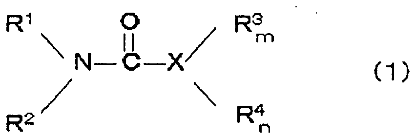
- a semiconductor device comprising a substrate, an adhesive layer, and a light emitting diode chip, in which the adhesive layer is a cured product of a die attach material, and the die attach material contains at least one resin component (A) selected from the group consisting of a compound (A1) represented by the following formula (1) and an acrylate compound (A2) which has a cycloalkylene group and two or more (meth) acrylic groups and does not have an aromatic ring in one molecule, at least one silane coupling agent (B) selected from the group consisting of a compound (B1) represented by the following formula (b-1) and a compound (B2) represented by the following formula (b-2), and an inorganic filler (C).
- R 1 , R 2 , R 3 , and R 4 each independently represent a hydrogen atom or an organic group not having an aromatic ring; at least two of R 1 , R 2 , R 3 , and R 4 each independently represent an organic group which has a (meth)acrylic group and does not have an aromatic ring; and at least two substituents of R 1 , R 2 , R 3 , and R 4 may form a ring.
- a die attach material which is used for attaching a substrate and a light emitting diode chip to each other, the material comprising: at least one resin component (A) selected from the group consisting of a compound (A1) represented by the formula (1) and an acrylate compound (A2) which has a cycloalkylene group and two or more (meth) acrylic groups and does not have an aromatic ring in one molecule; at least one silane coupling agent (B) selected from the group consisting of a compound (B1) represented by the following formula (b-1) and a compound (B2) represented by the following formula (b-2); and an inorganic filler (C).
- the die attach material be a die attach paste.
- the compound (A1) contain at least one selected from the group consisting of a compound represented by the following formula (a1-1) and a compound represented by the following formula (a1-2).
- R 1 , R 2 , and R 3 each independently represent a hydrogen atom or an organic group not having an aromatic ring; and at least two of R 1 , R 2 , and R 3 represent an organic group which has a (meth) acrylic group and does not have an aromatic ring.
- R 1' and R 2' each independently represent an organic group which has a (meth) acrylic group and does not have an aromatic ring.
- the compound (A1) be a compound having at least three acrylic groups or (meth) acrylic groups in the molecule.
- the acrylate compound (A2) contain a compound represented by the following formula (a2-1). (wherein R 1' and R 2' each independently represent an organic group which has a (meth) acrylic group and does not have an aromatic ring; R 11 and R 12 each independently represent a linear alkylene group or a single bond; and Z represents a cycloalkylene group.)
- the resin component (A) contain the compound represented by the formula (a1-1).
- silane coupling agent (B) contain the compound represented by the formula (b-1).
- Y represent a glycidyloxy group or a (meth)acryloyloxy group.
- a method for manufacturing a semiconductor device comprising: a step of preparing a die attach material by mixing at least one resin component (A) selected from the group consisting of a compound (A1) represented by the formula (1) and an acrylate compound (A2) which has a cycloalkylene group and two or more (meth) acrylic groups and does not have an aromatic ring in one molecule, at least one silane coupling agent (B) selected from the group consisting of a compound (B1) represented by the following formula (b-1) and a compound (B2) represented by the following formula (b-2), and an inorganic filler (C) with each other; a step of applying the die attach material to a substrate or a light emitting diode chip; and a step of attaching the light emitting diode chip to the substrate.
- the die attach material be a die attach paste.
- the compound (A1) contain at least one selected from the group consisting of a compound represented by the formula (a1-1) and a compound represented by the formula (a1-2).
- the compound (A1) be a compound having at least three acrylic groups or (meth) acrylic groups in the molecule.
- the acrylate compound (A2) contain a compound represented by the formula (a2-1).
- the resin component (A) contain the compound represented by the formula (a1-1).
- the silane coupling agent (B) contain the compound represented by the formula (b-1).
- Y represent a glycidyloxy group or a (meth)acryloyloxy group.
- a semiconductor device having a good balance between high light reflectivity, high color fastness, high elastic modulus, and high adhesive strength; and a method for manufacturing a semiconductor device can be provided.
- FIG. 1 is a cross-sectional view showing an example of a semiconductor device according to an embodiment of the present invention.
- a semiconductor device comprises a substrate, an adhesive layer, and a light emitting diode chip.
- the substrate is not particularly limited, and those used in an LED semiconductor device of the related art can be used.
- the substrate include frames in which a surface of copper, a copper alloy, a ceramic, an organic substrate, or the like is plated with silver, gold, a silver alloy, or the like to improve light reflectivity.
- a copper frame plated with silver is commonly used and is more preferable.
- FIG. 1 is a cross-sectional view showing an example of the semiconductor device according to the embodiment.
- the semiconductor device 10 comprises a substrate 1, a light emitting diode chip 3 that is mounted on the substrate 1, and an adhesive layer 2 that is provided between the substrate 1 and the light emitting diode chip 3.
- the substrate 1 and the light emitting diode chip 3 are electrically connected to each other through a bonding wire 20.
- the light emitting diode chip 3 and the bonding wire 20 are encapsulated with a transparent encapsulation resin 21.
- the adhesive layer contains a cured product of a die attach material containing the following components:
- the die attach material according to the embodiment may be a die attach film or a die attach paste. In addition, it is preferable that the die attach material according to the embodiment be a die attach paste.
- the die attach material according to the embodiment will be described using the die attach paste as an example.
- the (A) component is a resin component containing the (A1) component and/or the (A2) component.
- the (A1) component is a compound represented by the following formula (1).
- X represents an oxygen atom or a nitrogen atom
- R 1 , R 2 , R 3 , and R 4 each independently represent a hydrogen atom or an organic group not having an aromatic ring; at least two of R 1 , R 2 , R 3 , and R 4 each independently represent an organic group which has a (meth)acrylic group and does not have an aromatic ring; and at least two substituents of R 1 , R 2 , R 3 , and R 4 may form a ring.
- X represents an oxygen atom or a nitrogen atom
- m and n each independently represent 0 or 1.
- X represents an oxygen atom
- m+n 1
- X represents a nitrogen atom
- m+n 2. It is preferable that X represent a nitrogen atom.
- R 1 , R 2 , R 3 , and R 4 each independently represent a hydrogen atom or an organic group not having an aromatic ring. In this case, at least two of R 1 , R 2 , R 3 , and R 4 each independently represent an organic group which has a (meth)acrylic group and does not have an aromatic ring.
- Examples of the organic group of R 1 , R 2 , R 3 , and R 4 include organic groups derived from the following: a reactant between polyisocyanate not having an aromatic ring and a compound which does not have an aromatic ring and has one hydroxyl group and one or more (meth) acrylic groups in the molecule; a reactant between a compound which does not have an aromatic ring and has one isocyanate group and one or more (meth) acrylic groups in the molecule and polyol not having an aromatic ring; a reactant between polyisocyanate not having an aromatic ring and a compound which does not have an aromatic ring and has one amino group and one or more (meth) acrylic groups in the molecule; a reactant between a compound which does not have an aromatic ring and has one isocyanate group and one or more (meth) acrylic groups in the molecule and polyamine not having an aromatic ring; and a compound having a (meth) acrylic group in a substituent on a nitrogen atom of an isocyan
- polyisocyanate not having an aromatic ring examples include aliphatic diisocyanates, such as trimethylene diisocyanate, tetramethylene diisocyanate, hexamethylene diisocyanate, pentamethylene diisocyanate, 1,2-propylene diisocyanate, 2,3-butylene diisocyanate, 1, 3-butylene diisocyanate, dodecamethylene diisocyanate, and 2,4,4-trimethylhexamethylene diisocyanate; and alicyclic diisocyanates such as 3-isocyanatomethyl-3,5,5-trimethylcyclohexyl isocyanate (also known as isophorone diisocyanate), 1,3-cyclopentane diisocyanate, 1,3-cyclohexane diisocyanate, 1,4-cyclohexane diisocyanate, methyl-2,4-cyclohexane diisocyanate, methyl-2,6-cyclohexane di
- Examples of the compound which does not have an aromatic ring and has one hydroxyl group and one or more (meth) acrylic groups in the molecule include aliphatic (meth)acrylates having one hydroxyl group in the molecule such as 2-hydroxyethyl (meth)acrylate, 2-hydroxypropyl (meth)acrylate, 2-hydroxybutyl (meth)acrylate, 4-hydroxybutyl (meth)acrylate, and pentaerythritol tri(meth)acrylate; polyalkylene ether mono(meth)acrylates having one hydroxyl group in the molecule such as polyethylene glycol mono(meth)acrylate and poly(caprolactone) glycol mono(meth)acrylate; and polyester mono(meth)acrylates.
- aliphatic (meth)acrylates having one hydroxyl group in the molecule such as 2-hydroxyethyl (meth)acrylate, 2-hydroxypropyl (meth)acrylate, 2-hydroxybutyl (meth)acrylate, 4-hydroxybutyl (
- examples of the compound which does not have an aromatic ring and has one isocyanate group and one or more (meth)acrylic groups in the molecule include aliphatic acrylates having one isocyanate group and one or more (meth)acrylic groups in the molecule such as 2-(meth)acryloyloxy ethyl isocyanate, and 1,1-(bisacryloyloxy methyl)ethyl isocyanate.
- polyol not having an aromatic ring examples include aliphatic glycols such as ethylene glycol, propylene glycol, diethylene glycol, dipropylene glycol, butylene glycol, 1,6-hexanediol, 3-methyl-1,5-pentane glycol, neopentyl glycol, and hexane triol; aliphatic polyols such as trimethylolpropane and pentaerythritol; polyalkylene ether glycols such as polyethylene glycol; polyester glycols such as poly(caprolactone)glycol; and compounds having a hydroxyalkyl group in a substituent on a nitrogen atom of an isocyanurate ring such as tris(2-hydroxyethyl)isocyanurate.
- aliphatic glycols such as ethylene glycol, propylene glycol, diethylene glycol, dipropylene glycol, butylene glycol, 1,6-hexanediol
- polyamine not having an aromatic ring examples include aliphatic diamines such as trimethylene diamine, tetramethylene diamine, hexamethylene diamine, pentamethylene diamine, 1,2-propylenediamine, 2,3-butylenediamine, 1,3-butylenediamine, dodecamethylene diamine, and 2,4,4-trimethyl hexamethylene diamine; alicyclic diamines such as 3-aminomethyl-3,5,5-trimethyl cyclohexylamine (also known as isophorone diamine), 1,3-cyclopentanediamine, 1,3-cyclohexanediamine, 1,4-cyclohexanediamine, methyl-2,4-cyclohexanediamine, methyl-2,6-cyclohexanediamine, 4,4'-methylene bis(cyclohexylamine), 1,3-bis(aminomethyl)cyclohexane, and 1,4-bis(aminomethyl)cyclohexane; and alipha
- Examples of the compound having a (meth) acrylic group in a substituent on a nitrogen atom of an isocyanurate ring include (tris(2-hydroxyethyl)isocyanurate triacrylate, di(2-acryloyloxy ethyl)isocyanurate, and ⁇ -caprolactone-modified tris(2-acryloyloxy ethyl) isocyanurate, but the compounds are not limited thereto.
- the compounds of the present invention also include a compound into which a (meth)acrylic group is introduced by a condensation reaction between 2-hydroxyethyl isocyanurate or isocyanuric acid and (meth) acrylic acid or (meth) acrylic acid halide; and a compound in which a (meth)acrylic group is introduced, by a condensation reaction of (meth)acrylic acid or (meth)acrylic acid halide, into a terminal of a compound obtained by allowing a hydroxyl group of 2-hydroxyethyl isocyanurate, polyalkylene glycol, and polyester glycol to react with each other.
- tris (2-hydroxyethyl)isocyanurate triacrylate (SR-368, manufactured by Sartomer Company, Inc.), pentaerythritol triacrylate hexamethylene diisocyanate urethane prepolymer, pentaerythritol triacrylate hexamethylene diisocyanate urethane prepolymer (UA-306H, manufactured by Kyoeisha Chemical Co.
- pentaerythritol triacrylate isophorone diisosyanate urethane prepolymer U-306I, manufactured by Kyoeisha Chemical Co., Ltd.
- dipentaerythritol pentaacrylate hexamethylene diisocyanate urethane prepolymer U-510H, manufactured by Kyoeisha Chemical Co., Ltd.
- ⁇ -caprolactone-modified tris(2-acryloyloxy ethyl)isocyanurate (A-9300-1CL, manufactured by Shin-Nakamura Chemical Co., Ltd.), tris(2-acryloyloxy ethyl)isocyanurate, and di(2-acryloyloxy ethyl)isocyanurate are preferable.
- At least two substituents of R 1 , R 2 , R 3 , and R 4 may form a ring.
- X represent a nitrogen atom.
- the (A1) component contain at least one selected from the group consisting of a compound represented by the following formula (a1-1) and a compound represented by the following formula (a1-2), and it is particularly preferable that the (A1) component contain the compound represented by the following formula (a1-1).
- R 1 , R 2 , and R 3 each independently represent a hydrogen atom or an organic group not having an aromatic ring; and at least two of R 1 , R 2 , and R 3 represent an organic group which has a (meth) acrylic group and does not have an aromatic ring.
- R 1' and R 2' each independently represent an organic group which has a (meth) acrylic group and does not have an aromatic ring.
- R 1 , R 2 , and R 3 each independently represent a hydrogen atom or an organic group not having an aromatic ring and have the same definition as in the formula (1).
- the organic group of R 1 , R 2 , and R 3 a (meth) acryloyl group, a lactone-modified (meth)acryloyl group, a polyalkylene glycol (meth)acryloyl group are preferable; a (meth)acryloyl group and a lactone-modified (meth)acryloyl group are more preferable; and a (meth)acryloyl group is particularly preferable.
- At least two of R 1 , R 2 , and R 3 represent an organic group which has a (meth) acrylic group and does not have an aromatic ring, and it is preferable that all of R 1 , R 2 , and R 3 represent an organic group which has a (meth) acrylic group and does not have an aromatic ring.
- R 1' and R 2' each independently represent an organic group which has a (meth) acrylic group and does not have an aromatic ring and have the same definition as the organic group of R 1 , R 2 , and R 3 .
- the compound (A1) represented by the formula (1) be a compound having at least three acrylic groups or (meth) acrylic groups in the molecule.
- the compound (A1) represented by the formula (1) be a compound having at least three acrylic groups or (meth) acrylic groups in the molecule.
- the (A2) component is an acrylate compound which has a cycloalkylene group and two or more (meth)acrylic groups and does not have an aromatic ring in one molecule.
- the (A2) component be a compound represented by the following formula (a2-1). (wherein R 1' and R 2' each independently represent an organic group which has a (meth) acrylic group and does not have an aromatic ring; R 11 and R 12 each independently represent a linear alkylene group or a single bond; and Z represents a cycloalkylene group.)
- R 1' and R 2' each independently represent an organic group which has a (meth) acrylic group and does not have an aromatic ring and have the same definition as above.
- a (meth) acryloxy group, an alkyl (meth) acryloxy group, and a polyalkylene glycol (meth) acryloxy group are preferable; a (meth)acryloxy group and an alkyl (meth)acryloxy group are more preferable; and a (meth)acryloxy group is particularly preferable.
- R 11 and R 12 each independently represent a linear alkylene group or a single bond.
- Examples of the linear alkylene group of R 11 and R 12 include a methylene group, an ethylene group, and a trimethylene group.
- R 11 and R 12 a linear alkylene group is preferable, and it is particularly preferable that all of R 11 and R 12 represent a methylene group.
- Z represents a cycloalkylene group.
- the cycloalkylene group may be monocyclic or polycyclic but is preferably polycyclic.
- the number of carbon atoms in the cycloalkylene group is preferably more than or equal to 6, more preferably more than or equal to 8, and still more preferably more than or equal to 10.
- cycloalkylene group examples include a cyclopentylene group, a cyclohexylene group, and tricyclodecylene group.
- a cyclohexylene group and a tricyclodecylene group are preferable, and a tricyclodecylene group is particularly preferable.
- tricylodecane dimethanol diacrylate (A-DCP, manufactured by Shin-Nakamura Chemical Co. , Ltd.) can be used.
- the content of the resin component (A) contained in the die attach paste is preferably more than or equal to 3 wt% and less than or equal to 20 wt%, more preferably more than or equal to 5 wt% and less than or equal to 16 wt%, and still more preferably more than or equal to 7 wt% and less than or equal to 12 wt%.
- the reason is as follows. When the content of the resin component (A) is within the above-described range, high adhesive strength and high elastic modulus can be simultaneously realized, and defects are difficult to occur during wire bonding.
- the (B) component is at least one silane coupling agent selected from the group consisting of a (B1) component represented by the following formula (b-1) and/or a (B2) component represented by the following formula (b-2).
- R 5 , R 6 , and R 7 each independently represent an alkyl group having 1 to 10 carbon atoms or an alkoxy group having 1 to 10 carbon atoms. In this case, at least one of R 5 , R 6 , and R 7 represents an alkoxy group having 1 to 10 carbon atoms.
- the number of carbon atoms in the alkyl group of R 5 , R 6 , and R 7 is preferably 1 to 8, more preferably 1 to 5, and still more preferably 1 to 3.
- Specific examples of the alkyl group of R 5 , R 6 , and R 7 include a methyl group, an ethyl group, and a propyl group. Among these, a methyl group and an ethyl group are preferable, and a methyl group is particularly preferable.
- the number of carbon atoms in the alkoxy group of R 5 , R 6 , and R 7 is preferably 1 to 8, more preferably 1 to 5, and still more preferably 1 to 3.
- Specific examples of the alkoxy group of R 5 , R 6 , and R 7 include a methoxy group, an ethoxy group, a propoxy group, and a butoxy group. Among these, a methoxy group, an ethoxy group, and a propoxy group are preferable, and a methoxy group or an ethoxy group is particularly preferable.
- At least one of R 5 , R 6 , and R 7 represents an alkoxy group having 1 to 10 carbon atoms, and it is preferable that at least two of R 5 , R 6 , and R 7 represent an alkoxy group having 1 to 10 carbon atoms and it is particularly preferable that all of R 5 , R 6 , and R 7 represent an alkoxy group having 1 to 10 carbon atoms.
- Y represents any one of an amino group, a glycidyloxy group, a (meth)acryloyloxy group, a mercapto group, and an isocyanate group.
- Y an amino group, a glycidyloxy group, a (meth) acryloyloxy group, and a mercapto group are preferable, and a glycidyloxy group or a (meth)acryloyloxy group is particularly preferable.
- m and p each independently represent an integer of 1 to 10, preferably an integer of 1 to 6, and more preferably an integer of 1 to 3.
- n represents an integer of 1 or more, preferably an integer more than or equal to 2 and less than or equal to 10, and more preferably an integer more than or equal to 2 and less than or equal to 4.
- the (B) component be the (B1) component from the viewpoints of adhesive strength and reflectance.
- the content of the silane coupling agent (B) contained in the die attach paste is preferably more than or equal to 0.1 wt% and less than or equal to 10 wt%, more preferably more than or equal to 0. 5 wt% and less than or equal to 8 wt%, and still more preferably more than or equal to 1 wt% and less than or equal to 5 wt%.
- the reason is as follows. When the content of the silane coupling agent (B) is within the above-described range, high adhesive strength can be obtained, and adverse effects caused by voids or bleeding are difficult to occur.
- the (C) component is an inorganic filler.
- the inorganic filler is not particularly limited, and a well-known inorganic filler of the related art can be used.
- Specific examples of the inorganic filler include conductive fillers such as silver powder, gold powder, nickel powder, and copper powder; and insulating fillers such as aluminum nitride, calcium carbonate, silica, and alumina. These inorganic fillers can be used alone or in a combination of two or more kinds.
- a thermally conductive filler of 20 W/m ⁇ K or higher is preferably used because thermal conductivity is essential for use in a high-power LED.
- alumina, magnesia, boron nitride, and aluminum nitride are more preferably used, and alumina is particularly preferably used.
- the content of the inorganic filler (C) contained in the die attach paste is preferably more than or equal to 60 wt% and less than or equal to 90 wt%, more preferably more than or equal to 65 wt% and less than or equal to 85 wt%, and still more preferably more than or equal to 70 wt% and less than or equal to 80 wt%.
- the reason is as follows. When the content of the inorganic filler (C) is within the above-described range, high workability and thermal conductivity can be obtained.
- a well-known optional component of the related art can be further added to the die attach paste, in addition to the (A) component, the (B) component, and the (C) component.
- the optional component include an acrylate resin (hereinafter, referred to as "(D) component”) other than the (A) component and an organic peroxide (hereinafter, referred to as "(E) component").
- Examples of the acrylate resin as the (D) component include trimethylolpropane trimethacrylate, 2-(meth)acryloyloxyethyl succinic acid, 2-(meth)acryloyloxypropyl succinic acid, 2-(meth)acryloyloxyethyl hexahydrophthalic acid, 2-(meth)acryloyloxypropyl hexahydrophthalic acid, 2-(meth)acryloyloxyethyl methyl hexahydrophthalic acid, 2-(meth)acryloyloxypropyl methyl hexahydrophthalic acid, 2-(meth)acryloyloxyethyl phthalic acid, 2-(meth)acryloyloxypropyl phthalic acid, 2-(meth)acryloyloxyethyl phthalic acid, 2-(meth)acryloyloxypropyl phthalic acid, 2-(meth)acryloyloxyethyl tetra
- the acrylate resin is not limited to these examples. In addition, these acrylate resins may be used in a combination of two or more kinds from the viewpoints of curability, workability, adhesiveness, and the like.
- the acrylate resin (D) contained in the die attach paste is not an essential component. However, when it is necessary that viscosity, curability, and the like be adjusted, the content of the acrylate resin (D) is preferably more than or equal to 0.1 wt% and less than or equal to 20 wt%, more preferably more than or equal to 0.5 wt% and less than or equal to 15 wt%, and still more preferably more than or equal to 1 wt% and less than or equal to 10 wt%.
- Examples of the organic peroxide as the (E) component include 1,1-di(t-butylperoxy)cyclohexane, methyl ethyl ketone peroxide, methyl cyclohexanone peroxide, methyl acetoacetate peroxide, acetylacetone peroxide, 1,1-bis(t-butylperoxy)-3,3,5-trimethylcyclohexane, 1,1-bis(t-hexylperoxy) cyclohexane, 1,1-bis(t-hexylperoxy)-3,3,5-trimethyl cyclohexane, 1,1-bis(t-butylperoxy) cyclohexane, 2,2-bis(4,4-di-t-butylperoxy cyclohexyl)propane, 1,1-bis(t-butylperoxy)cyclododecane, n-butyl 4,4-bis(t-butylperoxy)valerate
- the content of the organic peroxide (E) contained in the die attach paste is preferably more than or equal to 0 wt% and less than or equal to 0.15 wt%, more preferably more than or equal to 0 wt% and less than or equal to 0.1 wt%, and still more preferably more than or equal to 0 wt% and less than or equal to 0.05 wt%.
- additives such as a curing agent, an organic solvent, a defoaming agent, a surfactant, and an elastomer can be used as desired.
- the die attach paste can be prepared, for example, by preliminarily mixing the respective components with each other, kneading a mixture thereof using a three-roll mill, and defoaming a kneaded product thereof in a vacuum.
- solid components be dissolved in an organic solvent before preliminary mixing.
- organic solvent examples include ethyl benzoate, propyl benzoate, butyl benzoate, ⁇ -butyrolactone, dibutyl oxalate, dimethyl maleate, diethyl maleate, ethylene glycol monobutyrate, propylene carbonate, N-methylpyrrolidone, 2-(hexyloxy)ethanol, diethylene glycol, diethylene glycol monoethyl ether, diethylene glycol monobutyl ether, triethyl glycol monomethyl ether, dipropylene glycol, tripropylene glycol monomethyl ether, methyl salicylate, diethylene glycol monoethyl ether acetate, and diethylene glycol monobutyl ether acetate.
- the die attach paste prepared as described above is applied to a substrate and a light emitting diode chip to attach the light emitting diode chip to the substrate.
- the semiconductor device according to the present embodiment can be manufactured.
- the die attach material according to the embodiment is a die attach film
- the die attach material is interposed between a substrate and a light emitting diode chip to attach the light emitting diode chip to the substrate.
- the semiconductor device according to the present embodiment can be manufactured.
- the semiconductor device according to the embodiment includes an adhesive layer that contains a cured product of the die attach paste having a good balance between high light reflectivity, high color fastness, high elastic modulus, and high adhesive strength. Therefore, the semiconductor device according to the embodiment can maximize light output and can maintain the maximum light output. In addition, in the semiconductor device according to the embodiment, even an extremely small LED chip can be attached to a substrate or the like without being detached during wire bonding.
- the die attach paste used in the adhesive layer of the semiconductor device according to the embodiment contains the (A1) component and/or the (A2) component as the resin component (A).
- the (A2) component does not have an aromatic ring, light absorption is low, and thus high light reflectance can be realized. Therefore, it is presumed that the light output of an LED can be maximized by using the maximum amount of light emitted from a light emitting diode chip to a substrate side.
- the (A2) component has a cycloalkylene group which is a more rigid skeleton and thus can realize high elastic modulus after curing.
- the resin component (A) is the compound represented by the formula (a1-1)
- the resin component (A) has the characteristics of both the (A1) component and the (A2) component. Therefore, a semiconductor device including an adhesive layer that contains a cured product of the die attach paste having a better balance between high light reflectivity, high color fastness, high elastic modulus, and high adhesive strength can be obtained.
- the die attach paste used in the adhesive layer of the semiconductor device according to the embodiment contains a specific silane coupling agent containing the (B1) component and/or the (B2) component.
- the (B1) component is a silane coupling agent containing any one of an amino group, a glycidyloxy group, a (meth)acryloyloxy group, a mercapto group, and an isocyanate group
- the (B2) component is a silane coupling agent having a sulfide bond.
- the silane coupling agent having a glycidyloxy group and a (meth) acryloyloxy group high adhesiveness can be imparted to the die attach paste, a varnish component of the die attach paste is not easily colored, and thus high light reflectance can be realized, which is preferable.
- Two or more kinds of silane coupling agents can be used in combination within a range where adhesiveness and light reflectivity do not deteriorate.
- each symbol represents the following meaning.
- the mixing amount of each component is represented by wt%.
- each component used in Examples and Comparative Examples is as described below.
- the die attach paste prepared in each of Examples and Comparative Examples was evaluated with the following method.
- a film-shaped test piece having a size of 6 ⁇ 3 ⁇ 0.1 mm was prepared (curing conditions: heating time of 30 minutes in a range of 25°C to 175°C and 30 minutes at 175°C), and the light reflectance at a wavelength of 450 nm was measured using a spectrophotometer (trade name: X-rite 8200, manufactured by S.D.G. K.K.).
- the light transmittance at a wavelength of 450 nm (T0) of a sheet-shaped cured product having a thickness of 1 mm (curing conditions: heating time of 30 minutes in a range of 25°C to 175°C and 30 minutes at 175°C) was measured using a spectrophotometer U-4100 (manufactured by Hitachi High-Technologies Corporation). After the cured product was irradiated with ultraviolet rays for 24 hours using an UV irradiating device (illuminance: 100 mW/cm 2 ) equipped with 365-nm band pass filter, the light transmittance (T1) thereof was measured with the same method as above to obtain T1/T0 (%).
- a silicon chip having a size of 0.5 ⁇ 0.5 mm was mounted on an Ag-plated copper frame, followed by curing in an oven under curing conditions of a heating time of 30 minutes in a range of 25°C to 175°C and 30 minutes at 175°C.
- the die shear strength of the cured product when being heated at 260°C was measured using an automated adhesive strength measuring device. During heating at 260°C, a die shear strength of 5 N or higher was evaluated as "A”, a die shear strength of higher than or equal to 3 N and lower than 5 N was evaluated as "B”, and a die shear strength of lower than 3 N was evaluated as "C”. The results are shown in Table 2.
- a film-shaped test piece having a size of 4 ⁇ 20 ⁇ 0.1 mm was prepared (curing conditions: heating time of 30 minutes in a range of 25°C to 175°C and 30 minutes at 175°C), and the elastic modulus thereof was measured using a dynamic viscoelasticity measuring device (DMA) in a pull mode. Measurement conditions were as follows.
- the die attach pastes of Examples 1 to 5 were superior in various properties required in an adhesive layer of a LED semiconductor device including reflectance (that is, light reflectivity), ultraviolet resistance (that is, high color fastness), elastic modulus, and adhesive strength; and that a practicable LED semiconductor device was able to be manufactured therefrom.
- all of the die attach pastes of Comparative Examples were not practically applicable to an LED semiconductor device.
- Example 1-3 Particularly in Example 1-3 in which the compound represented by the formula (a1-1) was used as the resin component (A), all the evaluation results were superior.
- the rigid cycloalkylene skeleton was provided, but a highly polar functional group was not provided. Therefore, high elastic modulus was able to be achieved, but slightly poor results were exhibited in adhesive strength as compared to Examples 1 to 3.
- Comparative Example 1 in which the epoxy resin was used as the resin component, it was found that reflectance and ultraviolet resistance were poor. The reason is presumed to be that the resin component of Comparative Example 1 contained an aromatic ring having a light absorbing ability in a visual light region and further contained a functional group which was easily oxidized.
- Comparative Example 3 in which the resin component (A) was not provided as the resin component, it was found that adhesive strength and elastic modulus were poor. The reason is presumed to be that the resin component of Comparative Example 3 did not have a highly polar functional group and a rigid structure such as a cycloalkylene skeleton.
Landscapes
- Chemical & Material Sciences (AREA)
- Organic Chemistry (AREA)
- Health & Medical Sciences (AREA)
- Chemical Kinetics & Catalysis (AREA)
- Medicinal Chemistry (AREA)
- Polymers & Plastics (AREA)
- Inorganic Chemistry (AREA)
- Adhesives Or Adhesive Processes (AREA)
- Die Bonding (AREA)
- Led Device Packages (AREA)
- Engineering & Computer Science (AREA)
- Microelectronics & Electronic Packaging (AREA)
Abstract
Description
- The present invention relates to a semiconductor device, a die attach material, and a method for manufacturing a semiconductor device.
- In recent years, light emitting diodes (LED) have been used as low-power LEDs (lower than 0.3 W/mK) or middle-power LEDs (0.3 W/mK to 0. 5 W/mK) in various fields such as backlights of mobile phones, fountain lights, spotlights, and liquid crystal display backlights of desktop computers and televisions. In addition, for the LEDs, further expansion of application fields including the use as high-power LEDs (higher than 0.5 W/mK) such as headlights of automobiles is expanded in the future.
- Typically, an LED is used as an LED package in which an LED chip is attached to a substrate or a lead frame, through a die attach paste.
- Various kinds of die attach pastes used in semiconductor devices are known in the related art (for example, refer to
Patent Documents 1 to 3). However, die attach pastes used in LEDs are required to have the following properties to maximize characteristics of LEDs. - This property is required to maximize light output of an LED by using the maximum amount of light emitted from the LED to a substrate side.
- This property is required to maintain the maximum output of an LED.
- This property is required because, in the case of a small LED chip, wire bonding cannot be performed at a low elastic modulus.
- This property is required for an LED chip not to be detached during wire bonding.
- As die attach pastes used in LEDs, those containing a silicone resin, an epoxy resin, an acrylic resin, or the like are currently known (for example, refer to Patent Documents 4 to 9).
- A die attach paste containing a silicone resin is superior due to its colorlessness and high color fastness but has a problem of low adhesiveness. A die attach paste containing an epoxy resin is superior in adhesiveness but is easily colored and has a problem of low color fastness. A die attach paste containing an acrylic resin is superior in light reflectivity but has problems of low adhesiveness and low elastic modulus.
-
- [Patent Document 1] Japanese Unexamined patent publication No.
2001-019912 - [Patent Document 2] Japanese Unexamined patent publication No.
2001-019722 - [Patent Document 3] Japanese Unexamined patent publication No.
2001-019821 - [Patent Document 4] Japanese Unexamined patent publication No.
2005-113059 - [Patent Document 5] Japanese Unexamined patent publication No.
2009-242587 - [Patent Document 6] Japanese Unexamined patent publication No.
2009-256400 - [Patent Document 7] Japanese Unexamined patent publication No.
2010-248349 - [Patent Document 8] Japanese Unexamined patent publication No.
2011-100927 - [Patent Document 9] Japanese Unexamined patent publication No.
2011-088947 - As a result of a study, the present inventors found that, when being applied to an LED as it is, a die attach paste for a semiconductor device of the related art is not suitably used from the viewpoint of high light reflectivity.
- In addition, one of die attach pastes for an LED of the related art is superior due to its colorlessness and high color fastness but has a problem of low adhesiveness, another one thereof is superior in adhesiveness but is easily colored and has a problem of low color fastness, and still another one thereof is superior in light reflectivity but has problems of low adhesiveness and low elastic modulus. Therefore, a die attach paste for an LED which satisfies all the properties (1) to (4) described above in "BACKGROUND ART" is not known.
- The present invention has been made in consideration of the above-described circumstances, and an object thereof is to provide a semiconductor device having a good balance between high light reflectivity, high color fastness, high elastic modulus, and high adhesive strength; and a method for manufacturing a semiconductor device.
- In order to solve the above-described problems, the present invention adopts the following configurations.
- That is, according to a first aspect of the present invention, there is provided a semiconductor device comprising a substrate, an adhesive layer, and a light emitting diode chip, in which the adhesive layer is a cured product of a die attach material, and the die attach material contains at least one resin component (A) selected from the group consisting of a compound (A1) represented by the following formula (1) and an acrylate compound (A2) which has a cycloalkylene group and two or more (meth) acrylic groups and does not have an aromatic ring in one molecule, at least one silane coupling agent (B) selected from the group consisting of a compound (B1) represented by the following formula (b-1) and a compound (B2) represented by the following formula (b-2), and an inorganic filler (C).

Y-(CH2)m-SiR5R6R7 (b-1)
(S)n-((CH2)p-SiR5R6R7)2 (b-2)
(wherein R5, R6, and R7 each independently represent an alkyl group having 1 to 10 carbon atoms or an alkoxy group having 1 to 10 carbon atoms; at least one of R5, R6, and R7 represents an alkoxy group having 1 to 10 carbon atoms; Y represents any one of an amino group, a glycidyloxy group, a (meth) acryloyloxy group, a mercapto group, and an isocyanate group; m and p each independently represent an integer of 1 to 10; and n represents an integer of 1 or more.) - In addition, according to a second aspect of the present invention, there is provided a die attach material which is used for attaching a substrate and a light emitting diode chip to each other, the material comprising: at least one resin component (A) selected from the group consisting of a compound (A1) represented by the formula (1) and an acrylate compound (A2) which has a cycloalkylene group and two or more (meth) acrylic groups and does not have an aromatic ring in one molecule; at least one silane coupling agent (B) selected from the group consisting of a compound (B1) represented by the following formula (b-1) and a compound (B2) represented by the following formula (b-2); and an inorganic filler (C).
- In the first and second aspects of the present invention, it is preferable that the die attach material be a die attach paste.
- In the first and second aspects of the present invention, it is preferable that the compound (A1) contain at least one selected from the group consisting of a compound represented by the following formula (a1-1) and a compound represented by the following formula (a1-2).


- In the first and second aspects of the present invention, it is preferable that the compound (A1) be a compound having at least three acrylic groups or (meth) acrylic groups in the molecule.
- In the first and second aspects of the present invention, it is preferable that the acrylate compound (A2) contain a compound represented by the following formula (a2-1).

- In the first and second aspects of the present invention, it is preferable that the resin component (A) contain the compound represented by the formula (a1-1).
- In the first and second aspects of the present invention, it is preferable that the silane coupling agent (B) contain the compound represented by the formula (b-1).
- In the first and second aspects of the present invention, it is preferable that, in the formula (b-1), Y represent a glycidyloxy group or a (meth)acryloyloxy group.
- According to a third aspect of the present invention, there is provided a method for manufacturing a semiconductor device, the method comprising: a step of preparing a die attach material by mixing at least one resin component (A) selected from the group consisting of a compound (A1) represented by the formula (1) and an acrylate compound (A2) which has a cycloalkylene group and two or more (meth) acrylic groups and does not have an aromatic ring in one molecule, at least one silane coupling agent (B) selected from the group consisting of a compound (B1) represented by the following formula (b-1) and a compound (B2) represented by the following formula (b-2), and an inorganic filler (C) with each other; a step of applying the die attach material to a substrate or a light emitting diode chip; and a step of attaching the light emitting diode chip to the substrate.
- In the third aspect of the present invention, it is preferable that the die attach material be a die attach paste.
- In the third aspect of the present invention, it is preferable that the compound (A1) contain at least one selected from the group consisting of a compound represented by the formula (a1-1) and a compound represented by the formula (a1-2).
- In the third aspect of the present invention, it is preferable that the compound (A1) be a compound having at least three acrylic groups or (meth) acrylic groups in the molecule.
- In the third aspect of the present invention, it is preferable that the acrylate compound (A2) contain a compound represented by the formula (a2-1).
- In the third aspect of the present invention, it is preferable that the resin component (A) contain the compound represented by the formula (a1-1).
- In the third aspect of the present invention, it is preferable that the silane coupling agent (B) contain the compound represented by the formula (b-1).
- In the third aspect of the present invention, it is preferable that, in the formula (b-1), Y represent a glycidyloxy group or a (meth)acryloyloxy group.
- According to the present invention, a semiconductor device having a good balance between high light reflectivity, high color fastness, high elastic modulus, and high adhesive strength; and a method for manufacturing a semiconductor device can be provided.
-
FIG. 1 is a cross-sectional view showing an example of a semiconductor device according to an embodiment of the present invention. - Hereinafter, embodiments of the present invention will be described with reference to the accompanying drawings. In all the drawings, like components are denoted by like reference, and the description thereof will not be repeated.
- A semiconductor device according to an embodiment of the present invention comprises a substrate, an adhesive layer, and a light emitting diode chip.
- The substrate is not particularly limited, and those used in an LED semiconductor device of the related art can be used.
- Specific examples of the substrate include frames in which a surface of copper, a copper alloy, a ceramic, an organic substrate, or the like is plated with silver, gold, a silver alloy, or the like to improve light reflectivity. Among these, a copper frame plated with silver is commonly used and is more preferable.
-
FIG. 1 is a cross-sectional view showing an example of the semiconductor device according to the embodiment. - For example, as shown in
FIG. 1 , thesemiconductor device 10 according to the embodiment comprises asubstrate 1, a light emitting diode chip 3 that is mounted on thesubstrate 1, and anadhesive layer 2 that is provided between thesubstrate 1 and the light emitting diode chip 3. In addition, in thesemiconductor device 10 according to the embodiment, thesubstrate 1 and the light emitting diode chip 3 are electrically connected to each other through abonding wire 20. The light emitting diode chip 3 and thebonding wire 20 are encapsulated with atransparent encapsulation resin 21. - In the semiconductor device according to the embodiment, the adhesive layer contains a cured product of a die attach material containing the following components:
- at least one resin component (A) (hereinafter, referred to as "(A) component") selected from the group consisting of a compound (A1) (hereinafter, referred to as "(A1) component") represented by the formula (1) and an acrylate compound (A2) (hereinafter, referred to as "(A2) component") which has a cycloalkylene group and two or more (meth)acrylic groups and does not have an aromatic ring in one molecule;
- at least one silane coupling agent (B) (hereinafter, referred to as "(B) component") selected from the group consisting of a compound (B1) (hereinafter, referred to as "(B1) component") represented by the formula (b-1) and a compound (B2) (hereinafter, referred to as "(B2) component") represented by the formula (b-2); and
- an inorganic filler (C) (hereinafter, referred to as " (C) component").
- Hereinafter, each component of the die attach material will be described.
- The die attach material according to the embodiment may be a die attach film or a die attach paste. In addition, it is preferable that the die attach material according to the embodiment be a die attach paste.
- Hereinafter, the die attach material according to the embodiment will be described using the die attach paste as an example.
- The (A) component is a resin component containing the (A1) component and/or the (A2) component.
- The (A1) component is a compound represented by the following formula (1).

- In the formula (1), X represents an oxygen atom or a nitrogen atom, and m and n each independently represent 0 or 1. In this case, when X represents an oxygen atom, m+n=1, and when X represents a nitrogen atom, m+n=2. It is preferable that X represent a nitrogen atom.
- In the formula (1), R1, R2, R3, and R4 each independently represent a hydrogen atom or an organic group not having an aromatic ring. In this case, at least two of R1, R2, R3, and R4 each independently represent an organic group which has a (meth)acrylic group and does not have an aromatic ring. Examples of the organic group of R1, R2, R3, and R4 include organic groups derived from the following: a reactant between polyisocyanate not having an aromatic ring and a compound which does not have an aromatic ring and has one hydroxyl group and one or more (meth) acrylic groups in the molecule; a reactant between a compound which does not have an aromatic ring and has one isocyanate group and one or more (meth) acrylic groups in the molecule and polyol not having an aromatic ring; a reactant between polyisocyanate not having an aromatic ring and a compound which does not have an aromatic ring and has one amino group and one or more (meth) acrylic groups in the molecule; a reactant between a compound which does not have an aromatic ring and has one isocyanate group and one or more (meth) acrylic groups in the molecule and polyamine not having an aromatic ring; and a compound having a (meth) acrylic group in a substituent on a nitrogen atom of an isocyanurate ring.
- Specific examples of the polyisocyanate not having an aromatic ring include aliphatic diisocyanates, such as trimethylene diisocyanate, tetramethylene diisocyanate, hexamethylene diisocyanate, pentamethylene diisocyanate, 1,2-propylene diisocyanate, 2,3-butylene diisocyanate, 1, 3-butylene diisocyanate, dodecamethylene diisocyanate, and 2,4,4-trimethylhexamethylene diisocyanate; and alicyclic diisocyanates such as 3-isocyanatomethyl-3,5,5-trimethylcyclohexyl isocyanate (also known as isophorone diisocyanate), 1,3-cyclopentane diisocyanate, 1,3-cyclohexane diisocyanate, 1,4-cyclohexane diisocyanate, methyl-2,4-cyclohexane diisocyanate, methyl-2,6-cyclohexane diisocyanate, 4,4'-methylene bis(cyclohexyl isocyanate), 1,3-bis(isocyanatomethyl)cyclohexane, 1,4-bis(isocyanatomethyl)cyclohexane, hydrogenated xylylene diisocyanate, and hydrogenated diphenylmethane diisocyanate.
- Examples of the compound which does not have an aromatic ring and has one hydroxyl group and one or more (meth) acrylic groups in the molecule include aliphatic (meth)acrylates having one hydroxyl group in the molecule such as 2-hydroxyethyl (meth)acrylate, 2-hydroxypropyl (meth)acrylate, 2-hydroxybutyl (meth)acrylate, 4-hydroxybutyl (meth)acrylate, and pentaerythritol tri(meth)acrylate; polyalkylene ether mono(meth)acrylates having one hydroxyl group in the molecule such as polyethylene glycol mono(meth)acrylate and poly(caprolactone) glycol mono(meth)acrylate; and polyester mono(meth)acrylates.
- Further, examples of the compound which does not have an aromatic ring and has one isocyanate group and one or more (meth)acrylic groups in the molecule include aliphatic acrylates having one isocyanate group and one or more (meth)acrylic groups in the molecule such as 2-(meth)acryloyloxy ethyl isocyanate, and 1,1-(bisacryloyloxy methyl)ethyl isocyanate.
- Examples of the polyol not having an aromatic ring include aliphatic glycols such as ethylene glycol, propylene glycol, diethylene glycol, dipropylene glycol, butylene glycol, 1,6-hexanediol, 3-methyl-1,5-pentane glycol, neopentyl glycol, and hexane triol; aliphatic polyols such as trimethylolpropane and pentaerythritol; polyalkylene ether glycols such as polyethylene glycol; polyester glycols such as poly(caprolactone)glycol; and compounds having a hydroxyalkyl group in a substituent on a nitrogen atom of an isocyanurate ring such as tris(2-hydroxyethyl)isocyanurate.
- Examples of the polyamine not having an aromatic ring include aliphatic diamines such as trimethylene diamine, tetramethylene diamine, hexamethylene diamine, pentamethylene diamine, 1,2-propylenediamine, 2,3-butylenediamine, 1,3-butylenediamine, dodecamethylene diamine, and 2,4,4-trimethyl hexamethylene diamine; alicyclic diamines such as 3-aminomethyl-3,5,5-trimethyl cyclohexylamine (also known as isophorone diamine), 1,3-cyclopentanediamine, 1,3-cyclohexanediamine, 1,4-cyclohexanediamine, methyl-2,4-cyclohexanediamine, methyl-2,6-cyclohexanediamine, 4,4'-methylene bis(cyclohexylamine), 1,3-bis(aminomethyl)cyclohexane, and 1,4-bis(aminomethyl)cyclohexane; and aliphatic polyamines such as spermine and spermidine.
- Examples of the compound having a (meth) acrylic group in a substituent on a nitrogen atom of an isocyanurate ring include (tris(2-hydroxyethyl)isocyanurate triacrylate, di(2-acryloyloxy ethyl)isocyanurate, and ε-caprolactone-modified tris(2-acryloyloxy ethyl) isocyanurate, but the compounds are not limited thereto. The compounds of the present invention also include a compound into which a (meth)acrylic group is introduced by a condensation reaction between 2-hydroxyethyl isocyanurate or isocyanuric acid and (meth) acrylic acid or (meth) acrylic acid halide; and a compound in which a (meth)acrylic group is introduced, by a condensation reaction of (meth)acrylic acid or (meth)acrylic acid halide, into a terminal of a compound obtained by allowing a hydroxyl group of 2-hydroxyethyl isocyanurate, polyalkylene glycol, and polyester glycol to react with each other.
- Among these, tris (2-hydroxyethyl)isocyanurate triacrylate (SR-368, manufactured by Sartomer Company, Inc.), pentaerythritol triacrylate hexamethylene diisocyanate urethane prepolymer, pentaerythritol triacrylate hexamethylene diisocyanate urethane prepolymer (UA-306H, manufactured by Kyoeisha Chemical Co. , Ltd.), pentaerythritol triacrylate isophorone diisosyanate urethane prepolymer (UA-306I, manufactured by Kyoeisha Chemical Co., Ltd.), dipentaerythritol pentaacrylate hexamethylene diisocyanate urethane prepolymer (UA-510H, manufactured by Kyoeisha Chemical Co., Ltd.), ε-caprolactone-modified tris(2-acryloyloxy ethyl)isocyanurate (A-9300-1CL, manufactured by Shin-Nakamura Chemical Co., Ltd.), tris(2-acryloyloxy ethyl)isocyanurate, and di(2-acryloyloxy ethyl)isocyanurate are preferable.
- In the formula (1), at least two substituents of R1, R2, R3, and R4 may form a ring. In this case, it is preferable that X represent a nitrogen atom.
- It is preferable that the (A1) component contain at least one selected from the group consisting of a compound represented by the following formula (a1-1) and a compound represented by the following formula (a1-2), and it is particularly preferable that the (A1) component contain the compound represented by the following formula (a1-1).


- In the formula (a1-1), R1, R2, and R3 each independently represent a hydrogen atom or an organic group not having an aromatic ring and have the same definition as in the formula (1). As the organic group of R1, R2, and R3, a (meth) acryloyl group, a lactone-modified (meth)acryloyl group, a polyalkylene glycol (meth)acryloyl group are preferable; a (meth)acryloyl group and a lactone-modified (meth)acryloyl group are more preferable; and a (meth)acryloyl group is particularly preferable.
- At least two of R1, R2, and R3 represent an organic group which has a (meth) acrylic group and does not have an aromatic ring, and it is preferable that all of R1, R2, and R3 represent an organic group which has a (meth) acrylic group and does not have an aromatic ring.
- In the formula (a1-2), R1' and R2' each independently represent an organic group which has a (meth) acrylic group and does not have an aromatic ring and have the same definition as the organic group of R1, R2, and R3. In the formula (a1-2), as the organic group of R1' and R2', organic groups derived from pentaerythritol triacrylate hexamethylene diisocyanate urethane prepolymer, pentaerythritol triacrylate toluene diisocyanate urethane prepolymer, pentaerythritol triacrylate isophorone diisocyanate urethane prepolymer, and dipentaerythritol pentaacrylate hexamethylene diisocyanate urethane prepolymer are preferable; organic groups derived from pentaerythritol triacrylate hexamethylene diisocyanate urethane prepolymer and pentaerythritol triacrylate isophorone diisocyanate urethane prepolymer are more preferable; and an organic group derived from pentaerythritol triacrylate hexamethylene diisocyanate urethane prepolymer is particularly preferable.
- In addition, it is preferable that the compound (A1) represented by the formula (1) be a compound having at least three acrylic groups or (meth) acrylic groups in the molecule. As a result, a semiconductor device having a better balance between high light reflectivity, high color fastness, high elastic modulus, and high adhesive strength can be realized.
- The (A2) component is an acrylate compound which has a cycloalkylene group and two or more (meth)acrylic groups and does not have an aromatic ring in one molecule.
- It is preferable that the (A2) component be a compound represented by the following formula (a2-1).

- In the formula (a2-1), R1' and R2' each independently represent an organic group which has a (meth) acrylic group and does not have an aromatic ring and have the same definition as above. In the formula (a2-1), as the organic group of R1' and R2', a (meth) acryloxy group, an alkyl (meth) acryloxy group, and a polyalkylene glycol (meth) acryloxy group are preferable; a (meth)acryloxy group and an alkyl (meth)acryloxy group are more preferable; and a (meth)acryloxy group is particularly preferable.
- In the formula (a2-1), R11 and R12 each independently represent a linear alkylene group or a single bond. Examples of the linear alkylene group of R11 and R12 include a methylene group, an ethylene group, and a trimethylene group.
- As R11 and R12, a linear alkylene group is preferable, and it is particularly preferable that all of R11 and R12 represent a methylene group.
- In the formula (a2-1), Z represents a cycloalkylene group. The cycloalkylene group may be monocyclic or polycyclic but is preferably polycyclic. The number of carbon atoms in the cycloalkylene group is preferably more than or equal to 6, more preferably more than or equal to 8, and still more preferably more than or equal to 10.
- Specific examples of the cycloalkylene group include a cyclopentylene group, a cyclohexylene group, and tricyclodecylene group. Among these, a cyclohexylene group and a tricyclodecylene group are preferable, and a tricyclodecylene group is particularly preferable.
- As such a compound, for example, tricylodecane dimethanol diacrylate (A-DCP, manufactured by Shin-Nakamura Chemical Co. , Ltd.) can be used.
- In the embodiment, the content of the resin component (A) contained in the die attach paste is preferably more than or equal to 3 wt% and less than or equal to 20 wt%, more preferably more than or equal to 5 wt% and less than or equal to 16 wt%, and still more preferably more than or equal to 7 wt% and less than or equal to 12 wt%. The reason is as follows. When the content of the resin component (A) is within the above-described range, high adhesive strength and high elastic modulus can be simultaneously realized, and defects are difficult to occur during wire bonding.
- The (B) component is at least one silane coupling agent selected from the group consisting of a (B1) component represented by the following formula (b-1) and/or a (B2) component represented by the following formula (b-2).
Y-(CH2)m-SiR5R6R7 (b-1)
(S)n-((CH2)p-SiR5R6R7)2 (b-2)
(wherein R5, R6, and R7 each independently represent an alkyl group having 1 to 10 carbon atoms or an alkoxy group having 1 to 10 carbon atoms; at least one of R5, R6, and R7 represents an alkoxy group having 1 to 10 carbon atoms; Y represents any one of an amino group, a glycidyloxy group, a (meth) acryloyloxy group, a mercapto group, and an isocyanate group; m and p each independently represent an integer of 1 to 10; and n represents an integer of 1 or more.) - In the formulae (b-1) and (b-2), R5, R6, and R7 each independently represent an alkyl group having 1 to 10 carbon atoms or an alkoxy group having 1 to 10 carbon atoms. In this case, at least one of R5, R6, and R7 represents an alkoxy group having 1 to 10 carbon atoms.
- The number of carbon atoms in the alkyl group of R5, R6, and R7 is preferably 1 to 8, more preferably 1 to 5, and still more preferably 1 to 3. Specific examples of the alkyl group of R5, R6, and R7 include a methyl group, an ethyl group, and a propyl group. Among these, a methyl group and an ethyl group are preferable, and a methyl group is particularly preferable.
- The number of carbon atoms in the alkoxy group of R5, R6, and R7 is preferably 1 to 8, more preferably 1 to 5, and still more preferably 1 to 3. Specific examples of the alkoxy group of R5, R6, and R7 include a methoxy group, an ethoxy group, a propoxy group, and a butoxy group. Among these, a methoxy group, an ethoxy group, and a propoxy group are preferable, and a methoxy group or an ethoxy group is particularly preferable.
- At least one of R5, R6, and R7 represents an alkoxy group having 1 to 10 carbon atoms, and it is preferable that at least two of R5, R6, and R7 represent an alkoxy group having 1 to 10 carbon atoms and it is particularly preferable that all of R5, R6, and R7 represent an alkoxy group having 1 to 10 carbon atoms.
- In the formula (b-1), Y represents any one of an amino group, a glycidyloxy group, a (meth)acryloyloxy group, a mercapto group, and an isocyanate group. Among these, as Y, an amino group, a glycidyloxy group, a (meth) acryloyloxy group, and a mercapto group are preferable, and a glycidyloxy group or a (meth)acryloyloxy group is particularly preferable.
- In the formulae (b-1) and (b-2), m and p each independently represent an integer of 1 to 10, preferably an integer of 1 to 6, and more preferably an integer of 1 to 3.
- In the formula (b-2), n represents an integer of 1 or more, preferably an integer more than or equal to 2 and less than or equal to 10, and more preferably an integer more than or equal to 2 and less than or equal to 4.
- In the embodiment, it is preferable that the (B) component be the (B1) component from the viewpoints of adhesive strength and reflectance.
- In the embodiment, the content of the silane coupling agent (B) contained in the die attach paste is preferably more than or equal to 0.1 wt% and less than or equal to 10 wt%, more preferably more than or equal to 0. 5 wt% and less than or equal to 8 wt%, and still more preferably more than or equal to 1 wt% and less than or equal to 5 wt%. The reason is as follows. When the content of the silane coupling agent (B) is within the above-described range, high adhesive strength can be obtained, and adverse effects caused by voids or bleeding are difficult to occur.
- The (C) component is an inorganic filler. The inorganic filler is not particularly limited, and a well-known inorganic filler of the related art can be used. Specific examples of the inorganic filler include conductive fillers such as silver powder, gold powder, nickel powder, and copper powder; and insulating fillers such as aluminum nitride, calcium carbonate, silica, and alumina. These inorganic fillers can be used alone or in a combination of two or more kinds. Among these, a thermally conductive filler of 20 W/m·K or higher is preferably used because thermal conductivity is essential for use in a high-power LED. In addition, when insulating properties are required along with thermal conductivity, alumina, magnesia, boron nitride, and aluminum nitride are more preferably used, and alumina is particularly preferably used.
- In the present invention, the content of the inorganic filler (C) contained in the die attach paste is preferably more than or equal to 60 wt% and less than or equal to 90 wt%, more preferably more than or equal to 65 wt% and less than or equal to 85 wt%, and still more preferably more than or equal to 70 wt% and less than or equal to 80 wt%. The reason is as follows. When the content of the inorganic filler (C) is within the above-described range, high workability and thermal conductivity can be obtained.
- In the embodiment, as desired, a well-known optional component of the related art can be further added to the die attach paste, in addition to the (A) component, the (B) component, and the (C) component. Specific examples of the optional component include an acrylate resin (hereinafter, referred to as "(D) component") other than the (A) component and an organic peroxide (hereinafter, referred to as "(E) component").
- Examples of the acrylate resin as the (D) component include trimethylolpropane trimethacrylate, 2-(meth)acryloyloxyethyl succinic acid, 2-(meth)acryloyloxypropyl succinic acid, 2-(meth)acryloyloxyethyl hexahydrophthalic acid, 2-(meth)acryloyloxypropyl hexahydrophthalic acid, 2-(meth)acryloyloxyethyl methyl hexahydrophthalic acid, 2-(meth)acryloyloxypropyl methyl hexahydrophthalic acid, 2-(meth)acryloyloxyethyl phthalic acid, 2-(meth)acryloyloxypropyl phthalic acid, 2-(meth)acryloyloxyethyl tetrahydrophthalic acid, 2-(meth)acryloyloxypropyl tetrahydrophthalic acid, 2-(meth)acryloyloxyethyl methyl tetrahydrophthalic acid, 2-(meth)acryloyloxypropyl methyl tetrahydrophthalic acid, 2-hydroxy-1,3-di(meth)acryloyloxypropane, tetramethylol methane tri(meth)acrylate, 2-hydroxyethyl (meth)acrylate, 2-hydroxypropyl (meth)acrylate, 2-hydroxybutyl (meth)acrylate, glycerin di(meth)acrylate, 2-hydroxy-3-(meth)acryloyloxypropyl (meth)acrylate, 1,4-cyclohexane dimethanol mono(meth)acrylate, ethyl-α-(hydroxymethyl) (meth)acrylate, 4-hydroxybutyl (meth)acrylate, methyl (meth)acrylate, ethyl (meth)acrylate, n-butyl (meth)acrylate, isobutyl (meth)acrylate, tert-butyl (meth)acrylate, isodecyl (meth)acrylate, lauryl (meth)acrylate, tridecyl (meth)acrylate, cetyl (meth)acrylate, stearyl (meth)acrylate, isoamyl (meth)acrylate, isostearyl (meth)acrylate, behenyl (meth)acrylate, 2-ethylhexyl (meth)acrylate, other alkyl (meth)acrylates, cyclohexyl (meth)acrylate, tert-butyl cyclohexyl (meth)acrylate, tetrahydrofurfuryl (meth)acrylate, benzyl (meth)acrylate, phenoxyethyl (meth)acrylate, isobornyl (meth)acrylate, glycidyl (meth)acrylate, trimethylolpropane tri(meth)acrylate, zinc mono(meth)acrylate, zinc di(meth)acrylate, dimethylaminoethyl (meth)acrylate, diethylaminoethyl (meth)acrylate, neopentyl glycol (meth)acrylate, trifluoroethyl (meth)acrylate, 2,2,3,3-tetrafluoropropyl (meth)acrylate, 2,2,3,3,4,4-hexafluorobutyl (meth)acrylate, perfluorooctyl (meth)acrylate, perfluorooctylethyl(meth)acrylate, ethyleneglycol di(meth)acrylate, propyleneglycol di(meth)acrylate, 1,4-butanediol di(meth)acrylate, 1,6-hexanediol di(meth)acrylate, 1,9-nonanediol di(meth)acrylate, 1,3-butanediol di(meth)acrylate, 1,10-decanediol di(meth)acrylate, tetramethyleneglycol di(meth)acrylate, methoxyethyl (meth)acrylate, butoxyethyl (meth)acrylate, ethoxydiethyleneglycol (meth)acrylate, methoxypolyalkyleneglycol mono(meth)acrylate, octoxypolyalkyleneglycol mono(meth)acrylate, lauroxypolyalkyleneglycol mono(meth)acrylate, stearoxypolyalkyleneglycol mono(meth)acrylate, allyloxypolyalkyleneglycol mono(meth)acrylate, nonylphenoxypolyalkyleneglycol mono(meth)acrylate, N,N'-methylene bis(meth)acrylic amide, N,N'-ethylene bis(meth)acrylic amide, 1,2-di(meth)acrylic amide ethyleneglycol, di(meth)acryloyloxymethyltricyclodecane, 2-(meth)acryloyloxyethyl, N-(meth)acryloyloxyethylmaleimide, N-(meth)acryloyloxyethylhexahydrophthalimide, N-(meth)acryloyloxyethylphthalimide, N-vinyl-2-pyrrolidone, ethoxylated bisphenol A (meth)acrylate, propoxylated bisphenol A (meth)acrylate, a styrene derivative, and a α-methylstyrene derivative. However, the acrylate resin is not limited to these examples. In addition, these acrylate resins may be used in a combination of two or more kinds from the viewpoints of curability, workability, adhesiveness, and the like. The acrylate resin (D) contained in the die attach paste is not an essential component. However, when it is necessary that viscosity, curability, and the like be adjusted, the content of the acrylate resin (D) is preferably more than or equal to 0.1 wt% and less than or equal to 20 wt%, more preferably more than or equal to 0.5 wt% and less than or equal to 15 wt%, and still more preferably more than or equal to 1 wt% and less than or equal to 10 wt%.
- Examples of the organic peroxide as the (E) component include 1,1-di(t-butylperoxy)cyclohexane, methyl ethyl ketone peroxide, methyl cyclohexanone peroxide, methyl acetoacetate peroxide, acetylacetone peroxide, 1,1-bis(t-butylperoxy)-3,3,5-trimethylcyclohexane, 1,1-bis(t-hexylperoxy) cyclohexane, 1,1-bis(t-hexylperoxy)-3,3,5-trimethyl cyclohexane, 1,1-bis(t-butylperoxy) cyclohexane, 2,2-bis(4,4-di-t-butylperoxy cyclohexyl)propane, 1,1-bis(t-butylperoxy)cyclododecane, n-butyl 4,4-bis(t-butylperoxy)valerate, 2,2-bis(t-butylperoxy)butane, 1,1-bis(t-butylperoxy)-2-methyl cyclohexane, t-butyl hydroperoxide, P-menthane hydroperoxide, 1,1,3,3-tetramethylbutyl hydroperoxide, t-hexyl hydroperoxide, dicumyl peroxide, 2,5-dimethyl-2,5-bis(t-butylperoxy)hexane, α,α'-bis(t-butylperoxy)diisopropyl benzene, t-butyl cumyl peroxide, di-t-butyl peroxide, 2,5-dimethyl-2,5-bis(t-butylperoxy)hexyne-3, isobutyryl peroxide, 3,5,5-trimethylhexanoyl peroxide, octanoyl peroxide, lauroyl peroxide, cinnamic acid peroxide, m-toluoyl peroxide, benzoyl peroxide, diisopropyl peroxydicarbonate, bis(4-t-butylcyclohexyl)peroxydicarbonate, di-3-methoxybutyl peroxydicarbonate, di-2-ethylhexyl peroxydicarbonate, di-sec-butyl peroxydicarbonate, di(3-methyl-3-methoxybutyl)peroxydicarbonate, di(4-t-butylcyclohexyl)peroxydicarbonate, α,α'-bis(neodecanoylperoxy)diisopropyl benzene, cumyl peroxyneodecanoate, 1,1,3,3-tetramethylbutyl peroxyneodecanoate, 1-cyclohexyl-1-methylethyl peroxyneodecanoate, t-hexyl peroxyneodecanoate, t-butyl peroxyneodecanoate, t-hexyl peroxypivalate, t-butyl peroxypivalate, 2,5-dimethyl-2,5-bis(2-ethylhexanoylperoxy)hexane, 1,1,3,3-tetramethyl butyl peroxy 2-ethyl hexanoate, 1-cyclohexyl-1-methyl ethyl peroxy-2-ethylhexanoate, t-hexylperoxy-2-ethylhexanoate, t-butyl peroxy-2-ethylhexanoate, t-butyl peroxyisobutyrate, t-butyl peroxymaleic acid, t-butylperoxy laurate, t-butylperoxy-3,5,5-trimethyl hexanoate, t-butyl peroxyisopropyl monocarbonate, t-butyl peroxy-2-ethylhexyl monocarbonate, 2,5-dimethyl-2,5-bis (benzoyl peroxy) hexane, t-butylperoxy acetate, t-hexylperoxy benzoate, t-butylperoxy-m-toluoyl benzoate, t-butylperoxy benzoate, bis(t-butylperoxy)isophthalate, t-butylperoxy allyl monocarbonate, and 3,3',4,4'-tetra(t-butyl peroxy carbonyl)benzophenone. These examples can be used alone or can be used in a combination of two or more kinds to control curability.
- The content of the organic peroxide (E) contained in the die attach paste is preferably more than or equal to 0 wt% and less than or equal to 0.15 wt%, more preferably more than or equal to 0 wt% and less than or equal to 0.1 wt%, and still more preferably more than or equal to 0 wt% and less than or equal to 0.05 wt%.
- In addition, in the die attach paste according to the embodiment, additives such as a curing agent, an organic solvent, a defoaming agent, a surfactant, and an elastomer can be used as desired.
- In the embodiment, the die attach paste can be prepared, for example, by preliminarily mixing the respective components with each other, kneading a mixture thereof using a three-roll mill, and defoaming a kneaded product thereof in a vacuum. In addition, it is preferable that solid components be dissolved in an organic solvent before preliminary mixing.
- Examples of the organic solvent include ethyl benzoate, propyl benzoate, butyl benzoate, γ-butyrolactone, dibutyl oxalate, dimethyl maleate, diethyl maleate, ethylene glycol monobutyrate, propylene carbonate, N-methylpyrrolidone, 2-(hexyloxy)ethanol, diethylene glycol, diethylene glycol monoethyl ether, diethylene glycol monobutyl ether, triethyl glycol monomethyl ether, dipropylene glycol, tripropylene glycol monomethyl ether, methyl salicylate, diethylene glycol monoethyl ether acetate, and diethylene glycol monobutyl ether acetate. Among these, ethyl benzoate, propyl benzoate, butyl benzoate, γ-butyrolactone, dibutyl oxalate, diethyl maleate, ethylene glycol monobutyrate, propylene carbonate, diethylene glycol, diethylene glycol monobutyl ether, triethyl glycol monomethyl ether, dipropylene glycol, tripropylene glycol monomethyl ether, methyl salicylate, diethylene glycol monoethyl ether acetate, and diethylene glycol monobutyl ether acetate are preferable, and γ-butyrolactone is more preferable.
- The die attach paste prepared as described above is applied to a substrate and a light emitting diode chip to attach the light emitting diode chip to the substrate. As a result, the semiconductor device according to the present embodiment can be manufactured. When the die attach material according to the embodiment is a die attach film, the die attach material is interposed between a substrate and a light emitting diode chip to attach the light emitting diode chip to the substrate. As a result, the semiconductor device according to the present embodiment can be manufactured.
- The semiconductor device according to the embodiment includes an adhesive layer that contains a cured product of the die attach paste having a good balance between high light reflectivity, high color fastness, high elastic modulus, and high adhesive strength. Therefore, the semiconductor device according to the embodiment can maximize light output and can maintain the maximum light output. In addition, in the semiconductor device according to the embodiment, even an extremely small LED chip can be attached to a substrate or the like without being detached during wire bonding.
- The reason why the above-described effects can be obtained is not clear but is presumed to be as follows.
- That is, the die attach paste used in the adhesive layer of the semiconductor device according to the embodiment contains the (A1) component and/or the (A2) component as the resin component (A).
- The (A1) component has a highly polar NC(=O) skeleton in the structure. Therefore, it is presumed that high adhesive strength can be realized.
- In addition, since the (A2) component does not have an aromatic ring, light absorption is low, and thus high light reflectance can be realized. Therefore, it is presumed that the light output of an LED can be maximized by using the maximum amount of light emitted from a light emitting diode chip to a substrate side. In addition, it is presumed that the (A2) component has a cycloalkylene group which is a more rigid skeleton and thus can realize high elastic modulus after curing.
- Particularly when the resin component (A) is the compound represented by the formula (a1-1), the resin component (A) has the characteristics of both the (A1) component and the (A2) component. Therefore, a semiconductor device including an adhesive layer that contains a cured product of the die attach paste having a better balance between high light reflectivity, high color fastness, high elastic modulus, and high adhesive strength can be obtained.
- In addition, the die attach paste used in the adhesive layer of the semiconductor device according to the embodiment contains a specific silane coupling agent containing the (B1) component and/or the (B2) component.
- The (B1) component is a silane coupling agent containing any one of an amino group, a glycidyloxy group, a (meth)acryloyloxy group, a mercapto group, and an isocyanate group, and the (B2) component is a silane coupling agent having a sulfide bond. Particularly, by the addition of the silane coupling agent having a glycidyloxy group and a (meth) acryloyloxy group, high adhesiveness can be imparted to the die attach paste, a varnish component of the die attach paste is not easily colored, and thus high light reflectance can be realized, which is preferable. Two or more kinds of silane coupling agents can be used in combination within a range where adhesiveness and light reflectivity do not deteriorate.
- Hereinafter, the present invention will be described in detail using examples but is not limited thereto.
- The respective components were mixed as shown in Table 1, were kneaded using a three-roll mill, and were defoamed to prepare a die attach paste.
[Table 1] Example Comparative Example 1 2 3 4 5 1 2 3 Resin Component (A) (A)-1 9.0 9.0 9.0 9.0 (A)-2 9.0 (A)-3 9.0 (A)-4 6.5 (A)-5 6.5 Silane Coupling Agent (B) (B)-1 3.0 3.0 3.0 3.0 6.5 4.4 (B)-2 3.0 (B)-3 3.0 Inorganic Filler (c) (C)-1 73.5 73.5 73.5 73.5 73.5 73.5 73.5 73.5 (C)-2 2.5 2.5 2.5 2.5 2.5 2.5 2.5 2.5 Acrylate Resin (D) (D)-1 3.0 3.0 3.0 3.0 3.0 3.0 17.5 (D)-2 1.5 1.5 1.5 1.5 1.5 1.5 2.2 Organic Peroxide (E) (E)-1 0.04 Curing Agent (F) (F)-1 3.9 (F)-2 0.4 Organic Solvent (S)-1 7.5 7.5 7.46 7.5 7.5 7.5 Catalyst (G)-1 0.2 - In Table 1, each symbol represents the following meaning. In addition, the mixing amount of each component is represented by wt%. In addition, each component used in Examples and Comparative Examples is as described below.
- (A)-1: tris (2-hydroxyethyl)isocyanurate triacrylate (trade name: SR-368, manufactured by Sartomer Company, Inc.)
- (A)-2: pentaerythritol triacrylate hexamethylene diisocyanate urethane prepolymer (trade name: UA-306H, manufactured by Kyoeisha Chemical Co., Ltd.)
- (A)-3: tricylodecane dimethanol diacrylate (trade name: A-DCP, manufactured by Shin-Nakamura Chemical Co., Ltd.)
- (A)-4: bisphenol F type epoxy resin (trade name: SB-403S, manufactured by Nippon Kayaku Co., Ltd.).
- (A)-5: m,p-cresyl glycidyl ether (trade name: m,p-CGE, manufactured by Sakamoto Yakuhin Kogyo Co., Ltd.)
-
- (B)-1: 3-glycidoxypropyl trimethoxysilane (trade name: KBM-403E, manufactured by Shin-Etsu Chemical Co., Ltd.)
- (B)-2: 3-methacryloxypropyl trimethoxysilane (trade name: KBM-503P, manufactured by Shin-Etsu Chemical Co. , Ltd.)
- (B)-3: 2-(3,4-epoxycyclohexyl)ethyl trimethoxysilane (trade name: KBM-303, manufactured by Shin-Etsu Chemical Co. , Ltd.)
-
- (C)-1: alumina (AX3-15R, manufactured by Nippon Steel Sumikin Materials Co., Ltd., average particle size: 3 µm)
- (C)-2: silylated silica (trade name: AEROSIL R805, manufactured by Nippon Aerosil Co., Ltd.)
- (D)-1: trimethylolpropane trimethacrylate (trade name: TMP, manufactured by Kyoeisha Chemical Co., Ltd.)
- (D)-2: a compound having tetraethylene glycol dimethacrylate as a major component (trade name: LIGHTESTER 4EG, manufactured by Kyoeisha Chemical Co., Ltd.)
-
- (E)-1: 1,1-di(t-butylperoxy)cyclohexane (trade name: PERHEXA C(S), manufactured by NOF Corporation).
- (F)-1: phenol novolac resin (trade name: PR-51470, manufactured by Sumitomo Bakelite Co., Ltd.)
- (F)-2: dicyandiamide (trade name: EH3636AS, manufactured by ADEKA Corporation)
- (S)-1: γ-butyrolactone
- (G)-1: tetraphenylphosphonium tetraphenylborate (trade name: TPP-K, manufactured by Hokko Chemical Industry Co., Ltd.)
- The die attach paste prepared in each of Examples and Comparative Examples was evaluated with the following method.
- A film-shaped test piece having a size of 6 × 3 × 0.1 mm was prepared (curing conditions: heating time of 30 minutes in a range of 25°C to 175°C and 30 minutes at 175°C), and the light reflectance at a wavelength of 450 nm was measured using a spectrophotometer (trade name: X-rite 8200, manufactured by S.D.G. K.K.).
- A reflectance of 60% or higher was evaluated as "A", and a reflectance of lower than 60% was evaluated as "B". The results are shown in Table 2.
- The light transmittance at a wavelength of 450 nm (T0) of a sheet-shaped cured product having a thickness of 1 mm (curing conditions: heating time of 30 minutes in a range of 25°C to 175°C and 30 minutes at 175°C) was measured using a spectrophotometer U-4100 (manufactured by Hitachi High-Technologies Corporation). After the cured product was irradiated with ultraviolet rays for 24 hours using an UV irradiating device (illuminance: 100 mW/cm2) equipped with 365-nm band pass filter, the light transmittance (T1) thereof was measured with the same method as above to obtain T1/T0 (%).
- A T1/T0 value of 90% or higher was evaluated as "A", and a T1/T0 value of lower than 90% was evaluated as "B". The results are shown in Table 2.
- A silicon chip having a size of 0.5 × 0.5 mm was mounted on an Ag-plated copper frame, followed by curing in an oven under curing conditions of a heating time of 30 minutes in a range of 25°C to 175°C and 30 minutes at 175°C. After curing, the die shear strength of the cured product when being heated at 260°C was measured using an automated adhesive strength measuring device. During heating at 260°C, a die shear strength of 5 N or higher was evaluated as "A", a die shear strength of higher than or equal to 3 N and lower than 5 N was evaluated as "B", and a die shear strength of lower than 3 N was evaluated as "C". The results are shown in Table 2.
- A film-shaped test piece having a size of 4×20×0.1 mm was prepared (curing conditions: heating time of 30 minutes in a range of 25°C to 175°C and 30 minutes at 175°C), and the elastic modulus thereof was measured using a dynamic viscoelasticity measuring device (DMA) in a pull mode. Measurement conditions were as follows.
- Measurement temperature: -100°C to 300°C
- Temperature increase rate: 5 °C/min
- Frequency: 10 Hz
- Load: 100 mN
- When the storage modulus at 200°C was obtained as the elastic modulus, an elastic modulus of 800 MPa was evaluated as "A", an elastic modulus of more than or equal to 400 MPa and less than 800 MPa was evaluated as "B", and an elastic modulus of less than 400 MPa was evaluated as "C". The results are shown in Table 2.
- Based on the above-described evaluation results, a die attach material which was practically applicable to an LED semiconductor device was evaluated as "A", and a die attach material which was not practically applicable to an LED semiconductor device was evaluated as "B". The results are shown in Table 2.
[Table 2] Example Comparative Example Evaluation Items 1 2 3 4 5 1 2 3 Reflectance A A A A A B A A Ultraviolet Resistance A A A A A B A A Adhesive Strength A A A A B A C C Elastic Modulus A A A B A A A C Comprehensive Evaluation A A A A A B B B - It was confirmed from the results of Table 2 that the die attach pastes of Examples 1 to 5 were superior in various properties required in an adhesive layer of a LED semiconductor device including reflectance (that is, light reflectivity), ultraviolet resistance (that is, high color fastness), elastic modulus, and adhesive strength; and that a practicable LED semiconductor device was able to be manufactured therefrom. In addition, all of the die attach pastes of Comparative Examples were not practically applicable to an LED semiconductor device.
- Particularly in Example 1-3 in which the compound represented by the formula (a1-1) was used as the resin component (A), all the evaluation results were superior. In the structure of the resin component of Example 4, the highly polar NC (=O) skeleton was provided, but a rigid structure was not provided. Therefore, high adhesive strength was able to be achieved, but slightly poor results were exhibited in elastic modulus as compared to Examples 1 to 3. In addition, in the structure of the resin component of Example 5, the rigid cycloalkylene skeleton was provided, but a highly polar functional group was not provided. Therefore, high elastic modulus was able to be achieved, but slightly poor results were exhibited in adhesive strength as compared to Examples 1 to 3.
- On the other hand, in Comparative Example 1 in which the epoxy resin was used as the resin component, it was found that reflectance and ultraviolet resistance were poor. The reason is presumed to be that the resin component of Comparative Example 1 contained an aromatic ring having a light absorbing ability in a visual light region and further contained a functional group which was easily oxidized.
- In addition, in Comparative Example 2 in which the silane coupling agent represented by the formula (b-3) was used, it was found that adhesiveness was poor although the compound represented by the formula (a1-1) was used as the resin component (A). The reason is presumed to be that, since the silane coupling agent used in Comparative Example 2 had a bulky reactive functional group compared to the coupling agent used in Examples, the reactivity of the resin composition was poor, a superior bond between the resin component and the inorganic filler or between the resin component and an adherend was not able to be obtained.
- In addition, in Comparative Example 3 in which the resin component (A) was not provided as the resin component, it was found that adhesive strength and elastic modulus were poor. The reason is presumed to be that the resin component of Comparative Example 3 did not have a highly polar functional group and a rigid structure such as a cycloalkylene skeleton.
- Hereinabove, the preferred embodiment of the present invention have been described, but the present invention is not limited to these embodiments. Within a range not departing from the scope of the present invention, additions, omissions, substitutions, and other modifications can be made for the configurations. The present invention is not limited the above description but is only limited to the accompanying claims.

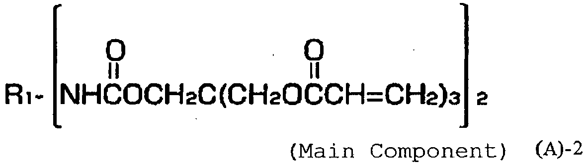


Claims (17)
- A semiconductor device comprising:a substrate;an adhesive layer; anda light emitting diode chip,wherein the adhesive layer is a cured product of a die attach material, andthe die attach material containsat least one resin component (A) selected from the group consisting of a compound (A1) represented by the following formula (1) and an acrylate compound (A2) which has a cycloalkylene group and two or more (meth) acrylic groups and does not have an aromatic ring in one molecule,at least one silane coupling agent (B) selected from the group consisting of a compound (B1) represented by the following formula (b-1) and a compound (B2) represented by the following formula (b-2), andan inorganic filler (C).
 (wherein X represents an oxygen atom or a nitrogen atom; m and n each independently represent 0 or 1; when X represents an oxygen atom, m+n=1; when X represents a nitrogen atom, m+n=2; R1, R2, R3, and R4 each independently represent a hydrogen atom or an organic group not having an aromatic ring; at least two of R1, R2, R3, and R4 each independently represent an organic group which has a (meth) acrylic group and does not have an aromatic ring; and at least two substituents of R1, R2, R3, and R4 may form a ring.)(wherein R5, R6, and R7 each independently represent an alkyl group having 1 to 10 carbon atoms or an alkoxy group having 1 to 10 carbon atoms; at least one of R5, R6, and R7 represents an alkoxy group having 1 to 10 carbon atoms; Y represents any one of an amino group, a glycidyloxy group, a (meth)acryloyloxy group, a mercapto group, and an isocyanate group; m and p each independently represent an integer of 1 to 10; and n represents an integer of 1 or more.)
Y-(CH2)m-SiR5R6R7 (b-1)
(S) n- ((CH2)p-SiR5R6R7)2 (b-2)
- The semiconductor device according to claim 1,
wherein the die attach material is a die attach paste. - The semiconductor device according to claim 1 or 2,
wherein the compound (A1) contains at least one selected from the group consisting of a compound represented by the following formula (a1-1) and a compound represented by the following formula (a1-2).

- The semiconductor device according to any one of claims 1 to 3,
wherein the compound (A1) is a compound having at least three acrylic groups or (meth)acrylic groups in the molecule. - The semiconductor device according to claim 1 or 2,
wherein the acrylate compound (A2) contains a compound represented by the following formula (a2-1).
- The semiconductor device according to claim 3,
wherein the resin component (A) contains the compound represented by the formula (a1-1). - The semiconductor device according to any one of claims 1 to 6,
wherein the silane coupling agent (B) contains the compound represented by the formula (b-1). - The semiconductor device according to any one of claims 1 to 7,
wherein in the formula (b-1), Y represents a glycidyloxy group or a (meth)acryloyloxy group. - A die attach material which is used for attaching a substrate and a light emitting diode chip to each other, the material comprising:at least one resin component (A) selected from the group consisting of a compound (A1) represented by the following formula (1) and an acrylate compound (A2) which has a cycloalkylene group and two or more (meth) acrylic groups and does not have an aromatic ring in one molecule;at least one silane coupling agent (B) selected from the group consisting of a compound (B1) represented by the following formula (b-1) and a compound (B2) represented by the following formula (b-2); andan inorganic filler (C).
 (wherein X represents an oxygen atom or a nitrogen atom; m and n each independently represent 0 or 1; when X represents an oxygen atom, m+n=1; when X represents a nitrogen atom, m+n=2; R1, R2, R3, and R4 each independently represent a hydrogen atom or an organic group not having an aromatic ring; at least two of R1, R2, R3, and R4 each independently represent an organic group which has a (meth) acrylic group and does not have an aromatic ring; and at least two substituents of R1, R2, R3, and R4 may form a ring.)(wherein R5, R6, and R7 each independently represent an alkyl group having 1 to 10 carbon atoms or an alkoxy group having 1 to 10 carbon atoms; at least one of R5, R6, and R7 represents an alkoxy group having 1 to 10 carbon atoms; Y represents any one of an amino group, a glycidyloxy group, a (meth)acryloyloxy group, a mercapto group, and an isocyanate group; m and p each independently represent an integer of 1 to 10; and n represents an integer of 1 or more.)
Y-(CH2)m-SiR5R6R7 (b-1)
(S)n-((CH2)p-SiR5R6R7)2 (b-2)
- A method for manufacturing a semiconductor device, the method comprising:a step of preparing a die attach material by mixing at least one resin component (A) selected from the group consisting of a compound (A1) represented by the following formula (1) and an acrylate compound (A2) which has a cycloalkylene group and two or more (meth) acrylic groups and does not have an aromatic ring in one molecule, at least one silane coupling agent (B) selected from the group consisting of a compound (B1) represented by the following formula (b-1) and a compound (B2) represented by the following formula (b-2), and an inorganic filler (C) with each other;a step of interposing the die attach material between a substrate and a light emitting diode chip; anda step of attaching the light emitting diode chip to the substrate.
 (wherein X represents an oxygen atom or a nitrogen atom; m and n each independently represent 0 or 1; when X represents an oxygen atom, m+n=1; when X represents a nitrogen atom, m+n=2; R1, R2, R3, and R4 each independently represent a hydrogen atom or an organic group not having an aromatic ring; at least two of R1, R2, R3, and R4 each independently represent an organic group which has a (meth) acrylic group and does not have an aromatic ring; and at least two substituents of R1, R2, R3, and R4 may form a ring.)(wherein R5, R6, and R7 each independently represent an alkyl group having 1 to 10 carbon atoms or an alkoxy group having 1 to 10 carbon atoms; at least one of R5, R6, and R7 represents an alkoxy group having 1 to 10 carbon atoms; Y represents any one of an amino group, a glycidyloxy group, a (meth)acryloyloxy group, a mercapto group, and an isocyanate group; m and p each independently represent an integer of 1 to 10; and n represents an integer of 1 or more.)
Y-(CH2)m-SiR5R6R7 (b-1)
(S)n-((CH2)p-SiR5R6R7)2 (b-2)
- The method for manufacturing a semiconductor device according to claim 10,
wherein the die attach material is a die attach paste, and in the step of interposing the die attach material, the die attach paste is applied to the substrate and the light emitting diode chip. - The method for manufacturing a semiconductor device according to claim 10 or 11,
wherein the compound (A1) contains at least one selected from the group consisting of a compound represented by the following formula (a1-1) and a compound represented by the following formula (a1-2).

- The method for manufacturing a semiconductor device according to any one of claims 10 to 12,
wherein the compound (A1) is a compound having at least three acrylic groups or (meth)acrylic groups in the molecule. - The method for manufacturing a semiconductor device according to claim 10 or 11,
wherein the acrylate compound (A2) contains a compound represented by the following formula (a2-1).
- The method for manufacturing a semiconductor device according to claim 12,
wherein the resin component (A) contains the compound represented by the formula (a1-1). - The method for manufacturing a semiconductor device according to any one of claims 10 to 15,
wherein the silane coupling agent (B) contains the compound represented by the formula (b-1). - The method for manufacturing a semiconductor device according to any one of claims 10 to 16,
wherein in the formula (b-1), Y represents a glycidyloxy group or a (meth)acryloyloxy group.
Applications Claiming Priority (2)
| Application Number | Priority Date | Filing Date | Title |
|---|---|---|---|
| JP2012089337 | 2012-04-10 | ||
| PCT/JP2013/002430 WO2013153803A1 (en) | 2012-04-10 | 2013-04-10 | Semiconductor device, die attaching material, and method for manufacturing semiconductor device |
Publications (2)
| Publication Number | Publication Date |
|---|---|
| EP2838126A1 true EP2838126A1 (en) | 2015-02-18 |
| EP2838126A4 EP2838126A4 (en) | 2015-10-28 |
Family
ID=49327387
Family Applications (1)
| Application Number | Title | Priority Date | Filing Date |
|---|---|---|---|
| EP13775725.8A Withdrawn EP2838126A4 (en) | 2012-04-10 | 2013-04-10 | SEMICONDUCTOR DEVICE, CHIP FASTENING MATERIAL, AND METHOD FOR MANUFACTURING SEMICONDUCTOR DEVICE |
Country Status (9)
| Country | Link |
|---|---|
| US (1) | US20150060889A1 (en) |
| EP (1) | EP2838126A4 (en) |
| JP (1) | JP6247204B2 (en) |
| KR (1) | KR20150003287A (en) |
| CN (1) | CN104221171B (en) |
| MY (1) | MY170959A (en) |
| SG (1) | SG11201405729QA (en) |
| TW (1) | TWI577767B (en) |
| WO (1) | WO2013153803A1 (en) |
Families Citing this family (6)
| Publication number | Priority date | Publication date | Assignee | Title |
|---|---|---|---|---|
| JP6356582B2 (en) * | 2014-11-25 | 2018-07-11 | 日東電工株式会社 | Adhesive sheet, adhesive sheet with dicing sheet, and method for manufacturing semiconductor device |
| JP6675155B2 (en) * | 2015-05-20 | 2020-04-01 | 京セラ株式会社 | Die attach paste for semiconductor and semiconductor device |
| JP6791626B2 (en) * | 2015-12-14 | 2020-11-25 | デクセリアルズ株式会社 | Manufacturing method of thermosetting adhesive sheet and semiconductor device |
| JP2018141106A (en) * | 2017-02-28 | 2018-09-13 | 住友ベークライト株式会社 | Thermosetting resin composition, resin sheet with carrier substrate and semiconductor device |
| KR102376144B1 (en) * | 2018-11-14 | 2022-03-18 | 주식회사 엘지화학 | Resin composition for bonding semiconductor, adhesive film for semiconductor, dicing diebonding film, and method for dicing of semiconductor wafer using the same |
| WO2020101236A1 (en) * | 2018-11-14 | 2020-05-22 | 주식회사 엘지화학 | Resin composition for semiconductor adhesion, semiconductor adhesive film using same, dicing die bonding film and semiconductor wafer dicing method |
Family Cites Families (20)
| Publication number | Priority date | Publication date | Assignee | Title |
|---|---|---|---|---|
| JPH09291259A (en) * | 1996-04-26 | 1997-11-11 | Sumitomo Bakelite Co Ltd | Low-temperature heating curable type anisotropic electroconductive adhesive |
| JP2000265119A (en) * | 1999-03-16 | 2000-09-26 | Sumitomo Bakelite Co Ltd | Die attach paste |
| JP3871828B2 (en) | 1999-07-05 | 2007-01-24 | 住友ベークライト株式会社 | Die attach paste and semiconductor device using the same |
| JP2001019722A (en) | 1999-07-05 | 2001-01-23 | Sumitomo Bakelite Co Ltd | Die attach paste and semiconductor device using the same |
| JP2001019912A (en) | 1999-07-05 | 2001-01-23 | Sumitomo Bakelite Co Ltd | Die attach paste and semiconductor device using the same |
| JP2002363218A (en) * | 2001-06-07 | 2002-12-18 | Hitachi Chem Co Ltd | Resin paste composition and semiconductor device using the same |
| JP2004266134A (en) * | 2003-03-03 | 2004-09-24 | Kanegafuchi Chem Ind Co Ltd | Resin paste for die bonding and light emitting diode using the same |
| JP4395350B2 (en) | 2003-10-09 | 2010-01-06 | 信越化学工業株式会社 | Curable resin composition and conductive adhesive |
| CN101123286A (en) * | 2006-08-09 | 2008-02-13 | 刘胜 | Light emitting diode packaging structure and method |
| JP5000259B2 (en) * | 2006-10-18 | 2012-08-15 | 株式会社ダイセル | Transparent sealing material |
| JP5070107B2 (en) | 2008-03-31 | 2012-11-07 | ナミックス株式会社 | Epoxy resin composition |
| JP2009256400A (en) | 2008-04-11 | 2009-11-05 | Shin Etsu Chem Co Ltd | Silicone adhesive for semiconductor element |
| JP5509738B2 (en) * | 2008-09-30 | 2014-06-04 | デクセリアルズ株式会社 | Acrylic insulating adhesive |
| JP5562574B2 (en) | 2009-04-14 | 2014-07-30 | 信越化学工業株式会社 | Thermally conductive adhesive |
| WO2010131575A1 (en) * | 2009-05-13 | 2010-11-18 | 日立化成工業株式会社 | Adhesive composition, adhesive sheet for connecting circuit member, and method for manufacturing semiconductor device |
| JP5246880B2 (en) * | 2009-09-15 | 2013-07-24 | 信越化学工業株式会社 | Underfill material composition and optical semiconductor device |
| JP5621236B2 (en) * | 2009-10-05 | 2014-11-12 | 日立化成株式会社 | Urethane resin composition, cured body, and optical semiconductor device using cured body |
| JP5544819B2 (en) | 2009-10-20 | 2014-07-09 | 住友金属鉱山株式会社 | Epoxy group-containing adhesive resin composition and optical semiconductor adhesive using the same |
| JP2011100927A (en) | 2009-11-09 | 2011-05-19 | Sony Chemical & Information Device Corp | Bonding agent composition |
| JP5812989B2 (en) * | 2010-05-21 | 2015-11-17 | 電気化学工業株式会社 | Composition and adhesive |
-
2013
- 2013-04-10 CN CN201380019303.1A patent/CN104221171B/en not_active Expired - Fee Related
- 2013-04-10 MY MYPI2014002800A patent/MY170959A/en unknown
- 2013-04-10 US US14/391,591 patent/US20150060889A1/en not_active Abandoned
- 2013-04-10 KR KR20147031367A patent/KR20150003287A/en not_active Abandoned
- 2013-04-10 WO PCT/JP2013/002430 patent/WO2013153803A1/en not_active Ceased
- 2013-04-10 TW TW102112698A patent/TWI577767B/en not_active IP Right Cessation
- 2013-04-10 JP JP2014510055A patent/JP6247204B2/en active Active
- 2013-04-10 SG SG11201405729QA patent/SG11201405729QA/en unknown
- 2013-04-10 EP EP13775725.8A patent/EP2838126A4/en not_active Withdrawn
Also Published As
| Publication number | Publication date |
|---|---|
| MY170959A (en) | 2019-09-20 |
| EP2838126A4 (en) | 2015-10-28 |
| TWI577767B (en) | 2017-04-11 |
| CN104221171B (en) | 2017-11-24 |
| JP6247204B2 (en) | 2017-12-13 |
| WO2013153803A1 (en) | 2013-10-17 |
| KR20150003287A (en) | 2015-01-08 |
| JPWO2013153803A1 (en) | 2015-12-17 |
| CN104221171A (en) | 2014-12-17 |
| SG11201405729QA (en) | 2014-11-27 |
| TW201345994A (en) | 2013-11-16 |
| US20150060889A1 (en) | 2015-03-05 |
Similar Documents
| Publication | Publication Date | Title |
|---|---|---|
| US20150060889A1 (en) | Semiconductor device, die attach material, and method for manufacturing semiconductor device | |
| US9243007B2 (en) | Organopolysiloxane, method for producing the same, and curable resin composition containing the organopolysiloxane | |
| KR100662176B1 (en) | Anisotropic conductive film composition | |
| KR101903819B1 (en) | Resin composition, semiconductor device using same, and method of manufacturing semiconductor device | |
| KR102686110B1 (en) | Manufacturing method of semiconductor device and adhesive film for semiconductor wafer processing | |
| KR102593694B1 (en) | Sheet for forming curable resin film and first protective film | |
| TWI445722B (en) | Electrical connection material between conductors and solar cell including the same | |
| CN110249414A (en) | Piece is used in curable resin film and the formation of the first protective film | |
| TWI580750B (en) | A heat-hardened conductive silicon oxide composition, a conductive adhesive composed of the composition, a conductive viscous material composed of the composition, an optical semiconductor device having a hardened material of the adhered material | |
| JP2011037981A (en) | Resin composition and semiconductor device produced using resin composition | |
| CN108260356B (en) | Curable resin film and 1 st protective film-forming sheet | |
| TW202509177A (en) | Encapsulating sheet and display | |
| KR20140027325A (en) | Semiconductor device | |
| KR102340593B1 (en) | Transparent resin composition, adhesive comprising composition, die bond material comprising composition, conductive connection method using composition, and optical semiconductor device obtained using method | |
| JP5482077B2 (en) | Resin composition and semiconductor device produced using resin composition | |
| JP2011057862A (en) | Resin composition and semiconductor device produced by using the same | |
| JP5476839B2 (en) | Resin composition and semiconductor device produced using resin composition | |
| CN111788275B (en) | Paste adhesive composition and semiconductor device | |
| JP5604828B2 (en) | Resin composition and semiconductor device produced using resin composition | |
| JP5589337B2 (en) | Manufacturing method of laminated structure | |
| KR20240029034A (en) | Adhesive film for circuit connection, circuit connection structure, and method of manufacturing the same | |
| KR102964365B1 (en) | Encapsulating sheet, display panel, and method for manufacturing display panel | |
| JP7796933B1 (en) | Encapsulating sheet and display having resin composition layer | |
| JP2020143246A (en) | Resin composition for wafer level optical semiconductor device, and optical semiconductor device | |
| JP7619513B1 (en) | Encapsulating sheet, display panel, and method for manufacturing display panel |
Legal Events
| Date | Code | Title | Description |
|---|---|---|---|
| PUAI | Public reference made under article 153(3) epc to a published international application that has entered the european phase |
Free format text: ORIGINAL CODE: 0009012 |
|
| 17P | Request for examination filed |
Effective date: 20141002 |
|
| AK | Designated contracting states |
Kind code of ref document: A1 Designated state(s): AL AT BE BG CH CY CZ DE DK EE ES FI FR GB GR HR HU IE IS IT LI LT LU LV MC MK MT NL NO PL PT RO RS SE SI SK SM TR |
|
| AX | Request for extension of the european patent |
Extension state: BA ME |
|
| DAX | Request for extension of the european patent (deleted) | ||
| RA4 | Supplementary search report drawn up and despatched (corrected) |
Effective date: 20150925 |
|
| RIC1 | Information provided on ipc code assigned before grant |
Ipc: H01L 33/48 20100101AFI20150921BHEP Ipc: C09J 4/02 20060101ALI20150921BHEP Ipc: H01L 33/56 20100101ALI20150921BHEP Ipc: H01L 23/00 20060101ALN20150921BHEP Ipc: C09J 11/04 20060101ALI20150921BHEP Ipc: C09J 11/06 20060101ALI20150921BHEP Ipc: C08F 2/44 20060101ALI20150921BHEP |
|
| STAA | Information on the status of an ep patent application or granted ep patent |
Free format text: STATUS: THE APPLICATION IS DEEMED TO BE WITHDRAWN |
|
| 18D | Application deemed to be withdrawn |
Effective date: 20160426 |