EP2835768A1 - Chip card and method for manufacturing such a chip card - Google Patents
Chip card and method for manufacturing such a chip card Download PDFInfo
- Publication number
- EP2835768A1 EP2835768A1 EP14178864.6A EP14178864A EP2835768A1 EP 2835768 A1 EP2835768 A1 EP 2835768A1 EP 14178864 A EP14178864 A EP 14178864A EP 2835768 A1 EP2835768 A1 EP 2835768A1
- Authority
- EP
- European Patent Office
- Prior art keywords
- layer
- face
- module
- cavity
- chip
- Prior art date
- Legal status (The legal status is an assumption and is not a legal conclusion. Google has not performed a legal analysis and makes no representation as to the accuracy of the status listed.)
- Withdrawn
Links
Images


Classifications
-
- G—PHYSICS
- G06—COMPUTING; CALCULATING OR COUNTING
- G06K—GRAPHICAL DATA READING; PRESENTATION OF DATA; RECORD CARRIERS; HANDLING RECORD CARRIERS
- G06K19/00—Record carriers for use with machines and with at least a part designed to carry digital markings
- G06K19/06—Record carriers for use with machines and with at least a part designed to carry digital markings characterised by the kind of the digital marking, e.g. shape, nature, code
- G06K19/067—Record carriers with conductive marks, printed circuits or semiconductor circuit elements, e.g. credit or identity cards also with resonating or responding marks without active components
- G06K19/07—Record carriers with conductive marks, printed circuits or semiconductor circuit elements, e.g. credit or identity cards also with resonating or responding marks without active components with integrated circuit chips
- G06K19/077—Constructional details, e.g. mounting of circuits in the carrier
- G06K19/07743—External electrical contacts
-
- G—PHYSICS
- G06—COMPUTING; CALCULATING OR COUNTING
- G06K—GRAPHICAL DATA READING; PRESENTATION OF DATA; RECORD CARRIERS; HANDLING RECORD CARRIERS
- G06K19/00—Record carriers for use with machines and with at least a part designed to carry digital markings
- G06K19/06—Record carriers for use with machines and with at least a part designed to carry digital markings characterised by the kind of the digital marking, e.g. shape, nature, code
- G06K19/067—Record carriers with conductive marks, printed circuits or semiconductor circuit elements, e.g. credit or identity cards also with resonating or responding marks without active components
- G06K19/07—Record carriers with conductive marks, printed circuits or semiconductor circuit elements, e.g. credit or identity cards also with resonating or responding marks without active components with integrated circuit chips
- G06K19/077—Constructional details, e.g. mounting of circuits in the carrier
- G06K19/07745—Mounting details of integrated circuit chips
- G06K19/07747—Mounting details of integrated circuit chips at least one of the integrated circuit chips being mounted as a module
-
- G—PHYSICS
- G06—COMPUTING; CALCULATING OR COUNTING
- G06K—GRAPHICAL DATA READING; PRESENTATION OF DATA; RECORD CARRIERS; HANDLING RECORD CARRIERS
- G06K19/00—Record carriers for use with machines and with at least a part designed to carry digital markings
- G06K19/06—Record carriers for use with machines and with at least a part designed to carry digital markings characterised by the kind of the digital marking, e.g. shape, nature, code
- G06K19/067—Record carriers with conductive marks, printed circuits or semiconductor circuit elements, e.g. credit or identity cards also with resonating or responding marks without active components
- G06K19/07—Record carriers with conductive marks, printed circuits or semiconductor circuit elements, e.g. credit or identity cards also with resonating or responding marks without active components with integrated circuit chips
- G06K19/077—Constructional details, e.g. mounting of circuits in the carrier
- G06K19/07718—Constructional details, e.g. mounting of circuits in the carrier the record carrier being manufactured in a continuous process, e.g. using endless rolls
Definitions
- the present invention relates to smart cards and the manufacture of such cards.
- the invention relates more particularly to the manufacture of smart cards comprising a module provided with a chip and contact pads, these contact pads being accessible by a device external to the card.
- the invention applies in particular, but not exclusively, to smart cards in accordance with the ISO 7816 standard.
- Such cards are for example used as bank cards, loyalty cards, access cards and so on. and can take various formats according to their respective use.
- Smart cards generally conform to a format whose dimensions are standardized.
- Credit cards for example, generally conform to the ISO ID-1 format defined by ISO 7816 (equivalent to the "1FF” (FF for "Form Factor”) format).
- SIM cards generally conform to the 2FF format (“Mini-SIM”), 3FF (“Micro-SIM”) or 4FF of the ISO 7816 standard.
- a smart card generally comprises a card body comprising an electronic chip capable of processing signals and performing various functions depending on the desired use of the card.
- Contact pads (or contact pads) electrically connected to the chip are formed on the surface of the card body so as to be accessible by an external reading device.
- the document US 4,222,516 proposes a method of manufacturing a smart card 100 provided with such contact pads.
- this document provides in particular the mounting in a card body 102 of a module 120, this module comprising a chip 124 and contacts 126 on the same face of a substrate 122.
- the module 120 is introduced into a cavity 108 arranged in the card body 102 so that the contacts 126 of the module 120 are vis-à-vis the through holes 110 formed beforehand in the upper layer 104 of the card body.
- the chip 124 is here fixed to the substrate 122 of the module 120, this substrate 122 being itself attached to a lower layer 106 of the card body so that the contacts 126 are visible through the through orifices 110.
- An external reading device can thus communicate with the chip 124 via the contact pads 126 accessible from the upper face 104 of the card 100.
- each contact pad must be arranged so that its free surface (on which must be made contact with an external device) is not more than 100 microns from the upper surface of the card body on which open the contact pads.
- the free face of the contact pads may be positioned recessed vis-à-vis the outer face of the card body (so as to form recesses) or protruding, as appropriate.
- the applicant has observed that the design of the 100 card proposed in the document US 4,222,516 is not optimal and does not allow in particular to control precisely the positioning of the free face of the contact pads 126 vis-à-vis the upper face 104a of the upper layer 104.
- the contact pads 126 of the module 120 do not engage in the corresponding orifices 110 but are simply positioned in alignment at the inlet of the orifices 110. This makes it difficult to comply with the ISO 7816 standard stipulating a maximum height difference of 100 ⁇ m.
- even a commitment would be made it would not be possible to precisely control the depth of engagement of the contact pads 126 in the corresponding orifices.
- the manufacturing method of the invention advantageously makes it possible to precisely control the difference in height that can exist between the external face of the first layer and the free surface of each contact pad once the module is in position on the internal face of the first layer.
- the invention thus makes it possible to improve the positioning of the contact pads with respect to the upper face (or front face) of the smart card, this positioning being critical to allow access under good conditions to an external device to the pads. contact card.
- the height positioning of the contact pads is in fact no longer dependent on variations in the thickness of the upper layer and / or positioning of the lower layer (or second layer) or an adhesive layer that can be between the layers upper and lower map body.
- the difference in height between the free surface of the contact pad and the outer face of the first layer is between 0 and 100 microns (in absolute value).
- the level difference between the contact surface of the pads and the front face of the card is between -100 ⁇ m and +100 ⁇ m as explained in more detail later.
- the free surface of at least one (or each) contact pad is flush with the outer face of the first layer.
- the contact pads are for example contact pads in accordance with the ISO 7816 standard.
- the card body comprises a second layer (or lower layer) extending on the inner face of the first layer, the first and second layers collectively defining a cavity in which the module is inserted.
- the first and second layers are two integral parts of the same part. These two layers are for example made together by molding.
- the closure means are formed by the third layer defined above in (b), the chip being covered with a coating resin formed on the second face of the module prior to insertion of the module into the cavity, the module being fixed (or maintained) to the third layer by means of an adhesive element disposed between the coating resin and the third layer.
- This particular variant makes it possible to form a link (or spacer) between the resin of the module encapsulating the chip and the third layer. This variant makes it possible to improve the resistance of the module to mechanical stresses such as pressure for example.
- the substrate of the module comprises a plurality of contact pads on its first face, each pad being engaged in a dedicated through hole of the first layer.
- the module substrate comprises a plurality of contact pads on its first face, the contact pads being adjacent to each other. to each other so that they are engaged in the same through hole of the first layer.
- each contact pad has a shape and dimensions complementary to the corresponding through hole.
- the module comprises an electronic component, such as a display, a fingerprint sensor or a light-emitting diode, disposed on the first face of the module, and wherein the first layer further comprises an additional orifice, the electronic component being inserted into the additional hole so as to be accessible from the first face of the card body. Once inserted in the additional orifice, the electronic component can thus be accessible visually or tactilely from the outer face of the card body.
- an electronic component such as a display, a fingerprint sensor or a light-emitting diode
- the difference in height between the free surface of the contact pad and the outer face of the first layer is between 0 and 100 microns (in absolute value).
- the level difference between the contact surface of the pads and the front face of the card is between -100 ⁇ m and +100 ⁇ m as explained in more detail later.
- the free surface of at least one (or each) contact pad is flush with the outer face of the first layer.
- the card body comprises a second layer extending on the inner face of the first layer, the method comprising the forming a cavity in said second layer, a portion of the inner face of the first layer forming the bottom of said cavity, fixing said module comprising inserting the module into the cavity and mounting the module on the bottom of the cavity.
- the first and second layers are two integral parts of the same part. These are for example made together by molding.
- each contact pad has a shape and dimensions complementary to the corresponding through hole.
- the closing step is carried out by fixing the third layer as defined above in (b), the chip being covered with a coating resin formed on the second face of the module beforehand. insertion into said cavity, the method further comprising depositing an adhesive member between the coating resin and the third layer so as to secure together the module and the third layer.
- this variant makes it possible to improve the resistance of the module to mechanical stresses such as pressure for example.
- the present invention relates to smart cards and the manufacture of such cards.
- the invention relates more particularly to the manufacture of smart cards comprising a module provided with a chip and contact pads, the latter being accessible by a device external to the card.
- a smart card 15 according to a first embodiment of the invention and an exemplary method of manufacturing such a card according to the invention are now described with reference to the Figures 2 to 5 .
- This first embodiment provides the supply (E2) of a card body 2. As indicated above, it will be assumed here that the card body 2 conforms to the ID-1 format, although other shapes and dimensions are possible ( figure 2 ).
- a cavity 8 is formed (E4) on the rear face 6a of the card body, this cavity being intended to receive a module 20 which will be described later.
- This cavity 8 can be performed by milling or any other suitable techniques.
- the card body 2 and the cavity 8 can be formed simultaneously by molding ( figure 2 ).
- the card body here comprises an upper layer 4 and a lower layer 6, these two layers extending against each other and collectively defining the cavity 8.
- the opening in the lower layer 6 delimits the edges of the cavity 8 while a portion 8b of the inner face 4b of the upper layer 4 forms the bottom of the cavity 8.
- the layers 4 and 6 may be two distinct layers fixed to one another by an appropriate method of attachment (gluing, lamination ...) of the inner face 4b of the first layer 4 on the inner face 6b of the second layer 6.
- the opening in the lower layer 6 defining the cavity 8 may be made before or after transfer to the first layer 4.
- the first layer may also delimit a portion of the edges of the cavity.
- the cavity 8 may have various shapes and dimensions as required, it being understood that the cavity must be able to accommodate a module as explained below. Although this is not mandatory, the cavity 8 here comprises a first recess 8a forming a step 8b on a peripheral portion of the cavity 8. The object of this step 8b will be described in more detail with reference to FIG. figure 5 .
- At least one through hole 10 is also formed (E6) in the portion of the inner face 4b forming the bottom 8b of the cavity 8 ( figure 2 ).
- Each orifice 10 is adapted to receive at least one contact pad 26 which will be described later. These contact pads are electrically conductive and allow the module to be brought into contact with an external device.
- the orifices 10 may be made by milling before or after the formation of the cavity 8.
- the card body 2, the cavity 8 and the orifices 10 may be formed simultaneously by molding.
- a module 20 is inserted (E8) in the cavity 8 and then fixed (E10) to the card body 2 to form a smart card 15.
- the module 20 comprises a substrate 22, the latter comprising at least one contact pad 26 on a first face 22b and a chip 24 on its opposite face 22a.
- the number and arrangement of the contact pads 26 of the module 20 are preferably adapted to the number and arrangement of the through-orifices 26 formed in the card body 2.
- the contact pads constitute contact pads in accordance with the ISO 7816 standard.
- the contact pads 26 are here of substantially rectangular shape, other forms being conceivable.
- the shape and the dimensions of the contact pads are complementary to those of their respective orifice.
- the module 20 has six contact pads on its first face 22b, these pads being configured to each be inserted into a dedicated hole 10 of the card body.
- an orifice 10 may be configured to receive a plurality of contact pads 26 disposed adjacent to each other on the first face 22b of the module.
- the chip 24 is here electrically connected to the contact pads 26, by means known to those skilled in the art, such as gold wires or by means for example of electrically conductive tracks formed in and / or on the substrate 22.
- the chip 24 may be covered with a coating resin (or encapsulation) 25 formed on the second face 22a of the module 20 prior to the insertion of the module 20 into the cavity 8.
- This resin 25 allows to improve the maintenance of the chip 24 on the substrate 22 of the module 20.
- the substrate and the chip 24 are completely received in the cavity 8, in the thickness of the lower layer 6 (or second layer 6) of the card body 2.
- This positioning of the substrate 22 and the chip 24 in the cavity 8 overcomes the variations in positioning of the lower layer, and thus allows more precise control of the positioning of the contact pads relative to the upper face of the chip card.
- the module 20 may comprise an antenna 28 on the second face 22a. This antenna is electrically connected to the chip and allows for example the implementation of RFID applications.
- step E8 the module 20 is inserted in the cavity 8 so that the first face 22b having the contact pads 26 is facing the bottom 8b of the cavity 8.
- the module 20 is thus fixed (E10) to the card body 2 so that the first face 22b of the module 20 is mounted in abutment against the inner face 4b (and more particularly against the cavity bottom 8b in the present case) of the first layer 4.
- This fixing is carried out so that each contact pad 26 engages in a respective through-orifice 10 so as to be accessible by an external device (not shown) from the first face 4a of the card body 2.
- the module 20 is bonded to the bottom of the cavity 8 by means of an adhesive layer 30, any other suitable fastening methods that can be envisaged within the scope of the invention.
- the first layer 4 has a thickness e being, for example approximately equal to 80 microns.
- the contact pads 26 have a thickness e2 of for example between 30 and 80 microns, other values being however possible according to the needs.
- the contact pads 26 are inserted into respective through holes 10 of the first layer 4 so as to be accessible from the outer face 4a of the first face 4.
- the manufacturing method of the invention advantageously makes it possible to accurately control the difference in height h1 (ie the distance along the longitudinal axis of the orifices) that can exist between the outer face 4a of the first layer 4 and the free surface 26a of each stud 26 once the module 20 in position on the inner face 4b of the first layer 4.
- This gap of level h1 may be negative (ie the contact pad 26 is then recessed in the orifice 10 vis-à-vis the outer face 4a so as to form a recess on the surface of the card 15, as shown in Figure 4A ) or positive (ie the contact pad 26 then extends through the orifice 10 so as to form a projection on the surface of the card 15).
- this difference h1 is between -100 ⁇ m and +100 ⁇ m (i.e. a difference of less than or equal to 100 ⁇ m in absolute value) in accordance with the ISO 7816 standard.
- the Figure 4B represents a particular variant embodiment according to which the difference in height h1 is zero (or approximately zero) so that the free surface 26a of the contact pad 26 considered is flush with the external face 4a of the first layer 4. In a particular case, the free surface 26a of each contact pad 26 is flush with the outer surface 4a.
- the cavity 8 opens on the outer face 6a of the second layer 6, that is to say on the face of the second layer 6 opposite to the inner face 4b of the first layer 4.
- closing of the cavity 8 is carried out (E12) by means of a closure layer 35 (made of plastic for example) which is fixed on the outer face 6a of the second layer (or on a peripheral portion of the cavity 8) so as to cover the cavity 8.
- the closure layer 35 is fixed on the peripheral portion 8a of the cavity 8 by means of an adhesive strip 38.
- This closure layer 35 is preferably fixed so as to be flush with the external face 6a of the second layer 6.
- the alignment of the levels of the external face 6a and of the closure layer 35 is achieved by adjusting the depth of the first step 8a, the thickness of the adhesive layer 38 and the thickness of the closure layer 35.
- an adhesive member 27 between the sealing resin 25 and the sealing layer 35 so as to fix together the module 20 and the sealing layer 35.
- the adhesive member 27 may be a drop of glue (or any other appropriate adhesive) deposited for example at the top of the coating resin 25 covering the chip 24.
- the closure layer 35 is then laminated on the outer face of the lower layer 6 of the card body so as to enter contact with the drop of glue 27.
- this adhesive element 27 is optional but advantageously makes it possible to form a link (or spacer) between the module 20 and the closure layer 35. This variant makes it possible to improve the resistance of the module 20 to mechanical stresses such as the pressure .
- the closing of the cavity 8 is performed (E12) by means of an electronic device (or component) (not shown) which is fixed on the outer face 6a of the second layer 6 (or on a peripheral portion of the cavity 8 ) similarly to the closure layer 35 shown in FIG. figure 5 so as to cover the cavity 8.
- This electronic device may be an LCD screen for example or a battery, this device being fixed by means for example of the adhesive layer 38.
- the electrical connection between the module 20 and the electrical device is for example provided by means of an extra thickness formed in the cavity 8 and taking the form of at least one "bump" (ie metal alloy element comprising conductive tracks), this bump being in contact with a portion of the inner face of the electrical device on the one hand, and with a portion of the second face 22a of the module 20 on the other hand.
- bump metal alloy element comprising conductive tracks
- cavity 8 is devoid of the step 8a and the closure layer is fixed directly on the rear face of the card body.
- a resin 40 of low viscosity eg of polyurethane
- a resin 40 of molding this resin being injected (E14) so as to cover the entire module 20 ( figure 6 ).
- the module 20 comprises, even before it is inserted into the cavity 8, a molded resin layer 44 ("Transfer molding resin") covering all of the second face 22a of the substrate 22.
- the cavity is devoid of the step 8a.
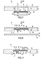
- the figure 8 represents yet another alternative according to which an additional layer 50 is fixed (E18) by lamination over the entire outer face 6a of the second layer 6.
- This layer 50 may comprise an underlayer 52 (of plastic for example) on which is disposed a suitable adhesion layer 54, namely a hot-pressable layer in the present case (the use of a cold-melt adhesive layer or "adhesive cold melt” is also possible).
- the adhesion layer 52 is located at the bonding interface between the outer face 6a and the additional layer 52.
- an adhesive element (not shown) between the resin of coating 25 and the adhesion layer 54 in a similar manner to the addition of the adhesive element 27 mentioned above with reference to the figure 5 .
- the module comprises at least one electronic component 32, such as a display, a cavity sensor or a light-emitting diode, disposed on the first face 22b of the module 20 and the first layer 4 further comprises an additional orifice 34 adapted to receiving the electronic component 32.
- the electronic component 32 is inserted into the additional orifice 34 so as to be accessible visually or tactilely from the outer face 4a of the card body 2.
- the component 32 represented in figure 11 passes through the additional orifice 34 so as to form a protrusion extending from the outer surface 4a of the card body 2.
- the card body 2 may comprise a dedicated additional orifice for each electronic component 32 disposed on the first face 22b of the module 20 or, alternatively, the same additional orifice may be configured to simultaneously receive several components. electronic 32.
- the cavity in which the module is inserted may be a non-emergent cavity.
- the first layer and the second layer are for example assembled to each other so as to receive in the non-emergent cavity the module according to the invention.
- the substrate can be plane.
- the substrate is completely received in the cavity, in the thickness of the second layer of the card body.
- first layer 4 and / or the second layer 6 may be plastic.
- a coil 58 of plastic sheets is unwound progressively to a first milling (or cutting) station where patterns 60 are made (E28) by means of a milling (or cutting) device 59. Then the sheets with these patterns are successively transported to the various operational positions responsible for performing the successive manufacturing steps E30 to E38.
- the patterns 60 comprise a cavity opening (or recess) 70 at the bottom of which are formed through orifices 72 ( figure 10 ).
- a module 20 is inserted (by means of a "pick and place” device) into the cavity 70 provided for this purpose so that each contact pad present on the first face of the module substrate engages in one of the through holes 72.
- the formation of the cavity 70 is performed before the fixing of the module 20.
- a hot pressure is then applied (E32) by means of a press 64 on the second face of the module comprising the chip 24.
- This adhesion layer is activated (E36) subsequently by lamination by means of a device 66.
- the module 20 is thus introduced into the cavity 70 before carrying out a lamination.
- a card punching step E38 is then performed in order to cut the smart cards according to the desired format.
- the module in the sense of the invention is attached to the card body so that the first face of said module is mounted in abutment against the inner face of the first layer (where appropriate at the bottom of the card). a cavity made for this purpose).
- This fixation is carried out so that each contact pad engages in a respective through hole so as to be accessible by an external device from the first face of the card body.
- an external device is for example a bank card reading terminal.
- Access to the contact pads is done for example by means of contact pins which is provided with the external device, these pins being configured to come into contact with the free surface of the contact pads.
- the manufacturing method of the invention advantageously makes it possible to precisely control the difference in height that can exist between the external face of the first layer and the free surface of each stud once the module is in position on the internal face of the first layer.
- the invention thus makes it possible to improve the positioning of the contact pads with respect to the upper face of the smart card, this positioning being critical to allow access under good conditions to a device external to the contact pads of the card.
- the height positioning of the contact pads is in fact no longer dependent on variations in the thickness of the upper layer and / or in positioning of the lower layer or the thickness of an adhesive layer that can be between the upper layers and bottom of the card body.
- the present invention also serves to protect the module in the card body and engage the contact pads in the orifices provided for this purpose without the shape or the module contour is apparent in relief on the front face ( touch pad side) of the smart card (see the 105 relief in figure 1 ). The aesthetics is thus improved and the module is less exposed to external shocks.
Abstract
L'invention concerne une carte à puce (15) comprenant : - un module (20) comportant un substrat (22) comprenant au moins un plot de contact (26) sur une première face (22b) du substrat et une puce (24) montée sur une deuxième face (22a) du substrat, la puce (24) étant reliée électriquement au plot de contact (26) ; et - un corps de carte comportant au moins une première couche (4) délimitée par une face externe (4a) et une face interne (4b) ; dans laquelle : - la première couche (4) comporte au moins un orifice traversant (10) adapté pour recevoir au moins un dit plot de contact (26) ; et - le module (20) est fixé au corps de carte de sorte que la première face (22b) du module est montée en appui contre la face interne (4b) de la première couche (4), ledit au moins un plot de contact (26) étant engagé dans l'orifice (10) de façon à être accessible par un dispositif externe depuis la première face (4a) du corps de carte.The invention relates to a chip card (15) comprising: a module (20) comprising a substrate (22) comprising at least one contact pad (26) on a first face (22b) of the substrate and a chip (24) mounted on a second face (22a) of the substrate, the chip (24) being electrically connected to the contact pad (26); and - a card body having at least a first layer (4) defined by an outer face (4a) and an inner face (4b); in which : - The first layer (4) comprises at least one through hole (10) adapted to receive at least one said contact pad (26); and the module (20) is fixed to the card body so that the first face (22b) of the module is mounted in abutment against the inner face (4b) of the first layer (4), said at least one contact pad ( 26) being engaged in the orifice (10) so as to be accessible by an external device from the first face (4a) of the card body.
Description
La présente invention concerne les cartes à puce ainsi que la fabrication de telles cartes. L'invention porte plus particulièrement sur la fabrication de cartes à puce comprenant un module muni d'une puce et de plots de contact, ces plots de contact étant accessibles par un dispositif externe à la carte.The present invention relates to smart cards and the manufacture of such cards. The invention relates more particularly to the manufacture of smart cards comprising a module provided with a chip and contact pads, these contact pads being accessible by a device external to the card.
L'invention s'applique notamment, mais de façon non exclusive, aux cartes à puce conformes au standard ISO 7816.The invention applies in particular, but not exclusively, to smart cards in accordance with the ISO 7816 standard.
L'utilisation des cartes à puce est aujourd'hui largement répandue dans la vie quotidienne. De telles cartes sont par exemple utilisées comme cartes bancaires, cartes de fidélité, cartes d'accès etc. et peuvent prendre divers formats selon leur utilisation respective.The use of smart cards is now widespread in everyday life. Such cards are for example used as bank cards, loyalty cards, access cards and so on. and can take various formats according to their respective use.
Les cartes à puce respectent généralement un format dont les dimensions sont normalisées. Les cartes de crédit, par exemple, sont généralement conformes au format ISO ID-1 défini par la norme ISO 7816 (équivalent au format « 1FF » (FF pour « Form Factor »)). Les cartes SIM sont quant à elles généralement conformes au format 2FF (« Mini-SIM »), 3FF (« Micro-SIM ») ou 4FF de la norme ISO 7816.Smart cards generally conform to a format whose dimensions are standardized. Credit cards, for example, generally conform to the ISO ID-1 format defined by ISO 7816 (equivalent to the "1FF" (FF for "Form Factor") format). SIM cards generally conform to the 2FF format ("Mini-SIM"), 3FF ("Micro-SIM") or 4FF of the ISO 7816 standard.
De façon connue, une carte à puce comprend généralement un corps de carte comportant une puce électronique apte à traiter des signaux et à réaliser divers fonctions selon l'utilisation souhaitée de la carte. Des plots de contact (ou plage de contact) reliés électriquement à la puce sont ménagés à la surface du corps de carte de façon à être accessibles par un dispositif de lecture externe.In known manner, a smart card generally comprises a card body comprising an electronic chip capable of processing signals and performing various functions depending on the desired use of the card. Contact pads (or contact pads) electrically connected to the chip are formed on the surface of the card body so as to be accessible by an external reading device.
Le document
Un dispositif de lecture externe peut ainsi communiquer avec la puce 124 via les plots de contact 126 accessibles depuis la face supérieure 104 de la carte 100.An external reading device can thus communicate with the
Cependant, la norme ISO 7816 impose à présent que la différence de hauteur entre la face libre des plots de contact et la face supérieure du corps de carte soit comprises entre 0 et 100 µm. Autrement dit, chaque plot de contact doit être agencé de sorte que sa surface libre (sur laquelle doit se faire le contact avec un dispositif externe) ne soit pas à plus de 100 µm de distance de la surface supérieure du corps de carte sur laquelle débouchent les plots de contact. La face libre des plots de contact peut être positionnée en retrait vis-à-vis de la face externe du corps de carte (de façon à former des renfoncements) ou en saillie, selon le cas.However, the ISO 7816 standard now imposes that the difference in height between the free face of the contact pads and the upper face of the card body is between 0 and 100 microns. In other words, each contact pad must be arranged so that its free surface (on which must be made contact with an external device) is not more than 100 microns from the upper surface of the card body on which open the contact pads. The free face of the contact pads may be positioned recessed vis-à-vis the outer face of the card body (so as to form recesses) or protruding, as appropriate.
Afin de respecter les contraintes ci-dessus imposées par la norme ISO 7816, il est donc nécessaire de contrôler avec précision le positionnement en hauteur des plots de contact vis-à-vis de la face supérieure du corps de carte.In order to respect the above constraints imposed by the ISO 7816 standard, it is therefore necessary to precisely control the height positioning of the contact pads vis-à-vis the upper face of the card body.
Or, la déposante a observé que la conception de la carte 100 proposée dans le document
Cette imprécision résulte en particulier du fait que la position en hauteur des plots de contact 126 vis-à-vis de la face externe 104a de la couche supérieure 104 est directement liée aux imprécisions en épaisseur de la couche supérieure 104 et aux imprécisions du positionnement de la couche inférieure 106 par rapport à la couche supérieure 104 dues notamment à l'épaisseur de l'adhésif (non représenté) à l'interface de collage entre les couches supérieure et inférieure 104, 106.This inaccuracy results in particular from the fact that the height position of the
Il est donc nécessaire d'améliorer le contrôle du positionnement en hauteur des plots de contact des cartes à puce vis-à-vis de la face externe du corps de carte afin, par exemple, de satisfaire à la norme ISO 7816, et plus généralement, pour permettre un accès dans de bonnes conditions à un dispositif de lecture externe prévu à cet effet.It is therefore necessary to improve the control of the height positioning of the contact pads of the smart cards vis-à-vis the outer face of the card body in order, for example, to meet the ISO 7816 standard, and more generally , to allow access in good conditions to an external reading device provided for this purpose.
A cet effet, la présente invention concerne une carte à puce comprenant :
- un module comportant un substrat comprenant au moins un plot de contact sur une première face du substrat et une puce montée sur une deuxième face du substrat opposée à ladite première face, la puce étant reliée électriquement audit plot de contact ; et
- un corps de carte comportant au moins une première couche (ou couche supérieure) délimitée par une face externe et une face interne ;
dans laquelle : - la première couche comporte au moins un orifice traversant adapté pour recevoir au moins un dit plot de contact ; et
- le module est fixé au corps de carte de sorte que la première face du module est montée en appui contre la face interne de la première couche, ledit au moins un plot de contact étant engagé dans l'orifice de façon à être accessible par un dispositif externe depuis la première face du corps de carte.
- a module comprising a substrate comprising at least one contact pad on a first face of the substrate and a chip mounted on a second face of the substrate opposite to said first face, the chip being electrically connected to said contact pad; and
- a card body having at least a first layer (or upper layer) delimited by an outer face and an inner face;
in which : - the first layer comprises at least one through hole adapted to receive at least one said contact pad; and
- the module is fixed to the card body so that the first face of the module is mounted in abutment against the inner face of the first layer, said at least one contact pad being engaged in the orifice so as to be accessible by a device external from the first face of the card body.
Le procédé de fabrication de l'invention permet avantageusement de contrôler avec précision la différence de hauteur pouvant exister entre la face externe de la première couche et la surface libre de chaque plot de contact une fois le module en position sur la face interne de la première couche.The manufacturing method of the invention advantageously makes it possible to precisely control the difference in height that can exist between the external face of the first layer and the free surface of each contact pad once the module is in position on the internal face of the first layer.
L'invention permet ainsi d'améliorer le positionnement des plots de contact par rapport à la face supérieure (ou face avant) de la carte à puce, ce positionnement étant critique pour permettre un accès dans de bonnes conditions d'un dispositif externe aux plots de contact de la carte. Le positionnement en hauteur des plots de contact n'est en effet plus dépendant des variations en épaisseur de la couche supérieure et/ou en positionnement de la couche inférieure (ou deuxième couche) ou encore d'une couche adhésive pouvant se trouver entre les couches supérieure et inférieure du corps de carte.The invention thus makes it possible to improve the positioning of the contact pads with respect to the upper face (or front face) of the smart card, this positioning being critical to allow access under good conditions to an external device to the pads. contact card. The height positioning of the contact pads is in fact no longer dependent on variations in the thickness of the upper layer and / or positioning of the lower layer (or second layer) or an adhesive layer that can be between the layers upper and lower map body.
Il est ainsi possible, pour un corps de carte donné, de sélectionner parmi plusieurs modules afin d'y monter le module le plus adapté selon les besoins (le module ayant en particulier l'épaisseur de plot de contact souhaitée), de sorte à obtenir la différence de hauteur souhaitée entre la face avant de la carte et les surfaces libres des plots de contact. Un même corps de carte pourra ainsi accueillir des modules ayant différentes tailles de plot de contact.It is thus possible, for a given card body, to select from several modules in order to mount the most appropriate module according to the needs (the module having in particular the desired contact pad thickness), so as to obtain the difference in height desired between the front face of the card and the free surfaces of the contact pads. The same card body can thus accommodate modules having different contact pad sizes.
Dans un mode de réalisation particulier, la différence de hauteur entre la surface libre du plot de contact et la face externe de la première couche est comprise entre 0 et 100 µm (en valeur absolue). Autrement dit, l'écart de niveaux entre la surface de contact des plots et la face avant de la carte est compris entre -100 µm et +100 µm comme expliqué plus en détail ultérieurement.In a particular embodiment, the difference in height between the free surface of the contact pad and the outer face of the first layer is between 0 and 100 microns (in absolute value). In other words, the level difference between the contact surface of the pads and the front face of the card is between -100 μm and +100 μm as explained in more detail later.
Dans un cas particulier, la surface libre d'au moins un (ou de chaque) plot de contact affleure la face externe de la première couche.In a particular case, the free surface of at least one (or each) contact pad is flush with the outer face of the first layer.
Les plots de contact sont par exemple des plages de contact conformes à la norme ISO 7816.The contact pads are for example contact pads in accordance with the ISO 7816 standard.
Dans un mode de réalisation particulier, le corps de carte comprend une deuxième couche (ou couche inférieure) s'étendant sur la face interne de la première couche, les première et deuxième couches délimitant collectivement une cavité dans laquelle est inséré le module.In a particular embodiment, the card body comprises a second layer (or lower layer) extending on the inner face of the first layer, the first and second layers collectively defining a cavity in which the module is inserted.
Dans un mode de réalisation particulier, les première et deuxième couches sont deux parties intégrantes d'une même pièce. Ces deux couches sont par exemple réalisées ensemble par moulage.In a particular embodiment, the first and second layers are two integral parts of the same part. These two layers are for example made together by molding.
Dans un mode de réalisation particulier, la cavité débouche sur la face externe de la deuxième couche opposée à la face interne de la première couche, la carte à puce comprenant en outre des moyens de fermeture de la cavité comprenant au moins l'un parmi :
- (a) de la résine injectée ou coulée dans la cavité ;
- (b) une troisième couche fixée sur la face externe de la deuxième couche de façon à recouvrir la cavité ;
- (c) une couche de résine moulée formée sur la deuxième face du module préalablement à son insertion dans la cavité ; et
- (d) un dispositif électronique (tel qu'un écran LCD ou une batterie par exemple) fixé sur la face externe de la deuxième couche de façon à recouvrir la cavité.
- (a) resin injected or poured into the cavity;
- (b) a third layer fixed on the outer face of the second layer so as to cover the cavity;
- (c) a molded resin layer formed on the second face of the module prior to insertion into the cavity; and
- (d) an electronic device (such as an LCD screen or a battery for example) fixed on the outer face of the second layer so as to cover the cavity.
Selon une variante particulière, les moyens de fermeture sont formés par la troisième couche définie ci-dessus en (b), la puce étant recouverte d'une résine d'enrobage formée sur la deuxième face du module préalablement à l'insertion du module dans la cavité, le module étant fixé (ou maintenu) à la troisième couche au moyen d'un élément adhésif disposé entre la résine d'enrobage et la troisième couche.According to a particular variant, the closure means are formed by the third layer defined above in (b), the chip being covered with a coating resin formed on the second face of the module prior to insertion of the module into the cavity, the module being fixed (or maintained) to the third layer by means of an adhesive element disposed between the coating resin and the third layer.
Cette variante particulière permet de former un lien (ou entretoise) entre la résine du module enrobant la puce et la troisième couche. Cette variante permet d'améliorer la résistance du module aux contraintes mécaniques telles que la pression par exemple.This particular variant makes it possible to form a link (or spacer) between the resin of the module encapsulating the chip and the third layer. This variant makes it possible to improve the resistance of the module to mechanical stresses such as pressure for example.
Dans un mode de réalisation particulier, le substrat du module comprend une pluralité de plots de contact sur sa première face, chaque plot étant engagé dans un orifice traversant dédié de la première couche.In a particular embodiment, the substrate of the module comprises a plurality of contact pads on its first face, each pad being engaged in a dedicated through hole of the first layer.
Dans un mode de réalisation particulier, le substrat du module comprend une pluralité de plots de contact sur sa première face, les plots de contact étant adjacents les uns aux autres de sorte qu'ils sont engagés dans un même orifice traversant de la première couche.In a particular embodiment, the module substrate comprises a plurality of contact pads on its first face, the contact pads being adjacent to each other. to each other so that they are engaged in the same through hole of the first layer.
Dans un mode de réalisation particulier, chaque plot de contact présente une forme et des dimensions complémentaires à l'orifice traversant correspondant.In a particular embodiment, each contact pad has a shape and dimensions complementary to the corresponding through hole.
Dans une variante de réalisation, le module comporte un composant électronique, tel qu'un afficheur, un capteur d'empreinte ou une diode électroluminescente, disposé sur la première face du module, et dans laquelle la première couche comprend en outre un orifice supplémentaire, le composant électronique étant inséré dans l'orifice supplémentaire de sorte à être accessible depuis la première face du corps de carte. Une fois inséré dans l'orifice supplémentaire, le composant électronique peut ainsi être accessible visuellement ou tactilement depuis la face externe du corps de carte.In an alternative embodiment, the module comprises an electronic component, such as a display, a fingerprint sensor or a light-emitting diode, disposed on the first face of the module, and wherein the first layer further comprises an additional orifice, the electronic component being inserted into the additional hole so as to be accessible from the first face of the card body. Once inserted in the additional orifice, the electronic component can thus be accessible visually or tactilely from the outer face of the card body.
Corrélativement, l'invention porte sur procédé de fabrication d'une carte à puce comprenant :
- un module comportant un substrat comprenant au moins un plot de contact sur une première face du substrat et une puce montée sur une deuxième face du substrat opposée à la première face, la puce étant reliée électriquement audit plot de contact ; et
- un corps de carte comportant au moins une première couche délimitée par une face externe et une face interne ;
le procédé de fabrication comprenant : - la formation dans la première couche d'au moins un orifice traversant adapté pour recevoir au moins un plot de contact ; et
- la fixation du module au corps de carte de sorte que ladite première face du module est montée en appui contre la face interne de la première couche, ledit au moins un plot de contact s'engageant dans ledit orifice de façon à être accessible par un dispositif externe depuis la première face du corps de carte.
- a module comprising a substrate comprising at least one contact pad on a first face of the substrate and a chip mounted on a second face of the substrate opposite to the first face, the chip being electrically connected to said contact pad; and
- a card body having at least a first layer delimited by an outer face and an inner face;
the manufacturing process comprising: - forming in the first layer at least one through hole adapted to receive at least one contact pad; and
- fixing the module to the card body so that said first face of the module is mounted in abutment against the internal face of the first layer, said at least one contact pad engaging in said orifice so as to be accessible by a device external from the first face of the card body.
Dans un mode de réalisation particulier, la différence de hauteur entre la surface libre du plot de contact et la face externe de la première couche est comprise entre 0 et 100 µm (en valeur absolue). Autrement dit, l'écart de niveaux entre la surface de contact des plots et la face avant de la carte est compris entre -100 µm et +100 µm comme expliqué plus en détail ultérieurement.In a particular embodiment, the difference in height between the free surface of the contact pad and the outer face of the first layer is between 0 and 100 microns (in absolute value). In other words, the level difference between the contact surface of the pads and the front face of the card is between -100 μm and +100 μm as explained in more detail later.
Dans un mode de réalisation particulier, la surface libre d'au moins un (ou de chaque) plot de contact affleure la face externe de la première couche.In a particular embodiment, the free surface of at least one (or each) contact pad is flush with the outer face of the first layer.
Dans un mode de réalisation particulier, le corps de carte comprend une deuxième couche s'étendant sur la face interne de la première couche, le procédé comprenant la formation d'une cavité dans ladite deuxième couche, une portion de la face interne de la première couche formant le fond de ladite cavité,
la fixation dudit module comprenant l'insertion du module dans la cavité et le montage du module sur le fond de la cavité.In a particular embodiment, the card body comprises a second layer extending on the inner face of the first layer, the method comprising the forming a cavity in said second layer, a portion of the inner face of the first layer forming the bottom of said cavity,
fixing said module comprising inserting the module into the cavity and mounting the module on the bottom of the cavity.
Dans un mode de réalisation particulier, les première et deuxième couches sont deux parties intégrantes d'une même pièce. Celles-ci sont par exemple réalisées ensemble par moulage.In a particular embodiment, the first and second layers are two integral parts of the same part. These are for example made together by molding.
Dans un mode de réalisation particulier, chaque plot de contact présente une forme et des dimensions complémentaires à l'orifice traversant correspondant.In a particular embodiment, each contact pad has a shape and dimensions complementary to the corresponding through hole.
Dans un mode de réalisation particulier, la cavité débouche sur la face externe de la deuxième couche opposée à la face interne de la première couche, le procédé comprenant une étape de fermeture de la cavité comprenant au moins l'un parmi :
- (a) injection ou coulage d'une résine dans la cavité ;
- (b) fixation d'une troisième couche sur la face externe de la deuxième couche de façon à recouvrir la cavité ; et
- (c) préalablement à l'insertion du module dans la cavité, la formation par moulage d'une couche de résine sur la deuxième face du module ; et
- (d) fixation d'un dispositif électronique (tel qu'un écran LCD ou une batterie par exemple) sur la face externe de la deuxième couche de façon à recouvrir la cavité.
- (a) injecting or casting a resin into the cavity;
- (b) fixing a third layer on the outer face of the second layer so as to cover the cavity; and
- (c) prior to inserting the module into the cavity, forming by molding a resin layer on the second face of the module; and
- (d) fixing an electronic device (such as an LCD screen or a battery for example) on the outer face of the second layer so as to cover the cavity.
Dans une variante de réalisation particulière, l'étape de fermeture est réalisée par fixation de la troisième couche comme défini ci-dessus en (b), la puce étant recouverte d'une résine d'enrobage formée sur la deuxième face du module préalablement à son insertion dans ladite cavité, le procédé comprenant en outre le dépôt d'un élément adhésif entre la résine d'enrobage et la troisième couche de façon à fixer ensemble le module et la troisième couche.In a particular variant embodiment, the closing step is carried out by fixing the third layer as defined above in (b), the chip being covered with a coating resin formed on the second face of the module beforehand. insertion into said cavity, the method further comprising depositing an adhesive member between the coating resin and the third layer so as to secure together the module and the third layer.
Comme déjà indiqué, cette variante permet d'améliorer la résistance du module aux contraintes mécaniques telles que la pression par exemple.As already indicated, this variant makes it possible to improve the resistance of the module to mechanical stresses such as pressure for example.
D'autres caractéristiques et avantages de la présente invention ressortiront de la description faite ci-dessous, en référence aux dessins annexés qui en illustrent des exemples de réalisation dépourvus de tout caractère limitatif. Sur les figures :
- la
figure 1 déjà décrite est une vue en section représentant, de manière schématique, la conception connue d'une carte à puce comprenant un module muni d'une puce et de plots de contact ; - les
figures 2 à 9 sont des vues en section ou en perspective représentant, de manière schématique, des cartes à puce conformes à des modes de réalisation particuliers de l'invention ainsi qu'un procédé de fabrication et des variantes selon l'invention permettant d'obtenir de telles cartes à puce ; - les
figures 9 et 10 sont des vues respectivement en section et de dessus représentant schématiquement un procédé de fabrication d'une pluralité de cartes à puce conformément à un mode de réalisation particulier de l'invention ; et - la
figure 11 est une vue en section représentant schématiquement une variante du mode de réalisation représenté enfigure 3A .
- the
figure 1 already described is a sectional view showing, schematically, the known design of a smart card comprising a module provided with a chip and contact pads; - the
Figures 2 to 9 are sectional or perspective views schematically representing smart cards according to particular embodiments of the invention and a method of manufacture and variants according to the invention for obtaining such cards. smart; - the
Figures 9 and 10 are respectively sectional and top views schematically showing a method of manufacturing a plurality of smart cards according to a particular embodiment of the invention; and - the
figure 11 is a sectional view schematically showing a variant of the embodiment shown in FIG.figure 3A .
La présente invention concerne les cartes à puce ainsi que la fabrication de telles cartes. L'invention porte plus particulièrement sur la fabrication de cartes à puce comprenant un module muni d'une puce et de plots de contact, ces derniers étant accessibles par un dispositif externe à la carte.The present invention relates to smart cards and the manufacture of such cards. The invention relates more particularly to the manufacture of smart cards comprising a module provided with a chip and contact pads, the latter being accessible by a device external to the card.
Dans ce document, des exemples de mise en oeuvre de l'invention sont décrits en référence à des cartes à puce de format ID-1 conforme à la norme ISO 7816, bien que d'autres formats de la norme ISO 7816 ou un format quelconque puissent être envisagés dans le cadre de l'invention.In this document, examples of implementation of the invention are described with reference to ID-1 format smart cards in accordance with the ISO 7816 standard, although other formats of ISO 7816 or any other format may be considered in the context of the invention.
Une carte à puce 15 conforme à un premier mode de réalisation de l'invention et un exemple de procédé de fabrication d'une telle carte selon l'invention sont à présents décrit en référence aux
Ce premier mode de réalisation prévoit la fourniture (E2) d'un corps de carte 2. Comme indiqué ci-avant, on supposera ici que le corps de carte 2 est conforme au format ID-1, bien que d'autres formes et dimensions soient envisageables (
Dans cet exemple, une cavité 8 est formée (E4) sur la face arrière 6a du corps de carte, cette cavité étant destinée à recevoir un module 20 qui sera décrit ultérieurement. Cette cavité 8 peut être réalisée par fraisage ou toutes autres techniques adaptées. Alternativement, le corps de carte 2 et la cavité 8 peuvent peut être formés simultanément par moulage (
Le corps de carte comprend ici une couche supérieure 4 et une couche inférieure 6, ces deux couches s'étendant l'une contre l'autre et délimitant collectivement la cavité 8. Dans cet exemple, l'ouverture ménagée dans la couche inférieure 6 délimite les bords de la cavité 8 tandis qu'une portion 8b de la face interne 4b de la couche supérieure 4 forme le fond de la cavité 8.The card body here comprises an
On comprendra que la délimitation du corps de carte en une première couche 4 et une deuxième couche 6 est ici purement artificielle puisque, dans cet exemple, les couches 4 et 6 sont deux parties intégrantes d'une même pièce. Cette séparation artificielle a pour but de différencier la partie du corps de carte 2 formant le fond de la cavité 8 de celle formant les bords de cette même cavité 8.It will be understood that the delimitation of the card body in a
Alternativement, les couches 4 et 6 peuvent être deux couches distinctes fixées l'une à l'autre par une méthode de fixation appropriée (collage, lamination...) de la face interne 4b de la première couche 4 sur la face interne 6b de la deuxième couche 6. L'ouverture dans la couche inférieure 6 délimitant la cavité 8 peut être réalisée avant ou après report sur la première couche 4. Le cas échéant, la première couche peut également délimiter une partie des bords de la cavité.Alternatively, the
La cavité 8 peut présenter divers formes et dimensions selon les besoins, étant entendu que la cavité doit pouvoir accueillir un module comme expliqué ci-après. Bien que cela ne soit pas obligatoire, la cavité 8 comprend ici un premier évidement 8a formant une marche 8b sur une portion périphérique de la cavité 8. L'objet de cette marche 8b sera décrit plus en détail en référence à la
Au moins un orifice traversant 10 est par ailleurs formé (E6) dans la portion de la face interne 4b formant le fond 8b de la cavité 8 (
Chaque orifice 10 est apte à recevoir au moins un plot de contact 26 qui sera décrit ultérieurement. Ces plots de contact sont électriquement conducteurs et permettent la mise en contact du module avec un dispositif extérieur.Each
Les orifices 10 peuvent être réalisés par fraisage avant ou après la formation de la cavité 8. Alternativement, le corps de carte 2, la cavité 8 et les orifices 10 peuvent être formés simultanément par moulage.The
Comme représenté en
Le module 20 comporte un substrat 22, ce dernier comprenant au moins un plot de contact 26 sur une première face 22b et une puce 24 sur sa face opposée 22a. Le nombre et la disposition des plots de contact 26 du module 20 sont de préférence adaptés au nombre et à la disposition des orifices traversants 26 ménagés dans le corps de carte 2.The
Dans un cas particulier, les plots de contact constituent des plages de contact conforme à la norme ISO 7816.In a particular case, the contact pads constitute contact pads in accordance with the ISO 7816 standard.
Les plots de contact 26 sont ici de forme sensiblement rectangulaire, d'autres formes étant envisageables. De façon préférée, la forme et les dimensions des plots de contact sont complémentaires de celles de leur orifice respectif.The
A titre d'exemple, on supposera ici que le module 20 comporte six plots de contact sur sa première face 22b, ces plots étant configurés pour pouvoir chacun être insérés dans un orifice 10 dédié du corps de carte. Alternativement, un orifice 10 peut être configuré pour recevoir une pluralité de plots de contact 26 disposés de façon adjacente les uns aux autres sur la première face 22b du module.By way of example, it will be assumed here that the
La puce 24 est ici reliée électriquement aux plots de contact 26, par des moyens connus de l'homme du métier, tels que des fils d'or ou au moyen par exemple de pistes électriquement conductrices ménagées dans et/ou sur le substrat 22.The
De façon facultative, la puce 24 peut être recouverte d'une résine d'enrobage (ou d'encapsulation) 25 formée sur la deuxième face 22a du module 20 préalablement à l'insertion du module 20 dans la cavité 8. Cette résine 25 permet d'améliorer le maintien de la puce 24 sur le substrat 22 du module 20.Optionally, the
Suite à l'étape E8, le substrat et la puce 24 sont entièrement reçus dans la cavité 8, dans l'épaisseur de la couche inférieure 6 (ou deuxième couche 6) du corps de carte 2. Ce positionnement du substrat 22 et de la puce 24 dans la cavité 8 permet de s'affranchir d'avantage des variations en positionnement de la couche inférieure, et permet donc de contrôler avec plus de précision le positionnement des plots de contact par rapport à la face supérieure de la carte à puce.Following step E8, the substrate and the
De plus, comme représenté en
Au cours de l'étape E8, le module 20 est donc inséré dans la cavité 8 de sorte que la première face 22b comportant les plots de contact 26 soit face au fond 8b de la cavité 8.During step E8, the
Conformément à l'invention, le module 20 est ainsi fixé (E10) au corps de carte 2 de sorte que la première face 22b du module 20 est montée en appui contre la face interne 4b (et plus particulièrement contre le fond de cavité 8b dans le cas présent) de la première couche 4. Cette fixation est réalisée de sorte que chaque plot de contact 26 s'engage dans un orifice traversant 10 respectif de façon à être accessible par un dispositif externe (non représenté) depuis la première face 4a du corps de carte 2.According to the invention, the
Dans cet exemple, le module 20 est collé au fond de la cavité 8 au moyen d'une couche adhésive 30, toutes autres méthodes de fixation appropriée pouvant être envisagées dans le cadre de l'invention.In this example, the
Comme représenté en
Comme indiqué ci-avant, les plots de contact 26 sont insérés dans des orifices traversants respectifs 10 de la première couche 4 de façon à être accessibles depuis la face externe 4a de la première face 4.As indicated above, the
Le procédé de fabrication de l'invention permet avantageusement de contrôler avec précision la différence de hauteur h1 (i.e. la distance selon l'axe longitudinal des orifices) pouvant exister entre la face externe 4a de la première couche 4 et la surface libre 26a de chaque plot 26 une fois le module 20 en position sur la face interne 4b de la première couche 4.The manufacturing method of the invention advantageously makes it possible to accurately control the difference in height h1 (ie the distance along the longitudinal axis of the orifices) that can exist between the
Cet écart de niveau h1 peut être négatif (i.e. le plot de contact 26 est alors en retrait dans l'orifice 10 vis-à-vis de la face externe 4a de façon à former un renfoncement à la surface de la carte 15, comme représenté en
Dans un exemple particulier, cet écart h1 est compris entre -100 µm et +100 µm (i.e. un écart inférieur ou égal à 100 µm en valeur absolue) conformément à la norme ISO 7816.In a particular example, this difference h1 is between -100 μm and +100 μm (i.e. a difference of less than or equal to 100 μm in absolute value) in accordance with the ISO 7816 standard.
La
Dans l'exemple envisagé ici, la cavité 8 débouche sur la face externe 6a de la deuxième couche 6, c'est-à-dire sur la face de la deuxième couche 6 opposée à la face interne 4b de la première couche 4.In the example envisaged here, the
Il est possible de fermer (E12) cette cavité 8 à l'aide de moyens de fermeture adaptés afin notamment de cacher le module 20 et de protéger celui-ci de la poussière etc. En
Dans l'exemple considéré, la couche de fermeture 35 est fixée sur la portion périphérique 8a de la cavité 8 au moyen d'une bande adhésive 38.In the example considered, the
Cette couche de fermeture 35 est de préférence fixée de façon à affleurer la face externe 6a de la deuxième couche 6. L'alignement des niveaux de la face externe 6a et de la couche de fermeture 35 est réalisé en adaptant la profondeur de la première marche 8a, l'épaisseur de la couche adhésive 38 et l'épaisseur de la couche de fermeture 35.This
Dans le mode de réalisation représenté en
L'ajout de cet élément adhésif 27 est facultatif mais permet avantageusement de former un lien (ou entretoise) entre le module 20 et la couche de fermeture 35. Cette variante permet d'améliorer la résistance du module 20 aux contraintes mécaniques telles que la pression.The addition of this
Selon une variante du mode de réalisation de la
D'autres formes de cavité et de couche de fermeture sont toutefois envisageables. Selon une alternative, la cavité 8 est dépourvue de la marche 8a et la couche de fermeture est fixée directement sur la face arrière du corps de carte.Other forms of cavity and closure layer are however possible. According to an alternative, the
Alternativement, il est possible de fermer la cavité 8 en remplissant celle-ci au moins partiellement d'une résine 40 de basse viscosité (e.g. de polyuréthane) ou d'une résine 40 de moulage, cette résine étant injectée (E14) de façon à recouvrir l'ensemble du module 20 (
Selon encore une autre alternative représentée en
La
Plus généralement, il est possible de combiner plusieurs des variantes décrites ci-dessus pour fermer la cavité 8.More generally, it is possible to combine several of the variants described above to close the
Selon une variante particulière, la fermeture de la cavité est réalisée :
- en injectant ou en coulant une résine 40 dans la cavité ; et
- en fixant une troisième couche 35
ou 50 sur laface externe 6a de la deuxième couche 6 de façon à recouvrir la cavité 8.
- injecting or casting a
resin 40 into the cavity; and - by fixing a
third layer outer face 6a of thesecond layer 6 so as to cover thecavity 8.
Dans ce cas, préalablement à l'insertion du module 20 dans la cavité 8, on peut en outre former par moulage une couche de résine 44 sur la deuxième face 22a du module 20. Dans ce cas, la résine moulée 44 est en contact avec la résine 40 injectée ou coulée dans la cavité.In this case, prior to the insertion of the
Selon une variante de l'invention représentée en
De même que pour les orifices traversants 10, le corps de carte 2 peut comporter un orifice supplémentaire dédié pour chaque composant électronique 32 disposé sur la première face 22b du module 20 ou, alternativement, un même orifice supplémentaire peut être configuré pour recevoir simultanément plusieurs composants électroniques 32.As for the through
A noter que, de façon alternative, la cavité dans laquelle est inséré le module peut être une cavité non débouchante. La première couche et la deuxième couche sont par exemple assemblées l'une à l'autre de façon à accueillir dans la cavité non débouchante le module selon l'invention.Note that, alternatively, the cavity in which the module is inserted may be a non-emergent cavity. The first layer and the second layer are for example assembled to each other so as to receive in the non-emergent cavity the module according to the invention.
Comme illustré dans les
En outre, la première couche 4 et/ou la deuxième couche 6 peut être en plastique.In addition, the
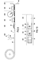
Un procédé de fabrication collectif d'une pluralité de cartes à puce selon un mode de réalisation particulier de l'invention est à présent décrit en référence aux
Une bobine 58 de feuilles en plastique est déroulée progressivement jusqu'à un premier poste de fraisage (ou de découpe) où des motifs 60 sont réalisés (E28) au moyen d'un dispositif de fraisage (ou de découpe) 59. Puis les feuilles comportant ces motifs sont transportées successivement aux différents postes opérationnels chargés de réaliser les étapes de fabrication successives E30 à E38.A
Les motifs 60 comprennent une cavité débouchante (ou évidement) 70 au fond desquelles sont formés des orifices traversants 72 (
Au cours d'une étape E30, un module 20 est inséré (au moyen d'un dispositif « pick and place ») dans la cavité 70 prévue à cet effet de sorte que chaque plot de contact présent sur la première face du substrat du module s'engage dans l'un des orifices traversant 72.During a step E30, a
Ainsi, la formation de la cavité 70 est effectuée avant la fixation du module 20.Thus, the formation of the
Une pression à chaud est ensuite appliquée (E32) au moyen d'une presse 64 sur la deuxième face du module comportant la puce 24.A hot pressure is then applied (E32) by means of a
Une couche comprenant une sous-couche plastique et une sous-couche d'adhésif activable par exemple par pression à chaud (comme représenté en
Cette couche d'adhésion est activée (E36) par la suite par lamination au moyen d'un dispositif 66.This adhesion layer is activated (E36) subsequently by lamination by means of a
Le module 20 est ainsi introduit dans la cavité 70 avant de procéder à une lamination.The
Une étape de découpe (« card punch ») E38 est ensuite réalisée afin de découper les cartes à puce selon le format souhaité.A card punching step E38 is then performed in order to cut the smart cards according to the desired format.
En résumé, conformément à l'invention, le module au sens de l'invention est fixé au corps de carte de sorte que la première face dudit module est montée en appui contre la face interne de la première couche (le cas échéant au fond d'une cavité réalisée à cet effet). Cette fixation est réalisée de sorte que chaque plot de contact s'engage dans un orifice traversant respectif de façon à être accessible par un dispositif externe depuis la première face du corps de carte. Un tel dispositif externe est par exemple un terminal de lecture de cartes bancaire. L'accès aux plots de contact se fait par exemple au moyen de broches de contact dont est muni le dispositif externe, ces broches étant configurées pour rentrer en contact avec la surface libre des plots de contact.In summary, according to the invention, the module in the sense of the invention is attached to the card body so that the first face of said module is mounted in abutment against the inner face of the first layer (where appropriate at the bottom of the card). a cavity made for this purpose). This fixation is carried out so that each contact pad engages in a respective through hole so as to be accessible by an external device from the first face of the card body. Such an external device is for example a bank card reading terminal. Access to the contact pads is done for example by means of contact pins which is provided with the external device, these pins being configured to come into contact with the free surface of the contact pads.
Le procédé de fabrication de l'invention permet avantageusement de contrôler avec précision la différence de hauteur pouvant exister entre la face externe de la première couche et la surface libre de chaque plot une fois le module en position sur la face interne de la première couche.The manufacturing method of the invention advantageously makes it possible to precisely control the difference in height that can exist between the external face of the first layer and the free surface of each stud once the module is in position on the internal face of the first layer.
L'invention permet ainsi d'améliorer le positionnement des plots de contact par rapport à la face supérieure de la carte à puce, ce positionnement étant critique pour permettre un accès dans de bonnes conditions d'un dispositif externe aux plots de contact de la carte. Le positionnement en hauteur des plots de contact n'est en effet plus dépendant des variations en épaisseur de la couche supérieure et/ou en positionnement de la couche inférieure ou encore de l'épaisseur d'une couche adhésive pouvant se trouver entre les couches supérieure et inférieure du corps de carte.The invention thus makes it possible to improve the positioning of the contact pads with respect to the upper face of the smart card, this positioning being critical to allow access under good conditions to a device external to the contact pads of the card. . The height positioning of the contact pads is in fact no longer dependent on variations in the thickness of the upper layer and / or in positioning of the lower layer or the thickness of an adhesive layer that can be between the upper layers and bottom of the card body.
Il est ainsi possible, pour un corps de carte donné, de sélectionner parmi plusieurs modules afin d'y monter le module le plus adapté selon les besoins (le module ayant en particulier l'épaisseur de plot de contact souhaitée), de sorte à obtenir la différence de hauteur souhaitée entre la face avant de la carte et les surfaces libres des plots de contact. Un même corps de carte pourra ainsi accueillir des modules ayant différentes tailles de plot de contact.It is thus possible, for a given card body, to select from several modules in order to mount the most appropriate module according to the needs (the module having in particular the desired contact pad thickness), so as to obtain the difference in height desired between the front face of the card and the free surfaces of the contact pads. The same card body can thus accommodate modules having different contact pad sizes.
Par ailleurs, contrairement au modèle antérieur de carte à puce représenté en
Un homme du métier comprendra que les modes de réalisation et variantes décrits ci-avant ne constituent que des exemples non limitatifs de mise en oeuvre de l'invention. En particulier, l'homme du métier pourra envisager une quelconque combinaison des variantes et modes de réalisation décrits ci-avant afin de répondre à un besoin bien particulier.Those skilled in the art will understand that the embodiments and variants described above are only non-limiting examples of implementation of the invention. In particular, those skilled in the art may consider any combination of variants and embodiments described above to meet a particular need.
Claims (15)
dans laquelle :
in which :
le procédé de fabrication comprenant :
the manufacturing process comprising:
la fixation (E8, E10) dudit module (20) comprenant l'insertion (E8) du module (20) dans ladite cavité (8) et le montage (E10) du module sur le fond de ladite cavité.A method according to claim 10 or 11, wherein the card body comprises a second layer (6) extending on the inner face (4b) of the first layer (4), the method comprising forming (E4) a cavity (8) in said second layer (6), a portion (8b) of the inner face (4b) of the first layer (4) forming the bottom of said cavity (8),
fixing (E8, E10) of said module (20) comprising insertion (E8) of the module (20) into said cavity (8) and mounting (E10) of the module on the bottom of said cavity.
le procédé comprenant en outre le dépôt d'un élément adhésif (27) entre la résine d'enrobage et la troisième couche de façon à fixer ensemble le module et la troisième couche.A method according to claim 14, wherein the closing step is carried out by fixing said third layer (35, 50) defined in (b), the chip (24) being covered with a coating resin (25) formed on the second face (22a) of the module (20) prior to insertion into said cavity (8),
the method further comprising depositing an adhesive member (27) between the coating resin and the third layer so as to secure the module and the third layer together.
Applications Claiming Priority (1)
| Application Number | Priority Date | Filing Date | Title |
|---|---|---|---|
| FR1357811A FR3009636B1 (en) | 2013-08-06 | 2013-08-06 | CHIP CARD AND METHOD FOR MANUFACTURING SUCH A CHIP CARD |
Publications (1)
| Publication Number | Publication Date |
|---|---|
| EP2835768A1 true EP2835768A1 (en) | 2015-02-11 |
Family
ID=49667328
Family Applications (1)
| Application Number | Title | Priority Date | Filing Date |
|---|---|---|---|
| EP14178864.6A Withdrawn EP2835768A1 (en) | 2013-08-06 | 2014-07-29 | Chip card and method for manufacturing such a chip card |
Country Status (2)
| Country | Link |
|---|---|
| EP (1) | EP2835768A1 (en) |
| FR (1) | FR3009636B1 (en) |
Citations (5)
| Publication number | Priority date | Publication date | Assignee | Title |
|---|---|---|---|---|
| US4222516A (en) | 1975-12-31 | 1980-09-16 | Compagnie Internationale Pour L'informatique Cii-Honeywell Bull | Standardized information card |
| EP0140230A1 (en) * | 1983-10-24 | 1985-05-08 | GAO Gesellschaft für Automation und Organisation mbH | Integrated circuit record carrier and process for making the same |
| DE4403513A1 (en) * | 1994-02-04 | 1995-08-10 | Giesecke & Devrient Gmbh | Chip card with an electronic module and method for producing such a chip card |
| US20090111522A1 (en) * | 2006-03-09 | 2009-04-30 | Javier Canis Robles | Smart Card and Method for Manufacturing Said Card |
| EP2461278A1 (en) * | 2010-12-06 | 2012-06-06 | Oberthur Technologies | Method for inserting a module in a chip card |
-
2013
- 2013-08-06 FR FR1357811A patent/FR3009636B1/en active Active
-
2014
- 2014-07-29 EP EP14178864.6A patent/EP2835768A1/en not_active Withdrawn
Patent Citations (5)
| Publication number | Priority date | Publication date | Assignee | Title |
|---|---|---|---|---|
| US4222516A (en) | 1975-12-31 | 1980-09-16 | Compagnie Internationale Pour L'informatique Cii-Honeywell Bull | Standardized information card |
| EP0140230A1 (en) * | 1983-10-24 | 1985-05-08 | GAO Gesellschaft für Automation und Organisation mbH | Integrated circuit record carrier and process for making the same |
| DE4403513A1 (en) * | 1994-02-04 | 1995-08-10 | Giesecke & Devrient Gmbh | Chip card with an electronic module and method for producing such a chip card |
| US20090111522A1 (en) * | 2006-03-09 | 2009-04-30 | Javier Canis Robles | Smart Card and Method for Manufacturing Said Card |
| EP2461278A1 (en) * | 2010-12-06 | 2012-06-06 | Oberthur Technologies | Method for inserting a module in a chip card |
Also Published As
| Publication number | Publication date |
|---|---|
| FR3009636B1 (en) | 2015-09-04 |
| FR3009636A1 (en) | 2015-02-13 |
Similar Documents
| Publication | Publication Date | Title |
|---|---|---|
| FR2660092A1 (en) | METHOD FOR MANUFACTURING INTEGRATED CIRCUIT BOARD | |
| FR2756955A1 (en) | METHOD FOR PRODUCING AN ELECTRONIC CIRCUIT FOR A CONTACTLESS MEMORY CARD | |
| WO2014041107A1 (en) | Cap for a chip device having a groove, device provided with said cap, assembly consisting of the device and a wire element, and manufacturing method thereof | |
| WO2014068240A1 (en) | Method for producing a smart card having a plurality of components and card obtained in this way | |
| EP2178032B1 (en) | Module, chip card and corresponding manufacturing method | |
| EP1559068B1 (en) | Electronic module comprising an element exposed on one surface and method for making same | |
| EP3408799B1 (en) | Method for manufacturing a smart card module and a smart card | |
| EP2323078B1 (en) | Contactless electronic device, method for manufacturing the device and contactless electronic tag | |
| EP1073996A1 (en) | Method for making chip cards | |
| EP2002384B1 (en) | Radiofrequency device | |
| EP2410472A1 (en) | Transponder insert and device including such an insert | |
| WO2001043066A1 (en) | Medium body comprising a security element | |
| EP3483790B1 (en) | Security device such as a smart card | |
| WO2003032241A1 (en) | Electronic module with protective bump | |
| EP2835768A1 (en) | Chip card and method for manufacturing such a chip card | |
| EP2933759A1 (en) | Method for manufacturing a device with an electrical/electronic circuit | |
| EP1190379B1 (en) | Method for producing contact chip cards with a low-cost dielectric | |
| FR2846446A1 (en) | CHIP CARD COMPRISING A CAPABLE COMPONENT AND A MANUFACTURING METHOD | |
| EP3020068B1 (en) | Electronic module and method for manufacturing same | |
| FR3009410A1 (en) | INTEGRATED COUPLING ELECTRONIC ENTITY BETWEEN A MICROCIRCUIT AND ANTENNA AND METHOD FOR MANUFACTURING THE SAME | |
| WO2003052526A1 (en) | Watch case base and method for making same | |
| FR3079645A1 (en) | ELECTRONIC DOCUMENT HAVING AN ELECTRICAL CONNECTION BETWEEN A CHIP PORT AND AN EXTERNAL ELECTRIC CONTACT BEACH ESTABLISHED VIA AN INLAY | |
| WO2013076410A1 (en) | Adapter for microcircuit card between a large format and a small format of lesser thickness | |
| WO2001015504A1 (en) | Method for making hybrid smart cards and smart cards obtained by said method | |
| WO2000077730A1 (en) | Electronic device comprising a chip fixed on a support and method for making same |
Legal Events
| Date | Code | Title | Description |
|---|---|---|---|
| PUAI | Public reference made under article 153(3) epc to a published international application that has entered the european phase |
Free format text: ORIGINAL CODE: 0009012 |
|
| 17P | Request for examination filed |
Effective date: 20140729 |
|
| AK | Designated contracting states |
Kind code of ref document: A1 Designated state(s): AL AT BE BG CH CY CZ DE DK EE ES FI FR GB GR HR HU IE IS IT LI LT LU LV MC MK MT NL NO PL PT RO RS SE SI SK SM TR |
|
| AX | Request for extension of the european patent |
Extension state: BA ME |
|
| R17P | Request for examination filed (corrected) |
Effective date: 20150730 |
|
| RBV | Designated contracting states (corrected) |
Designated state(s): AL AT BE BG CH CY CZ DE DK EE ES FI FR GB GR HR HU IE IS IT LI LT LU LV MC MK MT NL NO PL PT RO RS SE SI SK SM TR |
|
| 17Q | First examination report despatched |
Effective date: 20170620 |
|
| STAA | Information on the status of an ep patent application or granted ep patent |
Free format text: STATUS: THE APPLICATION IS DEEMED TO BE WITHDRAWN |
|
| 18D | Application deemed to be withdrawn |
Effective date: 20180103 |