EP2833550A1 - Composite substrate and elastic wave device - Google Patents
Composite substrate and elastic wave device Download PDFInfo
- Publication number
- EP2833550A1 EP2833550A1 EP20140774484 EP14774484A EP2833550A1 EP 2833550 A1 EP2833550 A1 EP 2833550A1 EP 20140774484 EP20140774484 EP 20140774484 EP 14774484 A EP14774484 A EP 14774484A EP 2833550 A1 EP2833550 A1 EP 2833550A1
- Authority
- EP
- European Patent Office
- Prior art keywords
- substrate
- coefficient
- thermal expansion
- composite substrate
- support substrate
- Prior art date
- Legal status (The legal status is an assumption and is not a legal conclusion. Google has not performed a legal analysis and makes no representation as to the accuracy of the status listed.)
- Granted
Links
Images



Classifications
-
- H—ELECTRICITY
- H10—SEMICONDUCTOR DEVICES; ELECTRIC SOLID-STATE DEVICES NOT OTHERWISE PROVIDED FOR
- H10N—ELECTRIC SOLID-STATE DEVICES NOT OTHERWISE PROVIDED FOR
- H10N30/00—Piezoelectric or electrostrictive devices
- H10N30/704—Piezoelectric or electrostrictive devices based on piezoelectric or electrostrictive films or coatings
-
- H—ELECTRICITY
- H03—ELECTRONIC CIRCUITRY
- H03H—IMPEDANCE NETWORKS, e.g. RESONANT CIRCUITS; RESONATORS
- H03H9/00—Networks comprising electromechanical or electro-acoustic elements; Electromechanical resonators
- H03H9/02—Details
- H03H9/02535—Details of surface acoustic wave devices
- H03H9/02818—Means for compensation or elimination of undesirable effects
- H03H9/02834—Means for compensation or elimination of undesirable effects of temperature influence
-
- H—ELECTRICITY
- H10—SEMICONDUCTOR DEVICES; ELECTRIC SOLID-STATE DEVICES NOT OTHERWISE PROVIDED FOR
- H10N—ELECTRIC SOLID-STATE DEVICES NOT OTHERWISE PROVIDED FOR
- H10N30/00—Piezoelectric or electrostrictive devices
- H10N30/01—Manufacture or treatment
- H10N30/07—Forming of piezoelectric or electrostrictive parts or bodies on an electrical element or another base
- H10N30/072—Forming of piezoelectric or electrostrictive parts or bodies on an electrical element or another base by laminating or bonding of piezoelectric or electrostrictive bodies
-
- H—ELECTRICITY
- H03—ELECTRONIC CIRCUITRY
- H03H—IMPEDANCE NETWORKS, e.g. RESONANT CIRCUITS; RESONATORS
- H03H9/00—Networks comprising electromechanical or electro-acoustic elements; Electromechanical resonators
- H03H9/02—Details
- H03H9/02535—Details of surface acoustic wave devices
- H03H9/02543—Characteristics of substrate, e.g. cutting angles
- H03H9/02574—Characteristics of substrate, e.g. cutting angles of combined substrates, multilayered substrates, piezoelectrical layers on not-piezoelectrical substrate
-
- Y—GENERAL TAGGING OF NEW TECHNOLOGICAL DEVELOPMENTS; GENERAL TAGGING OF CROSS-SECTIONAL TECHNOLOGIES SPANNING OVER SEVERAL SECTIONS OF THE IPC; TECHNICAL SUBJECTS COVERED BY FORMER USPC CROSS-REFERENCE ART COLLECTIONS [XRACs] AND DIGESTS
- Y10—TECHNICAL SUBJECTS COVERED BY FORMER USPC
- Y10T—TECHNICAL SUBJECTS COVERED BY FORMER US CLASSIFICATION
- Y10T428/00—Stock material or miscellaneous articles
- Y10T428/24—Structurally defined web or sheet [e.g., overall dimension, etc.]
- Y10T428/24942—Structurally defined web or sheet [e.g., overall dimension, etc.] including components having same physical characteristic in differing degree
Definitions
- the present invention relates to a composite substrate and an elastic wave device.
- a general process for forming elastic wave devices using the composite substrate as described above is performed as follows. First, elastic wave-device electrodes are formed on a surface of the piezoelectric substrate of the composite substrate. The surface of the piezoelectric substrate is partitioned so that many elastic wave devices are to be formed, and the elastic wave-device electrodes are formed using a photolithographic technique on positions of the respective elastic wave devices. Next, the composite substrate is diced along the partitions, so that many elastic wave devices are obtained.
- the piezoelectric substrate when heat is applied to the composite substrate in the process for forming elastic wave devices, a stress is generated by the difference in thermal expansion between the piezoelectric substrate and the support substrate. Hence, the composite substrate is considerably deformed, and the accuracy of the electrode width is degraded, so that the frequency characteristics may be degraded in some cases. In addition, depending on the cases, because of the stress generated at the interface between the piezoelectric substrate and the support substrate, the piezoelectric substrate may be peeled away from the support substrate or may be fractured in some cases.
- a composite substrate having a three-layer structure has been proposed in which a compensating layer having a coefficient of thermal expansion equivalent to that of a piezoelectric substrate is provided on a surface of a support substrate opposite to that in contact with the piezoelectric substrate (Patent Literature 1).
- Patent Literature 1 U.S. Patent No. 7408286
- Patent Literature 1 when the composite substrate disclosed in Patent Literature 1 is formed, a very complicated process is required, and it is difficult to realize this composite substrate.
- the present invention was made to overcome the problems as described above, and a primary object of the present invention is to provide a composite substrate having a relatively simple structure and preferable characteristics and an elastic wave device using the composite substrate described above.
- the present invention has the following configuration.
- a composite substrate of the present invention is formed by bonding a piezoelectric substrate and a support substrate having a coefficient of thermal expansion lower than that of the piezoelectric substrate, wherein the support substrate has a first surface bonded to the piezoelectric substrate and a second surface opposite to the first surface, and one specific characteristic value selected from the coefficient of thermal expansion and the Young's modulus is decreased along a thickness direction from the second surface to the first surface or to an intermediate position between the first surface and the second surface.
- intermediate position may be any position as long as being located between the first surface and the second surface, and for example, the intermediate position may be located at the center between the first surface and the second surface, at a position closer to the first surface than the center, or at a position closer to the second surface than the center.
- An elastic wave device of the present invention includes:
- the composite substrate of the present invention Since being capable of using a support substrate formed from a so-called functionally gradient material, the composite substrate of the present invention has a relatively simple structure.
- the specific characteristic value is the coefficient of thermal expansion
- the coefficient of thermal expansion is decreased along a thickness direction of the support substrate from the second surface to the intermediate position.
- the temperature coefficient of frequency can be made equivalent or superior to that of an elastic wave device formed using a related support substrate.
- the warpage of the substrate generated when the composite substrate is heated can also be reduced to be small.
- the specific characteristic value is the Young's modulus
- the Young's modulus is decreased along a thickness direction of the support substrate from the second surface to the intermediate position.
- a thermal stress at the bonding surface between the piezoelectric substrate and the support substrate is significantly reduced, and peeling between the two substrates can be significantly prevented.
- the elastic wave device of the present invention uses the composite substrate of the present invention described above.
- the specific characteristic value is the coefficient of thermal expansion
- the temperature coefficient of frequency can be made equivalent or superior to that of an elastic wave device formed using a relate support substrate.
- the specific characteristic value is the Young's modulus
- in an elastic wave device formed by using this composite substrate a stress at the bonding surface between the piezoelectric substrate and the support substrate is significantly reduced, and peeling between the two substrates can be significantly prevented.
- Fig. 1 is a perspective view of a composite substrate 10 of this embodiment
- Fig. 2 is a cross-sectional view taken along the line A-A in Fig. 1
- This composite substrate 10 includes a piezoelectric substrate 12 and a support substrate 14.
- the piezoelectric substrate 12 is a substrate capable of propagating an elastic wave.
- a material for this piezoelectric substrate 12 for example, there may be mentioned lithium tantalate (LT), lithium niobate (LN), a lithium niobate-lithium tantalate solid solution single crystal, quartz, lithium borate, zinc oxide, aluminum nitride, langasite (LGS), or langatate (LGT).
- LT or LN is preferable. The reason for this is that since having a high propagation rate of a surface acoustic wave and a high electromechanical coupling coefficient, LT and LN are each suitably used for a highfrequency or a wideband-frequency elastic wave device.
- the size of the piezoelectric substrate 12 is, for example, 50 to 150 mm in diameter and 0.2 to 50 ⁇ m in thickness.
- the coefficients of thermal expansion of representative materials used for the piezoelectric substrate 12 are shown in Table 1. [Table 1] Material Coefficient of thermal expansion (ppm/°C) Piezoelectric substrate Lithium tantalate 16.1 Lithium niobate 15.4 Quartz 13.7 Lithium borate 13
- the coefficient of thermal expansion of the support substrate 14 is changed along a thickness direction thereof, the coefficient of thermal expansion of the support substrate 14 is lower than that of the piezoelectric substrate 12, and the support substrate 14 is bonded directly to the rear surface of the piezoelectric substrate 12 or is bonded thereto with an organic adhesive layer interposed therebetween. Since the coefficient of thermal expansion of the support substrate 14 is set to be lower than that of the piezoelectric substrate 12, the change in size of the piezoelectric substrate 12 with the change in temperature is suppressed, and when the composite substrate 10 is used for an elastic wave device, the change in frequency characteristics with temperature can be suppressed.
- This support substrate 14 has a first surface 14a bonded to the piezoelectric substrate 12 and a second surface 14b opposite to the first surface 14a.
- the support substrate 14 is formed of a functionally gradient material in which the coefficient of thermal expansion is changed along its thickness direction.
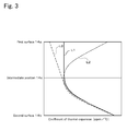
- Fig. 3 shows the relationship between the coefficient of thermal expansion of the support substrate 14 and the thickness direction thereof.
- the coefficient of thermal expansion of the support substrate 14 is decreased along the thickness direction from the second surface 14b to an intermediate position 14c located between the first surface 14a and the second surface 14b.
- the coefficient of thermal expansion of the pattern L1 is approximately constant from the intermediate position 14c to the first surface 14a; the coefficient of thermal expansion of the pattern L2 is increased along the thickness direction from the intermediate position 14c to the first surface 14a; and the coefficient of thermal expansion of the pattern L3 is decreased along the thickness direction from the intermediate position 14c to the first surface 14a.
- the coefficient of thermal expansion at the second surface 14b is higher than that at the intermediate position 14c.
- the coefficient of thermal expansion at the second surface 14b is preferably substantially approximately equivalent to that of the piezoelectric substrate 12.
- the coefficient of thermal expansion at the first surface 14a is also preferably substantially the same as that of the piezoelectric substrate 12.
- the "substantially the same” also includes the case in which the difference therebetween is within ⁇ 10%.
- the piezoelectric substrate 12 is formed of LT (having a coefficient of thermal expansion of 16.1 ppm/°C)
- the coefficient of thermal expansion at the second surface 14b is set to 15 to 17 ppm/°C.
- the size of the support substrate 14 is, for example, 50 to 150 mm in diameter and 100 to 500 ⁇ m in thickness.
- the intermediate position 14c of the support substrate 14 is not particularly limited as long as being located between the first surface 14a and the second surface 14b and, for example, may be located at the center between the first surface 14a and the second surface 14b, at a position closer to the first surface 14a than the center, or at a position closer to the second surface 14b than the center.
- the support substrate 14 is formed.
- the support substrate 14 may be formed in such a way that after at least three molded bodies (such as green sheets), material components of which are each adjusted so as to obtain desired characteristics, are laminated to each other to form a laminate, the laminate thus formed is fired.
- material components for example, various types of ceramic raw material powders may be mentioned. The representative examples thereof are shown in Table 2.
- the powders of the various piezoelectric materials shown in Table 1 each may also be used as a part of the support substrate and each may also be formed into a composite material in combination with at least one of the ceramics shown in Table 2.
- the support substrate 14 and the piezoelectric substrate 12 are bonded to each other.
- the first surface 14a of the support substrate 14 and the rear surface of the piezoelectric substrate 12 are bonded to each other.
- a bonding method either direct bonding or bonding with an organic adhesive layer interposed between the substrates may be used.
- bonding surfaces of the two substrates 12 and 14 are cleaned to remove dust and the like adhering to the bonding surfaces thereof.
- the bonding surfaces of the two substrates 12 and 14 are bonded to each other at ordinary temperature.
- an organic adhesive layer interposed between the substrates first, an organic adhesive is uniformly applied to at least one of the first surface 14a of the support substrate 14 and the rear surface of the piezoelectric substrate 12, and the organic adhesive is then solidified while the two substrates are overlapped with each other, so that the bonding is performed.
- the composite substrate 10 can be obtained.
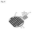
- Fig. 4 is a view illustrating a process for manufacturing elastic wave devices 30.
- elastic wave-device electrodes 31 are formed on a surface of the piezoelectric substrate 12 of the composite substrate 10.
- the surface of the piezoelectric substrate 12 is partitioned so that many elastic wave devices are to be formed, and the elastic wave-device electrodes 31 are formed at positions of respective elastic wave devices using a photolithographic technique.
- the electrodes 31 are each formed of IDT electrodes 32 and 34 and reflecting electrodes 36. Subsequently, dicing is performed along the partitions, so that many elastic wave devices 30 are obtained.
- the elastic wave device 30 is a surface acoustic wave device.
- the support substrate 14 formed of a so-called functionally gradient material can be used, and hence, a relatively simple structure is formed.
- the coefficient of thermal expansion of the support substrate 14 is decreased along the thickness direction of the support substrate 14 from the second surface 14b to the intermediate position 14c.
- the temperature coefficient of frequency is made equivalent or superior to that of an elastic wave device formed using a related support substrate.
- the warpage of the substrate generated when the composite substrate 10 is heated can also be reduced to be small.
- an effect of reducing the warpage becomes more significant in the case of using the pattern L2 (in which the coefficient of thermal expansion at the first surface 14a and the coefficient of thermal expansion at the second surface 14b are equal or approximately equal to that of the piezoelectric substrate 12, the coefficient of thermal expansion is decreased from the second surface 14b to the intermediate position 14c, and the coefficient of thermal expansion is increased from the intermediate position 14c to the first surface 14a).
- TCF temperature coefficient of frequency
- the patterns L1 to L3 showing the change in coefficient of thermal expansion along the thickness direction of the support substrate 14 are each illustrated as a smooth curve as shown in Fig. 3
- the patterns L1 to L3 each may be a step function pattern.
- the pattern L2 may be a pattern as shown by the solid line in Fig. 5 .
- the shape of the pattern L2 from the second surface 14b to the intermediate position 14c may have an S shape as shown by the two-dot chain line in Fig. 5 .
- the support substrate 14 is formed by firing a laminate including at least three molded bodies laminated to each other, as long as the coefficient of thermal expansion of one layer thereof is lower than that of the piezoelectric substrate 12, although the coefficient of thermal expansions of the other layers are preferably lower than that of the piezoelectric substrate 12, some of the other layers may have a higher coefficient of thermal expansion.
- a LiTaO 3 substrate having a thickness of 180 ⁇ m and a diameter of 100 mm was prepared.
- a support substrate there was prepared a substrate having a thickness of 200 ⁇ m and a diameter of 100 mm and formed of a functionally gradient material in which the coefficient of thermal expansion in a substrate thickness direction was changed as shown in Fig. 6 .
- This support substrate was formed so that the coefficients of thermal expansion at a first surface, an intermediate position, and a second surface were set to 3, 3, and 16 ppm/°C, respectively.
- the support substrate as described above was prepared as follows. First, three types of powdered materials, that is, silicon nitride, zirconia, and lithium tantalate, were prepared. Next, the weight ratio was adjusted so as to have a coefficient of thermal expansion shown in Fig. 6 , and five thin green sheets were formed. Subsequently, those green sheets were laminated together and were then integrally fired.
- the piezoelectric substrate and the support substrate were placed in a vacuum chamber in which the degree of vacuum was maintained on the order of 10 -6 Pa, and the rear surface of the piezoelectric substrate and the first surface of the support substrate were held so as to face each other.
- the rear surface of the piezoelectric substrate and the first surface of the support substrate were irradiated with Ar beams for 80 seconds to remove an inactive layer on each surface, so that the surfaces were activated.
- the two substrates were brought into contact with and bonded to each other by applying a load of 1,200 kgf, so that a laminated substrate was formed. After this laminated substrate was recovered from the vacuum chamber, the piezoelectric substrate was ground by a grinding machine to have a thickness of 30 ⁇ m.
- the laminated substrate thus ground was set in a lapping machine, and the piezoelectric substrate was polished using a diamond slurry to have a thickness of 21 ⁇ m. Furthermore, the surface of the piezoelectric substrate was polished by a CMP polishing machine to have a thickness of 20 ⁇ m, so that a work-affected layer was removed.
- a polishing agent colloidal silica was used as a polishing agent. As described above, a composite substrate of Example 1 was obtained.
- a silicon substrate having a coefficient of thermal expansion of 3 ppm/°C (constant value) in a substrate thickness direction was prepared, and a composite substrate of Comparative Example 1 was formed by a method similar to that of Example 1.
- Example 1 and Comparative Example 1 were placed on a hot plate so that the second surface of each support substrate faced upward, and heating was performed to 250°C.
- the composite substrate of Comparative Example 1 was remarkably warped, and the end portion of the substrate rose from the upper surface of the hot plate by approximately 8 mm.
- the composite substrate of Example 1 was only slightly warped, and the end portion of the substrate rose from the upper surface of the hot plate only by approximately 2 mm. As described above, it could be confirmed that by the composite substrate of Example 1, the deformation of the substrate caused by heating could be significantly suppressed.
- a one-port SAW resonator was formed on the surface of the composite substrate of each of Example 1 and Comparative Example 1 at a piezoelectric substrate side, and the temperature coefficient of frequency (TCF) was measured.
- TCF temperature coefficient of frequency
- a measurement temperature range was set to -30°C to 90°C.
- the TCF of the composite substrate of Comparative Example 1 was -20 ppm/°C and was improved to approximately a half of that of a LiTaO 3 single plate.
- the TCF of the composite substrate of Example 1 was -25 ppm/°C and was slightly inferior to that of Comparative Example 1, a practically sufficient temperature compensation effect was obtained. As described above, it was confirmed that the composite substrate of Example 1 also had a high effect of improving the temperature characteristics.
- a support substrate there was prepared a substrate having a thickness of 200 ⁇ m and a diameter of 100 mm and formed of a functionally gradient material in which the coefficient of thermal expansion in a substrate thickness direction was changed as shown in Fig. 7 .
- This support substrate was formed so that the coefficients of thermal expansion at a first surface, an intermediate position, and a second surface were set to 16, 3, and 16 ppm/°C, respectively.
- a piezoelectric substrate the same substrate as that of Example 1 was prepared. In addition, an adhesive was applied to respective bonding surfaces of the support substrate and the piezoelectric substrate to have a thickness of 0.3 ⁇ m.
- Example 2 a composite substrate was formed.
- the composite substrate was again placed in an oven at 180°C and then aged for 8 hours, so that a composite substrate of Example 2 was obtained.
- the warpage and TCF of the composite substrate of Example 2 were evaluated in a manner similar to that of Example 1. As a result, the warpage of the composite substrate was further reduced, and the rise of the substrate end from the upper surface of the hot plate caused by heating to 250°C was 1 mm or less. On the other hand, although the TCF was -27 ppm/°C, and the improvement effect was observed as compared to that of a LiTaO 3 single plate, the effect was slightly inferior to that of Example 1. In addition, according to calculation, a thermal stress generated at a bonding interface was approximately one fourth of that of Example 1. Hence, it is expected that the heat resistance be significantly improved. As described above, in the composite substrate of Example 2, although an appropriate effect of improving the TCF was obtained, the deformation of the substrate caused by heating was further significantly suppressed, and the thermal stress generated at the bonding interface could also be significantly reduced.
- a support substrate there was prepared a substrate having a thickness of 200 ⁇ m and a diameter of 100 mm and formed of a functionally gradient material in which the coefficient of thermal expansion in a substrate thickness direction was changed as shown in Fig. 8 .
- This support substrate was formed so that the Young's moduli at a first surface and a second surface were set to 160 and 20 GPa, respectively, and hence, the Young's modulus was decreased from the second surface to the first surface.
- the coefficient of thermal expansion in a substrate thickness direction of this support substrate was set to 3 ppm/°C (constant value).
- a composite substrate of Example 3 was formed by a method similar to that of Example 1.
- a substrate As a support substrate, a substrate was prepared which had a coefficient of thermal expansion of 3 ppm/°C (constant value) and a Young's modulus of 160 GPa (constant value) in a substrate thickness direction, and a composite substrate of Comparative Example 2 was formed by a method similar to that of Example 1.
- Example 3 When the thermal stress generated at the bonding interface of the composite substrate of each of Example 3 and Comparative Example 2 was calculated, the thermal stress of Example 3 was dramatically decreased to one third or less of that of Comparative Example 2. On the other hand, the warpage of the composite substrate of Example 3 was large, and the rise of the substrate end from the front surface of the hot plate caused by heating to 250°C was 10 mm. In addition, the TCF of Example 3 was -29 ppm/°C and was approximately the same as that of Comparative Example 3. As described above, although the effect of improving the warpage and TCF was not so much significant in the composite substrate of Example 3, the thermal stress generated at the bonding interface was dramatically reduced.
- the present invention may be applied to an elastic wave device, such as a SAW filter.
Landscapes
- Physics & Mathematics (AREA)
- Acoustics & Sound (AREA)
- Engineering & Computer Science (AREA)
- Manufacturing & Machinery (AREA)
- Surface Acoustic Wave Elements And Circuit Networks Thereof (AREA)
Abstract
Description
- The present invention relates to a composite substrate and an elastic wave device.
- In recent years, in order to improve frequency-temperature characteristics of an elastic wave device, a composite substrate formed by bonding a piezoelectric substrate onto a support substrate having a low coefficient of thermal expansion has been used. A general process for forming elastic wave devices using the composite substrate as described above is performed as follows. First, elastic wave-device electrodes are formed on a surface of the piezoelectric substrate of the composite substrate. The surface of the piezoelectric substrate is partitioned so that many elastic wave devices are to be formed, and the elastic wave-device electrodes are formed using a photolithographic technique on positions of the respective elastic wave devices. Next, the composite substrate is diced along the partitions, so that many elastic wave devices are obtained.
- However, when heat is applied to the composite substrate in the process for forming elastic wave devices, a stress is generated by the difference in thermal expansion between the piezoelectric substrate and the support substrate. Hence, the composite substrate is considerably deformed, and the accuracy of the electrode width is degraded, so that the frequency characteristics may be degraded in some cases. In addition, depending on the cases, because of the stress generated at the interface between the piezoelectric substrate and the support substrate, the piezoelectric substrate may be peeled away from the support substrate or may be fractured in some cases. As a method to overcome the problems as described above, a composite substrate having a three-layer structure has been proposed in which a compensating layer having a coefficient of thermal expansion equivalent to that of a piezoelectric substrate is provided on a surface of a support substrate opposite to that in contact with the piezoelectric substrate (Patent Literature 1).
- Patent Literature 1:
U.S. Patent No. 7408286 - However, when the composite substrate disclosed in Patent Literature 1 is formed, a very complicated process is required, and it is difficult to realize this composite substrate.
- The present invention was made to overcome the problems as described above, and a primary object of the present invention is to provide a composite substrate having a relatively simple structure and preferable characteristics and an elastic wave device using the composite substrate described above.
- In order to achieve the above primary object, the present invention has the following configuration.
- A composite substrate of the present invention is formed by bonding a piezoelectric substrate and a support substrate having a coefficient of thermal expansion lower than that of the piezoelectric substrate,
wherein the support substrate has a first surface bonded to the piezoelectric substrate and a second surface opposite to the first surface, and one specific characteristic value selected from the coefficient of thermal expansion and the Young's modulus is decreased along a thickness direction from the second surface to the first surface or to an intermediate position between the first surface and the second surface. - In addition, the "intermediate position" may be any position as long as being located between the first surface and the second surface, and for example, the intermediate position may be located at the center between the first surface and the second surface, at a position closer to the first surface than the center, or at a position closer to the second surface than the center.
- An elastic wave device of the present invention includes:
- the composite substrate described above, and
- an elastic wave-device electrode formed on a surface of the piezoelectric substrate of the composite substrate. Advantageous Effects of Invention
- Since being capable of using a support substrate formed from a so-called functionally gradient material, the composite substrate of the present invention has a relatively simple structure. In addition, for example, when the specific characteristic value is the coefficient of thermal expansion, the coefficient of thermal expansion is decreased along a thickness direction of the support substrate from the second surface to the intermediate position. Hence, in an elastic wave device formed using the composite substrate of the present invention, the temperature coefficient of frequency can be made equivalent or superior to that of an elastic wave device formed using a related support substrate. In addition, the warpage of the substrate generated when the composite substrate is heated can also be reduced to be small. On the other hand, when the specific characteristic value is the Young's modulus, the Young's modulus is decreased along a thickness direction of the support substrate from the second surface to the intermediate position. Hence, a thermal stress at the bonding surface between the piezoelectric substrate and the support substrate is significantly reduced, and peeling between the two substrates can be significantly prevented.
- The elastic wave device of the present invention uses the composite substrate of the present invention described above. Hence, when the specific characteristic value is the coefficient of thermal expansion, in an elastic wave device formed by using this composite substrate, the temperature coefficient of frequency can be made equivalent or superior to that of an elastic wave device formed using a relate support substrate. On the other hand, when the specific characteristic value is the Young's modulus, in an elastic wave device formed by using this composite substrate, a stress at the bonding surface between the piezoelectric substrate and the support substrate is significantly reduced, and peeling between the two substrates can be significantly prevented.
-
-
Fig. 1 is a perspective view of acomposite substrate 10. -
Fig. 2 is a cross-sectional view taken along the line A-A inFig. 1 . -
Fig. 3 is a graph showing the change in coefficient of thermal expansion along a thickness direction of asupport substrate 14. -
Fig. 4 is a view illustrating a process for manufacturingelastic wave devices 30. -
Fig. 5 is a graph showing the change in coefficient of thermal expansion along the thickness direction of thesupport substrate 14. -
Fig. 6 is a graph showing the change in coefficient of thermal expansion along a thickness direction of a support substrate used in Example 1. -
Fig. 7 is a graph showing the change in coefficient of thermal expansion along a thickness direction of a support substrate used in Example 2. -
Fig. 8 is a graph showing the change in Young's modulus along a thickness direction of a support substrate used in Example 3. - Next, an embodiment of the present invention will be described with reference to the drawings.
Fig. 1 is a perspective view of acomposite substrate 10 of this embodiment, andFig. 2 is a cross-sectional view taken along the line A-A inFig. 1 . Thiscomposite substrate 10 includes apiezoelectric substrate 12 and asupport substrate 14. - The
piezoelectric substrate 12 is a substrate capable of propagating an elastic wave. As a material for thispiezoelectric substrate 12, for example, there may be mentioned lithium tantalate (LT), lithium niobate (LN), a lithium niobate-lithium tantalate solid solution single crystal, quartz, lithium borate, zinc oxide, aluminum nitride, langasite (LGS), or langatate (LGT). Among those mentioned above, LT or LN is preferable. The reason for this is that since having a high propagation rate of a surface acoustic wave and a high electromechanical coupling coefficient, LT and LN are each suitably used for a highfrequency or a wideband-frequency elastic wave device. The size of thepiezoelectric substrate 12 is, for example, 50 to 150 mm in diameter and 0.2 to 50 µm in thickness. The coefficients of thermal expansion of representative materials used for thepiezoelectric substrate 12 are shown in Table 1.[Table 1] Material Coefficient of thermal expansion (ppm/°C) Piezoelectric substrate Lithium tantalate 16.1 Lithium niobate 15.4 Quartz 13.7 Lithium borate 13 - Although the coefficient of thermal expansion of the
support substrate 14 is changed along a thickness direction thereof, the coefficient of thermal expansion of thesupport substrate 14 is lower than that of thepiezoelectric substrate 12, and thesupport substrate 14 is bonded directly to the rear surface of thepiezoelectric substrate 12 or is bonded thereto with an organic adhesive layer interposed therebetween. Since the coefficient of thermal expansion of thesupport substrate 14 is set to be lower than that of thepiezoelectric substrate 12, the change in size of thepiezoelectric substrate 12 with the change in temperature is suppressed, and when thecomposite substrate 10 is used for an elastic wave device, the change in frequency characteristics with temperature can be suppressed. Thissupport substrate 14 has afirst surface 14a bonded to thepiezoelectric substrate 12 and asecond surface 14b opposite to thefirst surface 14a. Thesupport substrate 14 is formed of a functionally gradient material in which the coefficient of thermal expansion is changed along its thickness direction.Fig. 3 shows the relationship between the coefficient of thermal expansion of thesupport substrate 14 and the thickness direction thereof. In all three patterns L1 to L3, the coefficient of thermal expansion of thesupport substrate 14 is decreased along the thickness direction from thesecond surface 14b to anintermediate position 14c located between thefirst surface 14a and thesecond surface 14b. In addition, the coefficient of thermal expansion of the pattern L1 is approximately constant from theintermediate position 14c to thefirst surface 14a; the coefficient of thermal expansion of the pattern L2 is increased along the thickness direction from theintermediate position 14c to thefirst surface 14a; and the coefficient of thermal expansion of the pattern L3 is decreased along the thickness direction from theintermediate position 14c to thefirst surface 14a. In addition, in all the three patterns L1 to L3, the coefficient of thermal expansion at thesecond surface 14b is higher than that at theintermediate position 14c. In order to reduce the warpage of thecomposite substrate 10, the coefficient of thermal expansion at thesecond surface 14b is preferably substantially approximately equivalent to that of thepiezoelectric substrate 12. In the pattern L2, the coefficient of thermal expansion at thefirst surface 14a is also preferably substantially the same as that of thepiezoelectric substrate 12. In addition, besides the case in which the two coefficients are equal to each other, the "substantially the same" also includes the case in which the difference therebetween is within ±10%. For example, when thepiezoelectric substrate 12 is formed of LT (having a coefficient of thermal expansion of 16.1 ppm/°C), the coefficient of thermal expansion at thesecond surface 14b is set to 15 to 17 ppm/°C. The size of thesupport substrate 14 is, for example, 50 to 150 mm in diameter and 100 to 500 µm in thickness. - The
intermediate position 14c of thesupport substrate 14 is not particularly limited as long as being located between thefirst surface 14a and thesecond surface 14b and, for example, may be located at the center between thefirst surface 14a and thesecond surface 14b, at a position closer to thefirst surface 14a than the center, or at a position closer to thesecond surface 14b than the center. - Next, a method for manufacturing the
composite substrate 10 as described above will be described. First, thesupport substrate 14 is formed. Thesupport substrate 14 may be formed in such a way that after at least three molded bodies (such as green sheets), material components of which are each adjusted so as to obtain desired characteristics, are laminated to each other to form a laminate, the laminate thus formed is fired. In addition, as the material components, for example, various types of ceramic raw material powders may be mentioned. The representative examples thereof are shown in Table 2. The powders of the various piezoelectric materials shown in Table 1 each may also be used as a part of the support substrate and each may also be formed into a composite material in combination with at least one of the ceramics shown in Table 2. Subsequently, thesupport substrate 14 and thepiezoelectric substrate 12 are bonded to each other. In particular, thefirst surface 14a of thesupport substrate 14 and the rear surface of thepiezoelectric substrate 12 are bonded to each other. As a bonding method, either direct bonding or bonding with an organic adhesive layer interposed between the substrates may be used. In the case of the direct bonding, first, bonding surfaces of the twosubstrates substrates substrates first surface 14a of thesupport substrate 14 and the rear surface of thepiezoelectric substrate 12, and the organic adhesive is then solidified while the two substrates are overlapped with each other, so that the bonding is performed. As described above, thecomposite substrate 10 can be obtained.[Table 2] Material Formula, etc. Coefficient of thermal expansion (ppm/°C) Ceramics Silicon nitride Si3N4 3 Silicon carbide SiC 4 Aluminum nitride AlN 5 Alumina Al2O3 8 Zirconia ZrO 2 10 - Next, a method for forming an elastic wave device using the
composite substrate 10 as described above will be described with reference toFig. 4. Fig. 4 is a view illustrating a process for manufacturingelastic wave devices 30. First, elastic wave-device electrodes 31 are formed on a surface of thepiezoelectric substrate 12 of thecomposite substrate 10. The surface of thepiezoelectric substrate 12 is partitioned so that many elastic wave devices are to be formed, and the elastic wave-device electrodes 31 are formed at positions of respective elastic wave devices using a photolithographic technique. In addition, theelectrodes 31 are each formed ofIDT electrodes electrodes 36. Subsequently, dicing is performed along the partitions, so that manyelastic wave devices 30 are obtained. When a high frequency signal is applied to the input-side IDT electrode 32 of theelastic wave device 30 thus obtained, an electric field is generated between the electrodes, and a surface acoustic wave is excited and propagated on thepiezoelectric substrate 12. In addition, from the output-side IDT electrode 34 provided in a propagation direction, the surface acoustic wave thus propagated can be obtained as an electrical signal. That is, theelastic wave device 30 is a surface acoustic wave device. - According to the embodiment described above, the
support substrate 14 formed of a so-called functionally gradient material can be used, and hence, a relatively simple structure is formed. In addition, as shown by the patterns L1 to L3 shown inFig. 3 , the coefficient of thermal expansion of thesupport substrate 14 is decreased along the thickness direction of thesupport substrate 14 from thesecond surface 14b to theintermediate position 14c. Hence, in the elastic wave device formed by using thecomposite substrate 10, the temperature coefficient of frequency is made equivalent or superior to that of an elastic wave device formed using a related support substrate. In addition, the warpage of the substrate generated when thecomposite substrate 10 is heated can also be reduced to be small. - Compared to the case of using the patterns L1 and L3, an effect of reducing the warpage becomes more significant in the case of using the pattern L2 (in which the coefficient of thermal expansion at the
first surface 14a and the coefficient of thermal expansion at thesecond surface 14b are equal or approximately equal to that of thepiezoelectric substrate 12, the coefficient of thermal expansion is decreased from thesecond surface 14b to theintermediate position 14c, and the coefficient of thermal expansion is increased from theintermediate position 14c to thefirst surface 14a). On the other hand, since an effect of improving the temperature coefficient of frequency (TCF) is high when the coefficient of thermal expansion is low at thefirst surface 14a, the effect described above is significant in the case of each of the patterns L1 and L3 as compared to that in the case of the pattern L2. - The present invention is not limited to the above-described embodiment. It is clear that the present invention can be implemented in a variety of embodiments without departing from the technical scope thereof.
- For example, in the embodiment described above, although the patterns L1 to L3 showing the change in coefficient of thermal expansion along the thickness direction of the
support substrate 14 are each illustrated as a smooth curve as shown inFig. 3 , the patterns L1 to L3 each may be a step function pattern. For example, the pattern L2 may be a pattern as shown by the solid line inFig. 5 . - In addition, as long as the coefficient of thermal expansion along the thickness direction of the
support substrate 14 is decreased from thesecond surface 14b to theintermediate position 14c, for example, the shape of the pattern L2 from thesecond surface 14b to theintermediate position 14c may have an S shape as shown by the two-dot chain line inFig. 5 . Furthermore, when thesupport substrate 14 is formed by firing a laminate including at least three molded bodies laminated to each other, as long as the coefficient of thermal expansion of one layer thereof is lower than that of thepiezoelectric substrate 12, although the coefficient of thermal expansions of the other layers are preferably lower than that of thepiezoelectric substrate 12, some of the other layers may have a higher coefficient of thermal expansion. - As a piezoelectric substrate, a LiTaO3 substrate having a thickness of 180 µm and a diameter of 100 mm was prepared. In addition, as a support substrate, there was prepared a substrate having a thickness of 200 µm and a diameter of 100 mm and formed of a functionally gradient material in which the coefficient of thermal expansion in a substrate thickness direction was changed as shown in
Fig. 6 . This support substrate was formed so that the coefficients of thermal expansion at a first surface, an intermediate position, and a second surface were set to 3, 3, and 16 ppm/°C, respectively. The support substrate as described above was prepared as follows. First, three types of powdered materials, that is, silicon nitride, zirconia, and lithium tantalate, were prepared. Next, the weight ratio was adjusted so as to have a coefficient of thermal expansion shown inFig. 6 , and five thin green sheets were formed. Subsequently, those green sheets were laminated together and were then integrally fired. - Next, the piezoelectric substrate and the support substrate were placed in a vacuum chamber in which the degree of vacuum was maintained on the order of 10-6 Pa, and the rear surface of the piezoelectric substrate and the first surface of the support substrate were held so as to face each other. The rear surface of the piezoelectric substrate and the first surface of the support substrate were irradiated with Ar beams for 80 seconds to remove an inactive layer on each surface, so that the surfaces were activated. Next, the two substrates were brought into contact with and bonded to each other by applying a load of 1,200 kgf, so that a laminated substrate was formed. After this laminated substrate was recovered from the vacuum chamber, the piezoelectric substrate was ground by a grinding machine to have a thickness of 30 µm. Next, the laminated substrate thus ground was set in a lapping machine, and the piezoelectric substrate was polished using a diamond slurry to have a thickness of 21 µm. Furthermore, the surface of the piezoelectric substrate was polished by a CMP polishing machine to have a thickness of 20 µm, so that a work-affected layer was removed. In this step, as a polishing agent, colloidal silica was used. As described above, a composite substrate of Example 1 was obtained.
- As a support substrate, a silicon substrate having a coefficient of thermal expansion of 3 ppm/°C (constant value) in a substrate thickness direction was prepared, and a composite substrate of Comparative Example 1 was formed by a method similar to that of Example 1.
- The composite substrates of Example 1 and Comparative Example 1 were placed on a hot plate so that the second surface of each support substrate faced upward, and heating was performed to 250°C. As a result, the composite substrate of Comparative Example 1 was remarkably warped, and the end portion of the substrate rose from the upper surface of the hot plate by approximately 8 mm. On the other hand, the composite substrate of Example 1 was only slightly warped, and the end portion of the substrate rose from the upper surface of the hot plate only by approximately 2 mm. As described above, it could be confirmed that by the composite substrate of Example 1, the deformation of the substrate caused by heating could be significantly suppressed.
- Next, a one-port SAW resonator was formed on the surface of the composite substrate of each of Example 1 and Comparative Example 1 at a piezoelectric substrate side, and the temperature coefficient of frequency (TCF) was measured. A measurement temperature range was set to -30°C to 90°C.
The TCF of the composite substrate of Comparative Example 1 was -20 ppm/°C and was improved to approximately a half of that of a LiTaO3 single plate. On the other hand, although the TCF of the composite substrate of Example 1 was -25 ppm/°C and was slightly inferior to that of Comparative Example 1, a practically sufficient temperature compensation effect was obtained. As described above, it was confirmed that the composite substrate of Example 1 also had a high effect of improving the temperature characteristics. - As a support substrate, there was prepared a substrate having a thickness of 200 µm and a diameter of 100 mm and formed of a functionally gradient material in which the coefficient of thermal expansion in a substrate thickness direction was changed as shown in
Fig. 7 . This support substrate was formed so that the coefficients of thermal expansion at a first surface, an intermediate position, and a second surface were set to 16, 3, and 16 ppm/°C, respectively. As a piezoelectric substrate, the same substrate as that of Example 1 was prepared. In addition, an adhesive was applied to respective bonding surfaces of the support substrate and the piezoelectric substrate to have a thickness of 0.3 µm. Subsequently, the two substrates were adhered to each other and then aged in an oven at 100°C for 4 hours, so that the two substrates were pre-bonded to each other. Next, by a polishing method similar to that of Example 1, a composite substrate was formed. The composite substrate was again placed in an oven at 180°C and then aged for 8 hours, so that a composite substrate of Example 2 was obtained. - The warpage and TCF of the composite substrate of Example 2 were evaluated in a manner similar to that of Example 1. As a result, the warpage of the composite substrate was further reduced, and the rise of the substrate end from the upper surface of the hot plate caused by heating to 250°C was 1 mm or less. On the other hand, although the TCF was -27 ppm/°C, and the improvement effect was observed as compared to that of a LiTaO3 single plate, the effect was slightly inferior to that of Example 1. In addition, according to calculation, a thermal stress generated at a bonding interface was approximately one fourth of that of Example 1. Hence, it is expected that the heat resistance be significantly improved. As described above, in the composite substrate of Example 2, although an appropriate effect of improving the TCF was obtained, the deformation of the substrate caused by heating was further significantly suppressed, and the thermal stress generated at the bonding interface could also be significantly reduced.
- As a support substrate, there was prepared a substrate having a thickness of 200 µm and a diameter of 100 mm and formed of a functionally gradient material in which the coefficient of thermal expansion in a substrate thickness direction was changed as shown in
Fig. 8 . This support substrate was formed so that the Young's moduli at a first surface and a second surface were set to 160 and 20 GPa, respectively, and hence, the Young's modulus was decreased from the second surface to the first surface. In addition, the coefficient of thermal expansion in a substrate thickness direction of this support substrate was set to 3 ppm/°C (constant value). In addition, by using this support substrate, a composite substrate of Example 3 was formed by a method similar to that of Example 1. - As a support substrate, a substrate was prepared which had a coefficient of thermal expansion of 3 ppm/°C (constant value) and a Young's modulus of 160 GPa (constant value) in a substrate thickness direction, and a composite substrate of Comparative Example 2 was formed by a method similar to that of Example 1.
- When the thermal stress generated at the bonding interface of the composite substrate of each of Example 3 and Comparative Example 2 was calculated, the thermal stress of Example 3 was dramatically decreased to one third or less of that of Comparative Example 2. On the other hand, the warpage of the composite substrate of Example 3 was large, and the rise of the substrate end from the front surface of the hot plate caused by heating to 250°C was 10 mm. In addition, the TCF of Example 3 was -29 ppm/°C and was approximately the same as that of Comparative Example 3. As described above, although the effect of improving the warpage and TCF was not so much significant in the composite substrate of Example 3, the thermal stress generated at the bonding interface was dramatically reduced.
- The present application claims priority from Japanese Patent Application No.
2013-66319 filed on March 27, 2013 - The present invention may be applied to an elastic wave device, such as a SAW filter.
- 10 composite substrate, 12 piezoelectric substrate, 14 support substrate, 14a first surface, 14b second surface, 14c intermediate position, 30 elastic wave device (surface acoustic wave device), 31 electrode, 32, 34 IDT electrode, 36 reflecting electrode, L1 to L3 pattern
Claims (7)
- A composite substrate formed by bonding a piezoelectric substrate and a support substrate having a coefficient of thermal expansion lower than that of the piezoelectric substrate,
wherein the support substrate has a first surface bonded to the piezoelectric substrate and a second surface opposite to the first surface, and one specific characteristic value selected from the coefficient of thermal expansion and the Young's modulus is decreased along a thickness direction from the second surface to the first surface or to an intermediate position between the first surface and the second surface. - The composite substrate according to Claim 1,
wherein the specific characteristic value is increased along a thickness direction from the intermediate position to the first surface. - The composite substrate according to Claim 2,
wherein the specific characteristic value is the coefficient of thermal expansion, and the coefficients of thermal expansion at the first surface and the second surface are each substantially the same as that of the piezoelectric substrate. - The composite substrate according to Claim 1,
wherein the specific characteristic value is approximately constant along a thickness direction from the intermediate position to the first surface. - The composite substrate according to Claim 1,
wherein the specific characteristic value is decreased along a thickness direction from the intermediate position to the first surface. - The composite substrate according to any one of Claims 1 to 5,
wherein the support substrate is formed by firing a laminate including at least three layers having different compositions. - An elastic wave device comprising:the composite substrate according to any one of Claims 1 to 6, andan elastic wave-device electrode formed on a surface of the piezoelectric substrate of the composite substrate.
Applications Claiming Priority (2)
| Application Number | Priority Date | Filing Date | Title |
|---|---|---|---|
| JP2013066319 | 2013-03-27 | ||
| PCT/JP2014/055421 WO2014156507A1 (en) | 2013-03-27 | 2014-03-04 | Composite substrate and elastic wave device |
Publications (3)
| Publication Number | Publication Date |
|---|---|
| EP2833550A1 true EP2833550A1 (en) | 2015-02-04 |
| EP2833550A4 EP2833550A4 (en) | 2015-05-27 |
| EP2833550B1 EP2833550B1 (en) | 2017-05-10 |
Family
ID=51623497
Family Applications (1)
| Application Number | Title | Priority Date | Filing Date |
|---|---|---|---|
| EP14774484.1A Active EP2833550B1 (en) | 2013-03-27 | 2014-03-04 | Composite substrate and elastic wave device |
Country Status (6)
| Country | Link |
|---|---|
| US (1) | US9159901B2 (en) |
| EP (1) | EP2833550B1 (en) |
| JP (1) | JP5615472B1 (en) |
| KR (1) | KR101514193B1 (en) |
| CN (1) | CN104272592B (en) |
| WO (1) | WO2014156507A1 (en) |
Families Citing this family (14)
| Publication number | Priority date | Publication date | Assignee | Title |
|---|---|---|---|---|
| USD809804S1 (en) * | 2014-12-17 | 2018-02-13 | Ngk Insulators, Ltd. | Composite substrate for acoustic wave device |
| TWD174921S (en) | 2014-12-17 | 2016-04-11 | 日本碍子股份有限公司 | Portion of composite substrates |
| KR101959455B1 (en) | 2015-03-16 | 2019-03-18 | 가부시키가이샤 무라타 세이사쿠쇼 | Surface acoustic wave device |
| CN108028312B (en) * | 2015-09-15 | 2021-03-26 | 日本碍子株式会社 | Manufacturing method of composite substrate |
| FR3042649B1 (en) * | 2015-10-20 | 2019-06-21 | Soitec | METHOD FOR MANUFACTURING A HYBRID STRUCTURE |
| JP6590843B2 (en) * | 2017-02-02 | 2019-10-16 | 太陽誘電株式会社 | Elastic wave device |
| US11082027B2 (en) | 2017-02-02 | 2021-08-03 | Taiyo Yuden Co., Ltd. | Acoustic wave device |
| JP7224094B2 (en) | 2017-06-26 | 2023-02-17 | 太陽誘電株式会社 | Acoustic wave resonators, filters and multiplexers |
| USD966276S1 (en) | 2019-07-29 | 2022-10-11 | Samsung Display Co., Ltd. | Display module for wearable device |
| USD940131S1 (en) * | 2019-07-29 | 2022-01-04 | Samsung Display Co., Ltd. | Display panel |
| USD958094S1 (en) | 2019-07-29 | 2022-07-19 | Samsung Display Co., Ltd. | Display panel |
| CN110994097B (en) * | 2019-12-24 | 2021-12-07 | 无锡市好达电子股份有限公司 | High-frequency large-bandwidth thin-film bulk wave filter structure and preparation method thereof |
| KR102539925B1 (en) * | 2021-03-10 | 2023-06-02 | 엔지케이 인슐레이터 엘티디 | zygote |
| JP2022184454A (en) * | 2021-06-01 | 2022-12-13 | 三安ジャパンテクノロジー株式会社 | Laminate and method for manufacturing acoustic wave device |
Family Cites Families (27)
| Publication number | Priority date | Publication date | Assignee | Title |
|---|---|---|---|---|
| US3943389A (en) * | 1974-07-02 | 1976-03-09 | Motorola, Inc. | Temperature stabilization of surface acoustic wave substrates |
| JP3190702B2 (en) * | 1990-10-08 | 2001-07-23 | 株式会社東芝 | Method for manufacturing semiconductor device |
| JP2924177B2 (en) * | 1990-11-30 | 1999-07-26 | 株式会社村田製作所 | Functionally graded circuit board |
| JP3106365B2 (en) * | 1991-01-11 | 2000-11-06 | 株式会社村田製作所 | Functionally graded piezoelectric |
| JPH0520418U (en) * | 1991-08-24 | 1993-03-12 | 株式会社村田製作所 | Piezoelectric part exterior structure |
| US5446330A (en) * | 1993-03-15 | 1995-08-29 | Matsushita Electric Industrial Co., Ltd. | Surface acoustic wave device having a lamination structure |
| JPH06343274A (en) * | 1993-05-31 | 1994-12-13 | 晃 ▲徳▼島 | Ultrasonic motor |
| US6124635A (en) | 1997-03-21 | 2000-09-26 | Honda Giken Kogyo Kabushiki Kaisha | Functionally gradient integrated metal-ceramic member and semiconductor circuit substrate application thereof |
| JPH10270613A (en) * | 1997-03-21 | 1998-10-09 | Honda Motor Co Ltd | Semiconductor circuit board using functionally graded material |
| JP3880150B2 (en) * | 1997-06-02 | 2007-02-14 | 松下電器産業株式会社 | Surface acoustic wave device |
| US6426583B1 (en) * | 1999-06-14 | 2002-07-30 | Matsushita Electric Industrial Co., Ltd. | Surface acoustic wave element, method for producing the same and surface acoustic wave device using the same |
| JP3535470B2 (en) | 2001-03-30 | 2004-06-07 | 岐阜県 | Manufacturing method of functionally graded material |
| US7105980B2 (en) * | 2002-07-03 | 2006-09-12 | Sawtek, Inc. | Saw filter device and method employing normal temperature bonding for producing desirable filter production and performance characteristics |
| JP2004186868A (en) * | 2002-12-02 | 2004-07-02 | Fujitsu Media Device Kk | Surface acoustic wave element, transmission filter and reception filter having the same, and duplexer having the same |
| JP2007157971A (en) * | 2005-12-05 | 2007-06-21 | Nissan Motor Co Ltd | Thermal stress relaxation device |
| US7569976B2 (en) * | 2006-07-27 | 2009-08-04 | Koike Co., Ltd. | Piezo-electric substrate and manufacturing method of the same |
| US7408286B1 (en) | 2007-01-17 | 2008-08-05 | Rf Micro Devices, Inc. | Piezoelectric substrate for a saw device |
| JP2008301066A (en) * | 2007-05-30 | 2008-12-11 | Yamajiyu Ceramics:Kk | Lithium tantalate (lt) or lithium niobate (ln) single crystal compound substrate |
| JP2008306134A (en) * | 2007-06-11 | 2008-12-18 | Toyota Motor Corp | Semiconductor module |
| JP5180889B2 (en) * | 2009-03-25 | 2013-04-10 | 日本碍子株式会社 | Composite substrate, elastic wave device using the same, and method of manufacturing composite substrate |
| JP2011067915A (en) * | 2009-09-28 | 2011-04-07 | Sumitomo Electric Ind Ltd | Composite material, method for manufacturing composite material, and joint product using composite material |
| KR101661361B1 (en) * | 2010-01-14 | 2016-09-29 | 엔지케이 인슐레이터 엘티디 | Composite substrate, and elastic surface wave filter and resonator using the same |
| JP2012065304A (en) * | 2010-08-16 | 2012-03-29 | Seiko Epson Corp | Piezoelectric vibration device, method of manufacturing the same, and method of adjusting resonant frequency |
| JP5695394B2 (en) * | 2010-11-17 | 2015-04-01 | 日本碍子株式会社 | Composite substrate manufacturing method |
| US20130328451A1 (en) * | 2011-04-21 | 2013-12-12 | Panasonic Corporation | Dielectric element base material, method for producing same, and piezoelectric element using said dielectric element base material |
| WO2013141168A1 (en) * | 2012-03-23 | 2013-09-26 | 株式会社村田製作所 | Elastic wave device and manufacturing method for same |
| CN104396142B (en) * | 2012-07-12 | 2018-01-05 | 日本碍子株式会社 | Composite substrate, piezoelectric device and method for manufacturing composite substrate |
-
2014
- 2014-03-04 WO PCT/JP2014/055421 patent/WO2014156507A1/en not_active Ceased
- 2014-03-04 EP EP14774484.1A patent/EP2833550B1/en active Active
- 2014-03-04 JP JP2014531445A patent/JP5615472B1/en active Active
- 2014-03-04 CN CN201480001085.3A patent/CN104272592B/en active Active
- 2014-03-04 KR KR1020147030588A patent/KR101514193B1/en active Active
- 2014-10-23 US US14/521,854 patent/US9159901B2/en active Active
Also Published As
| Publication number | Publication date |
|---|---|
| EP2833550A4 (en) | 2015-05-27 |
| US9159901B2 (en) | 2015-10-13 |
| KR20140140634A (en) | 2014-12-09 |
| EP2833550B1 (en) | 2017-05-10 |
| CN104272592B (en) | 2016-12-07 |
| JPWO2014156507A1 (en) | 2017-02-16 |
| CN104272592A (en) | 2015-01-07 |
| US20150042207A1 (en) | 2015-02-12 |
| WO2014156507A1 (en) | 2014-10-02 |
| KR101514193B1 (en) | 2015-04-21 |
| JP5615472B1 (en) | 2014-10-29 |
Similar Documents
| Publication | Publication Date | Title |
|---|---|---|
| EP2833550B1 (en) | Composite substrate and elastic wave device | |
| KR102094026B1 (en) | Composite substrate, elastic wave device and method for manufacturing elastic wave device | |
| KR101972728B1 (en) | Bonded body and acoustic wave element | |
| KR101636220B1 (en) | Composite substrate, piezoelectric device and method of manufacturing composite substrate | |
| US20110041987A1 (en) | Method for manufacturing composite substrate | |
| KR101661361B1 (en) | Composite substrate, and elastic surface wave filter and resonator using the same | |
| CN203014754U (en) | Composite substrate | |
| JP3187231U (en) | Composite board | |
| KR102222096B1 (en) | Acoustic wave element and its manufacturing method | |
| US7911111B2 (en) | Surface acoustic wave devices | |
| JP2005229455A (en) | Composite piezoelectric substrate | |
| JP2009278610A (en) | Surface acoustic wave devices | |
| JP2007134889A (en) | Composite piezoelectric substrate | |
| JP2007214902A (en) | Surface acoustic wave device | |
| US20100269319A1 (en) | Method for manufacturing surface acoustic wave device | |
| KR102539925B1 (en) | zygote | |
| JP2006304206A (en) | Surface acoustic wave device, composite piezoelectric chip, and manufacturing method thereof | |
| WO2010103713A1 (en) | Surface acoustic wave element | |
| JP2011019043A (en) | Composite substrate and method for manufacturing composite substrate | |
| JP2011040999A (en) | Method for manufacturing surface acoustic wave device | |
| JP2014229943A (en) | Piezoelectric substrate, and elastic surface-wave device | |
| JP2015005931A (en) | Piezoelectric substrate, and elastic surface-wave device |
Legal Events
| Date | Code | Title | Description |
|---|---|---|---|
| PUAI | Public reference made under article 153(3) epc to a published international application that has entered the european phase |
Free format text: ORIGINAL CODE: 0009012 |
|
| 17P | Request for examination filed |
Effective date: 20141030 |
|
| AK | Designated contracting states |
Kind code of ref document: A1 Designated state(s): AL AT BE BG CH CY CZ DE DK EE ES FI FR GB GR HR HU IE IS IT LI LT LU LV MC MK MT NL NO PL PT RO RS SE SI SK SM TR |
|
| AX | Request for extension of the european patent |
Extension state: BA ME |
|
| REG | Reference to a national code |
Ref country code: DE Ref legal event code: R079 Ref document number: 602014009782 Country of ref document: DE Free format text: PREVIOUS MAIN CLASS: H03H0009250000 Ipc: H03H0009020000 |
|
| RA4 | Supplementary search report drawn up and despatched (corrected) |
Effective date: 20150424 |
|
| RIC1 | Information provided on ipc code assigned before grant |
Ipc: H03H 9/02 20060101AFI20150420BHEP |
|
| 17Q | First examination report despatched |
Effective date: 20160322 |
|
| DAX | Request for extension of the european patent (deleted) | ||
| GRAP | Despatch of communication of intention to grant a patent |
Free format text: ORIGINAL CODE: EPIDOSNIGR1 |
|
| INTG | Intention to grant announced |
Effective date: 20161028 |
|
| GRAS | Grant fee paid |
Free format text: ORIGINAL CODE: EPIDOSNIGR3 |
|
| GRAA | (expected) grant |
Free format text: ORIGINAL CODE: 0009210 |
|
| AK | Designated contracting states |
Kind code of ref document: B1 Designated state(s): AL AT BE BG CH CY CZ DE DK EE ES FI FR GB GR HR HU IE IS IT LI LT LU LV MC MK MT NL NO PL PT RO RS SE SI SK SM TR |
|
| REG | Reference to a national code |
Ref country code: GB Ref legal event code: FG4D |
|
| REG | Reference to a national code |
Ref country code: AT Ref legal event code: REF Ref document number: 893295 Country of ref document: AT Kind code of ref document: T Effective date: 20170515 Ref country code: CH Ref legal event code: EP |
|
| REG | Reference to a national code |
Ref country code: IE Ref legal event code: FG4D |
|
| REG | Reference to a national code |
Ref country code: DE Ref legal event code: R096 Ref document number: 602014009782 Country of ref document: DE |
|
| REG | Reference to a national code |
Ref country code: NL Ref legal event code: MP Effective date: 20170510 |
|
| REG | Reference to a national code |
Ref country code: LT Ref legal event code: MG4D |
|
| REG | Reference to a national code |
Ref country code: AT Ref legal event code: MK05 Ref document number: 893295 Country of ref document: AT Kind code of ref document: T Effective date: 20170510 |
|
| PG25 | Lapsed in a contracting state [announced via postgrant information from national office to epo] |
Ref country code: LT Free format text: LAPSE BECAUSE OF FAILURE TO SUBMIT A TRANSLATION OF THE DESCRIPTION OR TO PAY THE FEE WITHIN THE PRESCRIBED TIME-LIMIT Effective date: 20170510 Ref country code: NO Free format text: LAPSE BECAUSE OF FAILURE TO SUBMIT A TRANSLATION OF THE DESCRIPTION OR TO PAY THE FEE WITHIN THE PRESCRIBED TIME-LIMIT Effective date: 20170810 Ref country code: AT Free format text: LAPSE BECAUSE OF FAILURE TO SUBMIT A TRANSLATION OF THE DESCRIPTION OR TO PAY THE FEE WITHIN THE PRESCRIBED TIME-LIMIT Effective date: 20170510 Ref country code: ES Free format text: LAPSE BECAUSE OF FAILURE TO SUBMIT A TRANSLATION OF THE DESCRIPTION OR TO PAY THE FEE WITHIN THE PRESCRIBED TIME-LIMIT Effective date: 20170510 Ref country code: FI Free format text: LAPSE BECAUSE OF FAILURE TO SUBMIT A TRANSLATION OF THE DESCRIPTION OR TO PAY THE FEE WITHIN THE PRESCRIBED TIME-LIMIT Effective date: 20170510 Ref country code: HR Free format text: LAPSE BECAUSE OF FAILURE TO SUBMIT A TRANSLATION OF THE DESCRIPTION OR TO PAY THE FEE WITHIN THE PRESCRIBED TIME-LIMIT Effective date: 20170510 Ref country code: GR Free format text: LAPSE BECAUSE OF FAILURE TO SUBMIT A TRANSLATION OF THE DESCRIPTION OR TO PAY THE FEE WITHIN THE PRESCRIBED TIME-LIMIT Effective date: 20170811 |
|
| PG25 | Lapsed in a contracting state [announced via postgrant information from national office to epo] |
Ref country code: LV Free format text: LAPSE BECAUSE OF FAILURE TO SUBMIT A TRANSLATION OF THE DESCRIPTION OR TO PAY THE FEE WITHIN THE PRESCRIBED TIME-LIMIT Effective date: 20170510 Ref country code: RS Free format text: LAPSE BECAUSE OF FAILURE TO SUBMIT A TRANSLATION OF THE DESCRIPTION OR TO PAY THE FEE WITHIN THE PRESCRIBED TIME-LIMIT Effective date: 20170510 Ref country code: NL Free format text: LAPSE BECAUSE OF FAILURE TO SUBMIT A TRANSLATION OF THE DESCRIPTION OR TO PAY THE FEE WITHIN THE PRESCRIBED TIME-LIMIT Effective date: 20170510 Ref country code: PL Free format text: LAPSE BECAUSE OF FAILURE TO SUBMIT A TRANSLATION OF THE DESCRIPTION OR TO PAY THE FEE WITHIN THE PRESCRIBED TIME-LIMIT Effective date: 20170510 Ref country code: IS Free format text: LAPSE BECAUSE OF FAILURE TO SUBMIT A TRANSLATION OF THE DESCRIPTION OR TO PAY THE FEE WITHIN THE PRESCRIBED TIME-LIMIT Effective date: 20170910 Ref country code: SE Free format text: LAPSE BECAUSE OF FAILURE TO SUBMIT A TRANSLATION OF THE DESCRIPTION OR TO PAY THE FEE WITHIN THE PRESCRIBED TIME-LIMIT Effective date: 20170510 Ref country code: BG Free format text: LAPSE BECAUSE OF FAILURE TO SUBMIT A TRANSLATION OF THE DESCRIPTION OR TO PAY THE FEE WITHIN THE PRESCRIBED TIME-LIMIT Effective date: 20170810 |
|
| PG25 | Lapsed in a contracting state [announced via postgrant information from national office to epo] |
Ref country code: EE Free format text: LAPSE BECAUSE OF FAILURE TO SUBMIT A TRANSLATION OF THE DESCRIPTION OR TO PAY THE FEE WITHIN THE PRESCRIBED TIME-LIMIT Effective date: 20170510 Ref country code: DK Free format text: LAPSE BECAUSE OF FAILURE TO SUBMIT A TRANSLATION OF THE DESCRIPTION OR TO PAY THE FEE WITHIN THE PRESCRIBED TIME-LIMIT Effective date: 20170510 Ref country code: SK Free format text: LAPSE BECAUSE OF FAILURE TO SUBMIT A TRANSLATION OF THE DESCRIPTION OR TO PAY THE FEE WITHIN THE PRESCRIBED TIME-LIMIT Effective date: 20170510 Ref country code: CZ Free format text: LAPSE BECAUSE OF FAILURE TO SUBMIT A TRANSLATION OF THE DESCRIPTION OR TO PAY THE FEE WITHIN THE PRESCRIBED TIME-LIMIT Effective date: 20170510 Ref country code: RO Free format text: LAPSE BECAUSE OF FAILURE TO SUBMIT A TRANSLATION OF THE DESCRIPTION OR TO PAY THE FEE WITHIN THE PRESCRIBED TIME-LIMIT Effective date: 20170510 |
|
| REG | Reference to a national code |
Ref country code: DE Ref legal event code: R097 Ref document number: 602014009782 Country of ref document: DE |
|
| PG25 | Lapsed in a contracting state [announced via postgrant information from national office to epo] |
Ref country code: IT Free format text: LAPSE BECAUSE OF FAILURE TO SUBMIT A TRANSLATION OF THE DESCRIPTION OR TO PAY THE FEE WITHIN THE PRESCRIBED TIME-LIMIT Effective date: 20170510 Ref country code: SM Free format text: LAPSE BECAUSE OF FAILURE TO SUBMIT A TRANSLATION OF THE DESCRIPTION OR TO PAY THE FEE WITHIN THE PRESCRIBED TIME-LIMIT Effective date: 20170510 |
|
| PLBE | No opposition filed within time limit |
Free format text: ORIGINAL CODE: 0009261 |
|
| STAA | Information on the status of an ep patent application or granted ep patent |
Free format text: STATUS: NO OPPOSITION FILED WITHIN TIME LIMIT |
|
| REG | Reference to a national code |
Ref country code: FR Ref legal event code: PLFP Year of fee payment: 5 |
|
| 26N | No opposition filed |
Effective date: 20180213 |
|
| PG25 | Lapsed in a contracting state [announced via postgrant information from national office to epo] |
Ref country code: SI Free format text: LAPSE BECAUSE OF FAILURE TO SUBMIT A TRANSLATION OF THE DESCRIPTION OR TO PAY THE FEE WITHIN THE PRESCRIBED TIME-LIMIT Effective date: 20170510 |
|
| REG | Reference to a national code |
Ref country code: CH Ref legal event code: PL |
|
| PG25 | Lapsed in a contracting state [announced via postgrant information from national office to epo] |
Ref country code: MC Free format text: LAPSE BECAUSE OF FAILURE TO SUBMIT A TRANSLATION OF THE DESCRIPTION OR TO PAY THE FEE WITHIN THE PRESCRIBED TIME-LIMIT Effective date: 20170510 |
|
| REG | Reference to a national code |
Ref country code: BE Ref legal event code: MM Effective date: 20180331 |
|
| REG | Reference to a national code |
Ref country code: IE Ref legal event code: MM4A |
|
| PG25 | Lapsed in a contracting state [announced via postgrant information from national office to epo] |
Ref country code: LU Free format text: LAPSE BECAUSE OF NON-PAYMENT OF DUE FEES Effective date: 20180304 |
|
| PG25 | Lapsed in a contracting state [announced via postgrant information from national office to epo] |
Ref country code: IE Free format text: LAPSE BECAUSE OF NON-PAYMENT OF DUE FEES Effective date: 20180304 |
|
| PG25 | Lapsed in a contracting state [announced via postgrant information from national office to epo] |
Ref country code: LI Free format text: LAPSE BECAUSE OF NON-PAYMENT OF DUE FEES Effective date: 20180331 Ref country code: BE Free format text: LAPSE BECAUSE OF NON-PAYMENT OF DUE FEES Effective date: 20180331 Ref country code: CH Free format text: LAPSE BECAUSE OF NON-PAYMENT OF DUE FEES Effective date: 20180331 |
|
| PG25 | Lapsed in a contracting state [announced via postgrant information from national office to epo] |
Ref country code: MT Free format text: LAPSE BECAUSE OF NON-PAYMENT OF DUE FEES Effective date: 20180304 |
|
| PG25 | Lapsed in a contracting state [announced via postgrant information from national office to epo] |
Ref country code: TR Free format text: LAPSE BECAUSE OF FAILURE TO SUBMIT A TRANSLATION OF THE DESCRIPTION OR TO PAY THE FEE WITHIN THE PRESCRIBED TIME-LIMIT Effective date: 20170510 |
|
| PG25 | Lapsed in a contracting state [announced via postgrant information from national office to epo] |
Ref country code: PT Free format text: LAPSE BECAUSE OF FAILURE TO SUBMIT A TRANSLATION OF THE DESCRIPTION OR TO PAY THE FEE WITHIN THE PRESCRIBED TIME-LIMIT Effective date: 20170510 |
|
| PG25 | Lapsed in a contracting state [announced via postgrant information from national office to epo] |
Ref country code: HU Free format text: LAPSE BECAUSE OF FAILURE TO SUBMIT A TRANSLATION OF THE DESCRIPTION OR TO PAY THE FEE WITHIN THE PRESCRIBED TIME-LIMIT; INVALID AB INITIO Effective date: 20140304 Ref country code: MK Free format text: LAPSE BECAUSE OF NON-PAYMENT OF DUE FEES Effective date: 20170510 Ref country code: CY Free format text: LAPSE BECAUSE OF FAILURE TO SUBMIT A TRANSLATION OF THE DESCRIPTION OR TO PAY THE FEE WITHIN THE PRESCRIBED TIME-LIMIT Effective date: 20170510 |
|
| PG25 | Lapsed in a contracting state [announced via postgrant information from national office to epo] |
Ref country code: AL Free format text: LAPSE BECAUSE OF FAILURE TO SUBMIT A TRANSLATION OF THE DESCRIPTION OR TO PAY THE FEE WITHIN THE PRESCRIBED TIME-LIMIT Effective date: 20170510 |
|
| PGFP | Annual fee paid to national office [announced via postgrant information from national office to epo] |
Ref country code: GB Payment date: 20260202 Year of fee payment: 13 |
|
| PGFP | Annual fee paid to national office [announced via postgrant information from national office to epo] |
Ref country code: DE Payment date: 20260128 Year of fee payment: 13 |
|
| PGFP | Annual fee paid to national office [announced via postgrant information from national office to epo] |
Ref country code: FR Payment date: 20260209 Year of fee payment: 13 |