EP2833407A2 - White organic light emitting diode device - Google Patents
White organic light emitting diode device Download PDFInfo
- Publication number
- EP2833407A2 EP2833407A2 EP20140168280 EP14168280A EP2833407A2 EP 2833407 A2 EP2833407 A2 EP 2833407A2 EP 20140168280 EP20140168280 EP 20140168280 EP 14168280 A EP14168280 A EP 14168280A EP 2833407 A2 EP2833407 A2 EP 2833407A2
- Authority
- EP
- European Patent Office
- Prior art keywords
- light emitting
- layer
- diode device
- charge generation
- emitting diode
- Prior art date
- Legal status (The legal status is an assumption and is not a legal conclusion. Google has not performed a legal analysis and makes no representation as to the accuracy of the status listed.)
- Granted
Links
Images


Classifications
-
- H—ELECTRICITY
- H10—SEMICONDUCTOR DEVICES; ELECTRIC SOLID-STATE DEVICES NOT OTHERWISE PROVIDED FOR
- H10K—ORGANIC ELECTRIC SOLID-STATE DEVICES
- H10K50/00—Organic light-emitting devices
- H10K50/10—OLEDs or polymer light-emitting diodes [PLED]
- H10K50/19—Tandem OLEDs
-
- H—ELECTRICITY
- H10—SEMICONDUCTOR DEVICES; ELECTRIC SOLID-STATE DEVICES NOT OTHERWISE PROVIDED FOR
- H10K—ORGANIC ELECTRIC SOLID-STATE DEVICES
- H10K59/00—Integrated devices, or assemblies of multiple devices, comprising at least one organic light-emitting element covered by group H10K50/00
- H10K59/30—Devices specially adapted for multicolour light emission
- H10K59/32—Stacked devices having two or more layers, each emitting at different wavelengths
-
- H—ELECTRICITY
- H10—SEMICONDUCTOR DEVICES; ELECTRIC SOLID-STATE DEVICES NOT OTHERWISE PROVIDED FOR
- H10K—ORGANIC ELECTRIC SOLID-STATE DEVICES
- H10K50/00—Organic light-emitting devices
- H10K50/10—OLEDs or polymer light-emitting diodes [PLED]
- H10K50/11—OLEDs or polymer light-emitting diodes [PLED] characterised by the electroluminescent [EL] layers
-
- H—ELECTRICITY
- H10—SEMICONDUCTOR DEVICES; ELECTRIC SOLID-STATE DEVICES NOT OTHERWISE PROVIDED FOR
- H10K—ORGANIC ELECTRIC SOLID-STATE DEVICES
- H10K50/00—Organic light-emitting devices
- H10K50/10—OLEDs or polymer light-emitting diodes [PLED]
- H10K50/11—OLEDs or polymer light-emitting diodes [PLED] characterised by the electroluminescent [EL] layers
- H10K50/12—OLEDs or polymer light-emitting diodes [PLED] characterised by the electroluminescent [EL] layers comprising dopants
-
- H—ELECTRICITY
- H10—SEMICONDUCTOR DEVICES; ELECTRIC SOLID-STATE DEVICES NOT OTHERWISE PROVIDED FOR
- H10K—ORGANIC ELECTRIC SOLID-STATE DEVICES
- H10K50/00—Organic light-emitting devices
- H10K50/10—OLEDs or polymer light-emitting diodes [PLED]
- H10K50/11—OLEDs or polymer light-emitting diodes [PLED] characterised by the electroluminescent [EL] layers
- H10K50/125—OLEDs or polymer light-emitting diodes [PLED] characterised by the electroluminescent [EL] layers specially adapted for multicolour light emission, e.g. for emitting white light
- H10K50/13—OLEDs or polymer light-emitting diodes [PLED] characterised by the electroluminescent [EL] layers specially adapted for multicolour light emission, e.g. for emitting white light comprising stacked EL layers within one EL unit
- H10K50/131—OLEDs or polymer light-emitting diodes [PLED] characterised by the electroluminescent [EL] layers specially adapted for multicolour light emission, e.g. for emitting white light comprising stacked EL layers within one EL unit with spacer layers between the electroluminescent layers
-
- H—ELECTRICITY
- H10—SEMICONDUCTOR DEVICES; ELECTRIC SOLID-STATE DEVICES NOT OTHERWISE PROVIDED FOR
- H10K—ORGANIC ELECTRIC SOLID-STATE DEVICES
- H10K50/00—Organic light-emitting devices
- H10K50/10—OLEDs or polymer light-emitting diodes [PLED]
- H10K50/14—Carrier transporting layers
- H10K50/15—Hole transporting layers
-
- H—ELECTRICITY
- H10—SEMICONDUCTOR DEVICES; ELECTRIC SOLID-STATE DEVICES NOT OTHERWISE PROVIDED FOR
- H10K—ORGANIC ELECTRIC SOLID-STATE DEVICES
- H10K50/00—Organic light-emitting devices
- H10K50/10—OLEDs or polymer light-emitting diodes [PLED]
- H10K50/18—Carrier blocking layers
-
- H—ELECTRICITY
- H10—SEMICONDUCTOR DEVICES; ELECTRIC SOLID-STATE DEVICES NOT OTHERWISE PROVIDED FOR
- H10K—ORGANIC ELECTRIC SOLID-STATE DEVICES
- H10K50/00—Organic light-emitting devices
- H10K50/80—Constructional details
- H10K50/805—Electrodes
-
- H—ELECTRICITY
- H10—SEMICONDUCTOR DEVICES; ELECTRIC SOLID-STATE DEVICES NOT OTHERWISE PROVIDED FOR
- H10K—ORGANIC ELECTRIC SOLID-STATE DEVICES
- H10K2101/00—Properties of the organic materials covered by group H10K85/00
- H10K2101/27—Combination of fluorescent and phosphorescent emission
-
- H—ELECTRICITY
- H10—SEMICONDUCTOR DEVICES; ELECTRIC SOLID-STATE DEVICES NOT OTHERWISE PROVIDED FOR
- H10K—ORGANIC ELECTRIC SOLID-STATE DEVICES
- H10K2101/00—Properties of the organic materials covered by group H10K85/00
- H10K2101/40—Interrelation of parameters between multiple constituent active layers or sublayers, e.g. HOMO values in adjacent layers
-
- H—ELECTRICITY
- H10—SEMICONDUCTOR DEVICES; ELECTRIC SOLID-STATE DEVICES NOT OTHERWISE PROVIDED FOR
- H10K—ORGANIC ELECTRIC SOLID-STATE DEVICES
- H10K2101/00—Properties of the organic materials covered by group H10K85/00
- H10K2101/90—Multiple hosts in the emissive layer
-
- H—ELECTRICITY
- H10—SEMICONDUCTOR DEVICES; ELECTRIC SOLID-STATE DEVICES NOT OTHERWISE PROVIDED FOR
- H10K—ORGANIC ELECTRIC SOLID-STATE DEVICES
- H10K2102/00—Constructional details relating to the organic devices covered by this subclass
- H10K2102/301—Details of OLEDs
- H10K2102/302—Details of OLEDs of OLED structures
-
- H—ELECTRICITY
- H10—SEMICONDUCTOR DEVICES; ELECTRIC SOLID-STATE DEVICES NOT OTHERWISE PROVIDED FOR
- H10K—ORGANIC ELECTRIC SOLID-STATE DEVICES
- H10K2102/00—Constructional details relating to the organic devices covered by this subclass
- H10K2102/301—Details of OLEDs
- H10K2102/351—Thickness
-
- H—ELECTRICITY
- H10—SEMICONDUCTOR DEVICES; ELECTRIC SOLID-STATE DEVICES NOT OTHERWISE PROVIDED FOR
- H10K—ORGANIC ELECTRIC SOLID-STATE DEVICES
- H10K50/00—Organic light-emitting devices
- H10K50/10—OLEDs or polymer light-emitting diodes [PLED]
- H10K50/11—OLEDs or polymer light-emitting diodes [PLED] characterised by the electroluminescent [EL] layers
- H10K50/125—OLEDs or polymer light-emitting diodes [PLED] characterised by the electroluminescent [EL] layers specially adapted for multicolour light emission, e.g. for emitting white light
- H10K50/13—OLEDs or polymer light-emitting diodes [PLED] characterised by the electroluminescent [EL] layers specially adapted for multicolour light emission, e.g. for emitting white light comprising stacked EL layers within one EL unit
Definitions
- Embodiments of the invention relates to an organic light emitting diode device, and more particularly, to a tandem organic light emitting diode device.
- planar display devices such as a liquid crystal display (LCD), a plasma display panel (PDP), a field emission display (FED), and an organic light emitting diode (OLED) device have been practical.
- the OLED device has a high-speed response of 1 ms or less, low power consumption, and self-light emitting characteristics.
- the OLED device has a merit as a moving picture display media irrespective of the size of the display since it does not have a viewing angle problem.
- the OLED device is being considered as a next generation flat panel display because it can be fabricated at a low temperature and is simply manufactured based on an existing semiconductor process technology.
- the OLED device includes a light emitting layer between a first electrode and a second electrode.
- a hole supplied from the first electrode is coupled with an electron received from the second electrode in the light emitting layer to form exciton, and a light is emitted by the energy generated while the exciton returns to the ground state.
- the OLED device has been developed to have various structures, among which a tandem type white OLED device is becoming a concern.
- tandem OLED device respective layers between the first electrode and the second electrode are deposited without masks, and the organic layers including light emitting layers are sequentially formed by depositing different compositions under vacuum conditions.
- a white OLED device a white light is implemented by mixing colors of two or more light emitting layers.
- different light emitting layers that emit multiple color lights are provided between the first electrode and the second electrode, and stacks are differentiated based on a basic structure in which a charge generation layer is provided between each two adjacent light emitting layers.
- tandem white OLED device has problems in that the multiple light emitting layers respectively emitting different colors make it difficult to implement a white light through the control of the light emitting efficiencies among the colors, and the light emitting efficiencies need to be improved.
- Embodiments of the invention provides an organic light emitting diode device capable of improving lifespan, light emitting efficiency, and driving voltage characteristics.
- a white organic light emitting diode device comprising first and second electrodes facing each other above a substrate, first and second charge generation layers formed between the first electrode and the second electrode, a first stack disposed between the first electrode and the first charge generation layer and including a first light emitting layer, a second stack disposed between the first charge generation layer and the second charge generation layer and including a second light emitting layer, and a third stack disposed between the second charge generation layer and the second electrode and including a third light emitting layer, wherein two of the first to third light emitting layers emit a blue light and the rest light emitting layer emits a yellow-green light.
- At least one of the first charge generation layer and the second charge generation layer has a junction structure of an N-type charge generation layer and a P-type charge generation layer.
- the first light emitting layer is a blue fluorescent layer.
- the first to third light emitting layers have a structure in which two dopants are mixed with one host and two dopants are mixed with two hosts.
- one is an electron transportive host and the other is a hole transportive host.
- At least one of the second light emitting layer and the third light emitting layer has a two-layer structure.
- the first to third stacks each further include a hole transport layer and an electron blocking layer.
- the hole transport layer and the electron blocking layer are formed as a single layer.
- the third stack further includes an electron transport layer disposed between the third light emitting layer and the second electrode and adjoining the third light emitting layer, the electron transport layer containing an electron injection material mixed with a hole blocking material.
- the distance between the first electrode and the second electrode is 2500 to 5000 ⁇ .
- the distance between the second electrode and the second light emitting layer is 2000 ⁇ or greater.
- At least one of the two light emitting layers emitting a blue light further includes a light emitting layer emitting a red light.
- each layer of the two-layer structure has a thickness of 400 ⁇ or smaller.
- FIG. 1 is a diagram showing an organic light emitting diode device according to an embodiment of the present invention.
- an organic light emitting diode device 10 of the present invention includes stacks ST1, ST2, and ST3 positioned between a first electrode 100 and a second electrode 380 above a substrate 50, and includes a first charge generation layer 160 and a second charge generation layer 250 each positioned between each two of stacks ST1, ST2, and ST3.
- the substrate 50 is formed of a light-transmissible transparent glass, a plastic material, or a conductive material.
- the first electrode 100 positioned on the substrate 50 is an anode electrode, and formed of any one of indium tin oxide (ITO), indium zinc oxide (IZO), and zinc oxide (ZnO).
- the first stack ST1 positioned on the first electrode 100 constitutes one light emitting device unit, and includes a first light emitting layer 140.
- the first light emitting layer 140 may consist of at least a light emitting layer emitting a blue light, or may further include a light emitting layer emitting a red light.
- the first light emitting layer 140 emitting a blue light may be formed of a fluorescent or phosphorescent material.
- the first light emitting layer 140 when the first light emitting layer 140 is formed of a fluorescent material, it may include an anthracene derivative, a stylvene derivative, a pyrene derivative, or a carbazole derivative.
- stylvene derivative compounds represented by the following chemical formulas may be used:
- Each L is independently a substituted or unsubstituted aryl group with 6 to 40 carbon atoms or a substituted or unsubstituted heteroaryl group with 3 to 20 carbon atoms; each of substituents of L and A1 to A4 may be selected from the group consisting of a substituted or unsubstituted alkyl group with 1 to 24 carbon atoms, a substituted or unsubstituted cycloalkyl group with 3 to 24 carbon atoms, a substituted or unsubstituted alkoxy group with 1 to 24 carbon atoms, a cyano group, a halogen group, a substituted or unsubstituted aryl group with 6 to 24 carbon atoms, a substituted or unsubstituted aryloxy group with 6 to 24 carbon atoms, a substituted or unsubstituted heteroaryl group with 2 to 24 carbon atoms, a substituted or unsubstituted aryl amino group with 6
- a host may include an anthracene derivative, a stylvene derivative, a pyrene derivative, or a carbazole derivative.
- anthracene derivative a stylvene derivative
- a pyrene derivative a carbazole derivative.
- a substituent of the host compounds represented by the following chemical formulas may be used:
- the substituent may be a substituted or unsubstituted, fused or unfused aryl group, and may be formed by one to five multiple substitutions or non-multiple substitutions on a core structure consisting of phenyl, naphthalene, fluorene, carbazole, phenazine, phenanthroline, phenanthridine, acridine, cinnoline, quinazoline, quinoxaline, naphthydrine, phtalazine, quinolizine, indole, indazole, pyridazine, pyrazine, pyrimidine, pyridine, pyrazole, imidazole, or pyrrole.
- materials represented by the following chemical formulas may be used.
- metal compounds in which three of N-N, N-O or O-O bonds coordinate to the central metal Ir as shown below may be used.
- the first light emitting layer 140 may contain one host and one dopant or two hosts and one dopant.
- one may be a hole transportive host and the other may be an electron transportive host.
- the hole transportive host a material of the forgoing hole transport layer may be used
- the electron transportive host a material of the electron transport layer may be used.
- the red light emitting layer may contain, for example, at least one host selected from CBP (4,4'-N,N'-dicarbazolebiphenyl) and Balq (Bis(2-methyl-8-quinlinolato-N1,08)-(1,1'-Biphenyl-4-olato)aluminium), and at least one red phosphorescent dopant selected from Ir(Mnpy)3, Btp2Ir(acac)(bis(20-benzo[4,5-a]thienyl)pyridinato-N,C3O)iridium(zcetylactonate), and Btp2Ir(acac)(iridium(III)bis(1-phenylisoquinolyl)-N,C2')acetyl.
- CBP 4,4'-N,N'-dicarbazolebiphenyl
- Balq Bis(2-methyl-8-quinlinolato-N1,08)-(1,1'
- the blue light emitting layer or the red light emitting layer of the first light emitting layer 140 may contain one host and one dopant or two hosts and one dopant.
- the red light emitting layer may be disposed on the blue light emitting layer or the blue light emitting layer may be disposed on the red light emitting layer.
- the first stack (ST1) may further include a hole injection layer (HIL) 110, a first hole transport layer (HTL) 120, and a first electron blocking layer (EBL) 130, between the first electrode 100 and the first light emitting layer 140.
- the hole injection layer 110 may serve to facilitate the injection of holes into the first light emitting layer 140 from the first electrode 110, and may be formed of at least one selected from the group consisting of CuPc (cupper phthalocyanine), PEDOT (poly(3,4)-ethylenedioxythiophene), PANI (polyaniline), and NPD (N,N-dinaphthyl-N,N'-diphenyl benzidine), but is not limited thereto.
- the first hole transport layer 120 may serve to facilitate the transport of holes, and may be formed of at least one selected from the group consisting of NPD (N,N-dinaphthyl-N,N'-diphenyl benzidine), TPD (N,N'-bis-(3-methylphenyl)-N,N'-bis-(phenyl)-benzidine), s-TAD, and MTDATA (4,4',4"-Tris(N-3-methylphenyl-N-phenyl-amino)-triphenylamine), but is not limited thereto.
- the first hole transport layer 120 may be formed of a compound represented by the following chemical formula:
- a and B may be selected from compounds represented by the following chemical formulas:
- L represents an aryl group, and may be selected from the group consisting of phenyl, naphthalene, fluorene, carbazole, phenazine, phenanthroline, phenanthridine, acridine, cinnoline, quinazoline, quinoxaline, naphthydrine, phtalazine, quinolizine, indole, indazole, pyridazine, pyrazine, pyrimidine, pyridine, pyrazole, imidazole, and pyrrole.
- the first electron blocking layer 130 contains a material of the hole transport layer and a metal or a meal compound so as to prevent electrons generated in the light emitting layer from going into the hole transport layer. Therefore, the LUMO level of the first electron blocking layer gets higher, and thus the electrons cannot go over the first electron blocking layer.
- the first hole transport layer 120 and the first electron blocking layer 130 may be a single layer in which respective materials thereof are mixed.
- the first stack ST1 further includes a first electron transport layer (ETL) 150 on the first light emitting layer 140.
- the first electron transport layer 150 serves to facilitate the transport of electrons, and may be formed of at least one selected from the group consisting of Alq3(tris(8-hydroxyquinolino)aluminum), PBD, TAZ, spiro-PBD, BAlq, and SAlq, but is not limited thereto.
- the first electron transport layer 150 may be formed of compounds represented by the following chemical formulas:
- Ar 1 to Ar 4 each represent an aryl group, and may be selected from the group consisting of phenyl, naphthalene, fluorene, carbazole, phenazine, phenanthroline, phenanthridine, acridine, cinnoline, quinazoline, quinoxaline, naphthydrine, phtalazine, quinolizine, indole, indazole, pyridazine, pyrazine, pyrimidine, pyridine, pyrazole, imidazole, and pyrrole
- the first stack ST1 including the hole injection layer 110, the first hole transport layer 120, the first electron blocking layer 130, the first light emitting layer 140, and the first electron transport layer 150 is formed on the first electrode 100.
- a first charge generation layer (CGL) 160 is disposed on the first stack ST1.
- the first charge generation layer 160 may be a PN junction charge generation layer in which a N-type charge generation layer 160N and a P-type charge generation layer 160P are joined to each other.
- the PN junction charge generation layer 160 generates charges or separating them into holes and electrons, and then injects the charges into the respective light emitting layers. That is, the N-type charge generation layer 160N supplies electrons to the first light emitting layer 140 adjoining the first electrode, and the P-type charge generation layer 160P supplies holes a light emitting layer of the second stack ST2, thereby further improve the light emitting efficiency of the organic light emitting diode device including a plurality of light emitting layers.
- the P-type charge generation layer 160P may be formed of a single material, or a single material doped with a P-type dopant.
- the P-type charge generation layer 160P may be formed of at least one single material selected from the group consisting of fluorine-substituted TCNPQ, a TCNPQ derivative having a Cyan group, Radiallene-based compounds, Quinone-based compounds, and compounds represented by Chemical Formula (I):
- Substituents of Chemical Formula (I) above may be compounds represented by Chemical Formula (i) and (ii) below:
- ar 1 and ar 2 each may be selected from the group consisting of substituted or unsubstituted phenyl, naphthalene, fluorene, carbazole, phenazine, phenanthroline, phenanthridine, acridine, cinnoline, quinazoline, quinoxaline, naphthydrine, phtalazine, quinolizine, indole, indazole, pyridazine, pyrazine, pyrimidine, pyridine, pyrazole, imidazole, and pyrrole.
- the P-type dopant when the P-type charge generation layer 160P is doped with a P-type dopant, the P-type dopant may be metal oxide, fluorine-substituted TCNPQ, a TCNPQ derivative having a Cyan group, Radiallene-based compounds, Quinone-based compounds, and compounds represented by the following chemical formulas.
- Ar may be selected from the group consisting of substituted or unsubstituted phenyl, naphthalene, fluorene, carbazole, phenazine, phenanthroline, phenanthridine, acridine, cinnoline, quinazoline, quinoxaline, naphthydrine, phtalazine, quinolizine, indole, indazole, pyridazine, pyrazine, pyrimidine, pyridine, pyrazole, imidazole, and pyrrole, and compounds represented by R 1 to R 12 below.
- R 1 to R 12 may be selected from compounds represented by H, CF 3 , and compounds represented by the following chemical formulas.
- a and B may be selected from H, F, and CF 3 .
- the N-type charge generation layer 160N may be formed of a metal or an N-type doped organic material.
- the metal may be one material selected from the group consisting of Li, Na, K, Rb, Cs, Mg, Ca, Sr, Ba, La, Ce, Sm, Eu, Tb, Dy, and Yb.
- an N-type dopant and a host material which are used in the N-type doped organic material, materials that can be conventionally used may be used.
- the N-type dopant may be an alkali metal, an alkali metal compound, an alkali earth metal, or an alkali earth metal compound.
- the N-type dopant may be one selected from the group consisting of Cs, K, Rb, Mg, Na, Ca, Sr, Eu, and Yb.
- the host material may be one material selected from the group consisting of tris(8-hydroxyquinoline) aluminum, triazine, a hydroxyquinoline derivative, a benzazole derivative, and a silole derivative.
- the second stack ST2 including a second light emitting layer 230 is disposed on the first charge generation layer 160.
- the second light emitting layer 230 includes a light emitting layer emitting a yellow-green light, and may further include a light emitting layer emitting a green light.
- the present embodiment will be described based on a second light emitting layer 230 including a yellow-green light emitting layer 230a and a green light emitting layer 230b.
- the green light emitting layer 230b may contain at least one host selected from CBP (4,4'-N,N'-dicarbazolebiphenyl) and Balq (Bis(2-methyl-8-quinlinolato-N1,O8)-(1,1'-Biphenyl-4-olato)aluminium), and a green phosphorescent dopant of Ir(ppy) 3 .
- the yellow-green light emitting layer 230a may contain at least one host selected from CBP (4,4'-N,N'-dicarbazolebiphenyl) and Balq (Bis(2-methyl-8-quinlinolato-N1,O8)-(1,1'-Biphenyl-4-olato)aluminium), and a yellow-green phosphorescent dopant emitting a yellow-green light.
- the host materials of the yellow-green light emitting layer 230a and the green light emitting layer 230b may be the same material as the hole transport layer.
- At least one of the yellow-green light emitting layer 230a and the green light emitting layer 230b of the second light emitting layer 230 may contain two hosts and one dopant.
- the green light emitting layer 230b may be disposed on the yellow-green light emitting layer 230a or the green light emitting layer 230b may be disposed on the yellow-green light emitting layer 230a.
- the yellow-green light emitting layer 230a and the green light emitting layer 230b of the second light emitting layer 230 may be one single layer.
- the second light emitting layer with a single layer may be formed by mixing one host with a yellow-green dopant and a green dopant or mixing two hosts with a yellow-green dopant and a green dopant.
- one may be a hole transportive host and the other may be an electron transportive host.
- the hole transportive host a material of the forgoing hole transport layer may be used
- the electron transportive host a material of the electron transport layer may be used.
- the peak of the emission spectrum of the yellow-green light emitting layer 230a may be present in a wavelength band of 550 to 570 nm
- the peak of the emission spectrum of the green light emitting layer 230b may be present in a wavelength band of 530 to 550 nm.
- the full width half maximum values of the respective spectra have 70 nm or higher, respectively, thereby improving the efficiencies of yellow-green color and green color.
- the yellow-green light emitting layer 230a and the green light emitting layer 230b are formed to have a thickness of 400 ⁇ or thinner, thereby preventing the rise in the driving voltage and improving the light emitting efficiency.
- the yellow-green light emitting layer 230a and the green light emitting layer 230b may have different doping concentrations. The doping concentration may be different or the same between the light emitting layer near to the hole transport layer and the light emitting layer far from the hole transport layer.
- the second stack (ST2) further includes a second hole transport layer 210 and a second electron blocking layer 220 between the first charge generation layer 160 and the second light emitting layer 230.
- the second hole transport layer 210 is the same as the first hole transport layer 120, and they may be formed of different materials or the same material.
- the second electron blocking layer 220 is the same as the first electron blocking layer 130, and they may be formed of different materials or the same material.
- the second stack ST2 further includes a second electron transport layer 240 on the second light emitting layer 230.
- the second electron transport layer 240 is the same as the first electron transport layer 150 of the first stack ST1, and they may be formed of different materials or the same material. Therefore, the second stack ST2 including the second hole transport layer 210, the second electron blocking layer 220, the second light emitting layer 230, and the second electron transport layer 240 may be formed on the first charge generation layer 160.
- a second charge generation layer 250 may be disposed on the second stack ST2.
- the second charge generation layer 250 may be a PN junction charge generation layer in which an N-type charge generation layer 250N and a P-type charge generation layer 250P are joined to each other, and may have the same structure as the first charge generation layer 160.
- the second charge generation layer 250 and the first charge generation layer 160 may be formed of different materials.
- the P-type charge generation layer 160P of the first charge generation layer 160 may be formed of a single material
- the P-type charge generation layer 250P of the second charge generation layer 250 may be formed of a single material doped with a P-type dopant.
- a third stack ST3 including a third light emitting layer 30 is disposed on the second charge generation layer 250.
- the third light emitting layer 330 may consist of at least a light emitting layer emitting a blue light, and may further include a light emitting layer emitting a red light.
- the third light emitting layer 330 may have the same structure as the first light emitting layer 140 of the first stack ST1.
- the third light emitting layer 330 may have a lamination structure of a blue light emitting layer 330a emitting a blue light and a red light emitting layer 330b emitting a red light.
- the third stack (ST3) further includes a third hole transport layer 310 and a third electron blocking layer 320 between the second charge generation layer 250 and the third light emitting layer 330.
- the third hole transport layer 310 is the same as the first hole transport layer 120, and they may be formed of different materials or the same material.
- the third electron blocking layer 320 is the same as the first electron blocking layer 130, and they may be formed of different materials or the same material.
- the third stack ST3 further includes, on the third light emitting layer 330, a third electron transport layer 340, a fourth electron charge layer 350, and an electron injection layer 360.
- the four electron transport layer 350 is the same as the first electron transport layer 150 of the first stack ST1, and they may be formed of different materials or the same material.
- the third electron transport layer 340 may be formed by mixing an electron injection material having an excellent electron injection capability and a hole blocking material having an excellent hole blocking capability.
- the mixing ratio of the electron injection material and the hole blocking material may be in the range of 1:99 to 99:1, and preferably 30:70 to 70:30.
- the electron injection layer (EIL) 360 serves to facilitate the injection of electrons, and may be formed of Alq3(tris(8-hydroxyquinolino)aluminum), PBD, TAZ, spiro-PBD, BAlq, or SAlq, but is not limited thereto.
- the electron injection layer 360 may be formed of a metal halide compound, for example, at least one selected from the group consisting of MgF 2 , LiF, NaF, KF, RbF, CsF, FrF, and CaF 2 , but is not limited thereto.
- the third stack ST3 including the third hole transport layer 310, the third electron blocking layer 320, the third light emitting layer 330, and the third electron transport layer 340, the third electron transport layer 350, and the electron injection layer 360 may be formed on the second charge generation layer 250.
- a second electrode 380 may be disposed on the third stack ST3.
- the second electrode 380 may be a cathode electrode, and may be formed of aluminum (Al), magnesium (Mg), silver (Ag), or an alloy thereof, which has a low work function. Therefore, an organic light emitting diode device includes the first to third stacks ST1, ST2, and ST3 and the first and second charge generation layers 160 and 250 between the first electrode 100 and the second electrode 380.
- the organic light emitting diode device is manufactured such that the distance between the first electrode 100 and the second electrode 380 is 2500 to 5000 ⁇ and the distance between the second electrode 380 and the second light emitting layer 230 is at least 2000 ⁇ , thereby securing the viewing angle of the image and the light emitting efficiency of the red light.
- the present embodiment has been described that the first light emitting layer and the third light emitting layer include a blue light emitting layer and the second light emitting layer includes a yellow-green light emitting layer, the present invention is not limited thereto.
- the position of the second light emitting layer may be changed with the position of the third light emitting layer.
- An ITO substrate was patterned to have a light emitting area of 2 mm x 2 mm, and then washed.
- the substrate was mounted in a vacuum chamber and the base pressure was made to be 1 ⁇ 10 -6 torr.
- NPD with a thickness of 100 ⁇ for a hole injection layer was formed on an anode ITO.
- An aryl amine-based material with a thickness of 1200 ⁇ for a hole transport layer was formed thereon, and a carbazole-based material with a thickness of 200 ⁇ for an electron blocking layer was formed thereon.
- an anthracene-based material with a thickness of 250 ⁇ as a host and a pyrene-based material with a doping concentration of 5% as a dopant were formed thereon.
- a heteroaryl-based material with a thickness of 200 ⁇ for an electron transport layer was formed thereon, so that a first stack was formed.
- a heteroaryl-based material with a thickness of 200 ⁇ as a host and an alkali earth metal material with a doping concentration of 3% as a dopant were formed.
- a heteroaryl-based material with a thickness of 200 ⁇ for a P-type charge generation layer was formed thereon.
- An aryl amine-based material with a thickness of 200 ⁇ for a hole transport layer of was formed thereon.
- a carbazole-based material with a thickness of 200 ⁇ for an electron blocking layer was formed.
- one heteroaryl-based host material with a thickness of 150 ⁇ , another host material with a thickness of 150 ⁇ , and an iridium compound with a doping concentration of 20% as a dopant were formed.
- a green phosphorescent layer one heteroaryl-based host material with a thickness of 150 ⁇ , another host material with a thickness of 150 ⁇ , and an iridium compound with a doping concentration of 15% as a dopant were formed.
- a heteroaryl-based material with a thickness of 200 ⁇ for an electron transport layer was formed thereon, so that a second stack was formed.
- a heteroaryl-based material with a thickness of 200 ⁇ as a host and an alkali earth metal material with a doping concentration of 3% as a dopant were formed.
- a heteroaryl-based material with a thickness of 200 ⁇ for a P- type charge generation layer was formed, and then an aryl amine-based material with a thickness of 1200 ⁇ for a hole transport layer was formed.
- a carbazole-based material with a thickness of 200 ⁇ for an electron blocking layer was formed.
- an anthracene-based material with a thickness of 200 ⁇ as a host and a pyrene-based material with a doping concentration of 5% as a dopant were formed.
- a red phosphorescent layer a heteroaryl-based host material with a thickness of 100 ⁇ , a carbazole and aryl amine-based host material with a thickness of 100 ⁇ , and an iridium compound with a doping concentration of 3% as a dopant were formed.
- a heteroaryl-based material with a thickness of 200 ⁇ for an electron transport layer was formed, and then a heteroaryl-based material with a thickness of 200 ⁇ for the electron transport layer was again formed.
- LiF with a thickness of 10 ⁇ for an electron injection layer was formed, so that a third stack was formed.
- Al with a thickness of 2000 ⁇ for a cathode was formed, so that an organic light emitting diode device was manufactured.
- An organic light emitting diode device was manufactured under the same conditions as the example 1-1 except that the position of the blue fluorescent layer was changed with the position of the red phosphorescent layer.
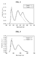
- Example 1-1 and example 1-2 emission spectra were measured and then shown in FIG. 2 , and light emitting efficiencies of R, G, B, and W, driving voltage, and lifespan were measured and then shown in Table 1 below.
- Example 1-2 Example 1-1 Light emitting efficiency (Cd/A) R 14.5 8.4 G 44.2 39.6 B 3.2 3.3 W 90.5 78.5 Driving voltage (10mA/cm 2 ) 11.5 11.4 Lifespan (T95@3000nit) 1000 2300
- the third stack structure was provided with both the red phosphorescent layer and the blue fluorescent layer, thereby improving the entire panel characteristics, and a long-wavelength red phosphorous layer was disposed adjacent to the cathode, thereby improving the light emitting efficiency.
- An organic light emitting diode device was manufactured under the same conditions as the example 1-1 except that the red phosphorescent layer was excluded from the third stack.
- An organic light emitting diode device was manufactured under the same conditions as the example 2-1 except that the green light emitting layer of the second stack was excluded.
- Example 2-1 and example 2-2 emission spectra were measured and then shown in FIG. 3 , and light emitting efficiencies of R, G, B, and W, driving voltage, and lifespan were measured and then shown in Table 2 below.
- Example 2-1 Example 2-2 Light emitting R 7.0 7.1 efficiency (Cd/A) G 40.8 42.3 B 4.2 4.3 W 89.0 91.6
- the second stack was provided with both the yellow-green light emitting layer and the green light emitting layer instead of one yellow-green light emitting layer, thereby improving light emitting efficiency and driving voltage characteristics.
- An organic light emitting diode device was manufactured under the same conditions as the example 1-1 except that the green light emitting layer of the second stack and the red light emitting layer of the third stack were excluded.
- An organic light emitting diode device was manufactured under the same conditions as the example 3-1 except that the hole transport layer and the electron blocking layer of the first stack were formed of a single material to have a thickness of 1150 ⁇ .
- Example 3-1 and example 3-2 emission spectra were measured and then shown in FIG. 4 , and light emitting efficiencies of R, G, B, and W and driving voltage were measured and then shown in Table 3 below.
- Example 3-1 Example 3-2 Light emitting efficiency (Cd/A) R 7.9 8.4 G 34.6 34.4 B 4.2 4.1 W 81.1 82.4 Driving voltage (10mA/cm 2 ) 12.1 12.1
- the hole transport layer and the electron blocking layer of the first stack were formed as a single layer, thereby lowering the thickness of the organic light emitting diode device and improving the light emitting efficiency.
- An organic light emitting diode device was manufactured under the same conditions as the example 3-1 except that the blue light emitting layer of the firs stack and the blue light emitting layer of the third stack each were formed of an anthracene-based host material with a thickness of 100 ⁇ and a pyrene-based compound with a doping concentration of 5% as a dopant.
- An organic light emitting diode device was manufactured under the same conditions as the example 3-1 except that the blue light emitting layer of the first stack was formed of an anthracene-based host material with a thickness of 100 ⁇ , another anthracene-based host material with a thickness of 100 ⁇ , and a pyrene-based compound with a doping concentration of 5% as a dopant, and the blue light emitting layer of the third stack was formed of an anthracene-based host material with a thickness of 100 ⁇ , another anthracene-based host material with a thickness of 100 ⁇ , and a pyrene-based compound with a doping concentration of 5% as a dopant.
- An organic light emitting diode device was manufactured under the same conditions as the example 3-1 except that the blue light emitting layer of the first stack was formed of an anthracene-based host material with a thickness of 100 ⁇ , another anthracene-based host material with a thickness of 100 ⁇ , and a pyrene-based compound with a doping concentration of 5% as a dopant, and the blue light emitting layer of the third stack was formed of an anthracene-based host material with a thickness of 100 ⁇ and a pyrene-based compound with a doping concentration of 5% as a dopant.
- An organic light emitting diode device was manufactured under the same conditions as the example 3-1 except that the blue light emitting layer of the first stack was formed of an anthracene-based host material with a thickness of 100 ⁇ and a pyrene-based compound material with a doping concentration of 5% as a dopant, and the blue light emitting layer of the third stack was formed of an anthracene-based host material with a thickness of 100 ⁇ , another anthracene-based host material with a thickness of 100 ⁇ , and a pyrene-based compound with a doping concentration of 5% as a dopant.
- Example 4-1 Example 4-2
- Example 4-3 Example 4-4 Light emitting efficiency (Cd/A)
- the driving voltage and the lifespan were further improved when the blue light emitting layer adopts a single host as compared with when the blue light emitting layer adopts two hosts.
- An organic light emitting diode device was manufactured under the same conditions as the example 1-1 except that the green light emitting layer of the second stack and the red light emitting layer of the third stack were excluded.
- An organic light emitting diode device was manufactured under the same conditions as the example 5-1 except that two electron transport layers of the third stack were co-deposited as a single layer with a thickness of 360 ⁇ .
- Example 5-1 and example 5-2 emission spectra were measured and then shown in FIG. 6 , and light emitting efficiencies of R, G, B, and W, driving voltage, and lifespan were measured and then shown in Table 5 below.
- Example 5-1 Example 5-2 Light emitting efficiency (Cd/A) R 43.6 44.8 G 4.3 4.4 B 91.9 94.9 W 27.3 28.3 Lifespan (T95@3000nit) 3700 4100 Driving voltage (10mA/cm 2 ) 12.2 12.4
- the materials for the two hole transport layers of the third stack were mixed and then used to form a single layer, thereby lowering the thickness of the organic light emitting diode device and improving the lifespan and driving voltage characteristics.
- An organic light emitting diode device was manufactured under the same conditions as the example 1-1 except that the green light emitting layer of the second stack and the red light emitting layer of the third stack were excluded.
- An organic light emitting diode device was manufactured under the same conditions as the example 6-1 except that the electron blocking layer, the hole transport layer, and the P-type charge generation layer of the second stack were formed as a single layer by forming an aryl amine and carbazole-based host material with a thickness of 50 ⁇ and a P-type dopant compound with a doping concentration of 10%, and then depositing the same aryl amine-based host material with a thickness of 250 ⁇ .
- Example 6-1 and example 6-2 emission spectra were measured and then shown in FIG. 7 , and light emitting efficiencies of R, G, B, and W, driving voltage, and lifespan were measured and then shown in Table 6 below.
- Example 6-1 Light emitting efficiency (Cd/A) R 7.1 7.8 G 41.0 37.9 B 4.2 4.2 W 89.7 86.2 Driving voltage (10mA/cm 2 ) 12.2 12.0 Lifespan (T95, h) R 1300 1800 G 1400 1800 B 2900 3100 W 2100 2700
- the thickness of the organic light emitting diode device was lowered and the lifespan and driving voltage characteristics were further improved when the electron blocking layer, the hole transport layer, and the P-type charge generation layer of the second stack were formed as a single layer of P-type doping layer, as compared with when the respective layers were formed in the second stack.
- An organic light emitting diode device was manufactured under the same condition as the example 6-2.
- An organic light emitting diode device was manufactured under the same conditions as the example 7-1 except that the electron blocking layer, the hole transport layer, and the P-type charge generation layer of the third stack were formed as a single layer by forming an aryl amine and carbazole-based host material with a thickness of 50 ⁇ and a P-type dopant compound with a doping concentration of 10%, and then depositing the same aryl amine-based host material with a thickness of 250 ⁇ .
- An organic light emitting diode device was manufactured under the same conditions as the example 7-2 except that a host different from the aryl amine-based host was used.
- Example 7-1 Example 7-2
- Example 7-3 Light R 7.8 7.6 7.6 emitting efficiency (Cd/A) G 36.1 37.3 37.1 B 4.1 4.1 4.1 W 83.5 84.8 84.5
- the thickness of the organic light emitting diode device was lowered and the lifespan and driving voltage characteristics were further improved when the electron blocking layer, the hole transport layer, and the P-type charge generation layer of the third stack were formed of a single layer of P-type doping layer, together with the second stack, as compared with when the respective were formed in the third stack.
- An organic light emitting diode device was manufactured under the same conditions as the example 6-2 except that the yellow-green phosphorescent light emitting layer and the green phosphorescent layer each were formed of one heteroaryl-based host material with a thickness of 120 ⁇ , another host material with a thickness of 120 ⁇ , and an iridium compound with a doping concentration of 8% as a dopant.
- An organic light emitting diode device was manufactured under the same conditions as the example 8-1 except that, instead of the heteroaryl-based host, a compound of which the LUMO level gap from the electron transport layer is 0.3 eV or smaller was used as a host.
- Example 8-1 and example 8-2 emission spectra were measured and then shown in FIG. 9 , and light emitting efficiencies of R, G, B, and W, driving voltage, and lifespan were measured and then shown in Table 8 below.
- Example 8-1 Light emitting efficiency (Cd/A) R 6.2 6.3 G 32.9 34.0 B 3.9 3.9 W 73.8 76.1 Driving voltage (10mA/cm 2 ) 12.6 13.2 Lifespan (T95, h) R 3600 4800 G 4200 6000 B 3400 3800 W 4200 5600
- An organic light emitting diode device was manufactured under the same condition as the example 6-2 except that the thickness of the electron transport layer of the first stack was 70 ⁇ .
- An organic light emitting diode device was manufactured under the same condition as the example 9-1 except that the thickness of the electron transport layer of the first stack was 110 ⁇ .
- An organic light emitting diode device was manufactured under the same condition as the example 9-1 except that the thickness of the electron transport layer of the first stack was 150 ⁇ .
- Example 9-1 Example 9-2
- Example 9-3 Light emitting efficiency (Cd/A)
- An organic light emitting diode device was manufactured under the same condition as the example 6-2 except that the thickness of the N-type charge generation layer of the first stack was 80 ⁇ .
- An organic light emitting diode device was manufactured under the same condition as the example 10-1 except that the thickness of the N-type charge generation layer of the first stack was 120 ⁇ .
- An organic light emitting diode device was manufactured under the same condition as the example 10-1 except that the thickness of the N-type charge generation layer of the first stack was 150 ⁇ .
- Example 10-1 Example 10-2
- Example 10-3 Light emitting efficiency (Cd/A)
- Driving voltage (10mA/cm 2 ) 12.0 12.0 12.0 Lifespan (T95, h)
- the thickness of the N-type charge generation layer of the first stack becomes greater, the lifespan was increased, but the thickness thereof is preferably 300 ⁇ or smaller.
- An organic light emitting diode device was manufactured under the same condition as the example 6-2 except that the thickness of the electron transport layer of the second stack was 480 ⁇ .
- An organic light emitting diode device was manufactured under the same condition as the example 11-1 except that the thickness of the electron transport layer of the second stack was 350 ⁇ .
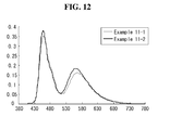
- Example 11-1 Example 11-2 Light emitting efficiency (Cd/A) R 7.9 7.7 G 33.4 34.4 B 4.3 4.3 W 79.0 80.2 Driving voltage (10mA/cm 2 ) 12.2 11.9 Lifespan (T95, h) R 1100 1500 G 1300 1600 B 1900 2000 W 1900 2400
- the organic light emitting diode device includes at least three stacks, at least two blue light emitting layers, and one yellow-green light emitting layer, thereby improving the lifespan and light emitting efficiencies and improving driving voltage characteristics, and realizing white color.
- the distance between the first electrode and the second electrode is 2500 to 5000 ⁇ and the distance between the second electrode 380 and the second light emitting layer is 2000 ⁇ or greater, thereby securing the viewing angle of the image and the light emitting efficiency of the red light.
Landscapes
- Physics & Mathematics (AREA)
- Optics & Photonics (AREA)
- Electroluminescent Light Sources (AREA)
Abstract
Description
- Embodiments of the invention relates to an organic light emitting diode device, and more particularly, to a tandem organic light emitting diode device.
- Recently, flat panel displays (FPDs) are becoming increasingly important with the development of multimedia. Accordingly, several planar display devices, such as a liquid crystal display (LCD), a plasma display panel (PDP), a field emission display (FED), and an organic light emitting diode (OLED) device have been practical. In particular, the OLED device has a high-speed response of 1 ms or less, low power consumption, and self-light emitting characteristics. Also, the OLED device has a merit as a moving picture display media irrespective of the size of the display since it does not have a viewing angle problem. Further, the OLED device is being considered as a next generation flat panel display because it can be fabricated at a low temperature and is simply manufactured based on an existing semiconductor process technology.
- The OLED device includes a light emitting layer between a first electrode and a second electrode. Here, a hole supplied from the first electrode is coupled with an electron received from the second electrode in the light emitting layer to form exciton, and a light is emitted by the energy generated while the exciton returns to the ground state.
- The OLED device has been developed to have various structures, among which a tandem type white OLED device is becoming a concern. In the tandem OLED device, respective layers between the first electrode and the second electrode are deposited without masks, and the organic layers including light emitting layers are sequentially formed by depositing different compositions under vacuum conditions. In this white OLED device, a white light is implemented by mixing colors of two or more light emitting layers. In this case, different light emitting layers that emit multiple color lights are provided between the first electrode and the second electrode, and stacks are differentiated based on a basic structure in which a charge generation layer is provided between each two adjacent light emitting layers.
- However, the tandem white OLED device has problems in that the multiple light emitting layers respectively emitting different colors make it difficult to implement a white light through the control of the light emitting efficiencies among the colors, and the light emitting efficiencies need to be improved.
- Embodiments of the invention provides an organic light emitting diode device capable of improving lifespan, light emitting efficiency, and driving voltage characteristics.
- In one aspect, there is a white organic light emitting diode device, comprising first and second electrodes facing each other above a substrate, first and second charge generation layers formed between the first electrode and the second electrode, a first stack disposed between the first electrode and the first charge generation layer and including a first light emitting layer, a second stack disposed between the first charge generation layer and the second charge generation layer and including a second light emitting layer, and a third stack disposed between the second charge generation layer and the second electrode and including a third light emitting layer, wherein two of the first to third light emitting layers emit a blue light and the rest light emitting layer emits a yellow-green light.
- In one or more embodiments, at least one of the first charge generation layer and the second charge generation layer has a junction structure of an N-type charge generation layer and a P-type charge generation layer.
- In one or more embodiments, the first light emitting layer is a blue fluorescent layer.
- In one or more embodiments, the first to third light emitting layers have a structure in which two dopants are mixed with one host and two dopants are mixed with two hosts.
- In one or more embodiments, in the two hosts, one is an electron transportive host and the other is a hole transportive host.
- In one or more embodiments, at least one of the second light emitting layer and the third light emitting layer has a two-layer structure.
- In one or more embodiments, the first to third stacks each further include a hole transport layer and an electron blocking layer.
- In one or more embodiments, the hole transport layer and the electron blocking layer are formed as a single layer.
- In one or more embodiments, the third stack further includes an electron transport layer disposed between the third light emitting layer and the second electrode and adjoining the third light emitting layer, the electron transport layer containing an electron injection material mixed with a hole blocking material.
- In one or more embodiments, the distance between the first electrode and the second electrode is 2500 to 5000 Å.
- In one or more embodiments, the distance between the second electrode and the second light emitting layer is 2000 Å or greater.
- In one or more embodiments, at least one of the two light emitting layers emitting a blue light further includes a light emitting layer emitting a red light.
- In one or more embodiments, each layer of the two-layer structure has a thickness of 400 Å or smaller.
- The accompanying drawings, which are included to provide a further understanding of the invention and are incorporated in and constitute a part of this specification, illustrate embodiments of the invention and together with the description serve to explain the principles of the invention. In the drawings:
-
FIG. 1 is a diagram showing an organic light emitting diode device according to an embodiment of the present invention; -
FIG. 2 is a graph showing emission spectra measured according to Examples 1-1 and 1-2 of the present invention; -
FIG. 3 is a graph showing emission spectra measured according to Examples 2-1 and 2-2 of the present invention; -
FIG. 4 is a graph showing emission spectra measured according to Examples 3-1 and 3-2 of the present invention; -
FIG. 5 is a graph showing emission spectra measured according to Examples 4-1 to 4-4 of the present invention; -
FIG. 6 is a graph showing emission spectra measured according to Examples 5-1 and 5-2 of the present invention; -
FIG. 7 is a graph showing emission spectra measured according to Examples 6-1 and 6-2 of the present invention; -
FIG. 8 is a graph showing emission spectra measured according to Examples 7-1 to 7-3 of the present invention; -
FIG. 9 is a graph showing emission spectra measured according to Examples 8-1 and 8-2 of the present invention; -
FIG. 10 is a graph showing emission spectra measured according to Examples 9-1 to 9-3 of the present invention; -
FIG. 11 is a graph showing emission spectra measured according to Examples 10-1 to 10-3 of the present invention; and -
FIG. 12 is a graph showing emission spectra measured according to Examples 11-1 and 11-2 of the present invention. - Reference will now be made in detail to embodiments of the invention, examples of which are illustrated in the accompanying drawings. Wherever possible, the same reference numbers will be used throughout the drawings to refer to the same or like parts. It will be paid attention that detailed description of known arts will be omitted if it is determined that the arts can mislead the embodiments of the invention.
-
FIG. 1 is a diagram showing an organic light emitting diode device according to an embodiment of the present invention. - Referring to
FIG. 1 , an organic lightemitting diode device 10 of the present invention includes stacks ST1, ST2, and ST3 positioned between afirst electrode 100 and asecond electrode 380 above asubstrate 50, and includes a firstcharge generation layer 160 and a secondcharge generation layer 250 each positioned between each two of stacks ST1, ST2, and ST3. - More specifically, the
substrate 50 is formed of a light-transmissible transparent glass, a plastic material, or a conductive material. Thefirst electrode 100 positioned on thesubstrate 50 is an anode electrode, and formed of any one of indium tin oxide (ITO), indium zinc oxide (IZO), and zinc oxide (ZnO). - The first stack ST1 positioned on the
first electrode 100 constitutes one light emitting device unit, and includes a firstlight emitting layer 140. The firstlight emitting layer 140 may consist of at least a light emitting layer emitting a blue light, or may further include a light emitting layer emitting a red light. Here, the firstlight emitting layer 140 emitting a blue light may be formed of a fluorescent or phosphorescent material. For example, when the firstlight emitting layer 140 is formed of a fluorescent material, it may include an anthracene derivative, a stylvene derivative, a pyrene derivative, or a carbazole derivative. As the stylvene derivative, compounds represented by the following chemical formulas may be used: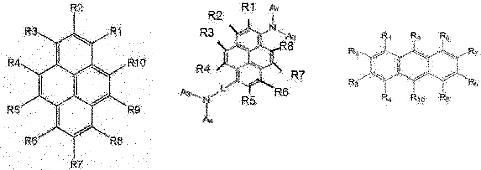
- In the above chemical formulas, Rn (n = 1∼10) may be selected from the group consisting of a substituted or unsubstituted aryl group with 6 to 24 carbon atoms, a substituted or unsubstituted condensed aryl group with 10 to 30 carbon atoms, a substituted or unsubstituted heteroaryl group with 2 to 24 carbon atoms, a substituted or unsubstituted alkyl group with 1 to 24 carbon atoms, a substituted or unsubstituted heteroalkyl group with 1 to 24 carbon atoms, a substituted or unsubstituted cycloalkyl group with 3 to 24 carbon atoms, a substituted or unsubstituted alkoxy group with 1 to 24 carbon atoms, a substituted or unsubstituted aryloxy group with 6 to 24 carbon atoms, a substituted or unsubstituted alkylsilyl group with 1 to 24 carbon atoms, a substituted or unsubstituted arylsilyl group with 6 to 24 carbon atoms, a cyano group, a halogen group, deuterium, and hydrogen; and the aryl group may be selected from the group consisting of phenyl, naphthalene, fluorene, carbazole, phenazine, phenanthroline, phenanthridine, acridine, cinnoline, quinazoline, quinoxaline, naphthydrine, phtalazine, quinolizine, indole, indazole, pyridazine, pyrazine, pyrimidine, pyridine" pyrazole, imidazole, and pyrrole.
- Each L is independently a substituted or unsubstituted aryl group with 6 to 40 carbon atoms or a substituted or unsubstituted heteroaryl group with 3 to 20 carbon atoms; each of substituents of L and A1 to A4 may be selected from the group consisting of a substituted or unsubstituted alkyl group with 1 to 24 carbon atoms, a substituted or unsubstituted cycloalkyl group with 3 to 24 carbon atoms, a substituted or unsubstituted alkoxy group with 1 to 24 carbon atoms, a cyano group, a halogen group, a substituted or unsubstituted aryl group with 6 to 24 carbon atoms, a substituted or unsubstituted aryloxy group with 6 to 24 carbon atoms, a substituted or unsubstituted heteroaryl group with 2 to 24 carbon atoms, a substituted or unsubstituted aryl amino group with 6 to 40 carbon atoms, a substituted or unsubstituted alkyl amino group with 2 to 40 carbon atoms, a germanium group, a boron group, a substituted or unsubstituted alkylsilyl group with 1 to 24 carbon atoms, a substituted or unsubstituted arylsilyl group with 6 to 40 carbon atoms, and deuterium.
- In addition, for example, when the first
light emitting layer 140 is formed of a phosphorescent material, a host may include an anthracene derivative, a stylvene derivative, a pyrene derivative, or a carbazole derivative. As a substituent of the host, compounds represented by the following chemical formulas may be used:
- In the above chemical formulas, Rn (n = 1∼12) may be selected from the group consisting of a substituted or unsubstituted aryl group with 6 to 24 carbon atoms, a substituted or unsubstituted condensed aryl group with 10 to 30 carbon atoms, a substituted or unsubstituted heteroaryl group with 2 to 24 carbon atoms, a substituted or unsubstituted alkyl group with 1 to 24 carbon atoms, a substituted or unsubstituted heteroalkyl group with 1 to 24 carbon atoms, a substituted or unsubstituted cycloalkyl group with 3 to 24 carbon atoms, a substituted or unsubstituted alkoxy group with 1 to 24 carbon atoms, a substituted or unsubstituted aryloxy group with 6 to 24 carbon atoms, a substituted or unsubstituted alkylsilyl group with 1 to 24 carbon atoms, a substituted or unsubstituted arylsilyl group with 6 to 24 carbon atoms, a cyano group, a halogen group, deuterium, and hydrogen; and R1 to R12 may form a condensed ring together with a neighboring substituent.
- The substituent may be a substituted or unsubstituted, fused or unfused aryl group, and may be formed by one to five multiple substitutions or non-multiple substitutions on a core structure consisting of phenyl, naphthalene, fluorene, carbazole, phenazine, phenanthroline, phenanthridine, acridine, cinnoline, quinazoline, quinoxaline, naphthydrine, phtalazine, quinolizine, indole, indazole, pyridazine, pyrazine, pyrimidine, pyridine, pyrazole, imidazole, or pyrrole.
- As a dopant, materials represented by the following chemical formulas may be used. Particularly, metal compounds in which three of N-N, N-O or O-O bonds coordinate to the central metal Ir as shown below may be used.

- The first
light emitting layer 140 may contain one host and one dopant or two hosts and one dopant. Here, between the two hosts, one may be a hole transportive host and the other may be an electron transportive host. As the hole transportive host, a material of the forgoing hole transport layer may be used, and as the electron transportive host, a material of the electron transport layer may be used. - Meanwhile, when the first
light emitting layer 140 further includes a light emitting layer emits a red light, the red light emitting layer may contain, for example, at least one host selected from CBP (4,4'-N,N'-dicarbazolebiphenyl) and Balq (Bis(2-methyl-8-quinlinolato-N1,08)-(1,1'-Biphenyl-4-olato)aluminium), and at least one red phosphorescent dopant selected from Ir(Mnpy)3, Btp2Ir(acac)(bis(20-benzo[4,5-a]thienyl)pyridinato-N,C3O)iridium(zcetylactonate), and Btp2Ir(acac)(iridium(III)bis(1-phenylisoquinolyl)-N,C2')acetyl. - The blue light emitting layer or the red light emitting layer of the first
light emitting layer 140 may contain one host and one dopant or two hosts and one dopant. In addition, when the firstlight emitting layer 140 has a lamination structure of a blue light emitting layer and a red light emitting layer, the red light emitting layer may be disposed on the blue light emitting layer or the blue light emitting layer may be disposed on the red light emitting layer. - Meanwhile, the first stack (ST1) may further include a hole injection layer (HIL) 110, a first hole transport layer (HTL) 120, and a first electron blocking layer (EBL) 130, between the
first electrode 100 and the firstlight emitting layer 140. Thehole injection layer 110 may serve to facilitate the injection of holes into the firstlight emitting layer 140 from thefirst electrode 110, and may be formed of at least one selected from the group consisting of CuPc (cupper phthalocyanine), PEDOT (poly(3,4)-ethylenedioxythiophene), PANI (polyaniline), and NPD (N,N-dinaphthyl-N,N'-diphenyl benzidine), but is not limited thereto. - The first
hole transport layer 120 may serve to facilitate the transport of holes, and may be formed of at least one selected from the group consisting of NPD (N,N-dinaphthyl-N,N'-diphenyl benzidine), TPD (N,N'-bis-(3-methylphenyl)-N,N'-bis-(phenyl)-benzidine), s-TAD, and MTDATA (4,4',4"-Tris(N-3-methylphenyl-N-phenyl-amino)-triphenylamine), but is not limited thereto. For example, the firsthole transport layer 120 may be formed of a compound represented by the following chemical formula:
- Wherein A and B may be selected from compounds represented by the following chemical formulas:

- In the above chemical formulas, Rn (n = 1∼12) may be selected from the group consisting of a substituted or unsubstituted aryl group with 6 to 24 carbon atoms, a substituted or unsubstituted condensed aryl group with 10 to 30 carbon atoms, a substituted or unsubstituted heteroaryl group with 2 to 24 carbon atoms, a substituted or unsubstituted alkyl group with 1 to 24 carbon atoms, a substituted or unsubstituted heteroalkyl group with 1 to 24 carbon atoms, a substituted or unsubstituted cycloalkyl group with 3 to 24 carbon atoms, a substituted or unsubstituted alkoxy group with 1 to 24 carbon atoms, a substituted or unsubstituted aryloxy group with 6 to 24 carbon atoms, a substituted or unsubstituted alkylsilyl group with 1 to 24 carbon atoms, a substituted or unsubstituted arylsilyl group with 6 to 24 carbon atoms, a cyano group, a halogen group, deuterium, and hydrogen; and R1 to R12 may form a condensed ring together with a neighboring substituent. L represents an aryl group, and may be selected from the group consisting of phenyl, naphthalene, fluorene, carbazole, phenazine, phenanthroline, phenanthridine, acridine, cinnoline, quinazoline, quinoxaline, naphthydrine, phtalazine, quinolizine, indole, indazole, pyridazine, pyrazine, pyrimidine, pyridine, pyrazole, imidazole, and pyrrole.
- The first
electron blocking layer 130 contains a material of the hole transport layer and a metal or a meal compound so as to prevent electrons generated in the light emitting layer from going into the hole transport layer. Therefore, the LUMO level of the first electron blocking layer gets higher, and thus the electrons cannot go over the first electron blocking layer. The firsthole transport layer 120 and the firstelectron blocking layer 130 may be a single layer in which respective materials thereof are mixed. - In addition, the first stack ST1 further includes a first electron transport layer (ETL) 150 on the first
light emitting layer 140. The firstelectron transport layer 150 serves to facilitate the transport of electrons, and may be formed of at least one selected from the group consisting of Alq3(tris(8-hydroxyquinolino)aluminum), PBD, TAZ, spiro-PBD, BAlq, and SAlq, but is not limited thereto. - For example, the first
electron transport layer 150 may be formed of compounds represented by the following chemical formulas:
- Ar1 to Ar4 each represent an aryl group, and may be selected from the group consisting of phenyl, naphthalene, fluorene, carbazole, phenazine, phenanthroline, phenanthridine, acridine, cinnoline, quinazoline, quinoxaline, naphthydrine, phtalazine, quinolizine, indole, indazole, pyridazine, pyrazine, pyrimidine, pyridine, pyrazole, imidazole, and pyrrole In the above chemical formulas, Rn (n = 1∼4) may be selected from the group consisting of a substituted or unsubstituted aryl group with 6 to 24 carbon atoms, a substituted or unsubstituted condensed aryl group with 10 to 30 carbon atoms, a substituted or unsubstituted heteroaryl group with 2 to 24 carbon atoms, a substituted or unsubstituted alkyl group with 1 to 24 carbon atoms, a substituted or unsubstituted heteroalkyl group with 1 to 24 carbon atoms, a substituted or unsubstituted cycloalkyl group with 3 to 24 carbon atoms, a substituted or unsubstituted alkoxy group with 1 to 24 carbon atoms, a substituted or unsubstituted aryloxy group with 6 to 24 carbon atoms, a substituted or unsubstituted alkylsilyl group with 1 to 24 carbon atoms, a substituted or unsubstituted arylsilyl group with 6 to 24 carbon atoms, a cyano group, a halogen group, deuterium, and hydrogen.
- Therefore, the first stack ST1 including the
hole injection layer 110, the firsthole transport layer 120, the firstelectron blocking layer 130, the firstlight emitting layer 140, and the firstelectron transport layer 150 is formed on thefirst electrode 100. - A first charge generation layer (CGL) 160 is disposed on the first stack ST1. The first
charge generation layer 160 may be a PN junction charge generation layer in which a N-type charge generation layer 160N and a P-typecharge generation layer 160P are joined to each other. Here, the PN junctioncharge generation layer 160 generates charges or separating them into holes and electrons, and then injects the charges into the respective light emitting layers. That is, the N-type charge generation layer 160N supplies electrons to the firstlight emitting layer 140 adjoining the first electrode, and the P-typecharge generation layer 160P supplies holes a light emitting layer of the second stack ST2, thereby further improve the light emitting efficiency of the organic light emitting diode device including a plurality of light emitting layers. - Here, the P-type
charge generation layer 160P may be formed of a single material, or a single material doped with a P-type dopant. The P-typecharge generation layer 160P may be formed of at least one single material selected from the group consisting of fluorine-substituted TCNPQ, a TCNPQ derivative having a Cyan group, Radiallene-based compounds, Quinone-based compounds, and compounds represented by Chemical Formula (I):
- Substituents of Chemical Formula (I) above may be compounds represented by Chemical Formula (i) and (ii) below:

- The compounds represented by Chemical Formulas (i) and (ii) above may be substituted with substituents represented by Chemical Formula (a) to (g) below:


- In the above Chemical Formula (I), ar1 and ar2 each may be selected from the group consisting of substituted or unsubstituted phenyl, naphthalene, fluorene, carbazole, phenazine, phenanthroline, phenanthridine, acridine, cinnoline, quinazoline, quinoxaline, naphthydrine, phtalazine, quinolizine, indole, indazole, pyridazine, pyrazine, pyrimidine, pyridine, pyrazole, imidazole, and pyrrole.
- In addition, when the P-type
charge generation layer 160P is doped with a P-type dopant, the P-type dopant may be metal oxide, fluorine-substituted TCNPQ, a TCNPQ derivative having a Cyan group, Radiallene-based compounds, Quinone-based compounds, and compounds represented by the following chemical formulas.
- In the above chemical formulas, Ar may be selected from the group consisting of substituted or unsubstituted phenyl, naphthalene, fluorene, carbazole, phenazine, phenanthroline, phenanthridine, acridine, cinnoline, quinazoline, quinoxaline, naphthydrine, phtalazine, quinolizine, indole, indazole, pyridazine, pyrazine, pyrimidine, pyridine, pyrazole, imidazole, and pyrrole, and compounds represented by R1 to R12 below.
- R1 to R12 may be selected from compounds represented by H, CF3, and compounds represented by the following chemical formulas. In the below, A and B may be selected from H, F, and CF3.

- The N-type charge generation layer 160N may be formed of a metal or an N-type doped organic material. Here, the metal may be one material selected from the group consisting of Li, Na, K, Rb, Cs, Mg, Ca, Sr, Ba, La, Ce, Sm, Eu, Tb, Dy, and Yb. In addition, as an N-type dopant and a host material, which are used in the N-type doped organic material, materials that can be conventionally used may be used. For example, the N-type dopant may be an alkali metal, an alkali metal compound, an alkali earth metal, or an alkali earth metal compound. Specifically, the N-type dopant may be one selected from the group consisting of Cs, K, Rb, Mg, Na, Ca, Sr, Eu, and Yb. The host material may be one material selected from the group consisting of tris(8-hydroxyquinoline) aluminum, triazine, a hydroxyquinoline derivative, a benzazole derivative, and a silole derivative.
- Meanwhile, the second stack ST2 including a second
light emitting layer 230 is disposed on the firstcharge generation layer 160. The secondlight emitting layer 230 includes a light emitting layer emitting a yellow-green light, and may further include a light emitting layer emitting a green light. The present embodiment will be described based on a secondlight emitting layer 230 including a yellow-greenlight emitting layer 230a and a greenlight emitting layer 230b. - The green
light emitting layer 230b may contain at least one host selected from CBP (4,4'-N,N'-dicarbazolebiphenyl) and Balq (Bis(2-methyl-8-quinlinolato-N1,O8)-(1,1'-Biphenyl-4-olato)aluminium), and a green phosphorescent dopant of Ir(ppy)3. The yellow-greenlight emitting layer 230a may contain at least one host selected from CBP (4,4'-N,N'-dicarbazolebiphenyl) and Balq (Bis(2-methyl-8-quinlinolato-N1,O8)-(1,1'-Biphenyl-4-olato)aluminium), and a yellow-green phosphorescent dopant emitting a yellow-green light. Meanwhile, the host materials of the yellow-greenlight emitting layer 230a and the greenlight emitting layer 230b may be the same material as the hole transport layer. - At least one of the yellow-green
light emitting layer 230a and the greenlight emitting layer 230b of the secondlight emitting layer 230 may contain two hosts and one dopant. In addition, when the secondlight emitting layer 230 has a lamination structure of the yellow-greenlight emitting layer 230a and the greenlight emitting layer 230b, the greenlight emitting layer 230b may be disposed on the yellow-greenlight emitting layer 230a or the greenlight emitting layer 230b may be disposed on the yellow-greenlight emitting layer 230a. In addition, the yellow-greenlight emitting layer 230a and the greenlight emitting layer 230b of the secondlight emitting layer 230 may be one single layer. Here, the second light emitting layer with a single layer may be formed by mixing one host with a yellow-green dopant and a green dopant or mixing two hosts with a yellow-green dopant and a green dopant. Here, between the two hosts, one may be a hole transportive host and the other may be an electron transportive host. As the hole transportive host, a material of the forgoing hole transport layer may be used, and as the electron transportive host, a material of the electron transport layer may be used. - In addition, in the second
light emitting layer 230, the peak of the emission spectrum of the yellow-greenlight emitting layer 230a may be present in a wavelength band of 550 to 570 nm, and the peak of the emission spectrum of the greenlight emitting layer 230b may be present in a wavelength band of 530 to 550 nm. Here, the full width half maximum values of the respective spectra have 70 nm or higher, respectively, thereby improving the efficiencies of yellow-green color and green color. - In addition, the yellow-green
light emitting layer 230a and the greenlight emitting layer 230b are formed to have a thickness of 400 Å or thinner, thereby preventing the rise in the driving voltage and improving the light emitting efficiency. In addition, the yellow-greenlight emitting layer 230a and the greenlight emitting layer 230b may have different doping concentrations. The doping concentration may be different or the same between the light emitting layer near to the hole transport layer and the light emitting layer far from the hole transport layer. - The second stack (ST2) further includes a second
hole transport layer 210 and a secondelectron blocking layer 220 between the firstcharge generation layer 160 and the secondlight emitting layer 230. The secondhole transport layer 210 is the same as the firsthole transport layer 120, and they may be formed of different materials or the same material. Also, the secondelectron blocking layer 220 is the same as the firstelectron blocking layer 130, and they may be formed of different materials or the same material. In addition, the second stack ST2 further includes a secondelectron transport layer 240 on the secondlight emitting layer 230. The secondelectron transport layer 240 is the same as the firstelectron transport layer 150 of the first stack ST1, and they may be formed of different materials or the same material. Therefore, the second stack ST2 including the secondhole transport layer 210, the secondelectron blocking layer 220, the secondlight emitting layer 230, and the secondelectron transport layer 240 may be formed on the firstcharge generation layer 160. - A second
charge generation layer 250 may be disposed on the second stack ST2. The secondcharge generation layer 250 may be a PN junction charge generation layer in which an N-type charge generation layer 250N and a P-typecharge generation layer 250P are joined to each other, and may have the same structure as the firstcharge generation layer 160. However, the secondcharge generation layer 250 and the firstcharge generation layer 160 may be formed of different materials. For example, the P-typecharge generation layer 160P of the firstcharge generation layer 160 may be formed of a single material, and the P-typecharge generation layer 250P of the secondcharge generation layer 250 may be formed of a single material doped with a P-type dopant. - Meanwhile, a third stack ST3 including a third light emitting layer 30 is disposed on the second
charge generation layer 250. The thirdlight emitting layer 330 may consist of at least a light emitting layer emitting a blue light, and may further include a light emitting layer emitting a red light. The thirdlight emitting layer 330 may have the same structure as the firstlight emitting layer 140 of the first stack ST1. For example, the thirdlight emitting layer 330 may have a lamination structure of a bluelight emitting layer 330a emitting a blue light and a redlight emitting layer 330b emitting a red light. - The third stack (ST3) further includes a third
hole transport layer 310 and a thirdelectron blocking layer 320 between the secondcharge generation layer 250 and the thirdlight emitting layer 330. The thirdhole transport layer 310 is the same as the firsthole transport layer 120, and they may be formed of different materials or the same material. Also, the thirdelectron blocking layer 320 is the same as the firstelectron blocking layer 130, and they may be formed of different materials or the same material. - In addition, the third stack ST3 further includes, on the third
light emitting layer 330, a thirdelectron transport layer 340, a fourthelectron charge layer 350, and anelectron injection layer 360. The fourelectron transport layer 350 is the same as the firstelectron transport layer 150 of the first stack ST1, and they may be formed of different materials or the same material. The thirdelectron transport layer 340 may be formed by mixing an electron injection material having an excellent electron injection capability and a hole blocking material having an excellent hole blocking capability. Here, the mixing ratio of the electron injection material and the hole blocking material may be in the range of 1:99 to 99:1, and preferably 30:70 to 70:30. - The electron injection layer (EIL) 360 serves to facilitate the injection of electrons, and may be formed of Alq3(tris(8-hydroxyquinolino)aluminum), PBD, TAZ, spiro-PBD, BAlq, or SAlq, but is not limited thereto. In addition, the
electron injection layer 360 may be formed of a metal halide compound, for example, at least one selected from the group consisting of MgF2, LiF, NaF, KF, RbF, CsF, FrF, and CaF2, but is not limited thereto. Therefore, the third stack ST3 including the thirdhole transport layer 310, the thirdelectron blocking layer 320, the thirdlight emitting layer 330, and the thirdelectron transport layer 340, the thirdelectron transport layer 350, and theelectron injection layer 360 may be formed on the secondcharge generation layer 250. - A
second electrode 380 may be disposed on the third stack ST3. Thesecond electrode 380 may be a cathode electrode, and may be formed of aluminum (Al), magnesium (Mg), silver (Ag), or an alloy thereof, which has a low work function. Therefore, an organic light emitting diode device includes the first to third stacks ST1, ST2, and ST3 and the first and second charge generation layers 160 and 250 between thefirst electrode 100 and thesecond electrode 380. - The organic light emitting diode device is manufactured such that the distance between the
first electrode 100 and thesecond electrode 380 is 2500 to 5000 Å and the distance between thesecond electrode 380 and the secondlight emitting layer 230 is at least 2000 Å, thereby securing the viewing angle of the image and the light emitting efficiency of the red light. - Although the present embodiment has been described that the first light emitting layer and the third light emitting layer include a blue light emitting layer and the second light emitting layer includes a yellow-green light emitting layer, the present invention is not limited thereto. The position of the second light emitting layer may be changed with the position of the third light emitting layer.
- Hereinafter, examples of the organic light emitting diode device according to the present invention will be set forth. However, the following examples are provided merely to illustrate the present invention, and thus the present invention is not limited thereto. Various structures and effects of the light emitting diode devices of the present invention will be described through various examples to be set forth below.
- An ITO substrate was patterned to have a light emitting area of 2 mm x 2 mm, and then washed. The substrate was mounted in a vacuum chamber and the base pressure was made to be 1×10⁻⁶ torr. NPD with a thickness of 100 Å for a hole injection layer was formed on an anode ITO. An aryl amine-based material with a thickness of 1200 Å for a hole transport layer was formed thereon, and a carbazole-based material with a thickness of 200 Å for an electron blocking layer was formed thereon. For a blue fluorescent layer, an anthracene-based material with a thickness of 250 Å as a host and a pyrene-based material with a doping concentration of 5% as a dopant were formed thereon. Then, a heteroaryl-based material with a thickness of 200 Å for an electron transport layer was formed thereon, so that a first stack was formed. After that, for an N-type charge generation layer, a heteroaryl-based material with a thickness of 200 Å as a host and an alkali earth metal material with a doping concentration of 3% as a dopant were formed. A heteroaryl-based material with a thickness of 200 Å for a P-type charge generation layer was formed thereon. An aryl amine-based material with a thickness of 200 Å for a hole transport layer of was formed thereon. A carbazole-based material with a thickness of 200 Å for an electron blocking layer was formed. Then, for a yellow-green phosphorescent layer, one heteroaryl-based host material with a thickness of 150 Å, another host material with a thickness of 150 Å, and an iridium compound with a doping concentration of 20% as a dopant were formed. Then, for a green phosphorescent layer, one heteroaryl-based host material with a thickness of 150 Å, another host material with a thickness of 150 Å, and an iridium compound with a doping concentration of 15% as a dopant were formed. Then, a heteroaryl-based material with a thickness of 200 Å for an electron transport layer was formed thereon, so that a second stack was formed. Then, for an N-type charge generation layer, a heteroaryl-based material with a thickness of 200 Å as a host and an alkali earth metal material with a doping concentration of 3% as a dopant were formed. A heteroaryl-based material with a thickness of 200 Å for a P- type charge generation layer was formed, and then an aryl amine-based material with a thickness of 1200 Å for a hole transport layer was formed. In addition, a carbazole-based material with a thickness of 200 Å for an electron blocking layer was formed. Then, for a blue fluorescent layer, an anthracene-based material with a thickness of 200 Å as a host and a pyrene-based material with a doping concentration of 5% as a dopant were formed. Then, for a red phosphorescent layer, a heteroaryl-based host material with a thickness of 100 Å, a carbazole and aryl amine-based host material with a thickness of 100 Å, and an iridium compound with a doping concentration of 3% as a dopant were formed. Then, a heteroaryl-based material with a thickness of 200 Å for an electron transport layer was formed, and then a heteroaryl-based material with a thickness of 200 Å for the electron transport layer was again formed. Then, LiF with a thickness of 10 Å for an electron injection layer was formed, so that a third stack was formed. Then, Al with a thickness of 2000 Å for a cathode was formed, so that an organic light emitting diode device was manufactured.
- An organic light emitting diode device was manufactured under the same conditions as the example 1-1 except that the position of the blue fluorescent layer was changed with the position of the red phosphorescent layer.
- In the example 1-1 and example 1-2, emission spectra were measured and then shown in
FIG. 2 , and light emitting efficiencies of R, G, B, and W, driving voltage, and lifespan were measured and then shown in Table 1 below.[Table 1] Example 1-2 Example 1-1 Light emitting efficiency (Cd/A) R 14.5 8.4 G 44.2 39.6 B 3.2 3.3 W 90.5 78.5 Driving voltage (10mA/cm2) 11.5 11.4 Lifespan (T95@3000nit) 1000 2300 - Referring to
FIG. 2 and Table 1, the third stack structure was provided with both the red phosphorescent layer and the blue fluorescent layer, thereby improving the entire panel characteristics, and a long-wavelength red phosphorous layer was disposed adjacent to the cathode, thereby improving the light emitting efficiency. - An organic light emitting diode device was manufactured under the same conditions as the example 1-1 except that the red phosphorescent layer was excluded from the third stack.
- An organic light emitting diode device was manufactured under the same conditions as the example 2-1 except that the green light emitting layer of the second stack was excluded.
- In the example 2-1 and example 2-2, emission spectra were measured and then shown in
FIG. 3 , and light emitting efficiencies of R, G, B, and W, driving voltage, and lifespan were measured and then shown in Table 2 below.[Table 2] Example 2-1 Example 2-2 Light emitting R 7.0 7.1 efficiency (Cd/A) G 40.8 42.3 B 4.2 4.3 W 89.0 91.6 Driving voltage (10mA/cm2) 11.6 12.1 - Referring to
FIG. 3 and Table 2, the second stack was provided with both the yellow-green light emitting layer and the green light emitting layer instead of one yellow-green light emitting layer, thereby improving light emitting efficiency and driving voltage characteristics. - An organic light emitting diode device was manufactured under the same conditions as the example 1-1 except that the green light emitting layer of the second stack and the red light emitting layer of the third stack were excluded.
- An organic light emitting diode device was manufactured under the same conditions as the example 3-1 except that the hole transport layer and the electron blocking layer of the first stack were formed of a single material to have a thickness of 1150 Å.
- In the example 3-1 and example 3-2, emission spectra were measured and then shown in
FIG. 4 , and light emitting efficiencies of R, G, B, and W and driving voltage were measured and then shown in Table 3 below.[Table 3] Example 3-1 Example 3-2 Light emitting efficiency (Cd/A) R 7.9 8.4 G 34.6 34.4 B 4.2 4.1 W 81.1 82.4 Driving voltage (10mA/cm2) 12.1 12.1 - Referring to
FIG. 4 and Table 3, the hole transport layer and the electron blocking layer of the first stack were formed as a single layer, thereby lowering the thickness of the organic light emitting diode device and improving the light emitting efficiency. - An organic light emitting diode device was manufactured under the same conditions as the example 3-1 except that the blue light emitting layer of the firs stack and the blue light emitting layer of the third stack each were formed of an anthracene-based host material with a thickness of 100 Å and a pyrene-based compound with a doping concentration of 5% as a dopant.
- An organic light emitting diode device was manufactured under the same conditions as the example 3-1 except that the blue light emitting layer of the first stack was formed of an anthracene-based host material with a thickness of 100 Å, another anthracene-based host material with a thickness of 100 Å, and a pyrene-based compound with a doping concentration of 5% as a dopant, and the blue light emitting layer of the third stack was formed of an anthracene-based host material with a thickness of 100 Å, another anthracene-based host material with a thickness of 100 Å, and a pyrene-based compound with a doping concentration of 5% as a dopant.
- An organic light emitting diode device was manufactured under the same conditions as the example 3-1 except that the blue light emitting layer of the first stack was formed of an anthracene-based host material with a thickness of 100 Å, another anthracene-based host material with a thickness of 100 Å, and a pyrene-based compound with a doping concentration of 5% as a dopant, and the blue light emitting layer of the third stack was formed of an anthracene-based host material with a thickness of 100 Å and a pyrene-based compound with a doping concentration of 5% as a dopant.
- An organic light emitting diode device was manufactured under the same conditions as the example 3-1 except that the blue light emitting layer of the first stack was formed of an anthracene-based host material with a thickness of 100 Å and a pyrene-based compound material with a doping concentration of 5% as a dopant, and the blue light emitting layer of the third stack was formed of an anthracene-based host material with a thickness of 100 Å, another anthracene-based host material with a thickness of 100 Å, and a pyrene-based compound with a doping concentration of 5% as a dopant.
- In the examples 4-1 to 4-4, emission spectra were measured and then shown in
FIG. 5 , and light emitting efficiencies of R, G, B, and W, driving voltage, and lifespan were measured and then shown in Table 4 below.[Table 4] Example 4-1 Example 4-2 Example 4-3 Example 4-4 Light emitting efficiency (Cd/A) R 7.8 7.8 7.8 7.8 G 36.7 36.6 37.4 37.3 B 4.2 4.0 4.1 4.2 W 84.2 84.1 85.3 85.3 Driving voltage (10mA/cm2) 12.4 11.8 11.9 12.0 Lifespan (T95, h) R 900 1000 900 1000 G 1000 1100 1000 1100 B 1600 1900 1900 2300 W 1400 1500 1400 1700 - Referring to
FIG. 5 and Table 4, the driving voltage and the lifespan were further improved when the blue light emitting layer adopts a single host as compared with when the blue light emitting layer adopts two hosts. - An organic light emitting diode device was manufactured under the same conditions as the example 1-1 except that the green light emitting layer of the second stack and the red light emitting layer of the third stack were excluded.
- An organic light emitting diode device was manufactured under the same conditions as the example 5-1 except that two electron transport layers of the third stack were co-deposited as a single layer with a thickness of 360 Å.
- In the example 5-1 and example 5-2, emission spectra were measured and then shown in
FIG. 6 , and light emitting efficiencies of R, G, B, and W, driving voltage, and lifespan were measured and then shown in Table 5 below.[Table 5] Example 5-1 Example 5-2 Light emitting efficiency (Cd/A) R 43.6 44.8 G 4.3 4.4 B 91.9 94.9 W 27.3 28.3 Lifespan (T95@3000nit) 3700 4100 Driving voltage (10mA/cm2) 12.2 12.4 - Referring to
FIG. 6 and Table 5, the materials for the two hole transport layers of the third stack were mixed and then used to form a single layer, thereby lowering the thickness of the organic light emitting diode device and improving the lifespan and driving voltage characteristics. - An organic light emitting diode device was manufactured under the same conditions as the example 1-1 except that the green light emitting layer of the second stack and the red light emitting layer of the third stack were excluded.
- An organic light emitting diode device was manufactured under the same conditions as the example 6-1 except that the electron blocking layer, the hole transport layer, and the P-type charge generation layer of the second stack were formed as a single layer by forming an aryl amine and carbazole-based host material with a thickness of 50 Å and a P-type dopant compound with a doping concentration of 10%, and then depositing the same aryl amine-based host material with a thickness of 250 Å.
- In the example 6-1 and example 6-2, emission spectra were measured and then shown in
FIG. 7 , and light emitting efficiencies of R, G, B, and W, driving voltage, and lifespan were measured and then shown in Table 6 below.[Table 6] Example 6-1 Example 6-2 Light emitting efficiency (Cd/A) R 7.1 7.8 G 41.0 37.9 B 4.2 4.2 W 89.7 86.2 Driving voltage (10mA/cm2) 12.2 12.0 Lifespan (T95, h) R 1300 1800 G 1400 1800 B 2900 3100 W 2100 2700 - Referring to
FIG. 7 and Table 6, the thickness of the organic light emitting diode device was lowered and the lifespan and driving voltage characteristics were further improved when the electron blocking layer, the hole transport layer, and the P-type charge generation layer of the second stack were formed as a single layer of P-type doping layer, as compared with when the respective layers were formed in the second stack. - An organic light emitting diode device was manufactured under the same condition as the example 6-2.
- An organic light emitting diode device was manufactured under the same conditions as the example 7-1 except that the electron blocking layer, the hole transport layer, and the P-type charge generation layer of the third stack were formed as a single layer by forming an aryl amine and carbazole-based host material with a thickness of 50 Å and a P-type dopant compound with a doping concentration of 10%, and then depositing the same aryl amine-based host material with a thickness of 250 Å.
- An organic light emitting diode device was manufactured under the same conditions as the example 7-2 except that a host different from the aryl amine-based host was used.
- In the examples 7-1 to 7-3, emission spectra were measured and then shown in
FIG. 8 , and light emitting efficiencies of R, G, B, and W, driving voltage, and lifespan were measured and then shown in Table 7 below.[Table 7] Example 7-1 Example 7-2 Example 7-3 Light R 7.8 7.6 7.6 emitting efficiency (Cd/A) G 36.1 37.3 37.1 B 4.1 4.1 4.1 W 83.5 84.8 84.5 Driving voltage (10mA/cm2) 12.0 11.9 12.9 Lifespan (T95, h) R 2200 2800 2900 G 2500 3100 3200 B 2400 2600 2500 W 2600 3300 3300 - Referring to
FIG. 8 and Table 7, the thickness of the organic light emitting diode device was lowered and the lifespan and driving voltage characteristics were further improved when the electron blocking layer, the hole transport layer, and the P-type charge generation layer of the third stack were formed of a single layer of P-type doping layer, together with the second stack, as compared with when the respective were formed in the third stack. - An organic light emitting diode device was manufactured under the same conditions as the example 6-2 except that the yellow-green phosphorescent light emitting layer and the green phosphorescent layer each were formed of one heteroaryl-based host material with a thickness of 120 Å, another host material with a thickness of 120 Å, and an iridium compound with a doping concentration of 8% as a dopant.
- An organic light emitting diode device was manufactured under the same conditions as the example 8-1 except that, instead of the heteroaryl-based host, a compound of which the LUMO level gap from the electron transport layer is 0.3 eV or smaller was used as a host.
- In the example 8-1 and example 8-2, emission spectra were measured and then shown in
FIG. 9 , and light emitting efficiencies of R, G, B, and W, driving voltage, and lifespan were measured and then shown in Table 8 below.[Table 8] Example 8-1 Example 8-2 Light emitting efficiency (Cd/A) R 6.2 6.3 G 32.9 34.0 B 3.9 3.9 W 73.8 76.1 Driving voltage (10mA/cm2) 12.6 13.2 Lifespan (T95, h) R 3600 4800 G 4200 6000 B 3400 3800 W 4200 5600 - Referring to
FIG. 9 and Table 8, as the LUMO level gap of the host of the green light emitting layer from the electron transport layer becomes smaller, the light emitting efficiency and the lifespan were further improved. - An organic light emitting diode device was manufactured under the same condition as the example 6-2 except that the thickness of the electron transport layer of the first stack was 70 Å.
- An organic light emitting diode device was manufactured under the same condition as the example 9-1 except that the thickness of the electron transport layer of the first stack was 110 Å.
- An organic light emitting diode device was manufactured under the same condition as the example 9-1 except that the thickness of the electron transport layer of the first stack was 150 Å.
- In the examples 9-1 to 9-3, emission spectra were measured and then shown in
FIG. 10 , and light emitting efficiencies of R, G, B, and W, driving voltage, and lifespan were measured and then shown in Table 9 below.[Table 9] Example 9-1 Example 9-2 Example 9-3 Light emitting efficiency (Cd/A) R 7.9 8.1 7.6 G 35.7 35.9 39.0 B 4.1 4.1 4.2 W 82.4 83.1 87.4 Driving voltage (10mA/cm2) 12.0 12.0 12.1 Lifespan (T95, h) R 4400 4000 3900 G 4700 4000 3900 B 3400 3200 3400 W 4600 3800 3900 - Referring to
FIG. 10 and Table 9, as the thickness of the electron transport layer of the first stack becomes smaller, the lifespan was increased and the efficiency was further improved. - An organic light emitting diode device was manufactured under the same condition as the example 6-2 except that the thickness of the N-type charge generation layer of the first stack was 80 Å.
- An organic light emitting diode device was manufactured under the same condition as the example 10-1 except that the thickness of the N-type charge generation layer of the first stack was 120 Å.
- An organic light emitting diode device was manufactured under the same condition as the example 10-1 except that the thickness of the N-type charge generation layer of the first stack was 150 Å.
- In the examples 10-1 to 10-3, emission spectra were measured and then shown in
FIG. 11 , and light emitting efficiencies of R, G, B, and W, driving voltage, and lifespan were measured and then shown in Table 10 below.[Table 10] Example 10-1 Example 10-2 Example 10-3 Light emitting efficiency (Cd/A) R 8.0 8.1 7.5 G 35.5 35.9 38.3 B 4.2 4.1 4.1 W 82.3 83.1 85.8 Driving voltage (10mA/cm2) 12.0 12.0 12.0 Lifespan (T95, h) R 3400 3600 3900 G 3600 4000 4100 B 3000 3200 3300 W 3600 3800 4100 - Referring to
FIG. 11 and Table 10, as the thickness of the N-type charge generation layer of the first stack becomes greater, the lifespan was increased, but the thickness thereof is preferably 300 Å or smaller. - An organic light emitting diode device was manufactured under the same condition as the example 6-2 except that the thickness of the electron transport layer of the second stack was 480 Å.
- An organic light emitting diode device was manufactured under the same condition as the example 11-1 except that the thickness of the electron transport layer of the second stack was 350 Å.
- In the example 11-1 and example 11-2, emission spectra were measured and then shown in
FIG. 12 , and light emitting efficiencies of R, G, B, and W, driving voltage, and lifespan were measured and then shown in Table 11 below.[Table 11] Example 11-1 Example 11-2 Light emitting efficiency (Cd/A) R 7.9 7.7 G 33.4 34.4 B 4.3 4.3 W 79.0 80.2 Driving voltage (10mA/cm2) 12.2 11.9 Lifespan (T95, h) R 1100 1500 G 1300 1600 B 1900 2000 W 1900 2400 - Referring to
FIG. 12 and Table 11, as the thickness of the electron transport layer of the second stack becomes smaller, the lifespan was further increased and the driving voltage was further reduced. - As described above, the organic light emitting diode device according to an embodiment of the present invention includes at least three stacks, at least two blue light emitting layers, and one yellow-green light emitting layer, thereby improving the lifespan and light emitting efficiencies and improving driving voltage characteristics, and realizing white color.
- Further, according to the organic light emitting diode device of the present invention, the distance between the first electrode and the second electrode is 2500 to 5000 Å and the distance between the
second electrode 380 and the second light emitting layer is 2000 Å or greater, thereby securing the viewing angle of the image and the light emitting efficiency of the red light. - Although embodiments have been described with reference to a number of illustrative embodiments thereof, it should be understood that numerous other modifications and embodiments can be devised by those skilled in the art that will fall within the scope of the principles of this disclosure. More particularly, various variations and modifications are possible in the component parts and/or arrangements of the subject combination arrangement within the scope of the disclosure, the drawings and the appended claims. In addition to variations and modifications in the component parts and/or arrangements, alternative uses will also be apparent to those skilled in the art.
Claims (13)
- A white organic light emitting diode device, comprising:first and second electrodes facing each other above a substrate;first and second charge generation layers formed between the first electrode and the second electrode;a first stack disposed between the first electrode and the first charge generation layer and including a first light emitting layer;a second stack disposed between the first charge generation layer and the second charge generation layer and including a second light emitting layer; anda third stack disposed between the second charge generation layer and the second electrode and including a third light emitting layer,wherein two of the first to third light emitting layers emit a blue light and the rest light emitting layer emits a yellow-green light.
- The white organic light emitting diode device of claim 1, wherein at least one of the first charge generation layer and the second charge generation layer has a junction structure of an N-type charge generation layer and a P-type charge generation layer.
- The white organic light emitting diode device of claim 1 or 2, wherein the first light emitting layer is a blue fluorescent layer.
- The white organic light emitting diode device of any one of claims 1 to 3, wherein the first to third light emitting layers have a structure in which two dopants are mixed with one host and two dopants are mixed with two hosts.
- The white organic light emitting diode device of claim 4, wherein in the two hosts, one is an electron transportive host and the other is a hole transportive host.
- The white organic light emitting diode device of any one of claims 1 to 5, wherein at least one of the second light emitting layer and the third light emitting layer has a two-layer structure.
- The white organic light emitting diode device of any one of claims 1 to 6, wherein the first to third stacks each further include a hole transport layer and an electron blocking layer.
- The white organic light emitting diode device of claim 7, wherein the hole transport layer and the electron blocking layer are formed as a single layer.
- The white organic light emitting diode device of any one of claims 1 to 8, wherein the third stack further includes an electron transport layer disposed between the third light emitting layer and the second electrode and adjoining the third light emitting layer, the electron transport layer containing an electron injection material mixed with a hole blocking material.
- The white organic light emitting diode device of any one of claims 1 to 9, wherein the distance between the first electrode and the second electrode is 2500 to 5000 A.
- The white organic light emitting diode device of claim 10, wherein the distance between the second electrode and the second light emitting layer is 2000 Å or greater.
- The white organic light emitting diode device of any one of claims 1 to 11, wherein at least one of the two light emitting layers emitting a blue light further includes a light emitting layer emitting a red light.
- The white organic light emitting diode device of claim 6, wherein each layer of the two-layer structure has a thickness of 400 Å or smaller.
Applications Claiming Priority (1)
| Application Number | Priority Date | Filing Date | Title |
|---|---|---|---|
| KR1020130091063A KR102081605B1 (en) | 2013-07-31 | 2013-07-31 | White organic light emitting diode device |
Publications (3)
| Publication Number | Publication Date |
|---|---|
| EP2833407A2 true EP2833407A2 (en) | 2015-02-04 |
| EP2833407A3 EP2833407A3 (en) | 2015-02-18 |
| EP2833407B1 EP2833407B1 (en) | 2022-10-26 |
Family
ID=50687409
Family Applications (1)
| Application Number | Title | Priority Date | Filing Date |
|---|---|---|---|
| EP14168280.7A Active EP2833407B1 (en) | 2013-07-31 | 2014-05-14 | White organic light emitting diode device |
Country Status (6)
| Country | Link |
|---|---|
| US (1) | US9281487B2 (en) |
| EP (1) | EP2833407B1 (en) |
| JP (1) | JP6018139B2 (en) |
| KR (1) | KR102081605B1 (en) |
| CN (1) | CN104347807B (en) |
| TW (1) | TWI552409B (en) |
Cited By (7)
| Publication number | Priority date | Publication date | Assignee | Title |
|---|---|---|---|---|
| EP2950362A1 (en) * | 2014-05-26 | 2015-12-02 | LG Display Co., Ltd. | White organic light emitting device |
| EP3174117A1 (en) * | 2015-11-30 | 2017-05-31 | LG Display Co., Ltd. | Organic light emitting display device |
| EP3258747A4 (en) * | 2015-03-02 | 2018-03-14 | Lumiotec Inc. | Organic electroluminescent element and lighting device |
| CN108349878A (en) * | 2015-11-17 | 2018-07-31 | 株式会社Lg化学 | Compounds and organic electronic components containing them |
| US10084146B2 (en) | 2015-03-02 | 2018-09-25 | Lumiotec Inc. | Organic electroluminescent element and lighting device |
| EP2924756B1 (en) * | 2014-03-27 | 2020-10-21 | LG Display Co., Ltd. | Organic light emitting device |
| EP3125329B1 (en) * | 2015-07-31 | 2025-08-27 | LG Display Co., Ltd. | Organic light emitting display device |
Families Citing this family (65)
| Publication number | Priority date | Publication date | Assignee | Title |
|---|---|---|---|---|
| JP2526295B2 (en) | 1989-12-13 | 1996-08-21 | 富士通株式会社 | How to make an exposure mask |
| KR102081117B1 (en) * | 2013-08-29 | 2020-02-25 | 엘지디스플레이 주식회사 | White organic light emitting device |
| KR102162259B1 (en) * | 2014-05-26 | 2020-10-07 | 엘지디스플레이 주식회사 | White organic light emitting device |
| KR102302850B1 (en) * | 2014-10-22 | 2021-09-23 | 삼성디스플레이 주식회사 | Light emitting device |
| US9660220B2 (en) * | 2014-10-24 | 2017-05-23 | Semiconductor Energy Laboratory Co., Ltd. | Multiple light-emitting element device |
| KR102294413B1 (en) * | 2014-11-18 | 2021-08-27 | 삼성디스플레이 주식회사 | Organice light emitting diode display |
| CN107004773A (en) * | 2014-12-05 | 2017-08-01 | 保土谷化学工业株式会社 | Organic electroluminescence device |
| TWI682920B (en) * | 2015-01-08 | 2020-01-21 | 日商保土谷化學工業股份有限公司 | Organic electroluminescent element |
| KR102435038B1 (en) * | 2015-03-30 | 2022-08-22 | 엘지디스플레이 주식회사 | Organic light emitting display device |
| CN105161627B (en) | 2015-06-29 | 2016-08-17 | 京东方科技集团股份有限公司 | A kind of series type organic LED, array base palte and display device |
| CN105161628B (en) * | 2015-06-29 | 2017-02-15 | 京东方科技集团股份有限公司 | Tandem-type organic light-emitting diode, array substrate, and display device |
| KR102504145B1 (en) * | 2015-08-21 | 2023-02-27 | 엘지디스플레이 주식회사 | Organic light emitting display device |
| KR102399953B1 (en) | 2015-08-25 | 2022-05-18 | 엘지디스플레이 주식회사 | Organic light emitting display device |
| US10270041B2 (en) * | 2015-08-28 | 2019-04-23 | Semiconductor Energy Laboratory Co., Ltd. | Light-emitting element, light-emitting device, electronic device, and lighting device |
| KR102512714B1 (en) | 2015-09-15 | 2023-03-23 | 삼성디스플레이 주식회사 | Organic emitting display apparatus, method of controlling the apparatus, and computer program for executing the method |
| KR102377466B1 (en) * | 2015-10-29 | 2022-03-21 | 엘지디스플레이 주식회사 | Organic light emitting display apparatus |
| US11594683B2 (en) * | 2015-10-29 | 2023-02-28 | Hodogaya Chemical Co., Ltd. | Organic electroluminescent device |
| KR102574052B1 (en) | 2015-11-19 | 2023-09-04 | 엘지디스플레이 주식회사 | Organic light emitting display device |
| US10374183B2 (en) | 2015-11-19 | 2019-08-06 | Lg Display Co., Ltd. | Organic light emitting display device having layer to control charge transfer |
| US10243175B2 (en) | 2016-02-02 | 2019-03-26 | Samsung Display Co., Ltd. | Organic light-emitting apparatus fabricated using a fluoropolymer and method of manufacturing the same |
| KR102490889B1 (en) * | 2016-02-29 | 2023-01-25 | 삼성디스플레이 주식회사 | Organic light-emitting apparatus and the method for manufacturing of the organic light-emitting display apparatus |
| KR102642369B1 (en) * | 2016-03-25 | 2024-03-05 | 삼성디스플레이 주식회사 | Organic light emitting display device and method of manufacturing the organic light emitting display device |
| KR102553276B1 (en) * | 2016-03-29 | 2023-07-06 | 엘지디스플레이 주식회사 | Organic light emitting display device |
| KR102774157B1 (en) * | 2016-05-12 | 2025-02-28 | 삼성디스플레이 주식회사 | Organic light emitting device |
| CN106410049A (en) * | 2016-06-02 | 2017-02-15 | 深圳市华星光电技术有限公司 | OLED device and OLED display |
| KR102611206B1 (en) * | 2016-07-13 | 2023-12-08 | 삼성디스플레이 주식회사 | Organic light emitting device |
| KR20180013536A (en) * | 2016-07-29 | 2018-02-07 | 엘지디스플레이 주식회사 | White Organic Lighting Emitting Device and Organic Lighting Display Device Using the Same |
| KR102715632B1 (en) | 2016-09-27 | 2024-10-11 | 삼성디스플레이 주식회사 | Organic electroluminescence display device |
| KR102635062B1 (en) * | 2016-09-30 | 2024-02-07 | 엘지디스플레이 주식회사 | Organic compound and light emitting diode and organic light emitting diode display device using the same |
| KR102714659B1 (en) | 2016-12-09 | 2024-10-07 | 엘지디스플레이 주식회사 | Electronic device |
| US10424756B2 (en) | 2017-06-22 | 2019-09-24 | Shenzhen China Star Optoelectronics Technology Co., Ltd | Flexible display apparatus and its white light organic electroluminescent device |
| CN107359261A (en) * | 2017-06-22 | 2017-11-17 | 深圳市华星光电技术有限公司 | Flexible display apparatus and its white light organic electroluminescent device |
| KR102337204B1 (en) * | 2017-06-30 | 2021-12-07 | 엘지디스플레이 주식회사 | Organic light emitting diode and display device comprising the same |
| KR102395782B1 (en) * | 2017-07-31 | 2022-05-09 | 삼성전자주식회사 | Organic light emitting device |
| KR102347450B1 (en) * | 2017-09-12 | 2022-01-04 | 엘지디스플레이 주식회사 | Organic light emitting diode and organic light emitting display device comprising the same |
| US10770673B2 (en) * | 2017-11-28 | 2020-09-08 | The Regents Of The University Of Michigan | Highly reliable stacked white organic light emitting device |
| KR102476814B1 (en) * | 2017-12-12 | 2022-12-12 | 엘지디스플레이 주식회사 | Illumination Device |
| KR102522288B1 (en) * | 2018-03-13 | 2023-04-19 | 삼성디스플레이 주식회사 | Organic light emitting diode device, and compound for charge gernation layer included therein |
| JP2021182459A (en) * | 2018-06-04 | 2021-11-25 | 出光興産株式会社 | Organic electroluminescence devices and electronic devices |
| TWI703722B (en) * | 2018-08-06 | 2020-09-01 | 友達光電股份有限公司 | Light emitting device |
| KR102557743B1 (en) | 2018-08-14 | 2023-07-19 | 엘지디스플레이 주식회사 | Organic light emitting diodes display |
| KR102653732B1 (en) * | 2018-10-10 | 2024-04-01 | 엘지디스플레이 주식회사 | Organic compounds, organic light emitting diode and organic light emitting device having the compounds |
| KR102690956B1 (en) * | 2018-11-20 | 2024-07-31 | 엘지디스플레이 주식회사 | Organic Light Emitting Diode Display Device |
| EP3670510A3 (en) * | 2018-12-20 | 2020-07-01 | Duk San Neolux Co., Ltd. | Benzo[b]naphtho[2,3-d]furanyl- or benzo[b]naphtho[2,3-d]thiophenyl-triazine compounds for organic electronic elements |
| CN109742252B (en) * | 2019-01-08 | 2020-12-29 | 京东方科技集团股份有限公司 | A display panel and display device |
| KR102806840B1 (en) * | 2019-06-27 | 2025-05-16 | 삼성전자주식회사 | Display device |
| US10937983B2 (en) * | 2019-06-28 | 2021-03-02 | Wuhan China Star Optoelectronics Semiconductor Display Technology Co., Ltd. | Organic electroluminescent device and display panel |
| KR102500996B1 (en) * | 2019-07-12 | 2023-02-20 | 삼성디스플레이 주식회사 | Light emitting diode and display panel having the same |
| CN110957347A (en) * | 2019-12-13 | 2020-04-03 | 苏州星烁纳米科技有限公司 | Light-emitting structure, display device and lighting device |
| EP4651686A3 (en) | 2020-01-28 | 2026-02-25 | OLEDWorks LLC | Stacked oled microdisplay with low-voltage silicon backplane |
| EP3878924A1 (en) * | 2020-03-12 | 2021-09-15 | Lumileds LLC | Nitridophosphate phosphors for solid state lighting and method of production |
| KR20210141793A (en) * | 2020-05-12 | 2021-11-23 | 삼성디스플레이 주식회사 | Organic light emitting device and device including the same |
| CN111668381B (en) * | 2020-06-19 | 2023-01-24 | 京东方科技集团股份有限公司 | Display substrate, preparation method thereof and display device |
| KR102821338B1 (en) * | 2020-08-07 | 2025-06-18 | 삼성디스플레이 주식회사 | light emitting device and electronic device including the light emitting device |
| KR102866834B1 (en) | 2020-08-19 | 2025-09-30 | 오엘이디워크스 엘엘씨 | Pixel circuitry for crosstalk reduction |
| KR102363914B1 (en) | 2020-08-20 | 2022-02-17 | 삼성디스플레이 주식회사 | Light emitting device and electronic device including the same |
| KR102821745B1 (en) * | 2020-08-20 | 2025-06-18 | 삼성디스플레이 주식회사 | Light emitting device and electronic device including the same |
| CN112467049A (en) * | 2020-11-18 | 2021-03-09 | 安徽熙泰智能科技有限公司 | Structure of OLED device |
| KR102950519B1 (en) * | 2020-12-23 | 2026-04-08 | 엘지디스플레이 주식회사 | Organic Light Emitting Diode Display Device |
| KR102906667B1 (en) * | 2020-12-31 | 2025-12-31 | 엘지디스플레이 주식회사 | White Light Emitting Device and Light Emitting Display Device Using the Same |
| DE102021134506A1 (en) * | 2020-12-31 | 2022-06-30 | Lg Display Co., Ltd. | Display device with a light-emitting device |
| CN112967680B (en) * | 2021-03-18 | 2022-12-16 | 合肥京东方卓印科技有限公司 | Pixel structure, driving method thereof and display substrate |
| KR102847825B1 (en) * | 2021-04-08 | 2025-08-20 | 삼성디스플레이 주식회사 | Light emitting device and display apparatus including the same |
| KR102859905B1 (en) * | 2021-06-24 | 2025-09-15 | 삼성디스플레이 주식회사 | Light emitting device and display device comprising the same |
| TWI871517B (en) | 2021-07-20 | 2025-02-01 | 美商Oled沃克斯有限責任公司 | Display with three regions of color space |
Family Cites Families (33)
| Publication number | Priority date | Publication date | Assignee | Title |
|---|---|---|---|---|
| US5274248A (en) * | 1991-06-05 | 1993-12-28 | Matsushita Electric Industrial Co., Ltd. | Light-emitting device with II-VI compounds |
| JP3065494B2 (en) * | 1994-12-02 | 2000-07-17 | 東芝ライテック株式会社 | Fluorescent lamp and color liquid crystal display using the same |
| US5552253A (en) * | 1995-03-31 | 1996-09-03 | Xerox Corporation | Multiple layer photoreceptor for color xerography |
| US5727014A (en) * | 1995-10-31 | 1998-03-10 | Hewlett-Packard Company | Vertical-cavity surface-emitting laser generating light with a defined direction of polarization |
| US6090511A (en) * | 1998-08-21 | 2000-07-18 | Sinonar Corp. | Multi-layered electrophotographic photoreceptors and method for enhancing photosensitivity thereof |
| JP2001175007A (en) * | 1999-10-20 | 2001-06-29 | Xerox Corp | Photosensitive body, image forming method and image forming device |
| US7158161B2 (en) * | 2002-09-20 | 2007-01-02 | Matsushita Electric Industrial Co., Ltd. | Organic electroluminescence element and an exposure unit and image-forming apparatus both using the element |
| US6936961B2 (en) * | 2003-05-13 | 2005-08-30 | Eastman Kodak Company | Cascaded organic electroluminescent device having connecting units with N-type and P-type organic layers |
| KR100670543B1 (en) * | 2003-12-29 | 2007-01-16 | 엘지.필립스 엘시디 주식회사 | Organic electroluminescent device |
| WO2006085615A1 (en) * | 2005-02-10 | 2006-08-17 | Tohoku Pioneer Corporation | Self-luminous device and self-luminous panel |
| US7494722B2 (en) | 2005-02-23 | 2009-02-24 | Eastman Kodak Company | Tandem OLED having an organic intermediate connector |
| US7750561B2 (en) * | 2005-05-20 | 2010-07-06 | Lg Display Co., Ltd. | Stacked OLED structure |
| US7531959B2 (en) * | 2005-06-29 | 2009-05-12 | Eastman Kodak Company | White light tandem OLED display with filters |
| US7332860B2 (en) * | 2006-03-30 | 2008-02-19 | Eastman Kodak Company | Efficient white-light OLED display with filters |
| WO2008035406A1 (en) * | 2006-09-20 | 2008-03-27 | Pioneer Corporation | Optical device |
| KR101316752B1 (en) * | 2007-05-31 | 2013-10-08 | 삼성디스플레이 주식회사 | White organic light emitting display |
| US7977872B2 (en) * | 2008-09-16 | 2011-07-12 | Global Oled Technology Llc | High-color-temperature tandem white OLED |
| TW201023413A (en) * | 2008-12-05 | 2010-06-16 | Univ Tsinghua | Organic light-emitting diode (OLED) device |
| US20120235131A1 (en) | 2009-11-27 | 2012-09-20 | Sharp Kabushiki Kaisha | Organic electroluminescence element, manufacturing method thereof, and organic electroluminescence display device |
| EP2366753B1 (en) * | 2010-03-02 | 2015-06-17 | Semiconductor Energy Laboratory Co., Ltd. | Light-Emitting Element and Lighting Device |
| KR101097339B1 (en) * | 2010-03-08 | 2011-12-23 | 삼성모바일디스플레이주식회사 | Organic light emitting diode and method for preparing the same |
| TWI567075B (en) * | 2010-06-15 | 2017-01-21 | 國立清華大學 | 6H-吲哚[3,2-b]quinoxaline derivative and organic light-emitting diode thereof |
| JP5653122B2 (en) * | 2010-08-10 | 2015-01-14 | 住友化学株式会社 | Organic electroluminescence device and method for producing the same |
| JP5639181B2 (en) * | 2010-09-24 | 2014-12-10 | 株式会社日立製作所 | Organic light emitting device and light source device using the same |
| US8963143B2 (en) * | 2010-11-09 | 2015-02-24 | Koninklijkle Philips N.V. | Organic electroluminescent device |
| JP2012146764A (en) | 2011-01-11 | 2012-08-02 | Canon Inc | Display device |
| JP6108664B2 (en) * | 2011-04-04 | 2017-04-05 | ローム株式会社 | Organic EL device |
| TWI532822B (en) * | 2011-04-29 | 2016-05-11 | 半導體能源研究所股份有限公司 | Phosphorescent light emitting device, electronic device and lighting device |
| US8884274B2 (en) * | 2011-10-12 | 2014-11-11 | Lg Display Co., Ltd. | White organic light emitting device |
| US8476624B1 (en) * | 2012-06-01 | 2013-07-02 | Au Optronics Corporation | Organic light emitting diode (OLED) device |
| DE102012214021B4 (en) * | 2012-08-08 | 2018-05-09 | Osram Oled Gmbh | Optoelectronic component and method for producing an optoelectronic component |
| US9577221B2 (en) * | 2012-09-26 | 2017-02-21 | Universal Display Corporation | Three stack hybrid white OLED for enhanced efficiency and lifetime |
| DE102013112602B4 (en) * | 2012-12-18 | 2020-11-12 | Lg Display Co., Ltd. | White organic light emitting device |
-
2013
- 2013-07-31 KR KR1020130091063A patent/KR102081605B1/en active Active
-
2014
- 2014-05-14 EP EP14168280.7A patent/EP2833407B1/en active Active
- 2014-07-23 US US14/339,168 patent/US9281487B2/en active Active
- 2014-07-30 TW TW103126094A patent/TWI552409B/en active
- 2014-07-30 JP JP2014154577A patent/JP6018139B2/en active Active
- 2014-07-30 CN CN201410371276.0A patent/CN104347807B/en active Active
Non-Patent Citations (1)
| Title |
|---|
| None |
Cited By (11)
| Publication number | Priority date | Publication date | Assignee | Title |
|---|---|---|---|---|
| EP2924756B1 (en) * | 2014-03-27 | 2020-10-21 | LG Display Co., Ltd. | Organic light emitting device |
| EP2950362A1 (en) * | 2014-05-26 | 2015-12-02 | LG Display Co., Ltd. | White organic light emitting device |
| US9705102B2 (en) | 2014-05-26 | 2017-07-11 | Lg Display Co., Ltd. | White organic light emitting device |
| US10038157B2 (en) | 2014-05-26 | 2018-07-31 | Lg Display Co., Ltd. | White organic light emitting device |
| EP3258747A4 (en) * | 2015-03-02 | 2018-03-14 | Lumiotec Inc. | Organic electroluminescent element and lighting device |
| US10084146B2 (en) | 2015-03-02 | 2018-09-25 | Lumiotec Inc. | Organic electroluminescent element and lighting device |
| EP3125329B1 (en) * | 2015-07-31 | 2025-08-27 | LG Display Co., Ltd. | Organic light emitting display device |
| EP4611510A3 (en) * | 2015-07-31 | 2025-12-10 | LG Display Co., Ltd. | Organic light emitting display device |
| CN108349878A (en) * | 2015-11-17 | 2018-07-31 | 株式会社Lg化学 | Compounds and organic electronic components containing them |
| EP3174117A1 (en) * | 2015-11-30 | 2017-05-31 | LG Display Co., Ltd. | Organic light emitting display device |
| US10950812B2 (en) | 2015-11-30 | 2021-03-16 | Lg Display Co., Ltd. | Organic light emitting display device (OLED) having p-type charge generation layer (CGL) formed between emissions stack |
Also Published As
| Publication number | Publication date |
|---|---|
| CN104347807B (en) | 2017-06-09 |
| TWI552409B (en) | 2016-10-01 |
| KR20150015647A (en) | 2015-02-11 |
| KR102081605B1 (en) | 2020-02-27 |
| CN104347807A (en) | 2015-02-11 |
| EP2833407B1 (en) | 2022-10-26 |
| EP2833407A3 (en) | 2015-02-18 |
| TW201505224A (en) | 2015-02-01 |
| JP6018139B2 (en) | 2016-11-02 |
| JP2015032582A (en) | 2015-02-16 |
| US9281487B2 (en) | 2016-03-08 |
| US20150034923A1 (en) | 2015-02-05 |
Similar Documents
| Publication | Publication Date | Title |
|---|---|---|
| EP2833407B1 (en) | White organic light emitting diode device | |
| KR102679133B1 (en) | Organic Light Emitting Diode Device | |
| US9793489B2 (en) | Pyrene compound and organic light emitting diode device including the same | |
| KR102268119B1 (en) | Pyrene compound and organic light emitting diode device comprising the same | |
| EP2335300B1 (en) | High-color-temperature tandem white oled | |
| KR102525492B1 (en) | Organic light emitting device | |
| CN104693067B (en) | Organic compound and the organic luminescent device for including the organic compound | |
| KR102291896B1 (en) | Charge generating compound and organic light emitting diode device comprising the same | |
| US9048447B2 (en) | Organic light emitting display device having auxiliary charge generation layer | |
| EP3107131A1 (en) | Organi light emitting display device | |
| EP3010057A1 (en) | Organic light emitting display device | |
| KR102353804B1 (en) | Organic light emitting device | |
| KR20140032322A (en) | Anthracene composite and organic light emitting diode device comprising the same | |
| KR102275535B1 (en) | Organic light emitting device | |
| KR20150027362A (en) | Quinone derivatives and organic light emitting diode device comprising the same | |
| KR102326951B1 (en) | Organic light emitting device | |
| KR102702918B1 (en) | Organic Light Emitting Diode Device | |
| KR102181332B1 (en) | Heterocyclic compounds and organic light emitting diode device comprising the same | |
| KR102145425B1 (en) | Organic compounds and organic light emitting diode device comprising the same | |
| KR102181311B1 (en) | Organic compounds and organic light emitting diode device comprising the same | |
| KR102228323B1 (en) | Compound and organic light emitting device comprising the same | |
| CN115894255A (en) | Organic compound, light emitting device, light emitting substrate and light emitting device | |
| CN117835722A (en) | Organic light-emitting device, light-emitting panel and light-emitting device | |
| KR20110120077A (en) | Naphthalene derivative and organic electroluminescent device comprising the same. |
Legal Events
| Date | Code | Title | Description |
|---|---|---|---|
| PUAL | Search report despatched |
Free format text: ORIGINAL CODE: 0009013 |
|
| 17P | Request for examination filed |
Effective date: 20140514 |
|
| AK | Designated contracting states |
Kind code of ref document: A2 Designated state(s): AL AT BE BG CH CY CZ DE DK EE ES FI FR GB GR HR HU IE IS IT LI LT LU LV MC MK MT NL NO PL PT RO RS SE SI SK SM TR |
|
| AX | Request for extension of the european patent |
Extension state: BA ME |
|
| PUAI | Public reference made under article 153(3) epc to a published international application that has entered the european phase |
Free format text: ORIGINAL CODE: 0009012 |
|
| AK | Designated contracting states |
Kind code of ref document: A3 Designated state(s): AL AT BE BG CH CY CZ DE DK EE ES FI FR GB GR HR HU IE IS IT LI LT LU LV MC MK MT NL NO PL PT RO RS SE SI SK SM TR |
|
| AX | Request for extension of the european patent |
Extension state: BA ME |
|
| RIC1 | Information provided on ipc code assigned before grant |
Ipc: H01L 51/50 20060101ALN20150115BHEP Ipc: H01L 27/32 20060101AFI20150115BHEP |
|
| RBV | Designated contracting states (corrected) |
Designated state(s): AL AT BE BG CH CY CZ DE DK EE ES FI FR GB GR HR HU IE IS IT LI LT LU LV MC MK MT NL NO PL PT RO RS SE SI SK SM TR |
|
| STAA | Information on the status of an ep patent application or granted ep patent |
Free format text: STATUS: EXAMINATION IS IN PROGRESS |
|
| 17Q | First examination report despatched |
Effective date: 20180702 |
|
| GRAP | Despatch of communication of intention to grant a patent |
Free format text: ORIGINAL CODE: EPIDOSNIGR1 |
|
| STAA | Information on the status of an ep patent application or granted ep patent |
Free format text: STATUS: GRANT OF PATENT IS INTENDED |
|
| RIC1 | Information provided on ipc code assigned before grant |
Ipc: H01L 51/52 20060101ALN20220513BHEP Ipc: H01L 51/50 20060101ALN20220513BHEP Ipc: H01L 27/32 20060101AFI20220513BHEP |
|
| INTG | Intention to grant announced |
Effective date: 20220531 |
|
| RIN1 | Information on inventor provided before grant (corrected) |
Inventor name: PIEH, SUNGHOON Inventor name: CHOI, HONGSEOK Inventor name: KIM, DOHYUNG Inventor name: HAN, CHANGWOOK Inventor name: AHN, BYUNGCHUL Inventor name: KIM, SHINHAN Inventor name: KIM, TAESHICK Inventor name: KAM, YOUNSEOK Inventor name: CHO, GWIJEONG Inventor name: JUNG, YOUNGKWAN Inventor name: SEO, JEONGDAE Inventor name: TAK, YOONHEUNG |
|
| GRAS | Grant fee paid |
Free format text: ORIGINAL CODE: EPIDOSNIGR3 |
|
| GRAA | (expected) grant |
Free format text: ORIGINAL CODE: 0009210 |
|
| STAA | Information on the status of an ep patent application or granted ep patent |
Free format text: STATUS: THE PATENT HAS BEEN GRANTED |
|
| AK | Designated contracting states |
Kind code of ref document: B1 Designated state(s): AL AT BE BG CH CY CZ DE DK EE ES FI FR GB GR HR HU IE IS IT LI LT LU LV MC MK MT NL NO PL PT RO RS SE SI SK SM TR |
|
| REG | Reference to a national code |
Ref country code: GB Ref legal event code: FG4D |
|
| REG | Reference to a national code |
Ref country code: CH Ref legal event code: EP |
|
| REG | Reference to a national code |
Ref country code: DE Ref legal event code: R096 Ref document number: 602014085311 Country of ref document: DE |
|
| REG | Reference to a national code |
Ref country code: AT Ref legal event code: REF Ref document number: 1527690 Country of ref document: AT Kind code of ref document: T Effective date: 20221115 |
|
| REG | Reference to a national code |
Ref country code: IE Ref legal event code: FG4D |
|
| REG | Reference to a national code |
Ref country code: DE Ref legal event code: R079 Ref document number: 602014085311 Country of ref document: DE Free format text: PREVIOUS MAIN CLASS: H01L0027320000 Ipc: H10K0059000000 |
|
| REG | Reference to a national code |
Ref country code: LT Ref legal event code: MG9D |
|
| REG | Reference to a national code |
Ref country code: NL Ref legal event code: MP Effective date: 20221026 |
|
| REG | Reference to a national code |
Ref country code: AT Ref legal event code: MK05 Ref document number: 1527690 Country of ref document: AT Kind code of ref document: T Effective date: 20221026 |
|
| PG25 | Lapsed in a contracting state [announced via postgrant information from national office to epo] |
Ref country code: NL Free format text: LAPSE BECAUSE OF FAILURE TO SUBMIT A TRANSLATION OF THE DESCRIPTION OR TO PAY THE FEE WITHIN THE PRESCRIBED TIME-LIMIT Effective date: 20221026 |
|
| PG25 | Lapsed in a contracting state [announced via postgrant information from national office to epo] |
Ref country code: SE Free format text: LAPSE BECAUSE OF FAILURE TO SUBMIT A TRANSLATION OF THE DESCRIPTION OR TO PAY THE FEE WITHIN THE PRESCRIBED TIME-LIMIT Effective date: 20221026 Ref country code: PT Free format text: LAPSE BECAUSE OF FAILURE TO SUBMIT A TRANSLATION OF THE DESCRIPTION OR TO PAY THE FEE WITHIN THE PRESCRIBED TIME-LIMIT Effective date: 20230227 Ref country code: NO Free format text: LAPSE BECAUSE OF FAILURE TO SUBMIT A TRANSLATION OF THE DESCRIPTION OR TO PAY THE FEE WITHIN THE PRESCRIBED TIME-LIMIT Effective date: 20230126 Ref country code: LT Free format text: LAPSE BECAUSE OF FAILURE TO SUBMIT A TRANSLATION OF THE DESCRIPTION OR TO PAY THE FEE WITHIN THE PRESCRIBED TIME-LIMIT Effective date: 20221026 Ref country code: FI Free format text: LAPSE BECAUSE OF FAILURE TO SUBMIT A TRANSLATION OF THE DESCRIPTION OR TO PAY THE FEE WITHIN THE PRESCRIBED TIME-LIMIT Effective date: 20221026 Ref country code: ES Free format text: LAPSE BECAUSE OF FAILURE TO SUBMIT A TRANSLATION OF THE DESCRIPTION OR TO PAY THE FEE WITHIN THE PRESCRIBED TIME-LIMIT Effective date: 20221026 Ref country code: AT Free format text: LAPSE BECAUSE OF FAILURE TO SUBMIT A TRANSLATION OF THE DESCRIPTION OR TO PAY THE FEE WITHIN THE PRESCRIBED TIME-LIMIT Effective date: 20221026 |
|
| PG25 | Lapsed in a contracting state [announced via postgrant information from national office to epo] |
Ref country code: RS Free format text: LAPSE BECAUSE OF FAILURE TO SUBMIT A TRANSLATION OF THE DESCRIPTION OR TO PAY THE FEE WITHIN THE PRESCRIBED TIME-LIMIT Effective date: 20221026 Ref country code: PL Free format text: LAPSE BECAUSE OF FAILURE TO SUBMIT A TRANSLATION OF THE DESCRIPTION OR TO PAY THE FEE WITHIN THE PRESCRIBED TIME-LIMIT Effective date: 20221026 Ref country code: LV Free format text: LAPSE BECAUSE OF FAILURE TO SUBMIT A TRANSLATION OF THE DESCRIPTION OR TO PAY THE FEE WITHIN THE PRESCRIBED TIME-LIMIT Effective date: 20221026 Ref country code: IS Free format text: LAPSE BECAUSE OF FAILURE TO SUBMIT A TRANSLATION OF THE DESCRIPTION OR TO PAY THE FEE WITHIN THE PRESCRIBED TIME-LIMIT Effective date: 20230226 Ref country code: HR Free format text: LAPSE BECAUSE OF FAILURE TO SUBMIT A TRANSLATION OF THE DESCRIPTION OR TO PAY THE FEE WITHIN THE PRESCRIBED TIME-LIMIT Effective date: 20221026 Ref country code: GR Free format text: LAPSE BECAUSE OF FAILURE TO SUBMIT A TRANSLATION OF THE DESCRIPTION OR TO PAY THE FEE WITHIN THE PRESCRIBED TIME-LIMIT Effective date: 20230127 |
|
| REG | Reference to a national code |
Ref country code: DE Ref legal event code: R097 Ref document number: 602014085311 Country of ref document: DE |
|
| PG25 | Lapsed in a contracting state [announced via postgrant information from national office to epo] |
Ref country code: SM Free format text: LAPSE BECAUSE OF FAILURE TO SUBMIT A TRANSLATION OF THE DESCRIPTION OR TO PAY THE FEE WITHIN THE PRESCRIBED TIME-LIMIT Effective date: 20221026 Ref country code: RO Free format text: LAPSE BECAUSE OF FAILURE TO SUBMIT A TRANSLATION OF THE DESCRIPTION OR TO PAY THE FEE WITHIN THE PRESCRIBED TIME-LIMIT Effective date: 20221026 Ref country code: EE Free format text: LAPSE BECAUSE OF FAILURE TO SUBMIT A TRANSLATION OF THE DESCRIPTION OR TO PAY THE FEE WITHIN THE PRESCRIBED TIME-LIMIT Effective date: 20221026 Ref country code: DK Free format text: LAPSE BECAUSE OF FAILURE TO SUBMIT A TRANSLATION OF THE DESCRIPTION OR TO PAY THE FEE WITHIN THE PRESCRIBED TIME-LIMIT Effective date: 20221026 Ref country code: CZ Free format text: LAPSE BECAUSE OF FAILURE TO SUBMIT A TRANSLATION OF THE DESCRIPTION OR TO PAY THE FEE WITHIN THE PRESCRIBED TIME-LIMIT Effective date: 20221026 |
|
| PG25 | Lapsed in a contracting state [announced via postgrant information from national office to epo] |
Ref country code: SK Free format text: LAPSE BECAUSE OF FAILURE TO SUBMIT A TRANSLATION OF THE DESCRIPTION OR TO PAY THE FEE WITHIN THE PRESCRIBED TIME-LIMIT Effective date: 20221026 Ref country code: AL Free format text: LAPSE BECAUSE OF FAILURE TO SUBMIT A TRANSLATION OF THE DESCRIPTION OR TO PAY THE FEE WITHIN THE PRESCRIBED TIME-LIMIT Effective date: 20221026 |
|
| PLBE | No opposition filed within time limit |
Free format text: ORIGINAL CODE: 0009261 |
|
| STAA | Information on the status of an ep patent application or granted ep patent |
Free format text: STATUS: NO OPPOSITION FILED WITHIN TIME LIMIT |
|
| 26N | No opposition filed |
Effective date: 20230727 |
|
| PG25 | Lapsed in a contracting state [announced via postgrant information from national office to epo] |
Ref country code: SI Free format text: LAPSE BECAUSE OF FAILURE TO SUBMIT A TRANSLATION OF THE DESCRIPTION OR TO PAY THE FEE WITHIN THE PRESCRIBED TIME-LIMIT Effective date: 20221026 |
|
| REG | Reference to a national code |
Ref country code: CH Ref legal event code: PL |
|
| PG25 | Lapsed in a contracting state [announced via postgrant information from national office to epo] |
Ref country code: MC Free format text: LAPSE BECAUSE OF FAILURE TO SUBMIT A TRANSLATION OF THE DESCRIPTION OR TO PAY THE FEE WITHIN THE PRESCRIBED TIME-LIMIT Effective date: 20221026 |
|
| REG | Reference to a national code |
Ref country code: BE Ref legal event code: MM Effective date: 20230531 |
|
| PG25 | Lapsed in a contracting state [announced via postgrant information from national office to epo] |
Ref country code: MC Free format text: LAPSE BECAUSE OF FAILURE TO SUBMIT A TRANSLATION OF THE DESCRIPTION OR TO PAY THE FEE WITHIN THE PRESCRIBED TIME-LIMIT Effective date: 20221026 Ref country code: LU Free format text: LAPSE BECAUSE OF NON-PAYMENT OF DUE FEES Effective date: 20230514 Ref country code: LI Free format text: LAPSE BECAUSE OF NON-PAYMENT OF DUE FEES Effective date: 20230531 Ref country code: CH Free format text: LAPSE BECAUSE OF NON-PAYMENT OF DUE FEES Effective date: 20230531 |
|
| REG | Reference to a national code |
Ref country code: IE Ref legal event code: MM4A |
|
| PG25 | Lapsed in a contracting state [announced via postgrant information from national office to epo] |
Ref country code: IE Free format text: LAPSE BECAUSE OF NON-PAYMENT OF DUE FEES Effective date: 20230514 |
|
| PG25 | Lapsed in a contracting state [announced via postgrant information from national office to epo] |
Ref country code: IE Free format text: LAPSE BECAUSE OF NON-PAYMENT OF DUE FEES Effective date: 20230514 |
|
| PG25 | Lapsed in a contracting state [announced via postgrant information from national office to epo] |
Ref country code: IT Free format text: LAPSE BECAUSE OF FAILURE TO SUBMIT A TRANSLATION OF THE DESCRIPTION OR TO PAY THE FEE WITHIN THE PRESCRIBED TIME-LIMIT Effective date: 20221026 Ref country code: BE Free format text: LAPSE BECAUSE OF NON-PAYMENT OF DUE FEES Effective date: 20230531 |
|
| PG25 | Lapsed in a contracting state [announced via postgrant information from national office to epo] |
Ref country code: BG Free format text: LAPSE BECAUSE OF FAILURE TO SUBMIT A TRANSLATION OF THE DESCRIPTION OR TO PAY THE FEE WITHIN THE PRESCRIBED TIME-LIMIT Effective date: 20221026 |
|
| PG25 | Lapsed in a contracting state [announced via postgrant information from national office to epo] |
Ref country code: BG Free format text: LAPSE BECAUSE OF FAILURE TO SUBMIT A TRANSLATION OF THE DESCRIPTION OR TO PAY THE FEE WITHIN THE PRESCRIBED TIME-LIMIT Effective date: 20221026 |
|
| PGFP | Annual fee paid to national office [announced via postgrant information from national office to epo] |
Ref country code: DE Payment date: 20250320 Year of fee payment: 12 |
|
| PG25 | Lapsed in a contracting state [announced via postgrant information from national office to epo] |
Ref country code: CY Free format text: LAPSE BECAUSE OF FAILURE TO SUBMIT A TRANSLATION OF THE DESCRIPTION OR TO PAY THE FEE WITHIN THE PRESCRIBED TIME-LIMIT; INVALID AB INITIO Effective date: 20140514 |
|
| PG25 | Lapsed in a contracting state [announced via postgrant information from national office to epo] |
Ref country code: HU Free format text: LAPSE BECAUSE OF FAILURE TO SUBMIT A TRANSLATION OF THE DESCRIPTION OR TO PAY THE FEE WITHIN THE PRESCRIBED TIME-LIMIT; INVALID AB INITIO Effective date: 20140514 |
|
| PG25 | Lapsed in a contracting state [announced via postgrant information from national office to epo] |
Ref country code: TR Free format text: LAPSE BECAUSE OF FAILURE TO SUBMIT A TRANSLATION OF THE DESCRIPTION OR TO PAY THE FEE WITHIN THE PRESCRIBED TIME-LIMIT Effective date: 20221026 |
|
| PGFP | Annual fee paid to national office [announced via postgrant information from national office to epo] |
Ref country code: GB Payment date: 20260324 Year of fee payment: 13 |
|
| PGFP | Annual fee paid to national office [announced via postgrant information from national office to epo] |
Ref country code: FR Payment date: 20260323 Year of fee payment: 13 |