JP2012146764A - Display device - Google Patents
Display device Download PDFInfo
- Publication number
- JP2012146764A JP2012146764A JP2011002692A JP2011002692A JP2012146764A JP 2012146764 A JP2012146764 A JP 2012146764A JP 2011002692 A JP2011002692 A JP 2011002692A JP 2011002692 A JP2011002692 A JP 2011002692A JP 2012146764 A JP2012146764 A JP 2012146764A
- Authority
- JP
- Japan
- Prior art keywords
- electron transport
- transport layer
- light emitting
- organic
- homo
- Prior art date
- Legal status (The legal status is an assumption and is not a legal conclusion. Google has not performed a legal analysis and makes no representation as to the accuracy of the status listed.)
- Withdrawn
Links
Images

Abstract
Description
本発明は赤、緑、青の3色の有機EL(エレクトロルミネッセンス)素子を備えた表示装置に関する。 The present invention relates to a display device including organic EL (electroluminescence) elements of three colors of red, green, and blue.
有機EL素子は、陽極と陰極からなる一対の電極間に、少なくとも発光層を含む有機化合物層を配置した積層構造を有し、該有機化合物層には、耐久特性と発光効率の向上を目的として、さらに正孔輸送層、電子輸送層、電子注入層等が挿入される。 The organic EL element has a laminated structure in which an organic compound layer including at least a light emitting layer is disposed between a pair of electrodes composed of an anode and a cathode, and the organic compound layer has a purpose of improving durability characteristics and light emission efficiency. Further, a hole transport layer, an electron transport layer, an electron injection layer, and the like are inserted.
また、正孔輸送層、発光層、電子輸送層、電子注入層等の有機EL素子を構成する層は、一般に、基板上に真空蒸着によって有機材料を成膜することによって形成される。そこで、赤、緑、青の3色の有機EL素子を用いたフルカラー表示の有機EL表示装置では、赤、緑、青それぞれの発光層は、各色の画素形状に合わせたパターニング用の金属マスクを用いて真空蒸着されている。近年、有機EL表示装置の高精細化に伴い各色画素サイズは微小化し、その画素形状に合わせたパターニング用の金属マスクも高精細用になっているため、表示装置の製造コストに占める金属マスクの製造及び維持管理費用は、非常に大きなものになっている。 In addition, layers constituting the organic EL element such as a hole transport layer, a light emitting layer, an electron transport layer, and an electron injection layer are generally formed by depositing an organic material on a substrate by vacuum deposition. Therefore, in a full color display organic EL display device using organic EL elements of three colors of red, green and blue, each of the red, green and blue light emitting layers is provided with a metal mask for patterning that matches the pixel shape of each color. Used for vacuum evaporation. In recent years, the pixel size of each color has been miniaturized as the organic EL display device has become higher definition, and the metal mask for patterning that matches the pixel shape has also been used for high definition. Manufacturing and maintenance costs are very large.
特許文献1では、赤、青、緑のそれぞれの発光層を形成した後に連続して、そのまま該発光層のパターニングマスクを用いて発光層と接した電子輸送層を形成する技術が記載されている。即ち、赤、青、緑のうち少なくとも一つの発光層を形成した後、そのパターニングマスクを用いて電子輸送層を形成することで、発光層と電子輸送層を同一の真空チャンバーで形成し、よって発光層への不純物の混入を防ぎ、耐久特性を挙げることができるものである。しかしながら、この時、発光層のパターニングマスクを用いて電子輸送層を形成することは、発光層のパターニングマスクの着膜量を増大させるため洗浄頻度が多くなり製造コストの上昇につながる。そのため、発光層に接してパターニングマスクを用いて薄く電子輸送層を形成し、その上にパターニングマスクを用いず赤、緑、青を共通で残りの電子輸送層の膜厚分を形成する構成が示されている。
上記したように、発光層のパターニングマスクはコストが高く、少しでも着膜量を少なくすることが求められる。 As described above, the patterning mask for the light emitting layer is expensive, and it is required to reduce the deposition amount as much as possible.
一方、正孔輸送層、電子輸送層、電子注入層等を有機化合物層に挿入する場合、赤、緑、青それぞれの発光層に合わせて各色ごとに正孔輸送層、電子輸送層、電子注入層といった層を塗り分ける方が発光効率の向上につながりやすい。特に、バンドギャップの狭い赤の発光層と、バンドギャップの広い青の発光層は、最適な電子輸送層が異なる。例えば、赤色の発光層に最適なバンドギャップの電子輸送層を青色に用いると、十分に電子が注入できず、ホールが発光層から漏れる現象が起きるため、発光効率が悪くなってしまう。また、例えば青色の発光層に最適なバンドギャップの電子輸送層を赤色に用いると、電子注入性は良く、ホールの漏れも防ぐ事ができるが、赤色に最適な電子輸送層を用いる場合に比べて電子輸送層への電子注入障壁が大きくなり、電圧が上がってしまう問題がある。 On the other hand, when a hole transport layer, an electron transport layer, an electron injection layer, etc. are inserted into the organic compound layer, the hole transport layer, the electron transport layer, and the electron injection for each color according to the red, green, and blue light emitting layers. It is easy to improve luminous efficiency by coating different layers such as layers. In particular, a red light-emitting layer with a narrow band gap and a blue light-emitting layer with a wide band gap have different optimum electron transport layers. For example, when an electron transport layer having an optimum band gap for the red light emitting layer is used for blue, the electrons cannot be sufficiently injected, and a phenomenon that holes leak from the light emitting layer occurs, resulting in poor light emission efficiency. In addition, for example, when an electron transport layer having an optimum band gap for a blue light-emitting layer is used for red, electron injection is good and leakage of holes can be prevented, but compared with the case of using an electron transport layer optimal for red. As a result, there is a problem that the barrier for injecting electrons into the electron transport layer becomes large and the voltage increases.
本発明の課題は、上記問題を解決し、パターニングマスクの着膜量を最低限に抑えることによって製造コストを抑えた上で、低電圧駆動の赤色有機EL素子と発光効率の良い青色有機EL素子とを備えた表示装置を提供することにある。 An object of the present invention is to solve the above-mentioned problems and to suppress the manufacturing cost by minimizing the deposition amount of the patterning mask, and to reduce the red organic EL element driven at a low voltage and the blue organic EL element having good light emission efficiency. It is providing the display apparatus provided with these.
本発明は、赤色を発する有機EL素子と、緑色を発する有機EL素子と、青色を発する有機EL素子と、を有し、各有機EL素子は、陽極と、陰極と、前記陽極と前記陰極との間にある発光層と、を有する表示装置であって、
前記各有機EL素子は、陰極と発光層の間に共通に配置されて、かつ、前記赤色を発する有機EL素子の発光層に接している第1電子輸送層を有し、
前記青色を発する有機EL素子は、前記第1電子輸送層と前記青色を発する有機EL素子の発光層との間に配置されて、前記青色を発する有機EL素子の発光層に接している第2電子輸送層を有し、
前記第2電子輸送層を形成する材料のバンドギャップが前記第1電子輸送層を形成する材料のバンドギャップよりも大きいことを特徴とする。
The present invention includes an organic EL element that emits red, an organic EL element that emits green, and an organic EL element that emits blue. Each organic EL element includes an anode, a cathode, the anode, and the cathode. A light emitting layer between the display device and the display device,
Each of the organic EL elements has a first electron transport layer that is disposed in common between the cathode and the light emitting layer and is in contact with the light emitting layer of the organic EL element that emits red light.
The organic EL element that emits blue light is disposed between the first electron transport layer and the light emitting layer of the organic EL element that emits blue, and is in contact with the light emitting layer of the organic EL element that emits blue light. Having an electron transport layer,
The band gap of the material forming the second electron transport layer is larger than the band gap of the material forming the first electron transport layer.
本発明においては、青色有機EL素子の発光層、赤色有機EL素子の発光層にそれぞれ適した電子輸送層が接していることから、赤色有機EL素子の駆動電圧を上げることなく、青色有機EL素子において高い発光効率を得ることができる。また、本発明においては、電子輸送層の形成工程において、第2電子輸送層の形成時にのみパターニングマスクを用いることから、全色で電子輸送層をパターン化するよりも、パターニングマスクの着膜量及び洗浄頻度を減らすことができ、製造コストを抑えることができる。 In the present invention, since the suitable electron transport layers are in contact with the light emitting layer of the blue organic EL element and the light emitting layer of the red organic EL element, respectively, the blue organic EL element does not increase the driving voltage of the red organic EL element. High luminous efficiency can be obtained. In the present invention, since the patterning mask is used only during the formation of the second electron transport layer in the step of forming the electron transport layer, the deposition amount of the patterning mask is larger than the patterning of the electron transport layer with all colors. In addition, the cleaning frequency can be reduced, and the manufacturing cost can be suppressed.
本発明は、赤色を発する有機EL素子と、緑色を発する有機EL素子と、青色を発する有機EL素子と、を有する有機EL表示装置であり、各色の有機EL素子には、陽極及び陰極からなる一対の電極間に、発光層が配置されている。そして、各有機EL素子は、陰極と発光層の間に共通に配置された第1電子輸送層を有している。この第1電子輸送層は、赤色の有機EL素子の発光層(以下、赤色発光層と記す。また緑色、青色の有機EL素子の発光層も同様に記す)に接する構成である。また、青色の有機EL素子は、第1電子輸送層と青色発光層との間に第2電子輸送層をさらに有している。そして、この第2電子輸送層は青色発光層に接する構成である。尚、以下の記載において、赤、緑、青の各有機EL素子についてはそれぞれ、赤色素子、緑色素子、青色素子と記す。 The present invention is an organic EL display device having an organic EL element that emits red, an organic EL element that emits green, and an organic EL element that emits blue. Each organic EL element includes an anode and a cathode. A light emitting layer is disposed between the pair of electrodes. Each organic EL element has a first electron transport layer disposed in common between the cathode and the light emitting layer. The first electron transport layer is in contact with the light emitting layer of the red organic EL element (hereinafter referred to as a red light emitting layer. The light emitting layers of the green and blue organic EL elements are also described in the same manner). The blue organic EL element further includes a second electron transport layer between the first electron transport layer and the blue light emitting layer. The second electron transport layer is in contact with the blue light emitting layer. In the following description, red, green, and blue organic EL elements are referred to as a red element, a green element, and a blue element, respectively.
以下、図1を用いて説明する。図1は本発明の表示装置の一実施形態の1画素分を示す断面模式図であり、本例は、トップエミッション型で反射電極が陽極の有機EL素子を用いて構成した例である。尚、本発明においては、トップエミッション型に限らず、ボトムエミッション型や、また、反射電極が陰極の場合も含まれる。 Hereinafter, a description will be given with reference to FIG. FIG. 1 is a schematic cross-sectional view showing one pixel of one embodiment of the display device of the present invention. This example is an example in which an organic EL element having a top emission type and having a reflective electrode as an anode is used. The present invention includes not only the top emission type but also the bottom emission type and the case where the reflective electrode is a cathode.
図1において、11は基板、12は陽極、13は金属層、14は透明導電層、15は正孔輸送層、16は発光層、17は電子輸送層、20は電子注入層、21は陰極である。発光層16は赤色、緑色、青色の発光色に対応して赤色発光層16R、緑色発光層16G、青色発光層16Bを有している。電子輸送層17は、第1電子輸送層19と第2電子輸送層18で形成され、第2電子輸送層18はパターニングマスクを用いて青色発光層16Bと同じ形状に形成され、第1電子輸送層19はパターニングマスクを用いずに形成される。
In FIG. 1, 11 is a substrate, 12 is an anode, 13 is a metal layer, 14 is a transparent conductive layer, 15 is a hole transport layer, 16 is a light emitting layer, 17 is an electron transport layer, 20 is an electron injection layer, and 21 is a cathode. It is. The
本発明においては、上記の如く第2電子輸送層18はパターニングマスクを用いて形成し、第1電子輸送層19はパターニングマスクを用いずに形成することにより、全色で電子輸送層をパターン化するよりも、パターニングマスクの使用を減らすことができる。
In the present invention, as described above, the second
本例の陽極12は、基板11の上に形成され、金属層13と透明導電層14の積層構成となっているが、反射性及び導電性の高い金属のみで形成しても良い。
Although the
正孔輸送層15に用いられる材料としてはアリールアミン類など、従来から知られた材料を用いることができ、異なる材料を積層して形成しても良く、光取り出し効率を高めるために赤、緑、青ごとに膜厚を変えて、光学干渉を合わせても良い。
As the material used for the
発光層16には有機EL表示装置の発光層として既知の材料を用いることができる。本発明では、赤色発光層16R、緑色発光層16G、青色発光層16Bが個別に形成され、各発光層16の形成はパターニングマスクを用い、蒸着法で行われる。
A known material can be used for the
本発明において、青色発光層16Bは、その主たる発光位置が第2電子輸送層側にあることが好ましく、その場合、青色素子でホールが発光層16Bから漏れることを防ぐことにより、更に青色素子の発光効率を良くすることができる。
In the present invention, the blue
そして青色発光層16Bの上には、パターニングマスクを用い、蒸着法で第1電子輸送層18が形成される。また、本発明では緑色発光層16Gの上にも第2電子輸送層18を形成しても良い。
Then, the first
そして第1電子輸送層19が赤色発光層16Rにも接して、パターニングマスクを用いずに赤、緑、青色の各色共通で形成される。この時、第2電子輸送層18を形成する材料のバンドギャップが第1電子輸送層19を形成する材料のバンドギャップよりも大きいことを特徴とする。材料のバンドギャップとは、その材料のHOMO(最高被占軌道)準位のエネルギーとLUMO(最低空軌道)準位のエネルギーの差のことである。尚、第1電子輸送層19は、第2電子輸送層18に接して形成されていてもよい。
The first
また、本発明において、第1電子輸送層19と第2電子輸送層18のHOMO準位のエネルギーとLUMO準位のエネルギーの関係は、下記式(A)の関係を満たしていることが好ましい。
In the present invention, the relationship between the HOMO level energy and the LUMO level energy of the first
LUMO2<LUMO1<HOMO1<HOMO2 (A) LUMO 2 <LUMO 1 <HOMO 1 <HOMO 2 (A)
式(A)において、LUMO1、LUMO2はそれぞれ、第1電子輸送層19、第2電子輸送層18のLUMO準位のエネルギーの絶対値、HOMO1、HOMO2はそれぞれ、第1電子輸送層19、第2電子輸送層18のHOMO準位のエネルギーの絶対値を示す。
In the formula (A), LUMO 1 and LUMO 2 are the absolute values of the LUMO level energy of the first
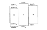
図2に、本発明の表示装置の一実施形態の青色素子の代表的なエネルギーバンド図を示す。図2に示されるように、この構成により青色発光層16Bに接してバンドギャップの大きい第2電子輸送層18を形成することにより、十分に電子が注入でき、ホールが発光層16Bから漏れることも防げるため、青色素子の発光効率を良くすることができる。
FIG. 2 shows a representative energy band diagram of a blue element of one embodiment of the display device of the present invention. As shown in FIG. 2, by forming the second
また、第1電子輸送層19のLUMO準位には電子が注入しやすいため、赤色発光層16Rに接してバンドギャップの狭い第1電子輸送層19を形成することにより、赤色素子の電圧を低くする事ができる。本発明では、第1電子輸送層19は異なる材料を積層して形成しても良く、この場合第2電子輸送層18と接して用いられる材料も式(A)の関係を満たす。
Further, since electrons are easily injected into the LUMO level of the first
また本発明では、青色発光層16Bのホスト材料と第2電子輸送層18のHOMO準位のエネルギーが下記式(B)の関係を満たすことが好ましい。
In the present invention, it is preferable that the energy of the HOMO level of the host material of the blue
HOMObh<HOMO2 (B) HOMO bh <HOMO 2 (B)
式(B)において、HOMObh、HOMO1はそれぞれ、青色発光層16Bのホスト材料、第2電子輸送層18のHOMO準位のエネルギーの絶対値を示す。
In the formula (B), HOMO bh and HOMO 1 represent the absolute values of the energy of the HOMO level of the host material of the blue
この場合、図2に示すように第2電子輸送層18のHOMO準位が青色発光層16Bのホスト材料のHOMO準位よりも深いため、ホールブロック層として働き、ホールが発光層16Bから漏れることをより防ぎ、青色素子の発光効率を更に良くすることができる。
In this case, as shown in FIG. 2, since the HOMO level of the second
また、青色発光層16Bは少なくともホスト材料と発光ドーパント材料を含み、青色発光層のホスト材料と発光ドーパント材料のHOMO準位のエネルギーとLUMO準位のエネルギーが下記式(C)の関係を満たすことがより好ましい。
The blue
LUMObh<LUMObd<HOMObh<HOMObd (C) LUMO bh <LUMO bd <HOMO bh <HOMO bd (C)
式(C)において、LUMObh、LUMObdはそれぞれ、青色発光層16Bのホスト材料、発光ドーパント材料のLUMO準位のエネルギーの絶対値を示す。また、HOMObh、HOMObdは青色発光層16Bのホスト材料、発光ドーパント材料のHOMO準位のエネルギーの絶対値を示す。
In the formula (C), LUMO bh and LUMO bd represent the absolute values of the LUMO level energy of the host material and the light emitting dopant material of the blue
この場合、図2に示されるように、青色発光層16Bは電子をトラップしやすくなるため、青色発光層16Bの主たる発光位置がより電子輸送層17側(第2電子輸送層18側)になり、ホールが発光層16Bから漏れることを抑制できる。よって、更に青色素子の発光効率を良くすることができる。さらに、式(B)を満たすことによりホールが青色発光層16Bから漏れることを抑制できる。
In this case, as shown in FIG. 2, since the blue
本発明において、第1電子輸送層19と第2電子輸送層18には従来から知られた電子輸送性材料を用いることができる。例としては、アルミニウムキノリノール錯体、ナフタレン化合物、アントラセン化合物、フェナントレン化合物、クリセン化合物、ピレン化合物、フルオランテン化合物、フェナントロリン化合物、アザ化合物などが挙げられる。
In the present invention, conventionally known electron transport materials can be used for the first
第1電子輸送層19の上には電子注入層20を形成してもよく、その上には光透過性を有する陰極21が形成される。
An
上記に述べた構成により、本発明は、パターニングマスクの着膜量及び洗浄頻度を最低限に抑え、赤色素子の電圧を上げずに青色素子の発光効率が高い有機EL表示装置を提供することができる。 With the above-described configuration, the present invention provides an organic EL display device in which the deposition amount of the patterning mask and the cleaning frequency are minimized, and the blue element has high luminous efficiency without increasing the voltage of the red element. it can.
尚、本発明で定義するバンドギャップは吸収スペクトルの吸収端から求めたものであり、HOMO及びLUMOは、エネルギーレベルの絶対値で示している。HOMOは大気中光電子分光法(AC−2)を用いて測定した。また、LUMOは、上記の方法で測定したHOMOの値から吸収スペクトルの吸収端から求めたバンドギャップを引いて算出した。 The band gap defined in the present invention is obtained from the absorption edge of the absorption spectrum, and HOMO and LUMO are shown as absolute values of energy levels. HOMO was measured using atmospheric photoelectron spectroscopy (AC-2). LUMO was calculated by subtracting the band gap obtained from the absorption edge of the absorption spectrum from the HOMO value measured by the above method.
以下、本発明の実施例について説明する。以下の実施例に用いた材料や素子構成は、特に好ましい例であるが、これに限定されるものではない。 Examples of the present invention will be described below. The materials and device configurations used in the following examples are particularly preferred examples, but are not limited thereto.
(実施例1、比較例2)
図1に示した断面構造の有機EL表示装置の青色素子を作製した。
(Example 1, Comparative Example 2)
A blue element of the organic EL display device having the cross-sectional structure shown in FIG. 1 was produced.
基板11としてガラスを用い、金属層13として銀(膜厚200nm)、透明導電層14としてIZO(膜厚20nm)を積層した陽極12が形成された電極付基板を形成し、UV/オゾン洗浄を施した。
Glass is used as the substrate 11, a substrate with an electrode on which an
続いて、真空蒸着装置(アルバック社製)に取り付け、1.33×10⁻⁴Pa(1×10⁻⁶Torr)まで排気した。その後、陽極12上にパターニングマスクを用いずにN,N’−α−ジナフチルベンジジンを20nm成膜し、正孔輸送層15を形成した。
Then, it attached to the vacuum evaporation system (made by ULVAC), and exhausted to 1.33 * 10 <-4> Pa (1 * 10 < -6 > Torr). Thereafter, an N, N′-α-dinaphthylbenzidine film having a thickness of 20 nm was formed on the
次に発光ドーパント材料として下記構造式(1)で示されるフルオランテン化合物(2質量%)、ホスト材料として下記構造式(2)で示されるピレン化合物を用い、厚さ20nmの青色発光層16Bを形成した。
Next, a fluoranthene compound (2% by mass) represented by the following structural formula (1) is used as the light-emitting dopant material, and a pyrene compound represented by the following structural formula (2) is used as the host material to form a blue light-emitting
次に、第2電子輸送層18として下記構造式(3)で示されるアザ化合物(バンドギャップ3.41eV)を10nmの膜厚で成膜した。さらに、第2電子輸送層18の上に、第1電子輸送層19として構造式(4)で示されるフェナントロリン化合物(バンドギャップ3.18eV)を10nmの膜厚で成膜した。
Next, an aza compound (band gap 3.41 eV) represented by the following structural formula (3) was formed to a thickness of 10 nm as the second
次に第1電子輸送層19上に炭酸セシウム(3容量%)と構造式(4)で表されるフェナントロリン化合物の共蒸着膜を40nmの膜厚で成膜し、電子注入層20とした。続いて、電子注入層20まで成膜した基板を、スパッタ装置(アルバック社製)へ真空中を搬送し、前記電子注入層20上にインジウム錫酸化物(IZO)をスパッタ法にて30nm成膜し、陰極21を形成した。その後、基板をグローブボックスに移し、窒素雰囲気中で乾燥剤を入れたガラスキャップにより封止した。
Next, a co-deposited film of cesium carbonate (3% by volume) and a phenanthroline compound represented by the structural formula (4) was formed to a thickness of 40 nm on the first

発光ドーパントとして用いた構造式(1)のフルオランテン化合物のLUMO準位のエネルギーは3.06eV、HOMO準位のエネルギーは5.85eVであった。また、ホスト材料として用いた構造式(2)のピレン化合物のLUMO準位のエネルギーは2.71eV、HOMO準位のエネルギーは5.70eVであった。 The LUMO level energy of the fluoranthene compound of the structural formula (1) used as the luminescent dopant was 3.06 eV, and the HOMO level energy was 5.85 eV. In addition, the LUMO level energy of the pyrene compound of the structural formula (2) used as the host material was 2.71 eV, and the HOMO level energy was 5.70 eV.
また、第2電子輸送層18として用いた構造式(3)のアザ化合物のLUMO準位のエネルギーは2.59eV、HOMO準位のエネルギーは6.00eVであった。第1電子輸送層19として用いた構造式(4)のフェナントロリン化合物のLUMO準位のエネルギーは2.65eV、HOMO準位は5.83eVであった。
The LUMO level energy of the aza compound represented by the structural formula (3) used as the second
従って、第1電子輸送層19と第2電子輸送層18のHOMO準位のエネルギーとLUMO準位のエネルギーの関係が、前記式(A)の関係を満たしていた。これにより後述の実施例2に記載する赤色発光層16Rに接してバンドギャップの狭い第1電子輸送層19を形成できるため、赤色素子の電圧を低くすることができた。
Therefore, the relationship between the energy of the HOMO level and the energy of the LUMO level of the first
また、第2電子輸送層18と青色発光層16Bのホスト材料は前記式(B)の関係を満たし、第2電子輸送層18はホールブロック層として働き、ホールが青色発光層16Bから漏れることをより防ぐことができた。
Further, the host materials of the second
さらに、青色発光層16Bは前記式(C)の関係を満たし、発光位置が電子輸送層17側であった。
Furthermore, the blue
また、比較例1として、電子輸送層17を構造式(4)で示されるフェナントロリン化合物のみで形成した以外は実施例1と同様に青色素子を作製した。
Further, as Comparative Example 1, a blue device was produced in the same manner as in Example 1 except that the
実施例1と比較例1の青色素子を比較したところ、比較例1の青色素子が電流効率3.4cd/Aに対し、実施例1の青色素子は4.0cd/Aと電流効率が高く、良好であった。 When the blue elements of Example 1 and Comparative Example 1 were compared, the blue element of Comparative Example 1 had a current efficiency of 3.4 cd / A, whereas the blue element of Example 1 had a high current efficiency of 4.0 cd / A. It was good.
(実施例2、比較例2)
青色発光層16Bの代わりに厚さ70nmの赤色発光層16Rを形成し、電子輸送層17(赤色素子は第1電子輸送層19のみである)を構造式(4)で示されるフェナントロリン化合物で形成した以外は実施例1と同様の方法で赤色素子を作製した。
(Example 2, comparative example 2)
Instead of the blue
赤色発光層16には、発光ドーパント材料として赤色発光することが知られたIr錯体(18容量%)、ホスト材料として4,4’−N,N’−ジカルバゾール−ビフェニルを用いた。
For the red
本例では、第1電子輸送層19をバンドギャップが狭い構造式(4)で示されるフェナントロリン化合物で形成したため、赤色素子の電圧を低くする事ができる。
In this example, since the first
また、比較例2として電子輸送層17を構造式(3)で示されるアザ化合物で形成した以外は実施例2と同様の方法で赤色素子を作製した。
Further, as Comparative Example 2, a red element was produced in the same manner as in Example 2 except that the
実施例2と比較例2の赤色素子を比較したところ、比較例2の赤色素子は20mA/cm2の電流を流した時の電圧が実施例2の赤色素子に比べて0.5V程度高かった。これは電子輸送層17として青色素子に適した電子輸送材料を用いたために電圧が高くなってしまったと考えられる。
When the red elements of Example 2 and Comparative Example 2 were compared, the voltage of the red element of Comparative Example 2 was about 0.5 V higher than the red element of Example 2 when a current of 20 mA / cm 2 was passed. . This is probably because the voltage was increased because an electron transport material suitable for a blue element was used as the
上記実施例1,2の手順により得られた青色及び赤色素子を用いることにより、発光層16以外でのパターニングマスクの使用回数が第2電子輸送層18の1回だけであるため、青色素子の発光効率が高く、赤色素子の駆動電圧の低い有機EL表示装置が提供される。
By using the blue and red elements obtained by the procedures of Examples 1 and 2 above, the patterning mask is used only once for the second
12:陽極、16:発光層、16R:赤色発光層、16G:緑色発光層、16B:青色発光層、17:電子輸送層、18:第2電子輸送層、19:第1電子輸送層、21:陰極 12: anode, 16: light emitting layer, 16R: red light emitting layer, 16G: green light emitting layer, 16B: blue light emitting layer, 17: electron transport layer, 18: second electron transport layer, 19: first electron transport layer, 21 :cathode
Claims (5)
前記各有機EL素子は、陰極と発光層の間に共通に配置されて、かつ、前記赤色を発する有機EL素子の発光層に接している第1電子輸送層を有し、
前記青色を発する有機EL素子は、前記第1電子輸送層と前記青色を発する有機EL素子の発光層との間に配置されて、前記青色を発する有機EL素子の発光層に接している第2電子輸送層を有し、
前記第2電子輸送層を形成する材料のバンドギャップが前記第1電子輸送層を形成する材料のバンドギャップよりも大きいことを特徴とする表示装置。 It has an organic EL element that emits red, an organic EL element that emits green, and an organic EL element that emits blue, and each organic EL element is between an anode, a cathode, and the anode and the cathode. A display device having a light emitting layer,
Each of the organic EL elements has a first electron transport layer that is disposed in common between the cathode and the light emitting layer and is in contact with the light emitting layer of the organic EL element that emits red light.
The organic EL element that emits blue light is disposed between the first electron transport layer and the light emitting layer of the organic EL element that emits blue, and is in contact with the light emitting layer of the organic EL element that emits blue light. Having an electron transport layer,
A display device, wherein a band gap of a material forming the second electron transport layer is larger than a band gap of a material forming the first electron transport layer.
LUMO2<LUMO1<HOMO1<HOMO2 (A)
(式(A)において、LUMO1、LUMO2はそれぞれ、前記第1電子輸送層、前記第2電子輸送層のLUMO準位のエネルギーの絶対値、HOMO1、HOMO2はそれぞれ、前記第1電子輸送層、前記第2電子輸送層のHOMO準位のエネルギーの絶対値を示す。) 2. The display device according to claim 1, wherein the energy of the HOMO level and the energy of the LUMO level of the first electron transport layer and the second electron transport layer satisfy the relationship of the following formula (A).
LUMO 2 <LUMO 1 <HOMO 1 <HOMO 2 (A)
(In Formula (A), LUMO 1 and LUMO 2 are the absolute values of the LUMO level energy of the first electron transport layer and the second electron transport layer, respectively, and HOMO 1 and HOMO 2 are the first electrons, respectively. (The absolute value of the energy of the HOMO level of the transport layer and the second electron transport layer is shown.)
HOMObh<HOMO2 (B)
(式(B)において、HOMObh、HOMO2はそれぞれ、前記ホスト材料、前記第2電子輸送層のHOMO準位のエネルギーの絶対値を示す。) The light emitting layer of the organic EL element emitting blue light contains a host material and a light emitting dopant material, and the energy of the HOMO level of the host material and the second electron transport layer satisfies the relationship of the following formula (B): The display device according to claim 1 or 2.
HOMO bh <HOMO 2 (B)
(In Formula (B), HOMO bh and HOMO 2 represent the absolute values of the HOMO level energies of the host material and the second electron transport layer, respectively.)
LUMObh<LUMObd<HOMObh<HOMObd (C)
(式(C)において、LUMObh、LUMObdはそれぞれ、前記ホスト材料、前記発光ドーパント材料のLUMO準位のエネルギーの絶対値、HOMObh、HOMObdはそれぞれ、前記ホスト材料、前記発光ドーパント材料のHOMO準位のエネルギーの絶対値を示す。) The light emitting layer of the organic EL element emitting blue light includes a host material and a light emitting dopant material, and the energy of the HOMO level and the energy of the LUMO level of the host material and the light emitting dopant material satisfy the relationship of the following formula (C). The display device according to claim 1, wherein the display device is a display device.
LUMO bh <LUMO bd <HOMO bh <HOMO bd (C)
(In Formula (C), LUMO bh and LUMO bd are the absolute values of the LUMO level energy of the host material and the light-emitting dopant material, respectively, and HOMO bh and HOMO bd are the host material and the light-emitting dopant material, respectively. (The absolute value of the energy of the HOMO level is shown.)
Priority Applications (1)
| Application Number | Priority Date | Filing Date | Title |
|---|---|---|---|
| JP2011002692A JP2012146764A (en) | 2011-01-11 | 2011-01-11 | Display device |
Applications Claiming Priority (1)
| Application Number | Priority Date | Filing Date | Title |
|---|---|---|---|
| JP2011002692A JP2012146764A (en) | 2011-01-11 | 2011-01-11 | Display device |
Publications (1)
| Publication Number | Publication Date |
|---|---|
| JP2012146764A true JP2012146764A (en) | 2012-08-02 |
Family
ID=46790060
Family Applications (1)
| Application Number | Title | Priority Date | Filing Date |
|---|---|---|---|
| JP2011002692A Withdrawn JP2012146764A (en) | 2011-01-11 | 2011-01-11 | Display device |
Country Status (1)
| Country | Link |
|---|---|
| JP (1) | JP2012146764A (en) |
Cited By (10)
| Publication number | Priority date | Publication date | Assignee | Title |
|---|---|---|---|---|
| JP2015032582A (en) * | 2013-07-31 | 2015-02-16 | エルジー ディスプレイ カンパニー リミテッド | White organic electroluminescent element |
| KR20150059715A (en) * | 2013-11-22 | 2015-06-02 | 엘지디스플레이 주식회사 | Organic light emitting diode display device and fabricating method thereof |
| KR20170115642A (en) * | 2016-04-07 | 2017-10-18 | 삼성디스플레이 주식회사 | Organic light emitting device |
| US9893124B2 (en) | 2014-04-30 | 2018-02-13 | Samsung Display Co., Ltd. | Organic light-emitting display |
| JP2020035942A (en) * | 2018-08-31 | 2020-03-05 | 三国電子有限会社 | Organic electroluminescence element having carrier injection amount control electrode |
| WO2021214910A1 (en) * | 2020-04-22 | 2021-10-28 | シャープ株式会社 | Light-emitting element and display device |
| US11476450B2 (en) | 2019-02-22 | 2022-10-18 | Mikuni Electron Corporation | Display device |
| US11626463B2 (en) | 2017-05-31 | 2023-04-11 | Mikuni Electron Corporation | Display device and method for manufacturing the same |
| US11630360B2 (en) | 2020-02-05 | 2023-04-18 | Mikuni Electron Corporation | Liquid crystal display device |
| US11929439B2 (en) | 2018-09-26 | 2024-03-12 | Mikuni Electron Corporation | Transistor, method of manufacturing transistor, and display device using the same |
-
2011
- 2011-01-11 JP JP2011002692A patent/JP2012146764A/en not_active Withdrawn
Cited By (17)
| Publication number | Priority date | Publication date | Assignee | Title |
|---|---|---|---|---|
| US9281487B2 (en) | 2013-07-31 | 2016-03-08 | Lg Display Co., Ltd. | White organic light emitting diode device |
| JP2015032582A (en) * | 2013-07-31 | 2015-02-16 | エルジー ディスプレイ カンパニー リミテッド | White organic electroluminescent element |
| KR20150059715A (en) * | 2013-11-22 | 2015-06-02 | 엘지디스플레이 주식회사 | Organic light emitting diode display device and fabricating method thereof |
| KR102249192B1 (en) * | 2013-11-22 | 2021-05-10 | 엘지디스플레이 주식회사 | Organic light emitting diode display device and fabricating method thereof |
| US9893124B2 (en) | 2014-04-30 | 2018-02-13 | Samsung Display Co., Ltd. | Organic light-emitting display |
| KR20170115642A (en) * | 2016-04-07 | 2017-10-18 | 삼성디스플레이 주식회사 | Organic light emitting device |
| CN107275496A (en) * | 2016-04-07 | 2017-10-20 | 三星显示有限公司 | Organic luminescent device |
| KR102642199B1 (en) * | 2016-04-07 | 2024-03-05 | 삼성디스플레이 주식회사 | Organic light emitting device |
| US11678498B2 (en) | 2016-04-07 | 2023-06-13 | Samsung Display Co., Ltd. | Organic light-emitting device |
| US11626463B2 (en) | 2017-05-31 | 2023-04-11 | Mikuni Electron Corporation | Display device and method for manufacturing the same |
| US11937458B2 (en) | 2017-05-31 | 2024-03-19 | Mikuni Electron Corporation | Display device and method for manufacturing the same |
| JP2020035942A (en) * | 2018-08-31 | 2020-03-05 | 三国電子有限会社 | Organic electroluminescence element having carrier injection amount control electrode |
| JP7190729B2 (en) | 2018-08-31 | 2022-12-16 | 三国電子有限会社 | ORGANIC ELECTROLUMINESCENT DEVICE HAVING CARRIER INJECTION CONTROL ELECTRODE |
| US11929439B2 (en) | 2018-09-26 | 2024-03-12 | Mikuni Electron Corporation | Transistor, method of manufacturing transistor, and display device using the same |
| US11476450B2 (en) | 2019-02-22 | 2022-10-18 | Mikuni Electron Corporation | Display device |
| US11630360B2 (en) | 2020-02-05 | 2023-04-18 | Mikuni Electron Corporation | Liquid crystal display device |
| WO2021214910A1 (en) * | 2020-04-22 | 2021-10-28 | シャープ株式会社 | Light-emitting element and display device |
Similar Documents
| Publication | Publication Date | Title |
|---|---|---|
| JP2012146764A (en) | Display device | |
| US9088001B2 (en) | Organic light emitting display and method for fabricating the same | |
| JP4898560B2 (en) | Organic light emitting device | |
| JP5975831B2 (en) | Display device | |
| US9076978B2 (en) | Organic light emitting diode device | |
| JP6387566B2 (en) | Organic EL device | |
| US9136309B2 (en) | Organic electroluminescent display | |
| US8183564B2 (en) | Multicolor display apparatus | |
| JP6060361B2 (en) | Organic light emitting device | |
| JP6340616B2 (en) | Organic EL element and organic EL display panel | |
| US8063558B2 (en) | Multi-color display apparatus | |
| JP6815294B2 (en) | Organic EL element and organic EL panel | |
| WO2020194411A1 (en) | Light-emitting element and light-emitting device | |
| JP2008130485A (en) | Organic electroluminescent device array | |
| JP5783853B2 (en) | Display device | |
| JP2008084910A (en) | Organic el display | |
| KR20160035561A (en) | Organic Light Emitting Device | |
| JP5854706B2 (en) | Display device | |
| WO2015190550A1 (en) | Organic element | |
| WO2015182130A1 (en) | Organic el element and organic el light-emitting device | |
| JP2013051161A (en) | Display device | |
| TWI569492B (en) | Organic light-emitting element | |
| US10476022B2 (en) | Organic light emitting diode and manufacturing method thereof, display apparatus | |
| JP2004119086A (en) | Display | |
| JP2013051159A (en) | Display device |
Legal Events
| Date | Code | Title | Description |
|---|---|---|---|
| A300 | Application deemed to be withdrawn because no request for examination was validly filed |
Free format text: JAPANESE INTERMEDIATE CODE: A300 Effective date: 20140401 |