EP2833378A1 - Transformer - Google Patents
Transformer Download PDFInfo
- Publication number
- EP2833378A1 EP2833378A1 EP13178808.5A EP13178808A EP2833378A1 EP 2833378 A1 EP2833378 A1 EP 2833378A1 EP 13178808 A EP13178808 A EP 13178808A EP 2833378 A1 EP2833378 A1 EP 2833378A1
- Authority
- EP
- European Patent Office
- Prior art keywords
- transformer
- insulating element
- cooling
- insulating
- periphery
- Prior art date
- Legal status (The legal status is an assumption and is not a legal conclusion. Google has not performed a legal analysis and makes no representation as to the accuracy of the status listed.)
- Granted
Links
Images


Classifications
-
- H—ELECTRICITY
- H01—ELECTRIC ELEMENTS
- H01F—MAGNETS; INDUCTANCES; TRANSFORMERS; SELECTION OF MATERIALS FOR THEIR MAGNETIC PROPERTIES
- H01F27/00—Details of transformers or inductances, in general
- H01F27/08—Cooling; Ventilating
-
- H—ELECTRICITY
- H01—ELECTRIC ELEMENTS
- H01F—MAGNETS; INDUCTANCES; TRANSFORMERS; SELECTION OF MATERIALS FOR THEIR MAGNETIC PROPERTIES
- H01F27/00—Details of transformers or inductances, in general
- H01F27/34—Special means for preventing or reducing unwanted electric or magnetic effects, e.g. no-load losses, reactive currents, harmonics, oscillations, leakage fields
- H01F27/36—Electric or magnetic shields or screens
- H01F27/363—Electric or magnetic shields or screens made of electrically conductive material
-
- H—ELECTRICITY
- H01—ELECTRIC ELEMENTS
- H01F—MAGNETS; INDUCTANCES; TRANSFORMERS; SELECTION OF MATERIALS FOR THEIR MAGNETIC PROPERTIES
- H01F27/00—Details of transformers or inductances, in general
- H01F27/08—Cooling; Ventilating
- H01F27/10—Liquid cooling
-
- H—ELECTRICITY
- H01—ELECTRIC ELEMENTS
- H01F—MAGNETS; INDUCTANCES; TRANSFORMERS; SELECTION OF MATERIALS FOR THEIR MAGNETIC PROPERTIES
- H01F27/00—Details of transformers or inductances, in general
- H01F27/28—Coils; Windings; Conductive connections
- H01F27/288—Shielding
- H01F27/2885—Shielding with shields or electrodes
-
- H—ELECTRICITY
- H01—ELECTRIC ELEMENTS
- H01F—MAGNETS; INDUCTANCES; TRANSFORMERS; SELECTION OF MATERIALS FOR THEIR MAGNETIC PROPERTIES
- H01F27/00—Details of transformers or inductances, in general
- H01F27/28—Coils; Windings; Conductive connections
- H01F27/32—Insulating of coils, windings, or parts thereof
-
- H—ELECTRICITY
- H01—ELECTRIC ELEMENTS
- H01F—MAGNETS; INDUCTANCES; TRANSFORMERS; SELECTION OF MATERIALS FOR THEIR MAGNETIC PROPERTIES
- H01F27/00—Details of transformers or inductances, in general
- H01F27/34—Special means for preventing or reducing unwanted electric or magnetic effects, e.g. no-load losses, reactive currents, harmonics, oscillations, leakage fields
- H01F27/36—Electric or magnetic shields or screens
Definitions
- the invention relates to the field of power electronics, such as an induction electric apparatus, in particular a transformer.
- An induction electric apparatus such as a transformer is part of a general power network system, in particular for transmitting power from a power plant to consumers.
- the transformer may be located in an environment where space is limited.
- the transformer needs to be designed to fit the limited space.
- An issue arising from said limited space is an required insulation between a primary and a secondary winding of the transformer starting to dominate the transformer size at high frequencies and/or small power. This issue may be resolved by filling the transformer, i.e. its enclosure, with a solid insulating material such as silicone.
- the power density of the transformer needs to be increased to put large amounts of power through said apparatus.
- the power density of the transformer is generally limited by a maximum operating temperature.
- the maximum operating temperature depends on ambient temperature, energy losses during operation of the apparatus, and a thermal energy transfer of a region from an internal hot spot region.
- By filling the transformer with a solid insulating material the heat transfer away from said hot spots within the transformer is limited. Therefore, improving the heat transfer through the transformer components is critical to reduce volume as well as weight of the transformer and its components.
- the operating frequency can only be increased up to a maximum operating frequency due to several limiting factors such as an increasing operating temperature with increased frequency-dependent losses and reduced transformer size, required frequency-independent minimum insulation distances, or minimum insulation distances between the primary and the secondary winding.
- the minimum distances between the primary and secondary winding is determining the size of the transformer if its size is reduced by employing high frequencies.
- the increasing loss density and the maximum operating temperature require improved cooling of the transformer.
- Document GB 853,913 describes a transformer, including a high-voltage layer winding, having one or more stress-distributing shields arranged between winding layers which are parallel connected. Electrically conductive shields are provided between the layers and are connected to the start and finish of the winding respectively. Electrostatic rings are provided in which the space between the layers forms a cooling duct.
- the optional cooling ducts in the prior art are located in the electric field between the shields, and the electric field will concentrate in said cooling ducts. This effect is intensified for a solid insulation between the windings for instance silicone gel. This will result in partial discharge within the cooling ducts leading to damage of the insulation of the transformer.
- a transformer is at least comprising a core, a primary winding, i.e. a coil, a secondary winding, at least one cooling channel, i.e. a pipe or duct, and an enclosure such as a casing, shell, or hull.
- the enclosure accommodates, i.e. receives or contains, the core, the cooling channel, and the primary winding and the secondary winding for instance such that the primary winding and the secondary winding are entirely enclosed, i.e. received or contained, by the enclosure.
- the enclosure is further filled with an electrically insulating medium or agent, i.e.
- the cooling channel provides cooling for the primary and secondary winding, the core, the insulating medium, and the enclosure.
- an insulating element for instance a solid insulating element, i.e. a core, base, or kernel, is placed between the primary winding and the secondary winding.
- the insulating element may be suited to receive a large electric field for instance due to a potential difference, i.e. voltage difference, between the primary and secondary winding.
- a first conducting shield i.e. an element, unit, screen, or buffer is placed between the insulating element and the primary winding and a second conducting shield is placed between the insulating element and the secondary winding.
- the first conducting shield is electrically connected to the primary winding and the second conducting shield is electrically connected to the secondary winding. This way the potential between the primary and secondary winding is transferred to the first and second conducting shield such that the electric field is confined in or limited to the insulating element.
- the first cooling channel is placed between the first conducting shield and the primary winding.
- the cooling channel may therefore be in direct contact with the insulating medium.
- the first cooling channel may transfer heat produced in the transformer, e.g. by the primary and secondary windings, to the outside of the transformer for instance the cooling channel may be part of a larger cooling system.
- the periphery of the conducting shield gives rise to two major issues to be considered, first an increased or enhanced surface electric field from the conducting shield along an interface with the insulating element leading to surface and corona discharges with a risk for flashover breakdown, i.e. a voltage breakdown along the surface; and second an increased or enhanced electric field penetrating into the insulating element leading to heightened stress and discharges in the insulating element and eventually to dielectric breakdown.
- the periphery, i.e. border or boundary, of the first and the second conducting shield is drawn-in, i.e. retracted or recessed with respect to a periphery of the insulating element and wherein one of the first or second conducting shields is drawn-in further than the other conducting shield.
- the conducting shield may be drawn-in on one side for roughly the width, i.e. thickness, of the insulating element, wherein the other conducting shield on the opposite side of the insulating element is drawn-in twice or more the width, i.e. thickness, of the insulating element.
- This way an easy to build design is provided to reduce the stress on the periphery of the conducting shield.
- a further insulating element may be placed on the periphery of the insulating element covering the periphery of the conducting shields.
- a further embodiment of the invention includes a nonlinear resistive field grader or a field grading material placed between at least one of the first or second conducting shields.
- the field grader is drawn-in with respect to the periphery of the insulating element and is drawn-in less than said conducting shield in the periphery. i.e. covers a greater area than the conducting shield.
- surface and bulk electric fields are effectively reduced.
- the nonlinear material of the field grader must have the correct switching field strength, which is the electric field strength at which the material switches from the insulating to the conductive mode.
- the switching field strength must be in the order of the ratio between maximum voltage applied and length or area of the field grading layer on the insulating element.
- the width, i.e. thickness, of the insulating element may be significantly reduced compared to the design without the field grader.
- the conducting shield on one side may be placed on top of the field grader and its periphery may be drawn-in about twice as much a periphery of the field grader with respect to the periphery of the insulating element.
- the second conducting shield may be drawn-in less than the width, i.e. thickness, of the insulating element.
- a further insulating element may be placed on the periphery of the insulating element covering the periphery of the conducting shields.
- nonlinear resistive field grading layer is mixing ZnO microvaristor for instance in a polymer matrix.
- ZnO microvaristor electrical characteristics can be widely tailored by specific doping and processing, e.g. the switching field strength ranging from 50V/mm up to 5000V/mm, and high nonlinearity is achieved with ZnO microvaristors.
- the nonlinearity is important since the higher the nonlinearity coefficient of the material, the better is its field grading performance, i.e., the lower a leakage current, and the less its frequency dependence.
- Other material or fillers for nonlinear resistive field grading may be SiC, doped SnO 2 or carbon black.
- other field grading methods such as linear resistive field control or refractive field grading may be considered.
- a periphery of at least one of the first and second conducting shields is curved away from the insulating element and wherein the insulating element has an enlarged periphery section, i.e. T-section or T-shaped periphery, supporting the curved periphery of said conducting shield.
- This way geometric field control via curved shields is provided. This is an effective field control to lower bulk and surface electric fields.
- a further insulating element may be placed on the periphery of the insulating element covering the periphery of the conducting shields. The distance from the periphery of the first and second conducting shields is around the width, i.e.
- the width, i.e. thickness, of the insulating element at least in the center of the insulating element may be significantly reduced compared to the design without the curved conducting shields.
- the transformer is a medium frequency transformer, wherein the primary winding and the secondary winding are formed of Litz wire and/or foil winding and wherein further the primary winding and the secondary winding are placed on the core forming a gap between the primary winding and the secondary winding.
- the cooling channel and/or the core are in direct contact with the insulating medium.
- no gap i.e. an air gap
- heat transfer from the insulating medium to the cooling channel and the core is improved through the direct contact.
- the direct contact between the insulating medium and the cooling channel and the core may be particularly relevant for a medium frequency transformer, where high voltages may cause partial discharges and high frequencies may cause high amounts of heat.
- the cooling channels are part of a circulation system, e.g. comprising a pump and further supply and drain channels, provided with a cooling medium, i.e. liquid or gas, flowing through the cooling channel.
- a cooling medium i.e. liquid or gas
- the transformer may be actively cooled.
- a more dense cooling liquid may be used.
- the circulation system such as the pump may be a less sophisticated device for instance for air no tight sealing may be necessary.
- a second cooling channel is placed between the second conducting shield and the secondary winding. This way the cooling properties may be further improved and more heat may be transferred away from the hot spots of the primary and secondary windings. This may be necessary for applications causing a large amount of heat in the transformer. For other applications the transformer may be implemented more simple with only the first cooling channel.
- a cooling element such as cooling plates, e.g. heat sink, cold plate, or two-phase cooling, is placed on the core, the insulating element, the insulating medium, and/or the enclosure for cooling of the transformer.
- the cooling element may provide a further way of transporting heat away from hot spots in the transformer and may be combined with the cooling channels and the circulation system.
- the insulating medium is one of a silicone gel, transformer oil, silicone-based or fluorinated hydrocarbons, polyurethane, synthetic rubber, any mix of these materials or any other similar material suited for cooling.
- a suited material may be for instance stable or suited for a temperature ranging between -40°C and +150°C and may have further a dielectric breakdown strength for instance from 15 to 22kV/mm. However, different parameters may apply for some applications.
- the insulating medium is a liquid and filled in the enclosure for instance from a top side of the enclosure.
- the enclosure provides additional space for expansion of the insulating medium due to cycling and aging of the insulating medium within the enclosure.
- Silicone Gel used for power electronic modules is specified generally for temperature ranges between -40° and +150°C, i.e. for usage in 6.5kV power electronics modules with an expected 25 years of lifetime.
- Dielectric breakdown strength is typically 15 - 22kV/mm. Breakdown strength itself is not dependent on aging as the chemical structure is not changed, it is much more dependent on filling quality, voids and moisture uptake and partial discharge which depend mainly on processing and operation conditions.
- the enclosure containing the silicone gel is filled from the top side with space provided for material expansion and contractions due to cycling and aging. This way the lifetime of the insulating medium may be improved.
- the transformer may be a single-phase, three-phase, or multi-phase transformer, i.e. a shell-type or core-type transformer.
- a cross-section of the insulating medium in an opening, i.e. a winding window or cut, of the core is greater than the cross-section of the primary winding and the secondary winding in said winding window, i.e. a copper-filling-factor of a winding window of the core is below 50%.
- the invention improves the cooling of the transformer, thus, the power density of said transformer may be increased or at a given power and insulation voltage the transformer may be designed with a reduced weight and with reduced size compared to the prior art.
- the invention further provides a significant cost-, weight- and volume-reduction for a transformer in particular for a medium frequency transformer, especially if there are high voltages between primary- and secondary winding. Further yet a simple and effective cooling of the windings via convection very close to the windings and significantly reduced reliability problems associated with partial discharge in solid insulation materials and/or the cooling system are provided by the invention.
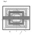
- Fig.1 schematically shows a cross-section of a transformer 1 along horizontal plane of the transformer.
- the transformer i.e. medium frequency transformer of a shell-type, at least comprising a core 2, a primary winding 3, a secondary winding 4, at least one cooling channel 5, and an enclosure 6.
- the windings 3, 4 may be formed from Litz wire and/or foil winding, in particular for a medium frequency transformer.
- the enclosure 6 accommodates the core 2, the primary winding 3 and the secondary winding 4 such that the primary winding 3 and the secondary winding 4 is entirely enclosed by the enclosure 6. Further the enclosure 6 is filled with an insulating medium 7 enabling heat transfer from the primary winding 3 and the secondary winding 4 to the cooling channel 5.
- an insulating element 8 is placed as dielectric barrier.
- the insulating element 8 fully surrounds the secondary winding 4, where the primary winding 3 surrounds the insulating element 8.
- insulating shields 9 and 10 are placed on the insulating element 8.
- Said conducting shields 9 and 10 are ring shaped as well. Further said conducting shields 9 and 10 are electrically connected to the primary winding 3 and the secondary winding 4 respectively such that the conducting shield 9 is at the same potential as the primary winding 3 and the conducting shield 10 is at the same potential as the secondary winding 4.
- the insulating medium 7 may be in direct contact with the cooling channel 5 and the primary and secondary winding 3 and 4.
- the insulating medium also serves as a heat conductor to transfer heat away from hot spots in the transformer 1, i.e. the primary and secondary winding 3 and 4.
- By directly contacting the insulating medium 7 with the cooling channel 5 and the primary and secondary winding 3 and 4 it is ensured that heat is properly conducted away from the hot spot and transferred away from the transformer 1 by the cooling channel 5.
- a second cooling channel 15 may be placed on the opposite side of the insulating element 8, i.e. facing the secondary winding 4. This way an improved heat transport away from the secondary winding 4 is enabled.
- the cooling channels 5 and 15 may be implemented as pipes or ducts, or as shown in Fig.1 as a plurality of pipes.
- the plurality of the pipes allows to increase the surface area which is cooled, and allows to adjust the pressure drop in the pipes for optimizing the coolant flow.
- any cooling liquid may be used to be pumped through the cooling channels 5 and 15.
- An alternative would be the use of air ducts in the insulating medium 7 as cooling channels 5 and 15.
- the insulating medium 7 may have gaps extending through the transformer 1. This may be a simple way of providing cooling channels 5 and 15 by forcing for instance air or any other suitable cooling gas through said gaps. This simple cooling option may be suitable for some applications with less heat production in the transformer 1.
- cooling channels 5 and 15 may surround or may be surrounded by the insulating element 8 along all sides. This may be balanced by the ratio of necessary insulation between the primary and secondary winding 3 and 4 and the necessary cooling provided by the cooling channels 5 and 15.
- the volume of the cooling channels 5 and 15 may be reduced by confining the cooling channels 5 and 15 to only one or two main sides of the insulating element 8 or by reducing its width over one side of the insulating element 8 as shown in Fig. 1 .
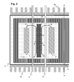
- Fig. 2 schematically shows a view as marked by the arrow along the section II-II of the shell-type transformer 1 of Figure 1 with the insulating element 8, the cooling channels 5 and 15 and in addition to what is shown in Figure 1 with cooling elements 19.
- the view of the transformer 1 is however for simplicity shown only partly in Fig. 2 , where the shell-type transformer 1 is symmetrical and the shown features are to be mirrored on the right side of the core 2.
- the conducting shields 9 and 10 are placed on the insulating element 8 symmetrically, i.e. on one side facing the primary winding 3 and on another side facing the secondary winding 4.
- the insulating element 8 and the conducting shields 9 and 10 are ring shaped and surround the central leg of the transformer core 2.
- the conducting shields 9 and 10 are further drawn-in direction of the axis A and with respect to a periphery 11, 21 of the conducting shield respectively and to a periphery 12 of the insulating element 8.
- the axis A is defining the vertical direction of the transformer 1.
- the conducting shields 9 and 10 are of reduced length in direction of axis A in respect of the extension of the insulating element 8 in the direction of axis A. This way peak fields on the periphery 12 of the insulating element 8 are avoided and the lifetime of the insulating element 8 is increased.
- the conducting shields 9 and 10 are electrically connected to the primary and secondary windings 3 and 4.
- an electrical connection 17 connects the primary winding 3 with the conducting shield 9
- an electrical connection 18 connects the secondary winding 4 with the conducting shield 10.
- the conducting shield 9 is on the same electrical potential as the primary winding 3
- the conducting shield 10 is on the same electrical potential as the secondary winding 4 .
- the electric field caused by the potential difference of the primary and secondary winding 3 and 4 is then confined between the conducting shields 9 and 10, where the insulating element 8 is made of a suitable material to further confine the electric field only to the insulating element 8.
- the insulating medium 7 is in direct contact with the conducting shields 9 and 10, the insulating element 8, the cooling channels 5 and 15, the primary and secondary windings 3 and 4, the core 2, and with the enclosure 6 in order to avoid any gaps, i.e. air gaps between the components which may lead to partial discharges and damage to the transformer 1. This way the invention avoids partial discharges and damage to any parts of the transformer 1 and further prolonging the lifetime of the transformer 1.
- the core 2 may be employed as a cooling element by serving as a heat sink which may be additionally cooled by the cooling channels 5 and 15.
- an cooling element 19 such as cooling plates, e.g. a heat sink, cold plate, or a two -phase cooling maybe placed on the core 2, the insulating element 8, the insulating medium 7, and/or the enclosure 6 for cooling of the transformer 1.
- the cooling element 19 on the top and the bottom side of the enclosure 6 as shown in Fig. 2 is a heat sink with fins and a base, where the fins are increasing a surface area of the heat sink to increase the amount of dissipated heat via the heat sink to ambient.
- cooling element 19 may be more sophisticated and require a cooling system with a cooling liquid, ducts, and a pump. Such a sophisticated cooling system may be necessary in some applications where large amounts of heat need to be dissipated from the transformer 1
- the cooling element 19 may be placed for instance on the core 2 or be in direct contact with the insulating medium 7.
- the cooling channels 5 and 15 may be part of a larger cooling system as well. In this case a cooling liquid is forced through the cooling channels 5 and 15.
- the cooling liquid may be a liquid or gas, where a more dense liquid may provide better heat transport and thus better cooling of the transformer 1.
- tight sealing of supply and drain ducts connected to the cooling channels 5 and 15 may be necessary so that no cooling liquid spills.
- a pump may be necessary to force the cooling liquid through the cooling channels 5 and 15 and the supply drain ducts respectively.
- the insulating medium 7 may be one of a silicone gel, transformer oil, silicone-based or fluorinated hydrocarbons, polyurethane, synthetic rubber.
- a thermal conductivity of silicone gel can be higher than 20 times the thermal conductivity of air.
- the thermal conductivity may be about a factor 8 higher.
- epoxy filling has a thermal conductivity comparable to silicone gel, but as a solid material, serious reliability problems may occur such as cracks due to thermal cycling, partial discharge in cracks and voids.
- epoxy filling may also be a suitable insulating medium 7.
- An advantage of silicone gel over other material is its high breakthrough field strength which allows insulation distances within the transformer 1, especially between windings 3, 4 and core 2, to be reduced by about a factor three or more compared to air insulation.
- the invention allows reducing size and further simplifying the cooling of a transformer 1.
- the heat i.e. thermal losses, flows from the windings 3, 4 via thermal conduction through the insulating medium 7 to the cooling channels 5 and 15.
- This configuration not only allows shrinking the component size significantly but also allows improved cooling.
- the copper cross section of the windings 3, 4 fills less than 50% of the winding window of the core 2.
- the insulating medium 7 may be supplied initially as two liquid components for mixing.
- the two components start cross linking after mixing.
- the mixture of the two liquid components is further cured.
- other material may be supplied as a granulate which is filled in the enclosure 6 and is further distributed or melted in the enclosure 6, i.e. by applying heat for a specified period of time. This may be carried out while placing the enclosure 6 for instance on a table where the granulate or the melted insulating material 7 may not leak or may only get in contact with the table top. After a cooling period the insulating material 7 solidifies and tight sealing of the enclosure is not necessary. Any material on the outside of the enclosure that may have leaked can be removed easily after solidification. However, proper outgassing of the material is necessary
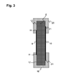
- Fig. 3 shows a cross-section of another embodiment of the insulating element 8 with the conducting shields 9 and 10 as it may be implemented in the transformer 1 of Figure 1 and 2 , where the conducting shields 9, 10 are placed on the insulating element 8 such that stress on the periphery 11 and 21 of the conducting shields 9 and 10 may be controlled.
- the periphery 11, 21 of the conducting shields 9 and 10 give rise to two major issues to be considered. At first a surface electric field of the surface of the conducting shields 9 and 10 along an interface with the insulating element 8 may be increased and thus leading to surface and corona discharges with a risk for flashover breakdown, i.e. a voltage breakdown along the surface. At second an electric field penetrating into the insulating element 8 may be increased and thus leading to heightened stress and discharges in the insulating element 8 and eventually to dielectric breakdown.
- FIG. 3 shows the periphery 11 and 21 of the conducting shields 9 and 10 drawn-in or recessed with respect to the periphery 12 of the insulating element 8. This way peak electric fields on the periphery 12 of the insulating element 8 are avoided and this results in a longer lifetime of the insulating element 8.
- the periphery 11 of the conducting shield 9 in Figure 3 is drawn-in more than the periphery 21 of the conducting shield 10. Thus, resulting in a slight asymmetric placement of the conducting shields 9 and 10 on the insulating element 8. This way peak electric fields are further reduced.
- a insulating cover element 16 may be placed on one end of the insulating element 8 for further protection of the periphery 11, 21 of the conducting shields 9 and 10 and the periphery 12 of the insulating element 8.
- the s insulating cover element 16 is covering the periphery 11 and 21 of the conducting shields and may have a U-shaped cross-section.
- another insulating cover element 20 is placed on the opposite side of the insulating cover element 16 on the insulating element 8 to cover both ends of the insulating element 8.
- Fig 4 shows a cross-section of an insulating element 8 as shown in Figure 3 and having in addition a nonlinear resistive field grader 14 placed in between the insulating element 8 and the conducting shield 9.
- the field grader 14 covers an area greater than the conducting shield 9 and has therewith an larger extension in the vertical direction of the transformer 1 compared to the extension of the conducting shield 9 in this direction.
- the field grader 14 reduces surface and bulk electric fields effectively. At the transition of an electric field from one medium to another medium, electric stresses harmful to the electric equipment can ensue due to a discontinuity in the electric field.
- Field grading or field grading material is causing the capacitance and electric stress to be more uniformly distributed between the conducting shield 9 and the insulating element 8. The application of such a field grading material as a field grader 14 results for instance in an increase of the breakdown voltage.
- the nonlinear material of the field grader 14 must be designed to have the correct switching field strength which is the electric field strength at which the material switches from the insulating to the conductive mode.
- the switching field strength must be in the order of the ratio between maximum voltage applied and length of or area covered by the field grader 14, i.e. field grading layer.
- a preferred design of the nonlinear resistive field grading layer is mixing ZnO microvaristor into a polymer matrix.
- ZnO microvaristor electrical characteristics can be widely tailored by specific doping and processing where the electric field strength ranges from 50V/mm up to 5000V/mm and high nonlinearity is achieved with ZnO microvaristors. The latter is important since the higher the nonlinearity coefficient of the material, the better is its field grading performance, i.e., the lower the leakage current, and the less its frequency dependence.
- Other material or fillers for nonlinear resistive field grading are SiC, doped SnO2 or carbon black.
- Other field grading methods such as linear resistive field control or refractive field grading may be applied as well.
- an insulating cover element 16 may be placed on one end of the insulating element 8 for further protection of the periphery 11, 21 of the conducting shields 9 and 10 and the periphery 12 of the insulating element 8 as described with respect to Fig. 3 .
- Fig. 5 shows another embodiment of the insulating element 8 as shown in the Figures 3 and 4 and as it may implemented in the transformer 1 shown in the figures 1 and 2 .
- the insulating element 8 of Figure 5 having the periphery 12 being curved and having the periphery 11, 21 of the conducting shields 9 and 10 being curved. This is an effective field control to lower bulk and surface electric fields.
- the periphery 12 of the insulating element 8 is curved as to support the curved periphery 11, 21 of the conducting shields 9 and 10.
- the insulating element 8 has a width or thickness depending on the actual embodiment.
- the embodiment according to Fig. 3 has the greatest thickness and requires the most material, where the embodiments according to Fig. 4 and Fig. 5 have a similar thickness at least in the center of the insulating element 8.
- the embodiment of Fig. 4 is more complex and costly to actually form but does not require any field grading material such as the field grader 14.
- the use of one or another embodiment may depend on the actual application of the transformer 1 and the electric field and stress present in the insulating element 8.
- insulating medium 7 i.e. for a Silicon gel based transformer 1 according to the invention with a conventional air-insulated transformer
- medium frequency transformers are considered employing copper-litz wire and a Ferrite N87 magnetic core 2 for a power of 170 kVA, an operating frequency of 3.5 kHz, and a voltage insulation between primary and secondary winding of 50kV.
- the transformer 1 according to the invention allows a reduction of the transformer volume by more than 2/3 compared to transformer of the prior art employing the same ratings.
- the mass of windings 3, 4 plus core 2 is reduced by more than half compared to air insulation combined with convective air cooling.
Landscapes
- Engineering & Computer Science (AREA)
- Power Engineering (AREA)
- Regulation Of General Use Transformers (AREA)
Abstract
Description
- The invention relates to the field of power electronics, such as an induction electric apparatus, in particular a transformer.
- An induction electric apparatus such as a transformer is part of a general power network system, in particular for transmitting power from a power plant to consumers. However, the transformer may be located in an environment where space is limited. Thus, the transformer needs to be designed to fit the limited space. An issue arising from said limited space is an required insulation between a primary and a secondary winding of the transformer starting to dominate the transformer size at high frequencies and/or small power. This issue may be resolved by filling the transformer, i.e. its enclosure, with a solid insulating material such as silicone.
- At the same time a power density of the transformer needs to be increased to put large amounts of power through said apparatus. However, the power density of the transformer is generally limited by a maximum operating temperature. The maximum operating temperature depends on ambient temperature, energy losses during operation of the apparatus, and a thermal energy transfer of a region from an internal hot spot region. By filling the transformer with a solid insulating material the heat transfer away from said hot spots within the transformer is limited. Therefore, improving the heat transfer through the transformer components is critical to reduce volume as well as weight of the transformer and its components.
- For medium frequency transformers by increasing the operating frequency size and weight of its components may be reduced. However, for said transformers the operating frequency can only be increased up to a maximum operating frequency due to several limiting factors such as an increasing operating temperature with increased frequency-dependent losses and reduced transformer size, required frequency-independent minimum insulation distances, or minimum insulation distances between the primary and the secondary winding. In particular, the minimum distances between the primary and secondary winding is determining the size of the transformer if its size is reduced by employing high frequencies. In addition, the increasing loss density and the maximum operating temperature require improved cooling of the transformer.
- Document
GB 853,913 - It is therefore an objective of the invention to provide a transformer with an increased power density. This objective is achieved by a transformer with an insulating element between a primary and a secondary winding, a conducting shield, and a cooling channel according to claim 1. Preferred embodiments are evident from the dependent patent claims, wherein the claim dependency shall not be construed as excluding further meaningful claim combinations.
- According to the invention, a transformer is at least comprising a core, a primary winding, i.e. a coil, a secondary winding, at least one cooling channel, i.e. a pipe or duct, and an enclosure such as a casing, shell, or hull. The enclosure accommodates, i.e. receives or contains, the core, the cooling channel, and the primary winding and the secondary winding for instance such that the primary winding and the secondary winding are entirely enclosed, i.e. received or contained, by the enclosure. The enclosure is further filled with an electrically insulating medium or agent, i.e. an insulation medium, enabling heat transfer from the primary winding and the secondary winding to the cooling channel which acts as a thermal conductor guiding the heat from inside the enclosure to the ambient or a further cooling system outside the enclosure. This way the cooling channel provides cooling for the primary and secondary winding, the core, the insulating medium, and the enclosure.
- Further an insulating element for instance a solid insulating element, i.e. a core, base, or kernel, is placed between the primary winding and the secondary winding. The insulating element may be suited to receive a large electric field for instance due to a potential difference, i.e. voltage difference, between the primary and secondary winding. In order to confine the electric field in the insulating element a first conducting shield, i.e. an element, unit, screen, or buffer is placed between the insulating element and the primary winding and a second conducting shield is placed between the insulating element and the secondary winding. To limit or confine the electric field in the insulating element, the first conducting shield is electrically connected to the primary winding and the second conducting shield is electrically connected to the secondary winding. This way the potential between the primary and secondary winding is transferred to the first and second conducting shield such that the electric field is confined in or limited to the insulating element.
- Eventually, to allow proper cooling of the transformer, the first cooling channel is placed between the first conducting shield and the primary winding. The cooling channel may therefore be in direct contact with the insulating medium. This way the first cooling channel may transfer heat produced in the transformer, e.g. by the primary and secondary windings, to the outside of the transformer for instance the cooling channel may be part of a larger cooling system. By confining the electric field in the insulating element large electric fields are not present in the cooling channel and thus no partial discharges with subsequent damage for instance to the insulating medium is possible. This leads to an increased reliability and a prolonged lifetime of the transformer.
- In order to allow for a robust design with minimal volume, controlling electrical stress at a periphery of the conducting shields is necessary. The periphery of the conducting shield gives rise to two major issues to be considered, first an increased or enhanced surface electric field from the conducting shield along an interface with the insulating element leading to surface and corona discharges with a risk for flashover breakdown, i.e. a voltage breakdown along the surface; and second an increased or enhanced electric field penetrating into the insulating element leading to heightened stress and discharges in the insulating element and eventually to dielectric breakdown.
- In one embodiment of the invention, the periphery, i.e. border or boundary, of the first and the second conducting shield is drawn-in, i.e. retracted or recessed with respect to a periphery of the insulating element and wherein one of the first or second conducting shields is drawn-in further than the other conducting shield. For instance the conducting shield may be drawn-in on one side for roughly the width, i.e. thickness, of the insulating element, wherein the other conducting shield on the opposite side of the insulating element is drawn-in twice or more the width, i.e. thickness, of the insulating element. This way an easy to build design is provided to reduce the stress on the periphery of the conducting shield. However, in order to improve the stress reduction a further insulating element may be placed on the periphery of the insulating element covering the periphery of the conducting shields.
- A further embodiment of the invention includes a nonlinear resistive field grader or a field grading material placed between at least one of the first or second conducting shields. The field grader is drawn-in with respect to the periphery of the insulating element and is drawn-in less than said conducting shield in the periphery. i.e. covers a greater area than the conducting shield. In this embodiment surface and bulk electric fields are effectively reduced. The nonlinear material of the field grader must have the correct switching field strength, which is the electric field strength at which the material switches from the insulating to the conductive mode. The switching field strength must be in the order of the ratio between maximum voltage applied and length or area of the field grading layer on the insulating element.
- In this embodiment the width, i.e. thickness, of the insulating element may be significantly reduced compared to the design without the field grader. The conducting shield on one side may be placed on top of the field grader and its periphery may be drawn-in about twice as much a periphery of the field grader with respect to the periphery of the insulating element. At the same time the second conducting shield may be drawn-in less than the width, i.e. thickness, of the insulating element. However, in order to improve the stress reduction a further insulating element may be placed on the periphery of the insulating element covering the periphery of the conducting shields.
- An exemplary design of the nonlinear resistive field grading layer is mixing ZnO microvaristor for instance in a polymer matrix. As ZnO microvaristor electrical characteristics can be widely tailored by specific doping and processing, e.g. the switching field strength ranging from 50V/mm up to 5000V/mm, and high nonlinearity is achieved with ZnO microvaristors. The nonlinearity is important since the higher the nonlinearity coefficient of the material, the better is its field grading performance, i.e., the lower a leakage current, and the less its frequency dependence. Other material or fillers for nonlinear resistive field grading may be SiC, doped SnO2 or carbon black. Alternatively, other field grading methods such as linear resistive field control or refractive field grading may be considered.
- In yet a further exemplary embodiment of the invention a periphery of at least one of the first and second conducting shields is curved away from the insulating element and wherein the insulating element has an enlarged periphery section, i.e. T-section or T-shaped periphery, supporting the curved periphery of said conducting shield. This way geometric field control via curved shields is provided. This is an effective field control to lower bulk and surface electric fields. However, in order to improve the stress reduction a further insulating element may be placed on the periphery of the insulating element covering the periphery of the conducting shields. The distance from the periphery of the first and second conducting shields is around the width, i.e. thickness, of the insulating element in the center of the insulating element. In this embodiment the width, i.e. thickness, of the insulating element at least in the center of the insulating element may be significantly reduced compared to the design without the curved conducting shields.
- In a further variant of the invention, the transformer is a medium frequency transformer, wherein the primary winding and the secondary winding are formed of Litz wire and/or foil winding and wherein further the primary winding and the secondary winding are placed on the core forming a gap between the primary winding and the secondary winding.
- In an advantageous embodiment of the invention, the cooling channel and/or the core are in direct contact with the insulating medium. In other words no gap, i.e. an air gap, is in between the core and the insulating medium. This way partial discharges, thus damage to the transformer, are avoided. In addition, heat transfer from the insulating medium to the cooling channel and the core is improved through the direct contact. The direct contact between the insulating medium and the cooling channel and the core may be particularly relevant for a medium frequency transformer, where high voltages may cause partial discharges and high frequencies may cause high amounts of heat.
- In a variant of the invention, the cooling channels are part of a circulation system, e.g. comprising a pump and further supply and drain channels, provided with a cooling medium, i.e. liquid or gas, flowing through the cooling channel. This way the transformer may be actively cooled. For better cooling a more dense cooling liquid may be used. However, for a less dense cooling liquid, e.g. gas, the circulation system such as the pump may be a less sophisticated device for instance for air no tight sealing may be necessary.
- In yet a further embodiment of the invention a second cooling channel is placed between the second conducting shield and the secondary winding. This way the cooling properties may be further improved and more heat may be transferred away from the hot spots of the primary and secondary windings. This may be necessary for applications causing a large amount of heat in the transformer. For other applications the transformer may be implemented more simple with only the first cooling channel.
- In another variant of the invention a cooling element such as cooling plates, e.g. heat sink, cold plate, or two-phase cooling, is placed on the core, the insulating element, the insulating medium, and/or the enclosure for cooling of the transformer. This way the cooling element may provide a further way of transporting heat away from hot spots in the transformer and may be combined with the cooling channels and the circulation system.
- In an advantageous embodiment of the invention, the insulating medium is one of a silicone gel, transformer oil, silicone-based or fluorinated hydrocarbons, polyurethane, synthetic rubber, any mix of these materials or any other similar material suited for cooling. A suited material may be for instance stable or suited for a temperature ranging between -40°C and +150°C and may have further a dielectric breakdown strength for instance from 15 to 22kV/mm. However, different parameters may apply for some applications.
- In yet another embodiment of the invention, the insulating medium is a liquid and filled in the enclosure for instance from a top side of the enclosure. In this embodiment, the enclosure provides additional space for expansion of the insulating medium due to cycling and aging of the insulating medium within the enclosure. Silicone Gel used for power electronic modules is specified generally for temperature ranges between -40° and +150°C, i.e. for usage in 6.5kV power electronics modules with an expected 25 years of lifetime. Dielectric breakdown strength is typically 15 - 22kV/mm. Breakdown strength itself is not dependent on aging as the chemical structure is not changed, it is much more dependent on filling quality, voids and moisture uptake and partial discharge which depend mainly on processing and operation conditions. In order to prevent mechanical constraints for the silicone gel filling, the enclosure containing the silicone gel is filled from the top side with space provided for material expansion and contractions due to cycling and aging. This way the lifetime of the insulating medium may be improved.
- In one embodiment, the transformer may be a single-phase, three-phase, or multi-phase transformer, i.e. a shell-type or core-type transformer.
- In yet another embodiment, a cross-section of the insulating medium in an opening, i.e. a winding window or cut, of the core is greater than the cross-section of the primary winding and the secondary winding in said winding window, i.e. a copper-filling-factor of a winding window of the core is below 50%.
- The invention improves the cooling of the transformer, thus, the power density of said transformer may be increased or at a given power and insulation voltage the transformer may be designed with a reduced weight and with reduced size compared to the prior art. The invention further provides a significant cost-, weight- and volume-reduction for a transformer in particular for a medium frequency transformer, especially if there are high voltages between primary- and secondary winding. Further yet a simple and effective cooling of the windings via convection very close to the windings and significantly reduced reliability problems associated with partial discharge in solid insulation materials and/or the cooling system are provided by the invention.
- The subject matter of the invention will be explained in more detail in the following text with reference to preferred exemplary embodiments which are illustrated in the attached drawings, in which:
- Fig.1
- schematically shows the a cross-section of a shell-type transformer along a horizontal plane through transformer with an insulating element between primary and secondary winding;
- Fig.2
- schematically shows a another view along the section II-II of the shell-type transformer of
Fig.1 with the insulating element, the cooling channels and cooling elements; - Fig.3
- schematically shows an insulating element of the transformer of
Fig. 1 and2 and having conducting shields; - Fig.4
- schematically shows another embodiment of an insulating element with a nonlinear resistive field grader and
- Fig.5
- schematically shows another embodiment of an insulating element with a curved periphery.
- The reference symbols used in the drawings, and their meanings, are listed in summary form in the list of designations. In principle, identical parts are provided with the same reference symbols in the figures.
-
Fig.1 schematically shows a cross-section of a transformer 1 along horizontal plane of the transformer. The transformer, i.e. medium frequency transformer of a shell-type, at least comprising acore 2, a primary winding 3, a secondary winding 4, at least onecooling channel 5, and anenclosure 6. The windings 3, 4 may be formed from Litz wire and/or foil winding, in particular for a medium frequency transformer. Theenclosure 6 accommodates thecore 2, the primary winding 3 and the secondary winding 4 such that the primary winding 3 and the secondary winding 4 is entirely enclosed by theenclosure 6. Further theenclosure 6 is filled with an insulatingmedium 7 enabling heat transfer from the primary winding 3 and the secondary winding 4 to thecooling channel 5. - Between the inner primary winding 3 and the surrounding secondary winding 4 an insulating
element 8 is placed as dielectric barrier. In the shown embodiment the insulatingelement 8 fully surrounds the secondary winding 4, where the primary winding 3 surrounds the insulatingelement 8. On the sides facing the primary winding 3 and the secondary winding 4 insulatingshields element 8. Said conductingshields shields shield 9 is at the same potential as the primary winding 3 and the conductingshield 10 is at the same potential as the secondary winding 4. This way the electric field caused by the potential difference between the primary winding 3 and the secondary winding 4 is transferred to be between the conducting shields 9 and 10. By placing the conducting shields 9 and 10 on the insulatingelement 8 the electric field is further confined in the insulatingelement 8. Conducting shields 9 and 10 are placed on the insulatingelement 8 without an air gap, in between, thus avoiding partial discharges in the gap. This way no partial discharges may occur in thecooling channel 5 or the insulatingmedium 7, thus avoiding damage to the transformer 1 and increasing reliability of the transformer 1 and further prolonging its lifetime. - The insulating
medium 7 may be in direct contact with the coolingchannel 5 and the primary and secondary winding 3 and 4. The insulating medium also serves as a heat conductor to transfer heat away from hot spots in the transformer 1, i.e. the primary and secondary winding 3 and 4. By directly contacting the insulatingmedium 7 with the coolingchannel 5 and the primary and secondary winding 3 and 4 it is ensured that heat is properly conducted away from the hot spot and transferred away from the transformer 1 by the coolingchannel 5. For improved cooling properties asecond cooling channel 15 may be placed on the opposite side of the insulatingelement 8, i.e. facing the secondary winding 4. This way an improved heat transport away from the secondary winding 4 is enabled. - The
cooling channels Fig.1 as a plurality of pipes. The plurality of the pipes allows to increase the surface area which is cooled, and allows to adjust the pressure drop in the pipes for optimizing the coolant flow. This way any cooling liquid may be used to be pumped through thecooling channels medium 7 ascooling channels medium 7 may have gaps extending through the transformer 1. This may be a simple way of providingcooling channels - Further the
cooling channels element 8 along all sides. This may be balanced by the ratio of necessary insulation between the primary and secondary winding 3 and 4 and the necessary cooling provided by thecooling channels cooling channels cooling channels element 8 or by reducing its width over one side of the insulatingelement 8 as shown inFig. 1 . -
Fig. 2 schematically shows a view as marked by the arrow along the section II-II of the shell-type transformer 1 ofFigure 1 with the insulatingelement 8, thecooling channels Figure 1 withcooling elements 19. The view of the transformer 1 is however for simplicity shown only partly inFig. 2 , where the shell-type transformer 1 is symmetrical and the shown features are to be mirrored on the right side of thecore 2. The conducting shields 9 and 10 are placed on the insulatingelement 8 symmetrically, i.e. on one side facing the primary winding 3 and on another side facing the secondary winding 4. The insulatingelement 8 and the conducting shields 9 and 10 are ring shaped and surround the central leg of thetransformer core 2. The conducting shields 9 and 10 are further drawn-in direction of the axis A and with respect to aperiphery periphery 12 of the insulatingelement 8. The axis A is defining the vertical direction of the transformer 1. With other words, the conducting shields 9 and 10 are of reduced length in direction of axis A in respect of the extension of the insulatingelement 8 in the direction of axis A. This way peak fields on theperiphery 12 of the insulatingelement 8 are avoided and the lifetime of the insulatingelement 8 is increased. - Further the conducting shields 9 and 10 are electrically connected to the primary and secondary windings 3 and 4. For this an
electrical connection 17 connects the primary winding 3 with the conductingshield 9 and anelectrical connection 18 connects the secondary winding 4 with the conductingshield 10. This way the conductingshield 9 is on the same electrical potential as the primary winding 3 and the conductingshield 10 is on the same electrical potential as the secondary winding 4 . The electric field caused by the potential difference of the primary and secondary winding 3 and 4 is then confined between the conducting shields 9 and 10, where the insulatingelement 8 is made of a suitable material to further confine the electric field only to the insulatingelement 8. In addition the insulatingmedium 7 is in direct contact with the conducting shields 9 and 10, the insulatingelement 8, thecooling channels core 2, and with theenclosure 6 in order to avoid any gaps, i.e. air gaps between the components which may lead to partial discharges and damage to the transformer 1. This way the invention avoids partial discharges and damage to any parts of the transformer 1 and further prolonging the lifetime of the transformer 1. - In addition, the
core 2 may be employed as a cooling element by serving as a heat sink which may be additionally cooled by thecooling channels cooling element 19 such as cooling plates, e.g. a heat sink, cold plate, or a two -phase cooling maybe placed on thecore 2, the insulatingelement 8, the insulatingmedium 7, and/or theenclosure 6 for cooling of the transformer 1. Thecooling element 19 on the top and the bottom side of theenclosure 6 as shown inFig. 2 is a heat sink with fins and a base, where the fins are increasing a surface area of the heat sink to increase the amount of dissipated heat via the heat sink to ambient. Other implementations of thecooling element 19 may be more sophisticated and require a cooling system with a cooling liquid, ducts, and a pump. Such a sophisticated cooling system may be necessary in some applications where large amounts of heat need to be dissipated from the transformer1The cooling element 19 may be placed for instance on thecore 2 or be in direct contact with the insulatingmedium 7. - The
cooling channels cooling channels cooling channels cooling channels - Further for increased heat transfer from the primary winding 3 and the secondary winding 4 to the
cooling channels medium 7 may be one of a silicone gel, transformer oil, silicone-based or fluorinated hydrocarbons, polyurethane, synthetic rubber. For instance, a thermal conductivity of silicone gel can be higher than 20 times the thermal conductivity of air. Further, compared to oil, the thermal conductivity may be about afactor 8 higher. Further yet, epoxy filling has a thermal conductivity comparable to silicone gel, but as a solid material, serious reliability problems may occur such as cracks due to thermal cycling, partial discharge in cracks and voids. However, in case these issues are controlled epoxy filling may also be a suitable insulatingmedium 7. An advantage of silicone gel over other material is its high breakthrough field strength which allows insulation distances within the transformer 1, especially between windings 3, 4 andcore 2, to be reduced by about a factor three or more compared to air insulation. - The invention allows reducing size and further simplifying the cooling of a transformer 1. The heat, i.e. thermal losses, flows from the windings 3, 4 via thermal conduction through the insulating
medium 7 to thecooling channels - In one embodiment of the invention, the copper cross section of the windings 3, 4 fills less than 50% of the winding window of the
core 2. - For instance the insulating
medium 7 may be supplied initially as two liquid components for mixing. The two components start cross linking after mixing. In a following step the mixture of the two liquid components is further cured. However, other material may be supplied as a granulate which is filled in theenclosure 6 and is further distributed or melted in theenclosure 6, i.e. by applying heat for a specified period of time. This may be carried out while placing theenclosure 6 for instance on a table where the granulate or the melted insulatingmaterial 7 may not leak or may only get in contact with the table top. After a cooling period the insulatingmaterial 7 solidifies and tight sealing of the enclosure is not necessary. Any material on the outside of the enclosure that may have leaked can be removed easily after solidification. However, proper outgassing of the material is necessary -
Fig. 3 shows a cross-section of another embodiment of the insulatingelement 8 with the conducting shields 9 and 10 as it may be implemented in the transformer 1 ofFigure 1 and2 , where the conducting shields 9, 10 are placed on the insulatingelement 8 such that stress on theperiphery periphery element 8 may be increased and thus leading to surface and corona discharges with a risk for flashover breakdown, i.e. a voltage breakdown along the surface. At second an electric field penetrating into the insulatingelement 8 may be increased and thus leading to heightened stress and discharges in the insulatingelement 8 and eventually to dielectric breakdown. - The embodiment shown in
Fig. 3 shows theperiphery periphery 12 of the insulatingelement 8. This way peak electric fields on theperiphery 12 of the insulatingelement 8 are avoided and this results in a longer lifetime of the insulatingelement 8. In difference to what is shown inFigure 2 , theperiphery 11 of the conductingshield 9 inFigure 3 is drawn-in more than theperiphery 21 of the conductingshield 10. Thus, resulting in a slight asymmetric placement of the conducting shields 9 and 10 on the insulatingelement 8. This way peak electric fields are further reduced. In addition, a insulatingcover element 16 may be placed on one end of the insulatingelement 8 for further protection of theperiphery periphery 12 of the insulatingelement 8. The s insulatingcover element 16 is covering theperiphery cover element 20 is placed on the opposite side of the insulatingcover element 16 on the insulatingelement 8 to cover both ends of the insulatingelement 8. -
Fig 4 . shows a cross-section of aninsulating element 8 as shown inFigure 3 and having in addition a nonlinearresistive field grader 14 placed in between the insulatingelement 8 and the conductingshield 9. Thefield grader 14 covers an area greater than the conductingshield 9 and has therewith an larger extension in the vertical direction of the transformer 1 compared to the extension of the conductingshield 9 in this direction. Thefield grader 14 reduces surface and bulk electric fields effectively. At the transition of an electric field from one medium to another medium, electric stresses harmful to the electric equipment can ensue due to a discontinuity in the electric field. Field grading or field grading material is causing the capacitance and electric stress to be more uniformly distributed between the conductingshield 9 and the insulatingelement 8. The application of such a field grading material as afield grader 14 results for instance in an increase of the breakdown voltage. - The nonlinear material of the
field grader 14 must be designed to have the correct switching field strength which is the electric field strength at which the material switches from the insulating to the conductive mode. The switching field strength must be in the order of the ratio between maximum voltage applied and length of or area covered by thefield grader 14, i.e. field grading layer. - A preferred design of the nonlinear resistive field grading layer is mixing ZnO microvaristor into a polymer matrix. ZnO microvaristor electrical characteristics can be widely tailored by specific doping and processing where the electric field strength ranges from 50V/mm up to 5000V/mm and high nonlinearity is achieved with ZnO microvaristors. The latter is important since the higher the nonlinearity coefficient of the material, the better is its field grading performance, i.e., the lower the leakage current, and the less its frequency dependence. Other material or fillers for nonlinear resistive field grading are SiC, doped SnO2 or carbon black. Other field grading methods such as linear resistive field control or refractive field grading may be applied as well. In addition, an insulating
cover element 16 may be placed on one end of the insulatingelement 8 for further protection of theperiphery periphery 12 of the insulatingelement 8 as described with respect toFig. 3 . -
Fig. 5 shows another embodiment of the insulatingelement 8 as shown in theFigures 3 and4 and as it may implemented in the transformer 1 shown in thefigures 1 and2 . In difference to what is hown in thefigures 3 and4 , the insulatingelement 8 ofFigure 5 having theperiphery 12 being curved and having theperiphery periphery 12 of the insulatingelement 8 is curved as to support thecurved periphery - The insulating
element 8 has a width or thickness depending on the actual embodiment. The embodiment according toFig. 3 has the greatest thickness and requires the most material, where the embodiments according toFig. 4 andFig. 5 have a similar thickness at least in the center of the insulatingelement 8. The embodiment ofFig. 4 is more complex and costly to actually form but does not require any field grading material such as thefield grader 14. The use of one or another embodiment may depend on the actual application of the transformer 1 and the electric field and stress present in the insulatingelement 8. - For comparison of insulating
medium 7, i.e. for a Silicon gel based transformer 1 according to the invention with a conventional air-insulated transformer, medium frequency transformers are considered employing copper-litz wire and a Ferrite N87magnetic core 2 for a power of 170 kVA, an operating frequency of 3.5 kHz, and a voltage insulation between primary and secondary winding of 50kV. The transformer 1 according to the invention allows a reduction of the transformer volume by more than 2/3 compared to transformer of the prior art employing the same ratings. The mass of windings 3, 4 pluscore 2 is reduced by more than half compared to air insulation combined with convective air cooling. -
- 1
- Transformer
- 2
- Core
- 3
- Primary winding
- 4
- Secondary winding
- 5
- Cooling channel
- 6
- Enclosure
- 7
- Insulating medium
- 8
- Insulating element
- 9
- First conducting shield
- 10
- Second conducting shield
- 11
- Periphery
- 12
- Periphery
- 14
- Field grader
- 15
- Cooling channel
- 16, 20
- Insulating cover element
- 17
- Electrical Connection
- 18
- Electrical Connection
- 19
- Cooling element
- 21
- Periphery
Claims (11)
- A transformer (1) at least comprising a core (2), a primary winding (3), a secondary winding (4), at least one cooling channel (5), and an enclosure (6),
wherein the enclosure (6) accommodates the core (2), the primary winding (3), the secondary winding (4), and the at least one cooling channel (5) and the enclosure (6) is filled with an insulating medium (7),
wherein the at least one cooling channel (5) is provided for cooling of the primary winding (3), the secondary winding (4), the enclosure (6) and/or the insulating medium (7),
wherein an insulating element (8) is placed between the primary winding (3) and the secondary winding (4),
wherein a first conducting shield (9) electrically connected to the primary winding (3) is placed between the insulating element (8) and the primary winding (3) and a second conducting shield (10) electrically connected to the secondary winding (4) is placed between the insulating element (8) and the secondary winding (4),
4wherein the at least one cooling channel (5) is placed between the first conducting shield (9) and the primary winding (3). - The transformer (1) according to claim 1, wherein a periphery (11, 21) of the first and the second conducting shield (9, 10) is drawn-in with respect to a periphery (12) of the insulating element (8).
- The transformer (1) according to claim 2, wherein the first or the second conducting shield (9, 10) is drawn-in further than the other conducting shield (9, 10).
- The transformer (1) according any of the claims 1 to 3, wherein a nonlinear resistive field grader (14) is placed between at least one of the first or the second conducting shields (9, 10) and is drawn-in with respect to the periphery (12) of the insulating element (8) and is drawn-in less than said conducting shield (9, 10) in the periphery.
- The transformer (1) according to claim 4, wherein the nonlinear resistive field grader (14) comprises doped ZnO, SiC, doped SnO2, or carbon black.
- The transformer (1) according to claim 1, wherein a periphery (11, 21) of at least one of the first and second conducting shields (9, 10) is curved away from the insulating element (8) and wherein the insulating element (8) has an enlarged periphery section supporting the curved periphery (11) of said conducting shield (9, 10).
- The transformer (1) according to any of the claims 1 to 6, wherein the at least one cooling channel (5) is part of a circulation system provided with a cooling medium flowing through the at least one cooling channel (5).
- The transformer (1) according to claim 1, wherein an insulating cover element (16) encloses the first conducting shield (9), the second conducting shield (10), and the insulating element (8) in the periphery (12) of the insulating element (8).
- The transformer (1) according to any of the claims 1 to 8, wherein at least a cooling channel (15) is placed between the second conducting shield (10) and the secondary winding (4).
- The transformer (1) according to any of the claims 1 to 9, wherein a cooling element (19) is placed on the core (2), the insulating element (5), the insulating medium (7), and/or the enclosure (6) for cooling of the transformer (1).
- The transformer (1) according to any of the claims 1 to 10, wherein the insulating medium (7) is one of a silicone gel, transformer oil, silicone-based or fluorinated hydrocarbons, polyurethane, synthetic rubber.
Priority Applications (1)
| Application Number | Priority Date | Filing Date | Title |
|---|---|---|---|
| EP13178808.5A EP2833378B1 (en) | 2013-07-31 | 2013-07-31 | Transformer |
Applications Claiming Priority (1)
| Application Number | Priority Date | Filing Date | Title |
|---|---|---|---|
| EP13178808.5A EP2833378B1 (en) | 2013-07-31 | 2013-07-31 | Transformer |
Publications (2)
| Publication Number | Publication Date |
|---|---|
| EP2833378A1 true EP2833378A1 (en) | 2015-02-04 |
| EP2833378B1 EP2833378B1 (en) | 2016-04-20 |
Family
ID=48877175
Family Applications (1)
| Application Number | Title | Priority Date | Filing Date |
|---|---|---|---|
| EP13178808.5A Not-in-force EP2833378B1 (en) | 2013-07-31 | 2013-07-31 | Transformer |
Country Status (1)
| Country | Link |
|---|---|
| EP (1) | EP2833378B1 (en) |
Cited By (8)
| Publication number | Priority date | Publication date | Assignee | Title |
|---|---|---|---|---|
| WO2018007514A1 (en) | 2016-07-07 | 2018-01-11 | Abb Schweiz Ag | Transformer with a winding arrangemnet of litz wires |
| WO2018065189A1 (en) * | 2016-10-06 | 2018-04-12 | Siemens Aktiengesellschaft | Electrical device having a plurality of cooling units |
| DE102018213661A1 (en) * | 2018-08-14 | 2020-02-20 | Siemens Aktiengesellschaft | Winding arrangement with field smoothing and reinforcement |
| EP3770931A1 (en) * | 2019-07-23 | 2021-01-27 | Solaredge Technologies Ltd. | Transformer apparatus |
| CN112640014A (en) * | 2018-09-25 | 2021-04-09 | Abb电网瑞士股份公司 | Intermediate frequency transformer |
| EP3965126A1 (en) * | 2020-09-03 | 2022-03-09 | SolarEdge Technologies Ltd. | Transformer apparatus |
| EP4099348A3 (en) * | 2021-06-03 | 2022-12-14 | Huawei Digital Power Technologies Co., Ltd. | Dry-type transformer and winding method thereof |
| EP4345854A1 (en) | 2022-09-30 | 2024-04-03 | ABB Schweiz AG | Transformer coil |
Families Citing this family (1)
| Publication number | Priority date | Publication date | Assignee | Title |
|---|---|---|---|---|
| US10141862B1 (en) | 2018-03-20 | 2018-11-27 | Ford Global Technologies, Llc | Power supply device |
Citations (5)
| Publication number | Priority date | Publication date | Assignee | Title |
|---|---|---|---|---|
| GB853913A (en) | 1957-07-15 | 1960-11-09 | Smit & Willem & Co Nv | Improvements in and relating to transformers or choking coils provided with layer-type cylinder-windings |
| EP0061608A1 (en) * | 1981-04-01 | 1982-10-06 | Smit Transformatoren B.V. | Air-cooled dry type transformer or inductance |
| US4725804A (en) * | 1984-05-24 | 1988-02-16 | Square D Company | Electrostatic fork shield |
| EP2075806A1 (en) * | 2007-12-27 | 2009-07-01 | Elettromeccanica di Marnate S.p.A. | Dry-type resin-insulated transformer with shielded side-by-side primary windings |
| EP2428967A1 (en) * | 2010-09-08 | 2012-03-14 | ABB Technology AG | Transformer coil |
-
2013
- 2013-07-31 EP EP13178808.5A patent/EP2833378B1/en not_active Not-in-force
Patent Citations (5)
| Publication number | Priority date | Publication date | Assignee | Title |
|---|---|---|---|---|
| GB853913A (en) | 1957-07-15 | 1960-11-09 | Smit & Willem & Co Nv | Improvements in and relating to transformers or choking coils provided with layer-type cylinder-windings |
| EP0061608A1 (en) * | 1981-04-01 | 1982-10-06 | Smit Transformatoren B.V. | Air-cooled dry type transformer or inductance |
| US4725804A (en) * | 1984-05-24 | 1988-02-16 | Square D Company | Electrostatic fork shield |
| EP2075806A1 (en) * | 2007-12-27 | 2009-07-01 | Elettromeccanica di Marnate S.p.A. | Dry-type resin-insulated transformer with shielded side-by-side primary windings |
| EP2428967A1 (en) * | 2010-09-08 | 2012-03-14 | ABB Technology AG | Transformer coil |
Cited By (11)
| Publication number | Priority date | Publication date | Assignee | Title |
|---|---|---|---|---|
| WO2018007514A1 (en) | 2016-07-07 | 2018-01-11 | Abb Schweiz Ag | Transformer with a winding arrangemnet of litz wires |
| WO2018065189A1 (en) * | 2016-10-06 | 2018-04-12 | Siemens Aktiengesellschaft | Electrical device having a plurality of cooling units |
| US11322287B2 (en) | 2016-10-06 | 2022-05-03 | Siemens Energy Global GmbH & Co. KG | Electrical device having a plurality of cooling units |
| DE102018213661A1 (en) * | 2018-08-14 | 2020-02-20 | Siemens Aktiengesellschaft | Winding arrangement with field smoothing and reinforcement |
| WO2020035224A1 (en) * | 2018-08-14 | 2020-02-20 | Siemens Aktiengesellschaft | Winding arrangement with field smoothing and armouring |
| CN112640014A (en) * | 2018-09-25 | 2021-04-09 | Abb电网瑞士股份公司 | Intermediate frequency transformer |
| EP3770931A1 (en) * | 2019-07-23 | 2021-01-27 | Solaredge Technologies Ltd. | Transformer apparatus |
| EP3965126A1 (en) * | 2020-09-03 | 2022-03-09 | SolarEdge Technologies Ltd. | Transformer apparatus |
| US11798733B2 (en) | 2020-09-03 | 2023-10-24 | Solaredge Technologies Ltd. | Transformer apparatus |
| EP4099348A3 (en) * | 2021-06-03 | 2022-12-14 | Huawei Digital Power Technologies Co., Ltd. | Dry-type transformer and winding method thereof |
| EP4345854A1 (en) | 2022-09-30 | 2024-04-03 | ABB Schweiz AG | Transformer coil |
Also Published As
| Publication number | Publication date |
|---|---|
| EP2833378B1 (en) | 2016-04-20 |
Similar Documents
| Publication | Publication Date | Title |
|---|---|---|
| EP2833378B1 (en) | Transformer | |
| KR101442949B1 (en) | Transformer with shielding rings in windings | |
| SK164098A3 (en) | Transformer/reactor | |
| US10910138B2 (en) | Gas-insulated electrical apparatus, in particular gas-insulated transformer or reactor | |
| EP3158567B1 (en) | Inductor assembly comprising at least one inductor coil thermally coupled to a metallic inductor housing | |
| KR20110118682A (en) | Electrical apparatus with electrostatic shield | |
| US3299383A (en) | Current transformer having fluid carry passages in high voltage conductor | |
| WO2007078226A1 (en) | Cooling of high voltage devices | |
| US11863038B2 (en) | Electric machine and hybrid electric aircraft | |
| US11145455B2 (en) | Transformer and an associated method thereof | |
| US3133145A (en) | Flexible insulated joint for electrical conductors with means for fluidcooling | |
| US10902993B2 (en) | Inductor assembly comprising at least one inductor coil thermally coupled to a metallic inductor housing | |
| US2605312A (en) | Fluid-cooled and insulated windings | |
| US20220192052A1 (en) | Choke structure with water cooling | |
| KR20060037366A (en) | Inductive component with a cooling device and use of said component | |
| EP2568484A1 (en) | Electro-magnetic device having a polymer housing | |
| GB1087594A (en) | Electrical apparatus | |
| US3391363A (en) | Transformer winding having cooling ducts | |
| Okamoto et al. | Proposal of all solid insulated substation for future substation | |
| EP2426801A1 (en) | Busbar, method for cooling thereof and electrical apparatus | |
| US20230230762A1 (en) | High frequency medium voltage transformer with central insulating divider | |
| KR102108119B1 (en) | A Dry Air Transformer Using Mixed Air | |
| EP1050055A2 (en) | A power transformer/reactor | |
| KR20240056084A (en) | Hybrid type mold transformer | |
| JPH0766048A (en) | Cooling structure of coil of stationary induction machine |
Legal Events
| Date | Code | Title | Description |
|---|---|---|---|
| 17P | Request for examination filed |
Effective date: 20130731 |
|
| AK | Designated contracting states |
Kind code of ref document: A1 Designated state(s): AL AT BE BG CH CY CZ DE DK EE ES FI FR GB GR HR HU IE IS IT LI LT LU LV MC MK MT NL NO PL PT RO RS SE SI SK SM TR |
|
| AX | Request for extension of the european patent |
Extension state: BA ME |
|
| PUAI | Public reference made under article 153(3) epc to a published international application that has entered the european phase |
Free format text: ORIGINAL CODE: 0009012 |
|
| R17P | Request for examination filed (corrected) |
Effective date: 20150730 |
|
| RBV | Designated contracting states (corrected) |
Designated state(s): AL AT BE BG CH CY CZ DE DK EE ES FI FR GB GR HR HU IE IS IT LI LT LU LV MC MK MT NL NO PL PT RO RS SE SI SK SM TR |
|
| GRAP | Despatch of communication of intention to grant a patent |
Free format text: ORIGINAL CODE: EPIDOSNIGR1 |
|
| RIC1 | Information provided on ipc code assigned before grant |
Ipc: H01F 27/32 20060101AFI20150818BHEP |
|
| GRAJ | Information related to disapproval of communication of intention to grant by the applicant or resumption of examination proceedings by the epo deleted |
Free format text: ORIGINAL CODE: EPIDOSDIGR1 |
|
| GRAP | Despatch of communication of intention to grant a patent |
Free format text: ORIGINAL CODE: EPIDOSNIGR1 |
|
| INTG | Intention to grant announced |
Effective date: 20150915 |
|
| INTG | Intention to grant announced |
Effective date: 20151009 |
|
| GRAJ | Information related to disapproval of communication of intention to grant by the applicant or resumption of examination proceedings by the epo deleted |
Free format text: ORIGINAL CODE: EPIDOSDIGR1 |
|
| GRAP | Despatch of communication of intention to grant a patent |
Free format text: ORIGINAL CODE: EPIDOSNIGR1 |
|
| INTG | Intention to grant announced |
Effective date: 20151117 |
|
| INTG | Intention to grant announced |
Effective date: 20151130 |
|
| GRAS | Grant fee paid |
Free format text: ORIGINAL CODE: EPIDOSNIGR3 |
|
| GRAA | (expected) grant |
Free format text: ORIGINAL CODE: 0009210 |
|
| AK | Designated contracting states |
Kind code of ref document: B1 Designated state(s): AL AT BE BG CH CY CZ DE DK EE ES FI FR GB GR HR HU IE IS IT LI LT LU LV MC MK MT NL NO PL PT RO RS SE SI SK SM TR |
|
| REG | Reference to a national code |
Ref country code: GB Ref legal event code: FG4D |
|
| REG | Reference to a national code |
Ref country code: CH Ref legal event code: EP |
|
| REG | Reference to a national code |
Ref country code: AT Ref legal event code: REF Ref document number: 793221 Country of ref document: AT Kind code of ref document: T Effective date: 20160515 |
|
| REG | Reference to a national code |
Ref country code: IE Ref legal event code: FG4D |
|
| REG | Reference to a national code |
Ref country code: DE Ref legal event code: R096 Ref document number: 602013006656 Country of ref document: DE |
|
| REG | Reference to a national code |
Ref country code: FR Ref legal event code: PLFP Year of fee payment: 4 |
|
| REG | Reference to a national code |
Ref country code: LT Ref legal event code: MG4D |
|
| REG | Reference to a national code |
Ref country code: AT Ref legal event code: MK05 Ref document number: 793221 Country of ref document: AT Kind code of ref document: T Effective date: 20160420 |
|
| REG | Reference to a national code |
Ref country code: NL Ref legal event code: MP Effective date: 20160420 |
|
| PG25 | Lapsed in a contracting state [announced via postgrant information from national office to epo] |
Ref country code: NO Free format text: LAPSE BECAUSE OF FAILURE TO SUBMIT A TRANSLATION OF THE DESCRIPTION OR TO PAY THE FEE WITHIN THE PRESCRIBED TIME-LIMIT Effective date: 20160720 Ref country code: FI Free format text: LAPSE BECAUSE OF FAILURE TO SUBMIT A TRANSLATION OF THE DESCRIPTION OR TO PAY THE FEE WITHIN THE PRESCRIBED TIME-LIMIT Effective date: 20160420 Ref country code: NL Free format text: LAPSE BECAUSE OF FAILURE TO SUBMIT A TRANSLATION OF THE DESCRIPTION OR TO PAY THE FEE WITHIN THE PRESCRIBED TIME-LIMIT Effective date: 20160420 Ref country code: PL Free format text: LAPSE BECAUSE OF FAILURE TO SUBMIT A TRANSLATION OF THE DESCRIPTION OR TO PAY THE FEE WITHIN THE PRESCRIBED TIME-LIMIT Effective date: 20160420 Ref country code: LT Free format text: LAPSE BECAUSE OF FAILURE TO SUBMIT A TRANSLATION OF THE DESCRIPTION OR TO PAY THE FEE WITHIN THE PRESCRIBED TIME-LIMIT Effective date: 20160420 |
|
| PG25 | Lapsed in a contracting state [announced via postgrant information from national office to epo] |
Ref country code: PT Free format text: LAPSE BECAUSE OF FAILURE TO SUBMIT A TRANSLATION OF THE DESCRIPTION OR TO PAY THE FEE WITHIN THE PRESCRIBED TIME-LIMIT Effective date: 20160822 Ref country code: ES Free format text: LAPSE BECAUSE OF FAILURE TO SUBMIT A TRANSLATION OF THE DESCRIPTION OR TO PAY THE FEE WITHIN THE PRESCRIBED TIME-LIMIT Effective date: 20160420 Ref country code: AT Free format text: LAPSE BECAUSE OF FAILURE TO SUBMIT A TRANSLATION OF THE DESCRIPTION OR TO PAY THE FEE WITHIN THE PRESCRIBED TIME-LIMIT Effective date: 20160420 Ref country code: RS Free format text: LAPSE BECAUSE OF FAILURE TO SUBMIT A TRANSLATION OF THE DESCRIPTION OR TO PAY THE FEE WITHIN THE PRESCRIBED TIME-LIMIT Effective date: 20160420 Ref country code: GR Free format text: LAPSE BECAUSE OF FAILURE TO SUBMIT A TRANSLATION OF THE DESCRIPTION OR TO PAY THE FEE WITHIN THE PRESCRIBED TIME-LIMIT Effective date: 20160721 Ref country code: SE Free format text: LAPSE BECAUSE OF FAILURE TO SUBMIT A TRANSLATION OF THE DESCRIPTION OR TO PAY THE FEE WITHIN THE PRESCRIBED TIME-LIMIT Effective date: 20160420 Ref country code: LV Free format text: LAPSE BECAUSE OF FAILURE TO SUBMIT A TRANSLATION OF THE DESCRIPTION OR TO PAY THE FEE WITHIN THE PRESCRIBED TIME-LIMIT Effective date: 20160420 Ref country code: HR Free format text: LAPSE BECAUSE OF FAILURE TO SUBMIT A TRANSLATION OF THE DESCRIPTION OR TO PAY THE FEE WITHIN THE PRESCRIBED TIME-LIMIT Effective date: 20160420 |
|
| PG25 | Lapsed in a contracting state [announced via postgrant information from national office to epo] |
Ref country code: IT Free format text: LAPSE BECAUSE OF FAILURE TO SUBMIT A TRANSLATION OF THE DESCRIPTION OR TO PAY THE FEE WITHIN THE PRESCRIBED TIME-LIMIT Effective date: 20160420 Ref country code: BE Free format text: LAPSE BECAUSE OF FAILURE TO SUBMIT A TRANSLATION OF THE DESCRIPTION OR TO PAY THE FEE WITHIN THE PRESCRIBED TIME-LIMIT Effective date: 20160420 |
|
| REG | Reference to a national code |
Ref country code: DE Ref legal event code: R097 Ref document number: 602013006656 Country of ref document: DE |
|
| PG25 | Lapsed in a contracting state [announced via postgrant information from national office to epo] |
Ref country code: DK Free format text: LAPSE BECAUSE OF FAILURE TO SUBMIT A TRANSLATION OF THE DESCRIPTION OR TO PAY THE FEE WITHIN THE PRESCRIBED TIME-LIMIT Effective date: 20160420 Ref country code: SK Free format text: LAPSE BECAUSE OF FAILURE TO SUBMIT A TRANSLATION OF THE DESCRIPTION OR TO PAY THE FEE WITHIN THE PRESCRIBED TIME-LIMIT Effective date: 20160420 Ref country code: RO Free format text: LAPSE BECAUSE OF FAILURE TO SUBMIT A TRANSLATION OF THE DESCRIPTION OR TO PAY THE FEE WITHIN THE PRESCRIBED TIME-LIMIT Effective date: 20160420 Ref country code: EE Free format text: LAPSE BECAUSE OF FAILURE TO SUBMIT A TRANSLATION OF THE DESCRIPTION OR TO PAY THE FEE WITHIN THE PRESCRIBED TIME-LIMIT Effective date: 20160420 Ref country code: CZ Free format text: LAPSE BECAUSE OF FAILURE TO SUBMIT A TRANSLATION OF THE DESCRIPTION OR TO PAY THE FEE WITHIN THE PRESCRIBED TIME-LIMIT Effective date: 20160420 |
|
| PLBE | No opposition filed within time limit |
Free format text: ORIGINAL CODE: 0009261 |
|
| STAA | Information on the status of an ep patent application or granted ep patent |
Free format text: STATUS: NO OPPOSITION FILED WITHIN TIME LIMIT |
|
| PG25 | Lapsed in a contracting state [announced via postgrant information from national office to epo] |
Ref country code: SM Free format text: LAPSE BECAUSE OF FAILURE TO SUBMIT A TRANSLATION OF THE DESCRIPTION OR TO PAY THE FEE WITHIN THE PRESCRIBED TIME-LIMIT Effective date: 20160420 |
|
| REG | Reference to a national code |
Ref country code: CH Ref legal event code: PL |
|
| REG | Reference to a national code |
Ref country code: DE Ref legal event code: R081 Ref document number: 602013006656 Country of ref document: DE Owner name: ABB SCHWEIZ AG, CH Free format text: FORMER OWNER: ABB TECHNOLOGY AG, ZUERICH, CH Ref country code: DE Ref legal event code: R082 Ref document number: 602013006656 Country of ref document: DE Representative=s name: ZIMMERMANN & PARTNER PATENTANWAELTE MBB, DE |
|
| 26N | No opposition filed |
Effective date: 20170123 |
|
| PG25 | Lapsed in a contracting state [announced via postgrant information from national office to epo] |
Ref country code: MC Free format text: LAPSE BECAUSE OF FAILURE TO SUBMIT A TRANSLATION OF THE DESCRIPTION OR TO PAY THE FEE WITHIN THE PRESCRIBED TIME-LIMIT Effective date: 20160420 |
|
| PG25 | Lapsed in a contracting state [announced via postgrant information from national office to epo] |
Ref country code: LI Free format text: LAPSE BECAUSE OF NON-PAYMENT OF DUE FEES Effective date: 20160731 Ref country code: CH Free format text: LAPSE BECAUSE OF NON-PAYMENT OF DUE FEES Effective date: 20160731 |
|
| REG | Reference to a national code |
Ref country code: IE Ref legal event code: MM4A |
|
| PG25 | Lapsed in a contracting state [announced via postgrant information from national office to epo] |
Ref country code: SI Free format text: LAPSE BECAUSE OF FAILURE TO SUBMIT A TRANSLATION OF THE DESCRIPTION OR TO PAY THE FEE WITHIN THE PRESCRIBED TIME-LIMIT Effective date: 20160420 |
|
| REG | Reference to a national code |
Ref country code: FR Ref legal event code: PLFP Year of fee payment: 5 |
|
| PG25 | Lapsed in a contracting state [announced via postgrant information from national office to epo] |
Ref country code: IE Free format text: LAPSE BECAUSE OF NON-PAYMENT OF DUE FEES Effective date: 20160731 |
|
| PG25 | Lapsed in a contracting state [announced via postgrant information from national office to epo] |
Ref country code: LU Free format text: LAPSE BECAUSE OF NON-PAYMENT OF DUE FEES Effective date: 20160731 |
|
| GBPC | Gb: european patent ceased through non-payment of renewal fee |
Effective date: 20170731 |
|
| PG25 | Lapsed in a contracting state [announced via postgrant information from national office to epo] |
Ref country code: GB Free format text: LAPSE BECAUSE OF NON-PAYMENT OF DUE FEES Effective date: 20170731 |
|
| PG25 | Lapsed in a contracting state [announced via postgrant information from national office to epo] |
Ref country code: HU Free format text: LAPSE BECAUSE OF FAILURE TO SUBMIT A TRANSLATION OF THE DESCRIPTION OR TO PAY THE FEE WITHIN THE PRESCRIBED TIME-LIMIT; INVALID AB INITIO Effective date: 20130731 |
|
| PG25 | Lapsed in a contracting state [announced via postgrant information from national office to epo] |
Ref country code: IS Free format text: LAPSE BECAUSE OF FAILURE TO SUBMIT A TRANSLATION OF THE DESCRIPTION OR TO PAY THE FEE WITHIN THE PRESCRIBED TIME-LIMIT Effective date: 20160420 Ref country code: CY Free format text: LAPSE BECAUSE OF FAILURE TO SUBMIT A TRANSLATION OF THE DESCRIPTION OR TO PAY THE FEE WITHIN THE PRESCRIBED TIME-LIMIT Effective date: 20160420 Ref country code: MK Free format text: LAPSE BECAUSE OF FAILURE TO SUBMIT A TRANSLATION OF THE DESCRIPTION OR TO PAY THE FEE WITHIN THE PRESCRIBED TIME-LIMIT Effective date: 20160420 Ref country code: MT Free format text: LAPSE BECAUSE OF NON-PAYMENT OF DUE FEES Effective date: 20160731 |
|
| REG | Reference to a national code |
Ref country code: FR Ref legal event code: PLFP Year of fee payment: 6 |
|
| PG25 | Lapsed in a contracting state [announced via postgrant information from national office to epo] |
Ref country code: BG Free format text: LAPSE BECAUSE OF FAILURE TO SUBMIT A TRANSLATION OF THE DESCRIPTION OR TO PAY THE FEE WITHIN THE PRESCRIBED TIME-LIMIT Effective date: 20160420 |
|
| REG | Reference to a national code |
Ref country code: FR Ref legal event code: TP Owner name: ABB SCHWEIZ AG, CH Effective date: 20180912 |
|
| PG25 | Lapsed in a contracting state [announced via postgrant information from national office to epo] |
Ref country code: AL Free format text: LAPSE BECAUSE OF FAILURE TO SUBMIT A TRANSLATION OF THE DESCRIPTION OR TO PAY THE FEE WITHIN THE PRESCRIBED TIME-LIMIT Effective date: 20160420 Ref country code: TR Free format text: LAPSE BECAUSE OF FAILURE TO SUBMIT A TRANSLATION OF THE DESCRIPTION OR TO PAY THE FEE WITHIN THE PRESCRIBED TIME-LIMIT Effective date: 20160420 |
|
| PGFP | Annual fee paid to national office [announced via postgrant information from national office to epo] |
Ref country code: FR Payment date: 20180727 Year of fee payment: 6 Ref country code: DE Payment date: 20180723 Year of fee payment: 6 |
|
| REG | Reference to a national code |
Ref country code: DE Ref legal event code: R119 Ref document number: 602013006656 Country of ref document: DE |
|
| PG25 | Lapsed in a contracting state [announced via postgrant information from national office to epo] |
Ref country code: DE Free format text: LAPSE BECAUSE OF NON-PAYMENT OF DUE FEES Effective date: 20200201 |
|
| PG25 | Lapsed in a contracting state [announced via postgrant information from national office to epo] |
Ref country code: FR Free format text: LAPSE BECAUSE OF NON-PAYMENT OF DUE FEES Effective date: 20190731 |