EP2831999B1 - Parallel encoding for non-binary linear block code - Google Patents
Parallel encoding for non-binary linear block code Download PDFInfo
- Publication number
- EP2831999B1 EP2831999B1 EP12808950.5A EP12808950A EP2831999B1 EP 2831999 B1 EP2831999 B1 EP 2831999B1 EP 12808950 A EP12808950 A EP 12808950A EP 2831999 B1 EP2831999 B1 EP 2831999B1
- Authority
- EP
- European Patent Office
- Prior art keywords
- parity
- shift register
- digit
- encoder module
- input
- Prior art date
- Legal status (The legal status is an assumption and is not a legal conclusion. Google has not performed a legal analysis and makes no representation as to the accuracy of the status listed.)
- Active
Links
- 239000011159 matrix material Substances 0.000 description 10
- 238000000034 method Methods 0.000 description 6
- 125000004122 cyclic group Chemical group 0.000 description 5
- 208000011580 syndromic disease Diseases 0.000 description 5
- 230000005540 biological transmission Effects 0.000 description 4
- 230000008569 process Effects 0.000 description 4
- 230000004044 response Effects 0.000 description 4
- 238000004891 communication Methods 0.000 description 3
- 208000003580 polydactyly Diseases 0.000 description 3
- 230000008901 benefit Effects 0.000 description 2
- 230000008878 coupling Effects 0.000 description 2
- 238000010168 coupling process Methods 0.000 description 2
- 238000005859 coupling reaction Methods 0.000 description 2
- 238000013461 design Methods 0.000 description 2
- 238000005516 engineering process Methods 0.000 description 2
- 238000012545 processing Methods 0.000 description 2
- 230000009897 systematic effect Effects 0.000 description 2
- 238000013459 approach Methods 0.000 description 1
- 238000009795 derivation Methods 0.000 description 1
- 239000000835 fiber Substances 0.000 description 1
- 238000003780 insertion Methods 0.000 description 1
- 230000037431 insertion Effects 0.000 description 1
- 238000005259 measurement Methods 0.000 description 1
- 230000003287 optical effect Effects 0.000 description 1
Images

Classifications
-
- H—ELECTRICITY
- H03—ELECTRONIC CIRCUITRY
- H03M—CODING; DECODING; CODE CONVERSION IN GENERAL
- H03M13/00—Coding, decoding or code conversion, for error detection or error correction; Coding theory basic assumptions; Coding bounds; Error probability evaluation methods; Channel models; Simulation or testing of codes
- H03M13/03—Error detection or forward error correction by redundancy in data representation, i.e. code words containing more digits than the source words
- H03M13/05—Error detection or forward error correction by redundancy in data representation, i.e. code words containing more digits than the source words using block codes, i.e. a predetermined number of check bits joined to a predetermined number of information bits
- H03M13/13—Linear codes
-
- H—ELECTRICITY
- H03—ELECTRONIC CIRCUITRY
- H03M—CODING; DECODING; CODE CONVERSION IN GENERAL
- H03M13/00—Coding, decoding or code conversion, for error detection or error correction; Coding theory basic assumptions; Coding bounds; Error probability evaluation methods; Channel models; Simulation or testing of codes
- H03M13/03—Error detection or forward error correction by redundancy in data representation, i.e. code words containing more digits than the source words
- H03M13/05—Error detection or forward error correction by redundancy in data representation, i.e. code words containing more digits than the source words using block codes, i.e. a predetermined number of check bits joined to a predetermined number of information bits
- H03M13/11—Error detection or forward error correction by redundancy in data representation, i.e. code words containing more digits than the source words using block codes, i.e. a predetermined number of check bits joined to a predetermined number of information bits using multiple parity bits
- H03M13/1102—Codes on graphs and decoding on graphs, e.g. low-density parity check [LDPC] codes
- H03M13/1105—Decoding
- H03M13/1131—Scheduling of bit node or check node processing
- H03M13/1134—Full parallel processing, i.e. all bit nodes or check nodes are processed in parallel
-
- H—ELECTRICITY
- H03—ELECTRONIC CIRCUITRY
- H03M—CODING; DECODING; CODE CONVERSION IN GENERAL
- H03M13/00—Coding, decoding or code conversion, for error detection or error correction; Coding theory basic assumptions; Coding bounds; Error probability evaluation methods; Channel models; Simulation or testing of codes
- H03M13/03—Error detection or forward error correction by redundancy in data representation, i.e. code words containing more digits than the source words
- H03M13/05—Error detection or forward error correction by redundancy in data representation, i.e. code words containing more digits than the source words using block codes, i.e. a predetermined number of check bits joined to a predetermined number of information bits
- H03M13/11—Error detection or forward error correction by redundancy in data representation, i.e. code words containing more digits than the source words using block codes, i.e. a predetermined number of check bits joined to a predetermined number of information bits using multiple parity bits
- H03M13/1102—Codes on graphs and decoding on graphs, e.g. low-density parity check [LDPC] codes
- H03M13/1105—Decoding
- H03M13/1131—Scheduling of bit node or check node processing
- H03M13/1137—Partly parallel processing, i.e. sub-blocks or sub-groups of nodes being processed in parallel
-
- H—ELECTRICITY
- H03—ELECTRONIC CIRCUITRY
- H03M—CODING; DECODING; CODE CONVERSION IN GENERAL
- H03M13/00—Coding, decoding or code conversion, for error detection or error correction; Coding theory basic assumptions; Coding bounds; Error probability evaluation methods; Channel models; Simulation or testing of codes
- H03M13/03—Error detection or forward error correction by redundancy in data representation, i.e. code words containing more digits than the source words
- H03M13/05—Error detection or forward error correction by redundancy in data representation, i.e. code words containing more digits than the source words using block codes, i.e. a predetermined number of check bits joined to a predetermined number of information bits
- H03M13/11—Error detection or forward error correction by redundancy in data representation, i.e. code words containing more digits than the source words using block codes, i.e. a predetermined number of check bits joined to a predetermined number of information bits using multiple parity bits
- H03M13/1102—Codes on graphs and decoding on graphs, e.g. low-density parity check [LDPC] codes
- H03M13/1148—Structural properties of the code parity-check or generator matrix
- H03M13/1171—Parity-check or generator matrices with non-binary elements, e.g. for non-binary LDPC codes
-
- H—ELECTRICITY
- H03—ELECTRONIC CIRCUITRY
- H03M—CODING; DECODING; CODE CONVERSION IN GENERAL
- H03M13/00—Coding, decoding or code conversion, for error detection or error correction; Coding theory basic assumptions; Coding bounds; Error probability evaluation methods; Channel models; Simulation or testing of codes
- H03M13/03—Error detection or forward error correction by redundancy in data representation, i.e. code words containing more digits than the source words
- H03M13/05—Error detection or forward error correction by redundancy in data representation, i.e. code words containing more digits than the source words using block codes, i.e. a predetermined number of check bits joined to a predetermined number of information bits
- H03M13/13—Linear codes
- H03M13/134—Non-binary linear block codes not provided for otherwise
-
- H—ELECTRICITY
- H03—ELECTRONIC CIRCUITRY
- H03M—CODING; DECODING; CODE CONVERSION IN GENERAL
- H03M13/00—Coding, decoding or code conversion, for error detection or error correction; Coding theory basic assumptions; Coding bounds; Error probability evaluation methods; Channel models; Simulation or testing of codes
- H03M13/03—Error detection or forward error correction by redundancy in data representation, i.e. code words containing more digits than the source words
- H03M13/05—Error detection or forward error correction by redundancy in data representation, i.e. code words containing more digits than the source words using block codes, i.e. a predetermined number of check bits joined to a predetermined number of information bits
- H03M13/13—Linear codes
- H03M13/15—Cyclic codes, i.e. cyclic shifts of codewords produce other codewords, e.g. codes defined by a generator polynomial, Bose-Chaudhuri-Hocquenghem [BCH] codes
- H03M13/151—Cyclic codes, i.e. cyclic shifts of codewords produce other codewords, e.g. codes defined by a generator polynomial, Bose-Chaudhuri-Hocquenghem [BCH] codes using error location or error correction polynomials
- H03M13/1515—Reed-Solomon codes
-
- H—ELECTRICITY
- H03—ELECTRONIC CIRCUITRY
- H03M—CODING; DECODING; CODE CONVERSION IN GENERAL
- H03M13/00—Coding, decoding or code conversion, for error detection or error correction; Coding theory basic assumptions; Coding bounds; Error probability evaluation methods; Channel models; Simulation or testing of codes
- H03M13/03—Error detection or forward error correction by redundancy in data representation, i.e. code words containing more digits than the source words
- H03M13/05—Error detection or forward error correction by redundancy in data representation, i.e. code words containing more digits than the source words using block codes, i.e. a predetermined number of check bits joined to a predetermined number of information bits
- H03M13/21—Non-linear codes, e.g. m-bit data word to n-bit code word [mBnB] conversion with error detection or error correction
-
- H—ELECTRICITY
- H03—ELECTRONIC CIRCUITRY
- H03M—CODING; DECODING; CODE CONVERSION IN GENERAL
- H03M13/00—Coding, decoding or code conversion, for error detection or error correction; Coding theory basic assumptions; Coding bounds; Error probability evaluation methods; Channel models; Simulation or testing of codes
- H03M13/65—Purpose and implementation aspects
- H03M13/6502—Reduction of hardware complexity or efficient processing
-
- H—ELECTRICITY
- H03—ELECTRONIC CIRCUITRY
- H03M—CODING; DECODING; CODE CONVERSION IN GENERAL
- H03M13/00—Coding, decoding or code conversion, for error detection or error correction; Coding theory basic assumptions; Coding bounds; Error probability evaluation methods; Channel models; Simulation or testing of codes
- H03M13/65—Purpose and implementation aspects
- H03M13/6561—Parallelized implementations
Definitions
- This application relates generally to encoding non-binary linear block codes, and in particular, to a system and method for implementing parallel encoding for non-binary linear block codes.
- Linear forward error correcting (FEC) codes have wide applications in communication and mass storage systems where data integrity and correctness have to be protected.
- Linear block FECs take a block of data digits and protect the data block by adding a number of redundant digits.
- an encoder computes these redundant digits, while a decoder uses the redundant digits to determine the correctness of a received data block and where possible, corrects an erroneous block of data using the redundant digits.
- Linear block codes are denoted by the notation (n,k) where k message digits are encoded into n coded digits by an encoder module.
- n-k redundant digits are added to the k message digits (e.g., data block) by the encoder.
- the n-k redundant digits are also referred to as parity digits.
- the n coded digits are simply the k message digits (e.g., data block) followed by n-k parity digits.
- Parity digits are computed based on a generator polynomial g(x) defined on a Galois Field (GF).
- GF Galois Field
- the generator polynomial g(x) is defined on a second order (GF(2)) Galois Field.
- GF(q ⁇ m) Galois Field
- the generator polynomial g(x) is defined on a q ⁇ m order (GF(q ⁇ m)) Galois Field, where q is a prime number.
- RS Reed Solomon
- US 4,777,635 A (Glover Neal ) describes a serial encoder and time domain syndrome generator circuit utilized in a Reed-Solomon code application where the code has been defined with the conventional or standard representation of a finite field.
- the encoder will process k bits of an m-bit symbol per clock cycle, where 1 ⁇ k ⁇ m and k evenly divides m.
- the encoder will process data in an interleave mode wherein data symbols of multiple codewords are interleaved in an interleaved data block.
- the encoder allows pipeline processing of register data within the encoder and time domain syndrome generator circuit to minimize circuit delay, and a linear network within the encoder is reduced in complexity by selecting a self-reciprocal code generator polynomial.
- this parallel architecture is more efficient than a setup using H conventional circuits for high data rate applications. It is also suggested that parallel RS codecs, which can keep up with optical transmission rates, i.e. several giga bits/sec. could be implemented on one LSI chip, using current CMOS technology.
- the symbol cn-1 is combined with the contents of the R registers, where R is the number of redundancy symbols, and the contents are multiplied by the respective roots of the generator polynomial.
- the products then are combined with the paired symbol cn-2 and the resulting sums are multiplied also by the roots of the generator polynomial.
- These products are then summed in a chain of R adders and the respective registers are appropriately updated with the results of the encoding of the two symbols.
- the next pair of information symbols are encoded, with cn-3 supplied to the first input line and cn-4 supplied to the second input line, and so forth.
- the system produces the first two redundancy symbols.
- the first redundancy symbol is the update value for the last register rR-1, and the system then manipulates the update value, to produce the second redundancy symbol in the same clock cycle.
- the pair of redundancy symbols are next fed back to the two input lines and encoded, as discussed above.
- the chain of R feedback adders is broken, and each set of adders and multipliers operates separately to update the associated register with the results of the manipulation of two code word symbols per clock cycle.
- a parallel input/output combined encoding and syndrome generating system encodes two information symbols per clock cycle, and thereafter, produces two redundancy symbols per clock cycle.
- the symbol cn-1 is combined with the contents of the R registers, where R is the number of redundancy symbols, and the contents are multiplied by the respective roots of the generator polynomial.
- the products then are combined with the paired symbol cn-2 and the resulting sums are multiplied also by the roots of the generator polynomial. These products are then summed in a chain of R adders and the respective registers are appropriately updated with the results of the encoding of the two symbols.
- the next pair of information symbols are encoded, with cn-3 supplied to the first input line and cn-4 supplied to the second input line, and so forth.
- the system produces the first two redundancy symbols.
- the first redundancy symbol is the update value for the last register rR-1, and the system then manipulates the update value, to produce the second redundancy symbol in the same clock cycle.
- the pair of redundancy symbols are next fed back to the two input lines and encoded, as discussed above.
- the chain of R feedback adders is broken, and each set of adders and multipliers operates separately to update the associated register with the results of the manipulation of two code word symbols per clock cycle.
- Cyclic codes in Ryan, W.E., Lin, S., “Channel codes, classical and modern", Cambridge University Press, ISBN: 978-0-521-84868-8 , describes how cyclic codes form a very special type of linear block codes. They have encoding advantage over many other types of linear block codes. Encoding of this type ofcode can be implemented with simple shift-registers with feedback connections. Many classes of cyclic codes with large minimum distances have been constructed; and, furthermore, efficient algebraic hard-decision decoding algorithms for some of these classes of cyclic codes have been developed. This section gives an introduction to cyclic codes.
- Linear block codes are denoted by the notation ( n,k ) where k message digits are encoded into n coded digits by an encoder module. As such, n-k redundant digits are added to the k message digits (e.g., data block) by the encoder. The n-k redundant digits may be referred to as parity digits. Where systematic code is implemented, the n coded digits are simply the k message digits (e.g., data block) followed by n-k parity digits. Parity digits are computed based on a generator polynomial g(x) defined on a Galois Field (GF). For non-binary linear block codes, the generator polynomial g(x) is defined on a q ⁇ m order (GF(q ⁇ m)) Galois Field, where q is a prime number.
- GF Galois Field
- the generator polynomial is represented by g(x), which is defined on a 2 ⁇ m order Galois field.
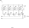
- FIG. 1 illustrates a serial encoder module 100 for serial encoding of non-binary linear block codes.
- the serial encoder module 100 may be configured to generate any P number of parity digits for a K-digit message. However, for purposes of example, the serial encoder module 100 of FIG. 1 is configured to generate 4 parity digits for a K-digit message.
- the serial encoder module 100 includes an input D in , an output D out , 4 single-digit parity shift registers103/103', and a feedback circuit 105 comprising 4 parity generation modules 107. While the serial encoder module 100 of FIG. 1 includes only 4 parity generation modules 107 (e.g. galois field multipliers) and 4 parity shift registers 103/103', a serial encoder module may include any P number of parity shift registers and any P number of parity generation modules corresponding to the P number of parity digits to be generated.
- 4 parity generation modules 107 e.g. galois field multipliers
- the input D in of the encoder module 100 is configured to receive the K-digit message as serial inputs and the output D out of the serial encoder module 100 is configured to output an N-digit coded message with P parity digits.
- the parity generation modules 107 of the feedback circuit 105 are configured to generate parity digits which are stored in the parity shift registers 103/103', as will be discussed in detail below.
- the 4 parity shift registers 103/103' are sequentially coupled, such that an output of a parity shift register 103/103' is coupled to an input of a subsequent parity shift register 103/103' (where a subsequent parity shift register exists).
- Each parity shift register 103/103' corresponds to a parity generation module 107, and each parity generation module 107 is coupled to an input of its corresponding parity shift register 103/103'.
- An adder module A may be associated with an input of each parity shift register 103/103' that is coupled to multiple sources (e.g., parity generation module and preceding parity shift register). The adder modules A facilitate combination of data received at an input of a parity shift register 103/103' for storage.
- An output of a last parity shift register 103' of the 4 parity shift registers 103/103' is coupled to the input D in of the encoder module 100 and also coupled to each parity generation module 107 of the feedback circuit 105.
- the output of the last parity shift register 103' is additionally coupled to the output D out of the encoder module 100 through a multiplexer.
- An additional adder module A may be associated with the output of the last parity shift register 103'.
- the additional adder module A facilitates combination of data received at the output of the last parity shift register 103' for transmission to the parity generation modules 107 of the feedback circuit 105.
- the input D in of the encoder module 100 is similarly coupled to the output D out of the encoder module 100 through the multiplexer.
- the feedback circuit 105 further comprises a switch S.
- the switch S When the switch S is closed, the feedback circuit 105 is active, and the parity generation modules 107 are actively generating parity digits.
- the switch S When the switch S is open, the feedback circuit 105 is deactivated and the parity generation modules 107 no longer generate parity digits.
- the switch S of the feedback circuit 105 is closed.
- a digit of the K-digit message is received at the input D in of the encoder module100 as a serial input, forwarded to the output of the last parity shift register 103', and subsequently forwarded to each parity generation module 107 of the feedback circuit 105.
- Each parity generation module 107 of the feedback circuit 105 is configured to generate a single parity digit, which is stored in a corresponding parity shift register 103, 103'.
- Each parity generation module 107 is configured to generate parity digits for each digit of the K-digit message in accordance with the recursive equation (5) and pseudo code described above. During each clock cycle, the parity digits generated by each parity generation module 107 are combined with the data currently being stored in each corresponding parity shift register 103/103' to form an updated set of parity digits.
- each parity shift register 103, 103' transmits it stored data to a subsequent parity shift register (where there is a subsequent parity shift register).
- the last parity shift register 103' transmits its stored data to each parity generation module 107 of the feedback circuit 105.
- the parity digits stored in the parity shift registers 103/103' are updated each clock cycle, as a new digit of the K-digit message is received and new parity digits are generated by the parity generation modules 107 for storage in the parity shift registers 103/103'.
- the newly generated parity digit are combined with the data currently being stored in corresponding parity shift registers 103/103' to form an updated set of parity digits.
- each digit of the K-digit message received at the input D in of the encoder module 100 is forwarded to the output D out of the encoder module 100 through the multiplexer such that the first K digits output by the encoder module 100 is the K-digit message.
- the switch S of the feedback circuit 105 is open and the final parity digit values stored in the parity shift registers 103/103' are transmitted to the output D out of the encoder module 100.
- the final parity digit values stored in the parity shift registers 103/103' are output in response to control signals CE coupled to each parity shift register 103/103'.
- the parity digits stored in the last parity shift register 103' may be transmitted to the output D out of the encoder module 100 through the multiplexer, and the parity digits stored in each remaining parity shift register 103 may be transmitted to a subsequent parity shift register 103 through a respective adder module.
- the encoder module 100 outputs an N-digit coded message, with the first K digits being the K message digits and the last P digits being the parity digits.
- the encoder module of FIG. 1 operates to encode a K-digit message into an N-digit coded message with P parity digits, it suffers from several disadvantages. Because the encoder module operates in a serial manner, in order to achieve a high line rate, the encoder module must operate at a very high frequency. However, because of the complexity of the logic involved in configuring the parity generation modules, such a high frequency cannot be achieved without introducing various errors into the encoding process and additional costs.
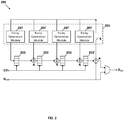
- FIG. 2 One approach for an encoder module that implements parallel encoding of non-binary linear block codes is illustrated in FIG. 2 .
- the serial encoder module 100 of FIG. 1 only a single digit of the K-digit message is processed each clock cycle.
- the encoder module 200 of FIG. 2 allows for multiple digits (L) to be processed each clock cycle.
- the encoder module 200 may be configured to generate any P number of parity digits for a K-digit message to form an N-digit coded message, where the K-digit message is received as L-digit parallel inputs and the N-digit coded message is output as L-digit parallel outputs.
- K is not an integer multiple of L, zeros are inserted at the beginning of the message to achieve an overall message length that is a multiple of L.
- the encoder module 200 includes an input D in , an output D out , 4 4-digit parity shift registers 203/203', and a feedback circuit 205 comprising 4 parity generation modules 207. While the encoder module 200 of FIG. 2 includes only 4 parity generation modules 207 and 4 4-digdigit parity shift registers 203/203', an encoder module 200 may include any P/L number of L-digit parity shift registers and any P/L number of parity generation modules corresponding to the P number of parity digits to be generated and the L-digit parallel inputs being received.
- the input D in of the encoder module 200 is configured to receive the K-digit message as 4-digitdigit parallel inputs and the output D out of the encoding module 200 is configured to output an N-digit coded message with 16 parity digits as 4-digit parallel outputs.
- the parity generation modules 207 of the feedback circuit 205 are each configured to generate 4 parity digits which are stored in the 4-digitdigit parity shift registers 203/203', as will be discussed in detail below.
- the 4 4-digit parity shift registers 203/203' are sequentially coupled, such that an output of a parity shift register 203/203' is coupled to an input of a subsequent parity shift register 203/203' (where a subsequent parity shift register exists).
- Each 4-digitdigit digital parity shift register 203/203' corresponds to a parity generation module 207, and each parity generation module 207 is coupled to an input of its corresponding parity shift register 203/203'.
- An adder module A may be associated with an input of each parity shift register 203/203' that is coupled to multiple sources (e.g., parity generation module and preceding parity shift register). The adder modules A facilitate combination of data received at an input of a parity shift register 203/203' for storage.
- An output of a last parity shift register 203' of the 4 4-digit parity shift registers 203/203' is coupled to the input of the encoder module D in and also coupled to each parity generation module 207of the feedback circuit 209.
- the output of the last parity shift register 203' is additionally coupled to the output D out of the encoder module 200 through a multiplexer.
- An additional adder module A may be associated with the output of the last parity shift register203'.
- the additional adder module A facilitates combination of data received at the output of the last parity shift register 203' for transmission to the parity generation modules 207 of the feedback circuit 205.
- the input D in of the encoder module 200 is also coupled to the output D out of the encoder module 200 through the multiplexer.
- the feedback circuit 205 further comprises a switch S.
- the switch S When the switch S is closed, the feedback circuit 205 is active, and the parity generation modules 207 are actively generating parity digits.
- the switch S When the switch S is open, the feedback circuit 205 is deactivated and the parity generation modules 207 no longer generate parity digits.
- the serial encoder module 100 of FIG. 1 included parity shift registers 103/103' that each stored a single digit
- the encoder module 200 of FIG. 2 includes 4-digitdigit parity shift registers 203/203' that store 4 digits at a time.
- the parity generation modules 207 of the feedback circuit 205 of FIG. 1 processed a single message digit at a time
- the parity generation modules of the feedback circuit of FIG. 2 process 4 message digits at a time.
- the recursive formula (5) for generating parity digits may be extended to support the processing of L digits simultaneously.
- each parity generation module of the feedback circuit generating L parity digits at a time using a P x L parity matrix (PMAT) defined by the following pseudo code. Every L rows of the PMAT forms one parity generation module.
- PMAT P x L parity matrix
- each 4-digit portion of the K-digit message is received at the input D in of the encoder module 200 as a parallel input, forwarded to the output of the last parity shift register 203', and subsequently forwarded to each parity generation module 207 of the feedback circuit 205.
- Each parity generation module 207 of the feedback circuit 205 is configured to generate 4 parity digits (e.g., L parity digits), which are stored in a corresponding 4-digit parity shift register 203/203'.
- Each parity generation module 207 is configured to generate parity digits for each L-digit portion of the K-digit message in accordance with the recursive equation (7), the PMAT matrix, and the pseudo code described above. During each clock cycle, the parity digits generated by each parity generation module 207 are combined with the data currently being stored in each corresponding parity shift register 203/203' to form an updated set of parity digits.
- each parity shift register 203, 203' transmits its stored data to a subsequent parity shift register 203/203' (where there is a subsequent parity shift register).
- the last parity shift register 203' transmits its stored data to each parity generation module 207 of the feedback circuit 205.
- the parity digits stored in the parity shift registers 203/203' are updated each clock cycle, as a new L-digit portion of the K-digit message is received and new parity digits are generated by the parity generation modules 207 for storage in the corresponding parity shift registers 203/203'.
- the newly generated parity digits are combined with the data currently being stored in corresponding parity shift registers 203/203' to form an updated set of parity digits.
- each 4-digit portion of the K-digit message received at the input D in of the encoder module 200 is forwarded to the output D out of the encoder module 200 through the multiplexer such that the first K digits output by the encoder module 200 are 4-digit parallel outputs of the K-digit message.
- the switch S of the feedback circuit 205 is open and the final parity digit values stored in the parity shift registers 203/203' are transmitted to the output D out of the encoder module 200.
- the final parity digit values stored in the parity shift registers 203/203' are output in response to control signals CE coupled to each parity shift register 203/203'.
- the 4 parity digits stored in the last parity shift register 203' may be transmitted to the output D out of the encoder module 200 through the multiplexer, and the 4 parity digits stored in each remaining parity shift register 203 may be transmitted to a subsequent parity shift register 203 through a respective adder module.
- the encoder module 200 outputs an N-digit coded message as 4-digit parallel outputs, with the first K digits being the K message digits and the last P digits being the parity digits.
- parity digits using the PMAT matrix can be efficiently computed as a sum of XORs.
- a parity generation module e.g., serial encoding
- a generator polynomial g(x) defined on a GF(q ⁇ m) Galois Field is used to generate parity digits
- matrix multiplication may require up to m-1 XORs.
- L message digits are being simultaneously processed by a parity generation module and a generator polynomial g(x) defined on a GF(q ⁇ m) Galois Field is used to generate parity digits
- such matrix multiplication may require mL-1 XORs.
- each parity generation module 207 of the feedback circuit 205 is not only performing matrix multiplication on a 4-digit portion of the K-digit message being received, but is additionally performing matrix multiplication on the output of the last parity shift register 203', as each parity generation module 207 is coupled to the input D in of the encoder module 200 and the output of the last parity shift register 203' through the adder module coupled to the output of the last parity shift register 203'.
- 2mL-1 XORs are required to implement each parity generation module 207.
- each parity generation module may form a critical path that limits the speed at which a K-digit message may be encoded into an N-digit coded message.
- the additional computational logic required to implement each parity generation module 207 in FIG. 2 may also result in an increase in hardware resource requirements.
- the encoder module 200 of FIG. 2 may be modified to reduce computational logic required to implement parity generation modules.
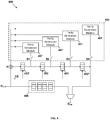
- FIG. 3 illustrates an encoder module 300 that implements parallel encoding of non-binary linear block codes.
- the encoder module 300 of FIG. 3 reduces computational logic required to implement each parity generation module, such that only mL-1 XORs are required to implement a parity generation module as opposed to the 2mL-1 XORs required in the encoder module 200 of FIG. 2 .
- the encoder module 300 of FIG. 3 allows for multiple digits (L) of a K-digit message to be processed each clock cycle, much like the encoder module of FIG. 2 .
- the encoder module 300 may be configured to generate any P number of parity digits for a K-digit message to form an N-digit coded message, where the K-digit message is received as L-digit parallel inputs and the N-digit coded message is output as L-digit parallel outputs.
- K is not an integer multiple of L, zeros are inserted at the beginning of the message to achieve an overall message length that is a multiple of L.
- the encoder module 300 includes an input D in , an output D out , a 4-digit input shift register 301, 4 4-digit parity shift registers 303/303', and a feedback circuit 305 comprising 4 parity generation modules 307. While the encoder module 300 of FIG. 3 includes only 4 parity generation modules 307 and 4 4-digit parity shift registers 303/303', the encoder module 300 may include any P/L number of L-digit parity shift registers and any P/L number of parity generation modules corresponding to the P number of parity digits to be generated and the L-digit parallel inputs being received.
- the input D in of the encoder module 300 is configured to receive the K-digit message as 4-digit parallel inputs and the output D out of the encoder module 300 is configured to output an N-digit coded message with 16 parity digits as 4-digit parallel outputs.
- the parity generation modules 307 of the feedback circuit 305 are each configured to generate 4 parity digits at a time, which are stored in a corresponding 4-digit parity shift register 303/303', as will be discussed in detail below.
- An input of the input shift register 301 is coupled to the input D in of the encoder module 300, and an output of the input shift register 301 is coupled to the output D out of the encoder module 300 through a multiplexer.
- the 4 4-digit parity shift registers 303/303' are sequentially coupled, such that an output of a parity shift register 303/303' is coupled to an input of a subsequent parity shift register 303/303' (where a subsequent parity shift register exists).
- Each 4-digit parity shift register 303/303' corresponds to a parity generation module 307, and each parity generation module 307 is coupled to an input of its corresponding parity shift register 303/303'.
- An input of the last parity shift register 303' of the 4 4-digit parity shift registers 303/303' is coupled to the input D in of the encoder module 300 and an output of the last parity shift register 303' is coupled to each parity generation module 307 of the feedback circuit 305.
- An adder module A may be associated with an input of each parity shift register 303/303' that is coupled to multiple sources (e.g., parity generation module 307, preceding parity shift register 303, input D in of encoder module 300).
- the adder modules A facilitate combination of data received at an input of a parity shift register 303/303' for storage.
- An additional adder module A may be associated with the output of the last parity shift register 303'.
- the additional adder module A facilitates combination of data received at the output of the last parity shift register 303' for transmission to the parity generation modules 307 of the feedback circuit 305.
- the output of the last parity shift register 303' is additionally coupled to the output D out of the encoder module 300 through a multiplexer.
- the feedback circuit 305 further comprises a switch S.
- the switch S When the switch S is closed, the feedback circuit 305 is active, and the parity generation modules 307 are actively generating parity digits.
- the switch S When the switch S is open, the feedback circuit 305 is deactivated and the parity generation modules 307 no longer generate parity digits.
- each 4-digit portion of the K-digit message is received at the input D in of the encoder module 300 as a parallel input and is forwarded to both the input of the last parity shift register 303' and the input of the input shift register 301 during a first clock cycle.
- the 4-digit portion of the K-digit message from the last parity shift register 303' is output into each parity generation module 307 of the feedback circuit 305, each parity generation module 307 thereby generating 4 parity digits that are transmitted to and stored in its corresponding parity shift register 303/303'.
- Each parity generation module 307 is configured to generate parity digits for each digit of the K-digit message in accordance with the following pseudo code.
- the equation for the above pseudo code may be generated by rearranging equation (4) from above as shown below to generate equation (8).
- the 4-digit portion of the K-digit message is output from the input shift register 301 to the output D out of the encoder module 300 through the multiplexer. This continues until all 4-digit portions of the K-digit message have been received.
- each parity shift register 303/303' transmits its stored data to a subsequent parity shift register 303/303' (where there is a subsequent parity shift register).
- the last parity shift register 303' transmits its stored data to each parity generation module 307 of the feedback circuit.
- the parity digits stored in the parity shift registers 303/303' are updated each clock cycle, as a new L-digit portion of the K-digit message is received and new parity digits are generated by the parity generation module 307 for storage in the corresponding parity shift registers 303/303'.
- the newly generated parity digits are combined with the data currently being stored in corresponding parity shift registers 303/303' to form an updated set of parity digits.
- a zero input is received by the input D in of the encoder module 300.
- the zero input causes the encoder module 300 to open the switch S of the feedback circuit 305.
- the last 4-digit portion of the K-digit message in the input shift register 301 is output to the output of the encoder module D out and the last 4-digit portion of the K-digit message in the last parity shift register 303' is output into each parity generation module 307 of the feedback circuit 305 to generate corresponding parity digits prior to the switch S of the feedback circuit 305 opening.
- the switch S of the feedback circuit 305 remains open and the final parity digit values stored in the parity shift registers 303/303' are output to the output D out of the encoder module 300.
- the parity digits are output in response to control signals CE coupled to each of the parity shift registers 303/303'.
- the 4 parity digits stored in the last parity shift register 303' may be transmitted to the output D out of the encoder module 300 through the multiplexer, and the 4 parity digits stored in each remaining parity shift register 303 may be transmitted to a subsequent parity shift register 303/303'.
- each parity generation module 307 By coupling the input of the last parity shift register 303' to the input D in of the encoder module 300 rather than coupling the output of the last parity shift register 303' to the input D in of the encoder module 300, the matrix multiplication being performed by each parity generation module 307 is reduced in complexity. Rather than having to perform matrix multiplication on both the 4-digit portion of the K-digit message being received and the output of the last parity shift register 303' at a given clock cycle, matrix multiplication is only performed on the output of the last parity shift register 303' for a given clock cycle. Thus, rather than requiring 2mL-1 XORs to implement each parity generation module 307, only mL-1 XORs are required to implement each parity generation module 307. This increases the speed at which a K-digit message may be encoded into an N-digit coded message and may also result in a decrease in hardware resource requirements.
- the encoder module 300 of FIG. 3 may be further modified to improve fan-out.
- Fan-out refers to the number of gate inputs a logic gate output is connected to. Fan-out is reduced where the number of gate inputs to which a logic gate output is connected is reduced.
- FIG. 4 illustrates an encoder module 400 for implementing parallel encoding of non-linear block codes with reduced fan-out in accordance with some embodiments.
- the encoder module 400 of FIG. 4 allows for multiple digits (L) of a K-digit message to be processed each clock cycle, much like the encoder module of FIG. 3 .
- the encoder module 400 may be configured to generate any P number of parity digits for a K-digit message to form an N-digit coded message, where the K-digit message is received as L-digit parallel inputs and the N-digit coded message is output as L-digit parallel outputs.
- K is not an integer multiple of L, zeros are inserted at the beginning of the message to achieve an overall message length that is a multiple of L.
- the encoder module 400 includes an input D in , an output D out , a 4 stage delay 409, 4 4-digit parity shift registers 403/403'/403", and a feedback circuit 405 comprising 4 parity generation modules 407. While the encoder module 400 of FIG. 4 includes only 4 parity generation modules 407 and 4 4-digit parity shift registers 403/403'/403", the encoder module 400 may include any P/L number of L-digit parity shift registers and any P/L number of parity generation modules corresponding to the P number of parity digits to be generated and the L-digit parallel inputs being received. Similarly, while the encoder module 400 of FIG. 4 includes only a 4 stage delay 409, the encoder module 400 may include any (P/L) stage delay corresponding to the P number of parity digits to be generated and the L-digit parallel inputs being received.
- the input D in of the encoder module 400 is configured to receive the K-digit message as 4-digit parallel inputs and the output D out of the encoder module 400 is configured to output an N-digit coded message with 16 parity digits as 4-digit parallel outputs.
- the parity generation modules 407 of the feedback circuit 405 are configured to generate parity digits which are stored in the 4-digit parity shift registers, as will be discussed in detail below.
- the 4 4-digit parity shift registers 403/403'/403" are sequentially coupled, such that an output of a parity shift register 403/403'/403" is coupled to an input of a subsequent parity shift register 403/403'/403" (were a subsequent parity shift register exists).
- Each 4-digit parity shift register 403/403'/403" corresponds to a parity generation module 407, and each parity generation module 407 is coupled to an output of its corresponding parity shift register 403/403'/403".
- An input of a first parity shift register 403' is coupled to the input D in of the encoder module 400 as well as the output of each parity generation module 407 of the feedback circuit.
- An adder module A may be associated with the input of the first parity shift register that is coupled to multiple sources (e.g., output of each parity generation module 407 and input D in of encoder module 400).
- the adder module A facilitates combination of data received at the input of the first parity shift register 403' for storage.
- An output of a last parity shift register 403"of the 4 4-digit parity shift registers 403/403'/403" is additionally coupled to the output D out of the encoder module 400 through a multiplexer.
- the 4-stage delay 409 is coupled to the input D in of the of the encoder module 400 and also coupled to the output D out of the encoder module 400 through the multiplexer.
- the feedback circuit 405 further comprises 4 switches S1, S2, S3, S4, wherein each switch S1, S2, S3, S4 corresponds to a parity generation module 407.
- each switch S1, S2, S3, S4 corresponds to a parity generation module 407.
- a switch S1, S2, S3, S4 is closed, its corresponding parity generation module 407 of the feedback circuit 405 is active and generating parity digits.
- a switch S1, S2, S3, S4 is open, its corresponding parity generation module 407 of the feedback circuit 405 is deactivated and no longer generates parity digits.
- each switch S1, S2, S3, S4 of the feedback circuit 405 is closed.
- a 4-digit portion of the K-digit message is received at the input D in of the encoder module 400 and forwarded to the first parity shift register 403'.
- each parity shift register 403/403'/404" transmits it stored data to a corresponding parity generation module 407 and also a subsequent parity shift register 403/403'/403" (where there is a subsequent parity shift register).
- Each parity generation module 407 generates parity digits, which are output back to the first parity shift register 403'.
- the data in the parity shift registers 403/403'/403" form the parity digits.
- the pseudo code may be derived in a manner similar to the derivation of (8) above. At any given cycle, only L parity digits are to be generated rather than the full P parity digits. The total P parity digits will then be generated over P/L clock cycles.
- the 4-digit portion of the K-digit message received at the input D in of the encoder module 400 is passed through the 4-stage delay 409 before being transmitted to the output D out of the encoder module 400 through a multiplexer such that the first K digits output by the encoder module 400 are 4-digit parallel outputs of the K-digit message.
- each parity shift register 403/403' transmits its stored data to a corresponding parity generation module 407 (where the corresponding switch is closed).
- the corresponding parity generation modules 407 generate parity digits which are forwarded to the first input shift register 403'. This is continued until all the switches S1, S2, S3, S4 of the feedback circuit 405 are open.
- the 4 parity digits stored in the last parity shift register403" may be transmitted to the output D out of the encoder module 400 through the multiplexer, and the 4 parity digits stored in each remaining parity shift register 403/403' may be transmitted to a subsequent parity shift register 403/403".
Landscapes
- Physics & Mathematics (AREA)
- Probability & Statistics with Applications (AREA)
- Engineering & Computer Science (AREA)
- Theoretical Computer Science (AREA)
- Mathematical Physics (AREA)
- Algebra (AREA)
- General Physics & Mathematics (AREA)
- Pure & Applied Mathematics (AREA)
- Nonlinear Science (AREA)
- Error Detection And Correction (AREA)
- Detection And Correction Of Errors (AREA)
Applications Claiming Priority (2)
| Application Number | Priority Date | Filing Date | Title |
|---|---|---|---|
| US13/430,222 US8949703B2 (en) | 2012-03-26 | 2012-03-26 | Parallel encoding for non-binary linear block code |
| PCT/US2012/066554 WO2013147935A1 (en) | 2012-03-26 | 2012-11-26 | Parallel encoding for non-binary linear block code |
Publications (2)
| Publication Number | Publication Date |
|---|---|
| EP2831999A1 EP2831999A1 (en) | 2015-02-04 |
| EP2831999B1 true EP2831999B1 (en) | 2019-01-09 |
Family
ID=47470125
Family Applications (1)
| Application Number | Title | Priority Date | Filing Date |
|---|---|---|---|
| EP12808950.5A Active EP2831999B1 (en) | 2012-03-26 | 2012-11-26 | Parallel encoding for non-binary linear block code |
Country Status (6)
| Country | Link |
|---|---|
| US (1) | US8949703B2 (enExample) |
| EP (1) | EP2831999B1 (enExample) |
| JP (1) | JP5978382B2 (enExample) |
| KR (1) | KR101930583B1 (enExample) |
| CN (1) | CN104247274B (enExample) |
| WO (1) | WO2013147935A1 (enExample) |
Families Citing this family (9)
| Publication number | Priority date | Publication date | Assignee | Title |
|---|---|---|---|---|
| CN102820892B (zh) * | 2012-06-20 | 2016-06-01 | 记忆科技(深圳)有限公司 | 一种用于并行bch编码的电路、编码器及方法 |
| US20150363263A1 (en) * | 2014-06-12 | 2015-12-17 | HGST Netherlands B.V. | ECC Encoder Using Partial-Parity Feedback |
| US11611359B2 (en) | 2015-05-29 | 2023-03-21 | SK Hynix Inc. | Data storage device |
| KR20180059150A (ko) * | 2016-11-25 | 2018-06-04 | 에스케이하이닉스 주식회사 | 1 클럭 인코딩이 가능한 에러 정정 코드 인코더 및 에러 정정 코드 인코딩 방법과, 그리고 그 에러 정정 코드 인코더를 포함하는 메모리 컨트롤러 |
| US11515897B2 (en) | 2015-05-29 | 2022-11-29 | SK Hynix Inc. | Data storage device |
| KR102285940B1 (ko) | 2015-05-29 | 2021-08-05 | 에스케이하이닉스 주식회사 | 데이터 처리 회로, 데이터 처리 회로를 포함하는 데이터 저장 장치 및 그것의 동작 방법 |
| US10396827B2 (en) | 2015-09-25 | 2019-08-27 | SK Hynix Inc. | Data storage device |
| US11177835B2 (en) | 2015-09-25 | 2021-11-16 | SK Hynix Inc. | Data storage device |
| KR102683471B1 (ko) * | 2021-05-07 | 2024-07-11 | 한국전자통신연구원 | 병렬 리드솔로몬 부호화 장치 및 방법 |
Family Cites Families (22)
| Publication number | Priority date | Publication date | Assignee | Title |
|---|---|---|---|---|
| US4293951A (en) * | 1979-03-16 | 1981-10-06 | Communications Satellite Corporation | Method and apparatus for encoding/decoding a convolutional code to a periodic convolutional code block |
| US4410989A (en) * | 1980-12-11 | 1983-10-18 | Cyclotomics, Inc. | Bit serial encoder |
| US4777635A (en) * | 1986-08-08 | 1988-10-11 | Data Systems Technology Corp. | Reed-Solomon code encoder and syndrome generator circuit |
| DE69315018T2 (de) * | 1992-08-21 | 1998-04-30 | Koninkl Philips Electronics Nv | Hardware-effizientes Verfahren und Anordnung zur Kodierung von BCH-Kodes und insbesondere Reed-Solomon-Kodes |
| US5383204A (en) * | 1993-06-29 | 1995-01-17 | Mitsubishi Semiconductor America, Inc. | Parallel encoding apparatus and method implementing cyclic redundancy check and Reed-Solomon codes |
| EP1018220B1 (en) * | 1998-08-06 | 2007-07-25 | Samsung Electronics Co., Ltd. | Channel encoding/decoding in communication system |
| US6493845B1 (en) | 1999-06-21 | 2002-12-10 | Maxtor Corporation | Parallel input output combined system for producing error correction code redundancy symbols and error syndromes |
| JP4295871B2 (ja) * | 1999-09-24 | 2009-07-15 | 株式会社東芝 | 誤り訂正復号器 |
| WO2001076077A2 (en) * | 2000-03-31 | 2001-10-11 | Ted Szymanski | Transmitter, receiver, and coding scheme to increase data rate and decrease bit error rate of an optical data link |
| US6895545B2 (en) * | 2002-01-28 | 2005-05-17 | Broadcom Corporation | System and method for generating cyclic codes for error control in digital communications |
| JP2004208282A (ja) * | 2002-12-09 | 2004-07-22 | Sony Corp | データ処理装置 |
| KR101238108B1 (ko) * | 2004-01-15 | 2013-02-27 | 퀄컴 인코포레이티드 | 리드-솔로몬 인코딩 및 디코딩을 수행하는 방법 및 장치 |
| US7565594B2 (en) * | 2004-08-26 | 2009-07-21 | Alcatel-Lucent Usa Inc. | Method and apparatus for detecting a packet error in a wireless communications system with minimum overhead using embedded error detection capability of turbo code |
| US7395492B2 (en) * | 2004-09-13 | 2008-07-01 | Lucent Technologies Inc. | Method and apparatus for detecting a packet error in a wireless communications system with minimum overhead using tail bits in turbo code |
| US7600176B2 (en) * | 2006-03-07 | 2009-10-06 | Broadcom Corporation | Performing multiple Reed-Solomon (RS) software error correction coding (ECC) Galois field computations simultaneously |
| US7831895B2 (en) * | 2006-07-25 | 2010-11-09 | Communications Coding Corporation | Universal error control coding system for digital communication and data storage systems |
| KR20080052039A (ko) * | 2006-12-07 | 2008-06-11 | 삼성전자주식회사 | 순환 중복 검사에 의한 정정 에러를 검사하는 방법 및 그장치 |
| US8286059B1 (en) * | 2007-01-08 | 2012-10-09 | Marvell International Ltd. | Word-serial cyclic code encoder |
| US8151172B2 (en) * | 2008-07-10 | 2012-04-03 | Lsi Corporation | Adjustable error-correction for a reed solomon encoder/decoder |
| CN101834615B (zh) * | 2009-03-12 | 2012-12-26 | 高通创锐讯通讯科技(上海)有限公司 | 里德-索罗蒙编码器实现方法 |
| JP5500357B2 (ja) * | 2010-03-31 | 2014-05-21 | ソニー株式会社 | 符号化装置、および符号化方法 |
| CN102231631B (zh) * | 2011-06-20 | 2018-08-07 | 深圳市中兴微电子技术有限公司 | Rs编码器的编码方法及rs编码器 |
-
2012
- 2012-03-26 US US13/430,222 patent/US8949703B2/en active Active
- 2012-11-26 CN CN201280071938.1A patent/CN104247274B/zh active Active
- 2012-11-26 WO PCT/US2012/066554 patent/WO2013147935A1/en not_active Ceased
- 2012-11-26 JP JP2015503189A patent/JP5978382B2/ja active Active
- 2012-11-26 EP EP12808950.5A patent/EP2831999B1/en active Active
- 2012-11-26 KR KR1020147029911A patent/KR101930583B1/ko active Active
Non-Patent Citations (1)
| Title |
|---|
| None * |
Also Published As
| Publication number | Publication date |
|---|---|
| CN104247274B (zh) | 2019-04-16 |
| US8949703B2 (en) | 2015-02-03 |
| KR20140142320A (ko) | 2014-12-11 |
| US20130254639A1 (en) | 2013-09-26 |
| WO2013147935A1 (en) | 2013-10-03 |
| CN104247274A (zh) | 2014-12-24 |
| JP2015512585A (ja) | 2015-04-27 |
| KR101930583B1 (ko) | 2018-12-18 |
| JP5978382B2 (ja) | 2016-08-24 |
| EP2831999A1 (en) | 2015-02-04 |
Similar Documents
| Publication | Publication Date | Title |
|---|---|---|
| EP2831999B1 (en) | Parallel encoding for non-binary linear block code | |
| Lee | High-speed VLSI architecture for parallel Reed-Solomon decoder | |
| US8108760B2 (en) | Decoding of linear codes with parity check matrix | |
| US6990624B2 (en) | High speed syndrome-based FEC encoder and decoder and system using same | |
| US5440570A (en) | Real-time binary BCH decoder | |
| US11804855B2 (en) | Pipelined forward error correction for vector signaling code channel | |
| CN101795175B (zh) | 数据的校验处理方法及装置 | |
| US9065482B1 (en) | Circuit for forward error correction encoding of data blocks | |
| US6928601B2 (en) | Decoding circuit, and decoder, decoding method and semiconductor device that use the decoding circuit | |
| US20030063554A1 (en) | Combinational circuit, and encoder, decoder and semiconductor device using this combinational circuit | |
| US7458007B2 (en) | Error correction structures and methods | |
| Lee | A VLSI design of a high-speed Reed-Solomon decoder | |
| Wai et al. | Field programmable gate array implementation of Reed-Solomon code, RS (255,239) | |
| Barbosa et al. | FPGA implementation of a Reed-Solomon CODEC for OTN G. 709 standard with reduced decoder area | |
| Salvador et al. | 100Gbit/s FEC for OTN protocol: Design architecture and implementation results | |
| Flocke et al. | Implementation and modeling of parametrizable high-speed Reed Solomon decoders on FPGAs | |
| US20030014713A1 (en) | Signal processing method, signal processing system, program for signal processing, and computer-readable storage medium on which this program is recorded | |
| Rocha | Versatile error-control coding systems | |
| du Preez et al. | A flexible Reed-Solomon codec | |
| Zhang et al. | High speed concatenated code codec for optical communication systems | |
| Lee et al. | A low-complexity, high-speed Reed-Solomon decoder [fiber-optic communication system applications] | |
| Wai | FPGA implementation of Reed Solomon codec for 40Gbps Forward Error Correction in optical networks | |
| Fu et al. | Error Control Coding for On-Chip Interconnects | |
| Qiu et al. | FPGA implementation of Reed-Solomon Codes Based on Visible Light Wireless Communication System | |
| Yuan et al. | Design for High-Speed Optical Networking |
Legal Events
| Date | Code | Title | Description |
|---|---|---|---|
| PUAI | Public reference made under article 153(3) epc to a published international application that has entered the european phase |
Free format text: ORIGINAL CODE: 0009012 |
|
| 17P | Request for examination filed |
Effective date: 20140911 |
|
| AK | Designated contracting states |
Kind code of ref document: A1 Designated state(s): AL AT BE BG CH CY CZ DE DK EE ES FI FR GB GR HR HU IE IS IT LI LT LU LV MC MK MT NL NO PL PT RO RS SE SI SK SM TR |
|
| AX | Request for extension of the european patent |
Extension state: BA ME |
|
| DAX | Request for extension of the european patent (deleted) | ||
| STAA | Information on the status of an ep patent application or granted ep patent |
Free format text: STATUS: EXAMINATION IS IN PROGRESS |
|
| 17Q | First examination report despatched |
Effective date: 20170627 |
|
| GRAP | Despatch of communication of intention to grant a patent |
Free format text: ORIGINAL CODE: EPIDOSNIGR1 |
|
| STAA | Information on the status of an ep patent application or granted ep patent |
Free format text: STATUS: GRANT OF PATENT IS INTENDED |
|
| INTG | Intention to grant announced |
Effective date: 20180821 |
|
| GRAS | Grant fee paid |
Free format text: ORIGINAL CODE: EPIDOSNIGR3 |
|
| GRAA | (expected) grant |
Free format text: ORIGINAL CODE: 0009210 |
|
| STAA | Information on the status of an ep patent application or granted ep patent |
Free format text: STATUS: THE PATENT HAS BEEN GRANTED |
|
| AK | Designated contracting states |
Kind code of ref document: B1 Designated state(s): AL AT BE BG CH CY CZ DE DK EE ES FI FR GB GR HR HU IE IS IT LI LT LU LV MC MK MT NL NO PL PT RO RS SE SI SK SM TR |
|
| REG | Reference to a national code |
Ref country code: GB Ref legal event code: FG4D |
|
| REG | Reference to a national code |
Ref country code: CH Ref legal event code: EP Ref country code: AT Ref legal event code: REF Ref document number: 1088609 Country of ref document: AT Kind code of ref document: T Effective date: 20190115 |
|
| REG | Reference to a national code |
Ref country code: IE Ref legal event code: FG4D |
|
| REG | Reference to a national code |
Ref country code: DE Ref legal event code: R096 Ref document number: 602012055793 Country of ref document: DE |
|
| REG | Reference to a national code |
Ref country code: NL Ref legal event code: MP Effective date: 20190109 |
|
| REG | Reference to a national code |
Ref country code: LT Ref legal event code: MG4D |
|
| PG25 | Lapsed in a contracting state [announced via postgrant information from national office to epo] |
Ref country code: NL Free format text: LAPSE BECAUSE OF FAILURE TO SUBMIT A TRANSLATION OF THE DESCRIPTION OR TO PAY THE FEE WITHIN THE PRESCRIBED TIME-LIMIT Effective date: 20190109 |
|
| REG | Reference to a national code |
Ref country code: AT Ref legal event code: MK05 Ref document number: 1088609 Country of ref document: AT Kind code of ref document: T Effective date: 20190109 |
|
| PG25 | Lapsed in a contracting state [announced via postgrant information from national office to epo] |
Ref country code: PL Free format text: LAPSE BECAUSE OF FAILURE TO SUBMIT A TRANSLATION OF THE DESCRIPTION OR TO PAY THE FEE WITHIN THE PRESCRIBED TIME-LIMIT Effective date: 20190109 Ref country code: LT Free format text: LAPSE BECAUSE OF FAILURE TO SUBMIT A TRANSLATION OF THE DESCRIPTION OR TO PAY THE FEE WITHIN THE PRESCRIBED TIME-LIMIT Effective date: 20190109 Ref country code: FI Free format text: LAPSE BECAUSE OF FAILURE TO SUBMIT A TRANSLATION OF THE DESCRIPTION OR TO PAY THE FEE WITHIN THE PRESCRIBED TIME-LIMIT Effective date: 20190109 Ref country code: PT Free format text: LAPSE BECAUSE OF FAILURE TO SUBMIT A TRANSLATION OF THE DESCRIPTION OR TO PAY THE FEE WITHIN THE PRESCRIBED TIME-LIMIT Effective date: 20190509 Ref country code: ES Free format text: LAPSE BECAUSE OF FAILURE TO SUBMIT A TRANSLATION OF THE DESCRIPTION OR TO PAY THE FEE WITHIN THE PRESCRIBED TIME-LIMIT Effective date: 20190109 Ref country code: SE Free format text: LAPSE BECAUSE OF FAILURE TO SUBMIT A TRANSLATION OF THE DESCRIPTION OR TO PAY THE FEE WITHIN THE PRESCRIBED TIME-LIMIT Effective date: 20190109 Ref country code: NO Free format text: LAPSE BECAUSE OF FAILURE TO SUBMIT A TRANSLATION OF THE DESCRIPTION OR TO PAY THE FEE WITHIN THE PRESCRIBED TIME-LIMIT Effective date: 20190409 |
|
| PG25 | Lapsed in a contracting state [announced via postgrant information from national office to epo] |
Ref country code: GR Free format text: LAPSE BECAUSE OF FAILURE TO SUBMIT A TRANSLATION OF THE DESCRIPTION OR TO PAY THE FEE WITHIN THE PRESCRIBED TIME-LIMIT Effective date: 20190410 Ref country code: IS Free format text: LAPSE BECAUSE OF FAILURE TO SUBMIT A TRANSLATION OF THE DESCRIPTION OR TO PAY THE FEE WITHIN THE PRESCRIBED TIME-LIMIT Effective date: 20190509 Ref country code: LV Free format text: LAPSE BECAUSE OF FAILURE TO SUBMIT A TRANSLATION OF THE DESCRIPTION OR TO PAY THE FEE WITHIN THE PRESCRIBED TIME-LIMIT Effective date: 20190109 Ref country code: HR Free format text: LAPSE BECAUSE OF FAILURE TO SUBMIT A TRANSLATION OF THE DESCRIPTION OR TO PAY THE FEE WITHIN THE PRESCRIBED TIME-LIMIT Effective date: 20190109 Ref country code: BG Free format text: LAPSE BECAUSE OF FAILURE TO SUBMIT A TRANSLATION OF THE DESCRIPTION OR TO PAY THE FEE WITHIN THE PRESCRIBED TIME-LIMIT Effective date: 20190409 Ref country code: RS Free format text: LAPSE BECAUSE OF FAILURE TO SUBMIT A TRANSLATION OF THE DESCRIPTION OR TO PAY THE FEE WITHIN THE PRESCRIBED TIME-LIMIT Effective date: 20190109 |
|
| REG | Reference to a national code |
Ref country code: DE Ref legal event code: R097 Ref document number: 602012055793 Country of ref document: DE |
|
| PG25 | Lapsed in a contracting state [announced via postgrant information from national office to epo] |
Ref country code: AT Free format text: LAPSE BECAUSE OF FAILURE TO SUBMIT A TRANSLATION OF THE DESCRIPTION OR TO PAY THE FEE WITHIN THE PRESCRIBED TIME-LIMIT Effective date: 20190109 Ref country code: CZ Free format text: LAPSE BECAUSE OF FAILURE TO SUBMIT A TRANSLATION OF THE DESCRIPTION OR TO PAY THE FEE WITHIN THE PRESCRIBED TIME-LIMIT Effective date: 20190109 Ref country code: RO Free format text: LAPSE BECAUSE OF FAILURE TO SUBMIT A TRANSLATION OF THE DESCRIPTION OR TO PAY THE FEE WITHIN THE PRESCRIBED TIME-LIMIT Effective date: 20190109 Ref country code: SK Free format text: LAPSE BECAUSE OF FAILURE TO SUBMIT A TRANSLATION OF THE DESCRIPTION OR TO PAY THE FEE WITHIN THE PRESCRIBED TIME-LIMIT Effective date: 20190109 Ref country code: IT Free format text: LAPSE BECAUSE OF FAILURE TO SUBMIT A TRANSLATION OF THE DESCRIPTION OR TO PAY THE FEE WITHIN THE PRESCRIBED TIME-LIMIT Effective date: 20190109 Ref country code: EE Free format text: LAPSE BECAUSE OF FAILURE TO SUBMIT A TRANSLATION OF THE DESCRIPTION OR TO PAY THE FEE WITHIN THE PRESCRIBED TIME-LIMIT Effective date: 20190109 Ref country code: DK Free format text: LAPSE BECAUSE OF FAILURE TO SUBMIT A TRANSLATION OF THE DESCRIPTION OR TO PAY THE FEE WITHIN THE PRESCRIBED TIME-LIMIT Effective date: 20190109 Ref country code: AL Free format text: LAPSE BECAUSE OF FAILURE TO SUBMIT A TRANSLATION OF THE DESCRIPTION OR TO PAY THE FEE WITHIN THE PRESCRIBED TIME-LIMIT Effective date: 20190109 |
|
| PLBE | No opposition filed within time limit |
Free format text: ORIGINAL CODE: 0009261 |
|
| STAA | Information on the status of an ep patent application or granted ep patent |
Free format text: STATUS: NO OPPOSITION FILED WITHIN TIME LIMIT |
|
| PG25 | Lapsed in a contracting state [announced via postgrant information from national office to epo] |
Ref country code: SM Free format text: LAPSE BECAUSE OF FAILURE TO SUBMIT A TRANSLATION OF THE DESCRIPTION OR TO PAY THE FEE WITHIN THE PRESCRIBED TIME-LIMIT Effective date: 20190109 |
|
| 26N | No opposition filed |
Effective date: 20191010 |
|
| PG25 | Lapsed in a contracting state [announced via postgrant information from national office to epo] |
Ref country code: SI Free format text: LAPSE BECAUSE OF FAILURE TO SUBMIT A TRANSLATION OF THE DESCRIPTION OR TO PAY THE FEE WITHIN THE PRESCRIBED TIME-LIMIT Effective date: 20190109 |
|
| PG25 | Lapsed in a contracting state [announced via postgrant information from national office to epo] |
Ref country code: TR Free format text: LAPSE BECAUSE OF FAILURE TO SUBMIT A TRANSLATION OF THE DESCRIPTION OR TO PAY THE FEE WITHIN THE PRESCRIBED TIME-LIMIT Effective date: 20190109 |
|
| REG | Reference to a national code |
Ref country code: CH Ref legal event code: PL |
|
| PG25 | Lapsed in a contracting state [announced via postgrant information from national office to epo] |
Ref country code: CH Free format text: LAPSE BECAUSE OF NON-PAYMENT OF DUE FEES Effective date: 20191130 Ref country code: LU Free format text: LAPSE BECAUSE OF NON-PAYMENT OF DUE FEES Effective date: 20191126 Ref country code: MC Free format text: LAPSE BECAUSE OF FAILURE TO SUBMIT A TRANSLATION OF THE DESCRIPTION OR TO PAY THE FEE WITHIN THE PRESCRIBED TIME-LIMIT Effective date: 20190109 Ref country code: LI Free format text: LAPSE BECAUSE OF NON-PAYMENT OF DUE FEES Effective date: 20191130 |
|
| REG | Reference to a national code |
Ref country code: BE Ref legal event code: MM Effective date: 20191130 |
|
| PG25 | Lapsed in a contracting state [announced via postgrant information from national office to epo] |
Ref country code: BE Free format text: LAPSE BECAUSE OF NON-PAYMENT OF DUE FEES Effective date: 20191130 |
|
| PG25 | Lapsed in a contracting state [announced via postgrant information from national office to epo] |
Ref country code: CY Free format text: LAPSE BECAUSE OF FAILURE TO SUBMIT A TRANSLATION OF THE DESCRIPTION OR TO PAY THE FEE WITHIN THE PRESCRIBED TIME-LIMIT Effective date: 20190109 |
|
| PG25 | Lapsed in a contracting state [announced via postgrant information from national office to epo] |
Ref country code: MT Free format text: LAPSE BECAUSE OF FAILURE TO SUBMIT A TRANSLATION OF THE DESCRIPTION OR TO PAY THE FEE WITHIN THE PRESCRIBED TIME-LIMIT Effective date: 20190109 Ref country code: HU Free format text: LAPSE BECAUSE OF FAILURE TO SUBMIT A TRANSLATION OF THE DESCRIPTION OR TO PAY THE FEE WITHIN THE PRESCRIBED TIME-LIMIT; INVALID AB INITIO Effective date: 20121126 |
|
| PG25 | Lapsed in a contracting state [announced via postgrant information from national office to epo] |
Ref country code: MK Free format text: LAPSE BECAUSE OF FAILURE TO SUBMIT A TRANSLATION OF THE DESCRIPTION OR TO PAY THE FEE WITHIN THE PRESCRIBED TIME-LIMIT Effective date: 20190109 |
|
| P01 | Opt-out of the competence of the unified patent court (upc) registered |
Effective date: 20230530 |
|
| PGFP | Annual fee paid to national office [announced via postgrant information from national office to epo] |
Ref country code: DE Payment date: 20241008 Year of fee payment: 13 |
|
| PGFP | Annual fee paid to national office [announced via postgrant information from national office to epo] |
Ref country code: GB Payment date: 20241105 Year of fee payment: 13 |
|
| PGFP | Annual fee paid to national office [announced via postgrant information from national office to epo] |
Ref country code: FR Payment date: 20241129 Year of fee payment: 13 |
|
| PGFP | Annual fee paid to national office [announced via postgrant information from national office to epo] |
Ref country code: IE Payment date: 20241018 Year of fee payment: 13 |