EP2830402B1 - Frequenzumrichter - Google Patents
Frequenzumrichter Download PDFInfo
- Publication number
- EP2830402B1 EP2830402B1 EP14162713.3A EP14162713A EP2830402B1 EP 2830402 B1 EP2830402 B1 EP 2830402B1 EP 14162713 A EP14162713 A EP 14162713A EP 2830402 B1 EP2830402 B1 EP 2830402B1
- Authority
- EP
- European Patent Office
- Prior art keywords
- circuit board
- printed circuit
- moulded body
- frequency converter
- plastic moulded
- Prior art date
- Legal status (The legal status is an assumption and is not a legal conclusion. Google has not performed a legal analysis and makes no representation as to the accuracy of the status listed.)
- Active
Links
Images


Classifications
-
- H—ELECTRICITY
- H02—GENERATION; CONVERSION OR DISTRIBUTION OF ELECTRIC POWER
- H02M—APPARATUS FOR CONVERSION BETWEEN AC AND AC, BETWEEN AC AND DC, OR BETWEEN DC AND DC, AND FOR USE WITH MAINS OR SIMILAR POWER SUPPLY SYSTEMS; CONVERSION OF DC OR AC INPUT POWER INTO SURGE OUTPUT POWER; CONTROL OR REGULATION THEREOF
- H02M7/00—Conversion of AC power input into DC power output; Conversion of DC power input into AC power output
- H02M7/003—Constructional details, e.g. physical layout, assembly, wiring or busbar connections
-
- H—ELECTRICITY
- H05—ELECTRIC TECHNIQUES NOT OTHERWISE PROVIDED FOR
- H05K—PRINTED CIRCUITS; CASINGS OR CONSTRUCTIONAL DETAILS OF ELECTRIC APPARATUS; MANUFACTURE OF ASSEMBLAGES OF ELECTRICAL COMPONENTS
- H05K7/00—Constructional details common to different types of electric apparatus
- H05K7/14—Mounting supporting structure in casing or on frame or rack
- H05K7/1417—Mounting supporting structure in casing or on frame or rack having securing means for mounting boards, plates or wiring boards
- H05K7/142—Spacers not being card guides
-
- H—ELECTRICITY
- H05—ELECTRIC TECHNIQUES NOT OTHERWISE PROVIDED FOR
- H05K—PRINTED CIRCUITS; CASINGS OR CONSTRUCTIONAL DETAILS OF ELECTRIC APPARATUS; MANUFACTURE OF ASSEMBLAGES OF ELECTRICAL COMPONENTS
- H05K7/00—Constructional details common to different types of electric apparatus
- H05K7/14—Mounting supporting structure in casing or on frame or rack
- H05K7/1422—Printed circuit boards receptacles, e.g. stacked structures, electronic circuit modules or box like frames
- H05K7/1427—Housings
- H05K7/1432—Housings specially adapted for power drive units or power converters
- H05K7/14322—Housings specially adapted for power drive units or power converters wherein the control and power circuits of a power converter are arranged within the same casing
Definitions
- the invention relates to a frequency converter.
- the not pre-released EP 2 639 943 A1 shows an electric motor with an electronics housing, which has a removable cover and an operating unit.
- the DE 199 28 400 A1 shows a touch-proof electrical high-voltage supply, which has a first housing part, which is used for the outer cover. Furthermore, a second housing part forming two sides is provided, on the first side of which a high-voltage supply part and on the second side of which a low-voltage supply part, spatially separated from the high-voltage supply part, are arranged.
- the US 5,930,112 A shows a wireless engine control unit.
- the DE 10 2011 010 431 A1 shows a frequency converter with a circuit board, which is at least partially surrounded by a plastic body and is connected to this material and / or form-fitting. As a result, the circuit board is protected from mechanical influences, such as force shocks, shocks or the like.
- the EP 1 176 706 A2 shows a frequency converter with an upper part and a lower part.
- the invention has for its object to provide a frequency converter which prevents contact with areas with hazardous voltages and which is easy to assemble and disassemble.
- the frequency converter has at least one circuit board with areas to be protected against contact, i.e. Areas that may carry hazardous voltages and / or are sensitive to ESD (electrostatic discharge).
- the frequency converter furthermore has a spatially shaped plastic molded body with holding means which can be operated, in particular without tools.
- the holding means are designed to releasably mechanically fix or hold and / or support the printed circuit board in the molded plastic body, the areas of the printed circuit board to be protected against contact being covered by the molded plastic body at least on one side of the printed circuit board in such a way that the printed circuit board is fixed in the plastic molded body contact by a hand or a finger is prevented.
- the molded plastic body thus serves on the one hand as protection against contact and on the other hand as a mechanical receptacle and fixation of the printed circuit board, which mechanically fixes the printed circuit board in such a way that it does not have to be additionally mechanically fixed to a housing, for example.
- the frequency converter also has a housing in which the molded plastic body and the printed circuit board fixed in the molded plastic body are arranged. Due to the fixing of the circuit board by the holding means in the plastic molding, there is no need to mechanically connect the circuit board to the housing. This reduces the assembly effort. Furthermore, the number of holding means can be chosen to be large enough that a secure mechanical fixing to all relevant areas of the printed circuit board is possible without, for example, having to provide a correspondingly large number of screw connections.
- the holding means can each have a locking mechanism or locking means.
- the circuit board can be inserted or pressed into an opening provided for this purpose in the molded plastic body, the respective latching mechanism of the holding means causing the circuit board to be locked in place from a certain insertion position.
- At least one releasable clamp or plug connector or the like can be arranged on the printed circuit board, the holding means being arranged in such a way that they mechanically fix or support the printed circuit board specifically in the region of the at least one clamp or plug connector in order to prevent unwanted deformations when a force is applied in the To prevent pulling or plugging.
- the holding means can be designed in such a way that the printed circuit board can only be detached from the molded plastic body if the molded plastic body and the printed circuit board fixed in the molded plastic body are not inserted into the housing.
- the molded plastic body can be designed in such a way that the clamping or plug connectors are accessible to a user.
- the molded plastic body can have corresponding openings or cutouts, for example.
- the molded plastic body can have function module holding means that are designed to mechanically fix function modules that are provided mechanically separated from the printed circuit board at a predetermined position.
- the function module holding means can have guide means which are designed to mechanically guide one or more contact pins of the function module in such a way that associated contact areas of the printed circuit board are reliably contacted, for example in the course of a plug-on operation.
- the function module can be a wireless data transmission module, for example an RFID or transponder module.
- the molded plastic body can have preformed areas or depressions 8 for guiding and fixing flexible electrical conductors or cables, and in this way ensure safe cable routing.
- the molded plastic body can be mechanically coupled to the housing by means of a screw connection, for example exactly one.
- At least one power semiconductor component for example an insulated-gate bipolar transistor (IGBT) module, is arranged on the printed circuit board, to which a pressure plate is assigned, the pressure plate being formed in the plastic molded body or being formed by means of the plastic molded body.
- IGBT insulated-gate bipolar transistor
- Fig. 1 shows an exploded perspective view of a frequency converter 100.
- the frequency converter 100 has a housing comprising an upper housing part or a housing cover 4a made of plastic and a lower housing part 4b made of die-cast aluminum.
- the lower housing part 4b has closable openings 11 for cable passage.
- the frequency converter 100 furthermore has a spatially shaped plastic molded body 2, which is inserted into the housing formed from the housing parts 4a and 4b in a completely assembled state of the frequency converter 100.
- the frequency converter 100 also has a printed circuit board 1, on which components are conventionally arranged which serve to control the function of the frequency converter 100.
- the circuit board 1 has, on its side facing the upper housing part 4a, various areas which can carry a voltage which is hazardous to health and are therefore to be protected against contact.
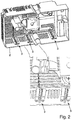
- the molded plastic body 2 has a number of latching means 3 (see Fig. 2 ), which are designed to mechanically detachably fix the circuit board 1 in the molded plastic body 2. It goes without saying that holding means 3 can be provided at corresponding positions on the non-visible side of the plastic molded body 2.
- the circuit board 1 is inserted or pressed into the plastic molded body 2, for example, from below until the circuit board 1 engages in the respective latching or holding means 3 on the corresponding circuit board regions. By expanding the plastic molded body 2, the circuit board 1 can be removed from the plastic molded body 2 again.
- the holding means 3 are designed in such a way that the circuit board 1 can only be detached from the plastic molded body 2 if the plastic molded body 2 and the printed circuit board 1 fixed in the plastic molded body 2 are not inserted into the housing or the lower housing part 4b.
- the molded plastic body 2 and the printed circuit board 1 fixed in the molded plastic body 2 are first inserted into the lower housing part 4b in the course of an assembly process, the molded plastic body 2 being screwed to the lower housing part 4b by means of a single screw connection.
- the molded plastic body 2 has a through hole 11 (see Fig. 2 ), through which a threaded screw can be inserted, which can be screwed into a corresponding threaded hole in the lower housing part 4b.
- the cover or the upper housing part 4a is then screwed to the lower housing part 4b.
- the molded plastic body 2 covers the areas of the printed circuit board 1 that are to be protected from contact, so that these areas cannot be touched. A contact from the bottom is also excluded due to the lower housing part 4b.
- a plurality of clamps or plug connectors 5a, 5b, 5c are arranged on the printed circuit board 1, the holding means 3 being distributed over the molded plastic body 2 such that they mechanically fix the printed circuit board 1, in particular in the area of these clamps or plug connectors 5a, 5b, 5c, ie support the printed circuit board 1 in these areas, so that mechanical deformation upon application of force is prevented.
- the molded plastic body 2 is provided with openings in such a way that the clamping or plug connectors 5a, 5b, 5c are accessible to a user when the upper housing part 4a is removed.
- the plastic molded body 2 has on its upper side functional module holding means 6, which are designed to mechanically detachably fix a functional module in the form of a radio frequency identification (RFID) module 7.
- RFID module can be, for example, an RFID transponder antenna or an RFID transponder with an associated antenna.
- the RFID module 7 is in Fig. 1 schematically represented "floating" in its mounting position for reasons of illustration. It goes without saying that the RFID module 7 is different than in FIG Fig. 1 shown, is fixed in the function module holding means 6.
- the function module holding means 6 have locking means 9 for releasable locking of the RFID module 7 (see Fig. 3 ).
- the functional module holding means 6 also have guide means 12 which are designed to guide contact pins of the functional module 7, not shown in any more detail, in such a way that associated contact areas of the printed circuit board 1 are reliably contacted during assembly.
- a power semiconductor component in the form of an IGBT module is arranged on the printed circuit board 1, to which a pressure plate 10 (in Fig. 1 assigned as a single component for reasons of illustration), the pressure plate 10 being part of the plastic molded body 2.
- a pressure plate 10 in Fig. 1 assigned as a single component for reasons of illustration, the pressure plate 10 being part of the plastic molded body 2.
- pressure plates enable an improved thermal coupling of the IGBT module to an associated heat sink (not shown) and are usually to be fitted as a separate component for a respective power semiconductor component.
- the pressure plate 10 By integrating the pressure plate 10 into the plastic molded body 2, the component costs decrease and the assembly effort is reduced.
Landscapes
- Engineering & Computer Science (AREA)
- Microelectronics & Electronic Packaging (AREA)
- Power Engineering (AREA)
- Casings For Electric Apparatus (AREA)
Description
- Die Erfindung betrifft einen Frequenzumrichter.
- Bei der Inbetriebnahme von Frequenzumrichtern im Feld ist es unter Umständen notwendig, von außen zugeführte elektrische Anschlussleitungen innerhalb des Frequenzumrichters an Klemm- und/oder Steckverbinder des Frequenzumrichters anzuschließen. Im Zuge dieser Arbeiten besteht die Gefahr, dass Bereiche mit gefährdenden Spannungen berührt werden.
- Die nicht vorveröffentlichte
EP 2 639 943 A1 zeigt einen Elektromotor mit einem Elektronikgehäuse, welches einen abnehmbaren Deckel sowie eine Bedieneinheit aufweist. - Die
DE 199 28 400 A1 zeigt eine berührungssichere elektrische Hochspannungsversorgung, die ein erstes Gehäuseteil aufweist, das zur äußeren Abdeckung dient. Weiter ist ein zweites zwei Seiten bildendes Gehäuseteil vorgesehen, auf dessen erster Seite ein Hochspannungsversorgungsteil und auf dessen zweiter Seite ein Niederspannungsversorgungsteil, von dem Hochspannungsversorgungsteil räumlich getrennt, angeordnet sind. - Die
US 5,930,112 A zeigt eine drahtlose Motorsteuereinheit. - Die
DE 10 2011 010 431 A1 zeigt einen Frequenzumrichter mit einer Leiterplatte, die zumindest teilweise von einem Kunststoffkörper umgeben ist und mit diesem stoff- und/oder formschlüssig verbunden ist. Dadurch ist die Leiterplatte vor mechanischen Einwirkungen, wie Kraftstößen, Erschütterungen oder dergleichen geschützt. - Die
EP 1 176 706 A2 zeigt einen Frequenzumrichter mit einem Oberteil und einem Unterteil. - Der Erfindung liegt die Aufgabe zugrunde, einen Frequenzumrichter zur Verfügung zu stellen, der eine Berührung von Bereichen mit gefährdenden Spannungen verhindert und der einfach montierbar und demontierbar ist.
- Die Erfindung löst diese Aufgabe durch einen Frequenzumrichter nach Anspruch 1. Bevorzugte Ausführungsformen sind Gegenstand der Unteransprüche.
- Der Frequenzumrichter weist mindestens eine Leiterplatte mit gegenüber Berührung zu schützenden Bereichen auf, d.h. Bereichen, die möglicherweise gesundheitsgefährdende Spannungen führen und/oder empfindlich gegenüber ESD (elektrostatische Entladung) sind.
- Der Frequenzumrichter weist weiter einen räumlich geformten Kunststoffformkörper mit, insbesondere werkzeuglos, bedienbaren Haltemitteln auf. Die Haltemittel sind dazu ausgebildet, die Leiterplatte im Kunststoffformkörper lösbar mechanisch zu fixieren bzw. zu halten und/oder zu stützen, wobei die gegenüber Berührung zu schützenden Bereiche der Leiterplatte bei im Kunststoffformkörper fixierter Leiterplatte zumindest auf einer Leiterplattenseite derart durch den Kunststoffformkörper überdeckt sind, dass eine Berührung durch eine Hand bzw. einen Finger verhindert wird. Der Kunststoffformkörper dient folglich einerseits als Berührschutz und andererseits als mechanische Aufnahme und Fixierung der Leiterplatte, die die Leiterplatte derart mechanisch fixiert, dass diese beispielsweise nicht zusätzlich mechanisch an einem Gehäuse fixiert werden muss.
- Der Frequenzumrichter weist weiter ein Gehäuse auf, in dem der Kunststoffformkörper sowie die im Kunststoffformkörper fixierte Leiterplatte angeordnet sind. Aufgrund der Fixierung der Leiterplatte durch die Haltemittel im Kunststoffformkörper entfällt die Notwendigkeit, die Leiterplatte mit dem Gehäuse mechanisch zu verbinden. Dies reduziert den Montageaufwand. Weiter kann die Anzahl der Haltemittel derart groß gewählt werden, dass eine sichere mechanische Fixierung an sämtlichen relevanten Bereichen der Leiterplatte möglich ist, ohne dass hierzu beispielsweise eine entsprechend große Anzahl an Verschraubungen vorgesehen werden muss.
- Die Haltemittel können jeweils einen Rastmechanismus bzw. Rastmitel aufweisen. Beispielsweise kann die Leiterplatte in eine hierfür vorgesehene Öffnung des Kunststoffformkörpers eingeschoben bzw. eingedrückt werden, wobei der jeweilige Rastmechanismus der Haltemittel ein verrastendes Fixieren der Leiterplatte ab einer bestimmten Einschubposition bewirkt.
- Auf der Leiterplatte kann mindestens ein lösbarer Klemm- oder Steckverbinder oder dergleichen angeordnet sein, wobei die Haltemittel derart angeordnet sind, dass sie die Leiterplatte spezifisch im Bereich des mindestens einen Klemm- oder Steckverbinders mechanisch fixieren bzw. unterstützen, um ungewollte Verformungen bei einer Kraftbeaufschlagung im Zuge eines Klemm- oder Steckvorgangs zu verhindern.
- Die Haltemittel können derart ausgebildet sein, dass ein Lösen der Leiterplatte aus dem Kunststoffformkörper nur dann möglich ist, wenn der Kunststoffformkörper sowie die im Kunststoffformkörper fixierte Leiterplatte nicht in das Gehäuse eingesetzt sind.
- Der Kunststoffformkörper kann derart ausgebildet sein, dass die Klemm- oder Steckverbinder für einen Benutzer zugänglich sind. Der Kunststoffformkörper kann hierzu beispielsweise entsprechende Öffnungen bzw. Aussparungen aufweisen.
- Der Kunststoffformkörper kann Funktionsmodulhaltemittel aufweisen, die dazu ausgebildet sind, Funktionsmodule, die von der Leiterplatte mechanisch getrennt vorgesehen sind, mechanisch an einer vorgegebenen Position zu fixieren.
- Die Funktionsmodulhaltemittel können Führungsmittel aufweisen, die dazu ausgebildet sind, einen oder mehrere Kontaktstifte des Funktionsmoduls derart mechanisch zu führen, dass zugehörige Kontaktbereiche der Leiterplatte, beispielswiese im Zuge eines Aufsteckvorgangs, sicher kontaktiert werden.
- Das Funktionsmodul kann ein drahtloses Datenübertragungsmodul sein, beispielsweise ein RFID- oder Transponder-Modul.
- Der Kunststoffformkörper kann vorgeformte Bereiche bzw. Vertiefungen 8 zur Führung und Fixierung flexibler elektrischer Leiter bzw. Kabel aufweisen, und auf diese Weise eine sichere Kabelführung gewährleisten.
- Der Kunststoffformkörper kann mittels einer, beispielsweise genau einer, Schraubverbindung mit dem Gehäuse mechanisch gekoppelt werden.
- Auf der Leiterplatte ist mindestens ein Leistungshalbleiterbauelement, beispielsweise ein insulated-gate bipolar Transistor (IGBT)-Modul, angeordnet, dem eine Andruckplatte zugeordnet ist, wobei die Andruckplatte in dem Kunststoffformkörper ausgebildet bzw. mittels des Kunststoffformkörpers gebildet ist. Andruckplatten ermöglichen durch Kraftbeaufschlagung eine verbesserte thermische Ankopplung des Leistungshalbleiterbauelements an einen zugehörigen Kühlkörper und sind in der Regel als eigenes Bauelement für ein jeweiliges Leistungshalbleiterbauelement zu bestücken. Durch Integration der Andruckplatte in den Kunststoffformkörper sinken die Bauelementkosten und der Montageaufwand wird reduziert.
- Die Erfindung wird nachfolgend unter Bezugnahme auf die Zeichnungen detailliert beschrieben. Hierbei zeigt schematisch:
- Fig. 1
- eine perspektivische Explosionsdarstellung eines Frequenzumrichters,
- Fig. 2
- eine perspektivische Darstellung eines Kunststoffformkörpers des in
Fig. 1 gezeigten Frequenzumrichters und - Fig. 3
- Funktionsmodulhaltemittel des in
Fig. 2 gezeigten Kunststoffformkörpers. -
Fig. 1 zeigt eine perspektivische Explosionsdarstellung eines Frequenzumrichters 100. - Der Frequenzumrichter 100 weist ein Gehäuse umfassend ein Gehäuseoberteil bzw. einen Gehäusedeckel 4a aus Kunststoff und ein Gehäuseunterteil 4b aus Aluminiumdruckguss auf. Das Gehäuseunterteil 4b weist verschließbare Öffnungen 11 zur Kabeldurchführung auf.
- Der Frequenzumrichter 100 weist weiter einen räumlich geformten Kunststoffformkörper 2 auf, der in einem fertig montierten Zustand des Frequenzumrichters 100 in das aus den Gehäuseteilen 4a und 4b gebildete Gehäuse eingesetzt ist.
- Der Frequenzumrichter 100 weist weiter eine Leiterplatte 1 auf, auf der herkömmlich Bauelemente angeordnet sind, die zur Funktionssteuerung des Frequenzumrichters 100 dienen. Die Leiterplatte 1 weist auf ihrer dem Gehäuseoberteil 4a zuzuwendenden Seite verschiedene Bereiche auf, die eine gesundheitsgefährdende Spannung führen können und daher gegenüber Berührung zu schützen sind.
- Der Kunststoffformkörper 2 weist eine Anzahl von rastend wirkenden Haltemitteln 3 (siehe
Fig. 2 ) auf, die dazu ausgebildet sind, die Leiterplatte 1 im Kunststoffformkörper 2 lösbar mechanisch zu fixieren. Es versteht sich, dass auf der nicht sichtbaren Seite des Kunststoffformkörpers 2 an entsprechenden Positionen Haltemitteln 3 vorgesehen sein können. Die Leiterplatte 1 wird beispielsweise von unten in den Kunststoffformkörper 2 eingeschoben bzw. eingedrückt, bis die Leiterplatte 1 an den entsprechenden Leiterplattenbereichen in die jeweiligen Rast- bzw. Haltemittel 3 einrastet. Durch Aufweiten des Kunststoffformkörpers 2 lässt sich die Leiterplatte 1 wieder aus dem Kunststoffformkörper 2 entnehmen. - Solange der Kunststoffformkörper 2 und die Leiterplatte 1 in das Gehäuse bzw. das Gehäuseunterteil 4b eingesetzt sind, lässt sich der Kunststoffformkörper 2 nicht ausreichend aufweiten, um ihn von der Leiterplatte 1 nach oben abzuziehen, d.h. die Verbund aus Leiterplatte 1 und Kunststoffformkörper 2 lässt sich nur gemeinsam aus dem Gehäuseunterteil 4b entnehmen. Mit anderen Worten sind die Haltemittel 3 derart ausgebildet, dass ein Lösen der Leiterplatte 1 aus dem Kunststoffformkörper 2 nur dann möglich ist, wenn der Kunststoffformkörper 2 sowie die im Kunststoffformkörper 2 fixierte Leiterplatte 1 nicht in das Gehäuse bzw. das Gehäuseunterteil 4b eingesetzt sind.
- Der Kunststoffformkörper 2 sowie die im Kunststoffformkörper 2 fixierte Leiterplatte 1 werden im Zuge eines Montagevorgangs zunächst in das Gehäuseunterteil 4b eingesetzt, wobei der Kunststoffformkörper 2 mittels einer einzelnen Schraubverbindung mit dem Gehäuseunterteil 4b verschraubt wird. Hierzu weist der Kunststoffformkörper 2 eine Durchgangsbohrung 11 (siehe
Fig. 2 ) auf, durch die eine Gewindeschraube durchsteckbar ist, die in eine korrespondierende Gewindebohrung des Gehäuseunterteils 4b einschraubbar ist. - Anschließend wird der Deckel bzw. das Gehäuseoberteil 4a mit dem Gehäuseunterteil 4b verschraubt.
- Bei geöffnetem Deckel bzw. fehlendem Gehäuseoberteil 4a deckt der Kunststoffformkörper 2 die gegenüber Berührung zu schützenden Bereiche der Leiterplatte 1 von oben ab, so dass diese Bereiche nicht berührbar sind. Eine Berührung von der Unterseite ist aufgrund des Gehäuseunterteils 4b ebenfalls ausgeschlossen.
- Auf der Leiterplatte 1 sind mehrere Klemm- oder Steckverbinder 5a, 5b, 5c angeordnet, wobei die Haltemittel 3 derart über den Kunststoffformkörper 2 verteilt sind, dass sie die Leiterplatte 1 insbesondere im Bereich dieser Klemm- oder Steckverbinder 5a, 5b, 5c mechanisch fixieren, d.h. die Leiterplatte 1 in diesen Bereichen abstützen, so dass eine mechanische Verformung bei Kraftbeaufschlagung verhindert wird.
- Der Kunststoffformkörper 2 ist derart mit Öffnungen versehen, dass die Klemm- oder Steckverbinder 5a, 5b, 5c für einen Benutzer bei abgenommenem Gehäuseoberteil 4a zugänglich sind.
- Der Kunststoffformkörper 2 weist an seiner Oberseite Funktionsmodulhaltemittel 6 auf, die dazu ausgebildet sind, ein Funktionsmodul in Form eines radio-frequency identification (RFID)-Moduls 7 lösbar mechanisch zu fixieren. Bei dem RFID-Modul kann es sich beispielsweise um eine RFID-Transponderantenne oder einen RFID-Transponder mit zugehöriger Antenne handeln. Das RFID-Modul 7 ist in
Fig. 1 aus Darstellungsgründen schematisch "schwebend" in seiner Montageposition dargestellt. Es versteht sich, dass das RFID-Modul 7, anders als inFig. 1 dargestellt, in den Funktionsmodulhaltemitteln 6 fixiert ist. - Die Funktionsmodulhaltemittel 6 weisen zur lösbaren Verrastung des RFID-Moduls 7 Rastmittel 9 auf (siehe
Fig. 3 ). - Die Funktionsmodulhaltemittel 6 weisen weiter Führungsmittel 12 auf, die dazu ausgebildet sind, nicht näher dargestellte Kontaktstifte des Funktionsmoduls 7 derart zu führen, dass zugehörige Kontaktbereiche der Leiterplatte 1 bei der Montage sicher kontaktiert werden.
- Auf der Leiterplatte 1 ist ein Leistungshalbleiterbauelement in Form eines IGBT-Moduls angeordnet, dem eine Andruckplatte 10 (in
Fig. 1 aus Darstellungsgründen als einzelnes Bauelement dargestellt) zugeordnet ist, wobei die Andruckplatte 10 Bestandteil des Kunststoffformkörpers 2 ist. Andruckplatten ermöglichen durch Kraftbeaufschlagung eine verbesserte thermische Ankopplung des IGBT-Moduls an einen zugehörigen Kühlkörper (nicht dargestellt) und sind in der Regel als eigenes Bauelement für ein jeweiliges Leistungshalbleiterbauelement zu bestücken. Durch Integration der Andruckplatte 10 in den Kunststoffformkörper 2 sinken die Bauelementkosten und der Montageaufwand wird reduziert.
Claims (10)
- Frequenzumrichter (100), aufweisend:- eine Leiterplatte (1) mit gegenüber Berührung zu schützenden Bereichen,- einen Kunststoffformkörper (2) mit Haltemitteln (3), die dazu ausgebildet sind, die Leiterplatte (1) im Kunststoffformkörper (2) lösbar mechanisch zu fixieren, wobei die gegenüber Berührung zu schützenden Bereiche der Leiterplatte (1) bei im Kunststoffformkörper (2) fixierter Leiterplatte (1) derart durch den Kunststoffformkörper (2) überdeckt sind, dass eine Berührung verhindert ist, und- ein Gehäuse (4a, 4b), in das der Kunststoffformkörper (2) sowie die im Kunststoffformkörper fixierte Leiterplatte (1) eingesetzt sind,- wobei auf der Leiterplatte (1) mindestens ein Leistungshalbleiterbauelement angeordnet ist, dem eine Andruckplatte (10) zugeordnet ist, wobei die Andruckplatte (10) in dem Kunststoffformkörper (2) ausgebildet ist.
- Frequenzumrichter (100) nach Anspruch 1, dadurch gekennzeichnet, dass die Haltemittel einen Rastmechanismus aufweisen.
- Frequenzumrichter (100) nach Anspruch 1 oder 2, dadurch gekennzeichnet, dass auf der Leiterplatte (1) mindestens ein lösbarer Klemm- oder Steckverbinder (5a, 5b, 5c) angeordnet ist, wobei die Haltemittel (3) derart angeordnet sind, dass sie die Leiterplatte (1) im Bereich des mindestens einen Klemm- oder Steckverbinders (5a, 5b, 5c) mechanisch fixieren.
- Frequenzumrichter (100) nach einem der vorhergehenden Ansprüche, dadurch gekennzeichnet, dass die Haltemittel (3) derart ausgebildet sind, dass ein Lösen der Leiterplatte (1) aus dem Kunststoffformkörper (2) nur dann möglich ist, wenn der Kunststoffformkörper (2) sowie die im Kunststoffformkörper (2) fixierte Leiterplatte (1) nicht in das Gehäuse (4a, 4b) eingesetzt sind.
- Frequenzumrichter (100) nach Anspruch 3 oder 4, dadurch gekennzeichnet, dass der Kunststoffformkörper (2) derart ausgebildet ist, dass die Klemm- oder Steckverbinder (5a, 5b, 5c) für einen Benutzer zugänglich sind.
- Frequenzumrichter (100) nach einem der vorhergehenden Ansprüche, dadurch gekennzeichnet, dass der Kunststoffformkörper (2) Funktionsmodulhaltemittel (6) aufweist, die dazu ausgebildet sind, Funktionsmodule (7) lösbar mechanisch zu fixieren.
- Frequenzumrichter (100) nach Anspruch 6, dadurch gekennzeichnet, dass die Funktionsmodulhaltemittel (6) Führungsmittel (12) aufweisen, die dazu ausgebildet sind, Kontaktstifte des Funktionsmoduls (7) derart zu führen, dass zugehörige Kontaktbereiche der Leiterplatte (1) kontaktiert werden.
- Frequenzumrichter (100) nach einem der vorhergehenden Ansprüche, dadurch gekennzeichnet, dass das Funktionsmodul (7) ein drahtloses Datenübertragungsmodul ist, insbesondere ein RFID-Modul.
- Frequenzumrichter (100) nach einem der vorhergehenden Ansprüche, dadurch gekennzeichnet, dass der Kunststoffformkörper (2) vorgeformte Bereiche (8) zur Führung und Fixierung flexibler elektrischer Leiter aufweist.
- Frequenzumrichter (100) nach einem der vorhergehenden Ansprüche, dadurch gekennzeichnet, dass der Kunststoffformkörper (2) mittels einer Schraubverbindung mit dem Gehäuse (4a, 4b) mechanisch gekoppelt wird.
Applications Claiming Priority (1)
| Application Number | Priority Date | Filing Date | Title |
|---|---|---|---|
| DE102013205898.5A DE102013205898A1 (de) | 2013-04-03 | 2013-04-03 | Frequenzumrichter |
Publications (2)
| Publication Number | Publication Date |
|---|---|
| EP2830402A1 EP2830402A1 (de) | 2015-01-28 |
| EP2830402B1 true EP2830402B1 (de) | 2020-07-29 |
Family
ID=50389353
Family Applications (1)
| Application Number | Title | Priority Date | Filing Date |
|---|---|---|---|
| EP14162713.3A Active EP2830402B1 (de) | 2013-04-03 | 2014-03-31 | Frequenzumrichter |
Country Status (2)
| Country | Link |
|---|---|
| EP (1) | EP2830402B1 (de) |
| DE (1) | DE102013205898A1 (de) |
Families Citing this family (1)
| Publication number | Priority date | Publication date | Assignee | Title |
|---|---|---|---|---|
| DE102022205277B4 (de) | 2022-05-25 | 2024-03-21 | Lenze Swiss Ag | Motorsystem |
Citations (3)
| Publication number | Priority date | Publication date | Assignee | Title |
|---|---|---|---|---|
| DE29609183U1 (de) * | 1996-05-22 | 1997-09-18 | Strothmann, Thomas, Dipl.-Ing., 49134 Wallenhorst | Halterung für elektronische Bauelemente |
| EP1176706A2 (de) * | 2000-07-26 | 2002-01-30 | Lenze GmbH & Co. KG | Frequenzumrichter mit einem aus Oberteil und Unterteil bestehenden Gehäuse |
| DE102011010431A1 (de) * | 2011-02-04 | 2012-08-09 | Sew-Eurodrive Gmbh & Co. Kg | Elektrisches Gerät |
Family Cites Families (7)
| Publication number | Priority date | Publication date | Assignee | Title |
|---|---|---|---|---|
| KR100190154B1 (ko) * | 1994-06-16 | 1999-06-01 | 가나이 쓰도무 | 인버터 장치 |
| US5648892A (en) * | 1995-09-29 | 1997-07-15 | Allen-Bradley Company, Inc. | Wireless circuit board system for a motor controller |
| DE19928400C2 (de) * | 1999-06-22 | 2001-06-13 | Agilent Technologies Inc | Berührungssichere elektrische Hochspannungsversorgung |
| FI109156B (fi) * | 2000-03-06 | 2002-05-31 | Vacon Oyj | Taajuusmuuttaja |
| EP1995861A1 (de) * | 2007-05-23 | 2008-11-26 | SMA Solar Technology AG | Wechselrichter |
| GB2486032B (en) * | 2011-03-22 | 2013-06-19 | Enecsys Ltd | Solar photovoltaic inverters |
| EP2639943B1 (de) * | 2012-03-15 | 2015-02-25 | Grundfos Holding A/S | Elektromotor |
-
2013
- 2013-04-03 DE DE102013205898.5A patent/DE102013205898A1/de active Pending
-
2014
- 2014-03-31 EP EP14162713.3A patent/EP2830402B1/de active Active
Patent Citations (3)
| Publication number | Priority date | Publication date | Assignee | Title |
|---|---|---|---|---|
| DE29609183U1 (de) * | 1996-05-22 | 1997-09-18 | Strothmann, Thomas, Dipl.-Ing., 49134 Wallenhorst | Halterung für elektronische Bauelemente |
| EP1176706A2 (de) * | 2000-07-26 | 2002-01-30 | Lenze GmbH & Co. KG | Frequenzumrichter mit einem aus Oberteil und Unterteil bestehenden Gehäuse |
| DE102011010431A1 (de) * | 2011-02-04 | 2012-08-09 | Sew-Eurodrive Gmbh & Co. Kg | Elektrisches Gerät |
Also Published As
| Publication number | Publication date |
|---|---|
| EP2830402A1 (de) | 2015-01-28 |
| DE102013205898A1 (de) | 2014-10-09 |
Similar Documents
| Publication | Publication Date | Title |
|---|---|---|
| DE19738772B4 (de) | Steckvorrichtung | |
| EP2946644B1 (de) | Anordnung mit einem modul und einer elektronikanordnung | |
| EP2058911B1 (de) | Medizinische Versorgungseinheit zur Stromversorgung und Datenübertragung bei medizinischen Apparaten | |
| EP2166622A2 (de) | Elektrische Anschlussvorrichtung für Flachleiter | |
| WO2010094563A1 (de) | Anreihbares elektronikgehäuse | |
| EP2091105A2 (de) | Anreihbares Elektronikgehäuse | |
| DE102016216299A1 (de) | Elektroanschlusskasten und Kabelbaum | |
| DE212016000059U1 (de) | An einer Schiene anbringbares Steuersystem mit verbesserter Anbringung | |
| DE112014002529T5 (de) | Elektronische Steuereinheit und Schutzgehäuse | |
| DE102018114629A1 (de) | Klemme zur Verwendung in einer Installationsdose | |
| BE1025076B1 (de) | Gehäuse zur Aufnahme einer elektrischen oder elektronischen Funktionsbaugruppe | |
| DE102016122084A1 (de) | Elektronische Schaltungseinheit | |
| EP2485347B1 (de) | Vorrichtung zur Positionierung wenigstens eines Rundsteckers | |
| DE102015216419A1 (de) | Elektronisches Gerät mit einem Gehäuse mit einer darin angeordneten Leiterplatte | |
| EP2226922B1 (de) | Elektronikeinheit für Elektromotoren, vorzugsweise für Aussenläufermotoren mit integrierter Steuerelektronik und Elektromotor mit einer solchen Elektronikeinheit | |
| EP3187031B1 (de) | Modulare baugruppe | |
| EP2858186B1 (de) | Sammelschienen-Adapter | |
| EP2505050B1 (de) | Gehäusesystem | |
| DE102015201370B4 (de) | Elektronische Vorrichtung | |
| EP2830402A1 (de) | Frequenzumrichter | |
| EP1713315B1 (de) | Anordnung elektrischer bzw. elektronischer Geräte | |
| DE19928400A1 (de) | Berührungssichere elektrische Hochspannungsversorgung | |
| EP3108546B1 (de) | System aus einem kontaktträger und einem korrespondierenden kontaktträger | |
| EP2262062B1 (de) | Steckverbinder | |
| DE102009054437B4 (de) | Gehäusesystem |
Legal Events
| Date | Code | Title | Description |
|---|---|---|---|
| 17P | Request for examination filed |
Effective date: 20140331 |
|
| AK | Designated contracting states |
Kind code of ref document: A1 Designated state(s): AL AT BE BG CH CY CZ DE DK EE ES FI FR GB GR HR HU IE IS IT LI LT LU LV MC MK MT NL NO PL PT RO RS SE SI SK SM TR |
|
| AX | Request for extension of the european patent |
Extension state: BA ME |
|
| PUAI | Public reference made under article 153(3) epc to a published international application that has entered the european phase |
Free format text: ORIGINAL CODE: 0009012 |
|
| R17P | Request for examination filed (corrected) |
Effective date: 20150727 |
|
| RBV | Designated contracting states (corrected) |
Designated state(s): AL AT BE BG CH CY CZ DE DK EE ES FI FR GB GR HR HU IE IS IT LI LT LU LV MC MK MT NL NO PL PT RO RS SE SI SK SM TR |
|
| STAA | Information on the status of an ep patent application or granted ep patent |
Free format text: STATUS: EXAMINATION IS IN PROGRESS |
|
| 17Q | First examination report despatched |
Effective date: 20171206 |
|
| GRAP | Despatch of communication of intention to grant a patent |
Free format text: ORIGINAL CODE: EPIDOSNIGR1 |
|
| STAA | Information on the status of an ep patent application or granted ep patent |
Free format text: STATUS: GRANT OF PATENT IS INTENDED |
|
| GRAJ | Information related to disapproval of communication of intention to grant by the applicant or resumption of examination proceedings by the epo deleted |
Free format text: ORIGINAL CODE: EPIDOSDIGR1 |
|
| STAA | Information on the status of an ep patent application or granted ep patent |
Free format text: STATUS: EXAMINATION IS IN PROGRESS |
|
| GRAP | Despatch of communication of intention to grant a patent |
Free format text: ORIGINAL CODE: EPIDOSNIGR1 |
|
| STAA | Information on the status of an ep patent application or granted ep patent |
Free format text: STATUS: GRANT OF PATENT IS INTENDED |
|
| INTG | Intention to grant announced |
Effective date: 20200122 |
|
| INTC | Intention to grant announced (deleted) | ||
| INTG | Intention to grant announced |
Effective date: 20200213 |
|
| GRAS | Grant fee paid |
Free format text: ORIGINAL CODE: EPIDOSNIGR3 |
|
| GRAA | (expected) grant |
Free format text: ORIGINAL CODE: 0009210 |
|
| STAA | Information on the status of an ep patent application or granted ep patent |
Free format text: STATUS: THE PATENT HAS BEEN GRANTED |
|
| AK | Designated contracting states |
Kind code of ref document: B1 Designated state(s): AL AT BE BG CH CY CZ DE DK EE ES FI FR GB GR HR HU IE IS IT LI LT LU LV MC MK MT NL NO PL PT RO RS SE SI SK SM TR |
|
| REG | Reference to a national code |
Ref country code: CH Ref legal event code: EP |
|
| REG | Reference to a national code |
Ref country code: AT Ref legal event code: REF Ref document number: 1297372 Country of ref document: AT Kind code of ref document: T Effective date: 20200815 |
|
| REG | Reference to a national code |
Ref country code: IE Ref legal event code: FG4D Free format text: LANGUAGE OF EP DOCUMENT: GERMAN |
|
| REG | Reference to a national code |
Ref country code: DE Ref legal event code: R096 Ref document number: 502014014509 Country of ref document: DE |
|
| REG | Reference to a national code |
Ref country code: LT Ref legal event code: MG4D |
|
| REG | Reference to a national code |
Ref country code: NL Ref legal event code: MP Effective date: 20200729 |
|
| PG25 | Lapsed in a contracting state [announced via postgrant information from national office to epo] |
Ref country code: HR Free format text: LAPSE BECAUSE OF FAILURE TO SUBMIT A TRANSLATION OF THE DESCRIPTION OR TO PAY THE FEE WITHIN THE PRESCRIBED TIME-LIMIT Effective date: 20200729 Ref country code: LT Free format text: LAPSE BECAUSE OF FAILURE TO SUBMIT A TRANSLATION OF THE DESCRIPTION OR TO PAY THE FEE WITHIN THE PRESCRIBED TIME-LIMIT Effective date: 20200729 Ref country code: NO Free format text: LAPSE BECAUSE OF FAILURE TO SUBMIT A TRANSLATION OF THE DESCRIPTION OR TO PAY THE FEE WITHIN THE PRESCRIBED TIME-LIMIT Effective date: 20201029 Ref country code: FI Free format text: LAPSE BECAUSE OF FAILURE TO SUBMIT A TRANSLATION OF THE DESCRIPTION OR TO PAY THE FEE WITHIN THE PRESCRIBED TIME-LIMIT Effective date: 20200729 Ref country code: PT Free format text: LAPSE BECAUSE OF FAILURE TO SUBMIT A TRANSLATION OF THE DESCRIPTION OR TO PAY THE FEE WITHIN THE PRESCRIBED TIME-LIMIT Effective date: 20201130 Ref country code: SE Free format text: LAPSE BECAUSE OF FAILURE TO SUBMIT A TRANSLATION OF THE DESCRIPTION OR TO PAY THE FEE WITHIN THE PRESCRIBED TIME-LIMIT Effective date: 20200729 Ref country code: GR Free format text: LAPSE BECAUSE OF FAILURE TO SUBMIT A TRANSLATION OF THE DESCRIPTION OR TO PAY THE FEE WITHIN THE PRESCRIBED TIME-LIMIT Effective date: 20201030 Ref country code: ES Free format text: LAPSE BECAUSE OF FAILURE TO SUBMIT A TRANSLATION OF THE DESCRIPTION OR TO PAY THE FEE WITHIN THE PRESCRIBED TIME-LIMIT Effective date: 20200729 Ref country code: BG Free format text: LAPSE BECAUSE OF FAILURE TO SUBMIT A TRANSLATION OF THE DESCRIPTION OR TO PAY THE FEE WITHIN THE PRESCRIBED TIME-LIMIT Effective date: 20201029 |
|
| PG25 | Lapsed in a contracting state [announced via postgrant information from national office to epo] |
Ref country code: PL Free format text: LAPSE BECAUSE OF FAILURE TO SUBMIT A TRANSLATION OF THE DESCRIPTION OR TO PAY THE FEE WITHIN THE PRESCRIBED TIME-LIMIT Effective date: 20200729 Ref country code: LV Free format text: LAPSE BECAUSE OF FAILURE TO SUBMIT A TRANSLATION OF THE DESCRIPTION OR TO PAY THE FEE WITHIN THE PRESCRIBED TIME-LIMIT Effective date: 20200729 Ref country code: RS Free format text: LAPSE BECAUSE OF FAILURE TO SUBMIT A TRANSLATION OF THE DESCRIPTION OR TO PAY THE FEE WITHIN THE PRESCRIBED TIME-LIMIT Effective date: 20200729 Ref country code: IS Free format text: LAPSE BECAUSE OF FAILURE TO SUBMIT A TRANSLATION OF THE DESCRIPTION OR TO PAY THE FEE WITHIN THE PRESCRIBED TIME-LIMIT Effective date: 20201129 |
|
| PG25 | Lapsed in a contracting state [announced via postgrant information from national office to epo] |
Ref country code: NL Free format text: LAPSE BECAUSE OF FAILURE TO SUBMIT A TRANSLATION OF THE DESCRIPTION OR TO PAY THE FEE WITHIN THE PRESCRIBED TIME-LIMIT Effective date: 20200729 |
|
| PG25 | Lapsed in a contracting state [announced via postgrant information from national office to epo] |
Ref country code: DK Free format text: LAPSE BECAUSE OF FAILURE TO SUBMIT A TRANSLATION OF THE DESCRIPTION OR TO PAY THE FEE WITHIN THE PRESCRIBED TIME-LIMIT Effective date: 20200729 Ref country code: CZ Free format text: LAPSE BECAUSE OF FAILURE TO SUBMIT A TRANSLATION OF THE DESCRIPTION OR TO PAY THE FEE WITHIN THE PRESCRIBED TIME-LIMIT Effective date: 20200729 Ref country code: EE Free format text: LAPSE BECAUSE OF FAILURE TO SUBMIT A TRANSLATION OF THE DESCRIPTION OR TO PAY THE FEE WITHIN THE PRESCRIBED TIME-LIMIT Effective date: 20200729 Ref country code: IT Free format text: LAPSE BECAUSE OF FAILURE TO SUBMIT A TRANSLATION OF THE DESCRIPTION OR TO PAY THE FEE WITHIN THE PRESCRIBED TIME-LIMIT Effective date: 20200729 Ref country code: SM Free format text: LAPSE BECAUSE OF FAILURE TO SUBMIT A TRANSLATION OF THE DESCRIPTION OR TO PAY THE FEE WITHIN THE PRESCRIBED TIME-LIMIT Effective date: 20200729 Ref country code: RO Free format text: LAPSE BECAUSE OF FAILURE TO SUBMIT A TRANSLATION OF THE DESCRIPTION OR TO PAY THE FEE WITHIN THE PRESCRIBED TIME-LIMIT Effective date: 20200729 |
|
| REG | Reference to a national code |
Ref country code: DE Ref legal event code: R097 Ref document number: 502014014509 Country of ref document: DE |
|
| PG25 | Lapsed in a contracting state [announced via postgrant information from national office to epo] |
Ref country code: AL Free format text: LAPSE BECAUSE OF FAILURE TO SUBMIT A TRANSLATION OF THE DESCRIPTION OR TO PAY THE FEE WITHIN THE PRESCRIBED TIME-LIMIT Effective date: 20200729 |
|
| PLBE | No opposition filed within time limit |
Free format text: ORIGINAL CODE: 0009261 |
|
| STAA | Information on the status of an ep patent application or granted ep patent |
Free format text: STATUS: NO OPPOSITION FILED WITHIN TIME LIMIT |
|
| PG25 | Lapsed in a contracting state [announced via postgrant information from national office to epo] |
Ref country code: SK Free format text: LAPSE BECAUSE OF FAILURE TO SUBMIT A TRANSLATION OF THE DESCRIPTION OR TO PAY THE FEE WITHIN THE PRESCRIBED TIME-LIMIT Effective date: 20200729 |
|
| 26N | No opposition filed |
Effective date: 20210430 |
|
| REG | Reference to a national code |
Ref country code: DE Ref legal event code: R081 Ref document number: 502014014509 Country of ref document: DE Owner name: LENZE SE, DE Free format text: FORMER OWNER: LENZE DRIVES GMBH, 32699 EXTERTAL, DE |
|
| PG25 | Lapsed in a contracting state [announced via postgrant information from national office to epo] |
Ref country code: SI Free format text: LAPSE BECAUSE OF FAILURE TO SUBMIT A TRANSLATION OF THE DESCRIPTION OR TO PAY THE FEE WITHIN THE PRESCRIBED TIME-LIMIT Effective date: 20200729 |
|
| PG25 | Lapsed in a contracting state [announced via postgrant information from national office to epo] |
Ref country code: MC Free format text: LAPSE BECAUSE OF FAILURE TO SUBMIT A TRANSLATION OF THE DESCRIPTION OR TO PAY THE FEE WITHIN THE PRESCRIBED TIME-LIMIT Effective date: 20200729 |
|
| REG | Reference to a national code |
Ref country code: CH Ref legal event code: PL |
|
| GBPC | Gb: european patent ceased through non-payment of renewal fee |
Effective date: 20210331 |
|
| REG | Reference to a national code |
Ref country code: BE Ref legal event code: MM Effective date: 20210331 |
|
| PG25 | Lapsed in a contracting state [announced via postgrant information from national office to epo] |
Ref country code: LU Free format text: LAPSE BECAUSE OF NON-PAYMENT OF DUE FEES Effective date: 20210331 Ref country code: LI Free format text: LAPSE BECAUSE OF NON-PAYMENT OF DUE FEES Effective date: 20210331 Ref country code: CH Free format text: LAPSE BECAUSE OF NON-PAYMENT OF DUE FEES Effective date: 20210331 Ref country code: IE Free format text: LAPSE BECAUSE OF NON-PAYMENT OF DUE FEES Effective date: 20210331 Ref country code: FR Free format text: LAPSE BECAUSE OF NON-PAYMENT OF DUE FEES Effective date: 20210331 Ref country code: GB Free format text: LAPSE BECAUSE OF NON-PAYMENT OF DUE FEES Effective date: 20210331 |
|
| REG | Reference to a national code |
Ref country code: AT Ref legal event code: MM01 Ref document number: 1297372 Country of ref document: AT Kind code of ref document: T Effective date: 20210331 |
|
| PG25 | Lapsed in a contracting state [announced via postgrant information from national office to epo] |
Ref country code: BE Free format text: LAPSE BECAUSE OF NON-PAYMENT OF DUE FEES Effective date: 20210331 |
|
| PG25 | Lapsed in a contracting state [announced via postgrant information from national office to epo] |
Ref country code: AT Free format text: LAPSE BECAUSE OF NON-PAYMENT OF DUE FEES Effective date: 20210331 |
|
| PG25 | Lapsed in a contracting state [announced via postgrant information from national office to epo] |
Ref country code: HU Free format text: LAPSE BECAUSE OF FAILURE TO SUBMIT A TRANSLATION OF THE DESCRIPTION OR TO PAY THE FEE WITHIN THE PRESCRIBED TIME-LIMIT; INVALID AB INITIO Effective date: 20140331 |
|
| PG25 | Lapsed in a contracting state [announced via postgrant information from national office to epo] |
Ref country code: CY Free format text: LAPSE BECAUSE OF FAILURE TO SUBMIT A TRANSLATION OF THE DESCRIPTION OR TO PAY THE FEE WITHIN THE PRESCRIBED TIME-LIMIT Effective date: 20200729 |
|
| PG25 | Lapsed in a contracting state [announced via postgrant information from national office to epo] |
Ref country code: MK Free format text: LAPSE BECAUSE OF FAILURE TO SUBMIT A TRANSLATION OF THE DESCRIPTION OR TO PAY THE FEE WITHIN THE PRESCRIBED TIME-LIMIT Effective date: 20200729 |
|
| PG25 | Lapsed in a contracting state [announced via postgrant information from national office to epo] |
Ref country code: MT Free format text: LAPSE BECAUSE OF FAILURE TO SUBMIT A TRANSLATION OF THE DESCRIPTION OR TO PAY THE FEE WITHIN THE PRESCRIBED TIME-LIMIT Effective date: 20200729 |
|
| PG25 | Lapsed in a contracting state [announced via postgrant information from national office to epo] |
Ref country code: TR Free format text: LAPSE BECAUSE OF FAILURE TO SUBMIT A TRANSLATION OF THE DESCRIPTION OR TO PAY THE FEE WITHIN THE PRESCRIBED TIME-LIMIT Effective date: 20200729 |
|
| PGFP | Annual fee paid to national office [announced via postgrant information from national office to epo] |
Ref country code: DE Payment date: 20260320 Year of fee payment: 13 |