EP2830095A2 - Organic light-emitting display apparatus and manufacturing method thereof - Google Patents
Organic light-emitting display apparatus and manufacturing method thereof Download PDFInfo
- Publication number
- EP2830095A2 EP2830095A2 EP14177414.1A EP14177414A EP2830095A2 EP 2830095 A2 EP2830095 A2 EP 2830095A2 EP 14177414 A EP14177414 A EP 14177414A EP 2830095 A2 EP2830095 A2 EP 2830095A2
- Authority
- EP
- European Patent Office
- Prior art keywords
- layer
- unit
- wiring
- forming
- protrusion
- Prior art date
- Legal status (The legal status is an assumption and is not a legal conclusion. Google has not performed a legal analysis and makes no representation as to the accuracy of the status listed.)
- Granted
Links
Images


Classifications
-
- H—ELECTRICITY
- H10—SEMICONDUCTOR DEVICES; ELECTRIC SOLID-STATE DEVICES NOT OTHERWISE PROVIDED FOR
- H10K—ORGANIC ELECTRIC SOLID-STATE DEVICES
- H10K59/00—Integrated devices, or assemblies of multiple devices, comprising at least one organic light-emitting element covered by group H10K50/00
- H10K59/10—OLED displays
- H10K59/12—Active-matrix OLED [AMOLED] displays
- H10K59/122—Pixel-defining structures or layers, e.g. banks
-
- H—ELECTRICITY
- H05—ELECTRIC TECHNIQUES NOT OTHERWISE PROVIDED FOR
- H05B—ELECTRIC HEATING; ELECTRIC LIGHT SOURCES NOT OTHERWISE PROVIDED FOR; CIRCUIT ARRANGEMENTS FOR ELECTRIC LIGHT SOURCES, IN GENERAL
- H05B33/00—Electroluminescent light sources
- H05B33/02—Details
- H05B33/04—Sealing arrangements, e.g. against humidity
-
- H—ELECTRICITY
- H10—SEMICONDUCTOR DEVICES; ELECTRIC SOLID-STATE DEVICES NOT OTHERWISE PROVIDED FOR
- H10K—ORGANIC ELECTRIC SOLID-STATE DEVICES
- H10K50/00—Organic light-emitting devices
- H10K50/80—Constructional details
- H10K50/84—Passivation; Containers; Encapsulations
-
- H—ELECTRICITY
- H10—SEMICONDUCTOR DEVICES; ELECTRIC SOLID-STATE DEVICES NOT OTHERWISE PROVIDED FOR
- H10K—ORGANIC ELECTRIC SOLID-STATE DEVICES
- H10K50/00—Organic light-emitting devices
- H10K50/80—Constructional details
- H10K50/84—Passivation; Containers; Encapsulations
- H10K50/842—Containers
- H10K50/8428—Vertical spacers, e.g. arranged between the sealing arrangement and the OLED
-
- H—ELECTRICITY
- H10—SEMICONDUCTOR DEVICES; ELECTRIC SOLID-STATE DEVICES NOT OTHERWISE PROVIDED FOR
- H10K—ORGANIC ELECTRIC SOLID-STATE DEVICES
- H10K50/00—Organic light-emitting devices
- H10K50/80—Constructional details
- H10K50/84—Passivation; Containers; Encapsulations
- H10K50/844—Encapsulations
- H10K50/8445—Encapsulations multilayered coatings having a repetitive structure, e.g. having multiple organic-inorganic bilayers
-
- H—ELECTRICITY
- H10—SEMICONDUCTOR DEVICES; ELECTRIC SOLID-STATE DEVICES NOT OTHERWISE PROVIDED FOR
- H10K—ORGANIC ELECTRIC SOLID-STATE DEVICES
- H10K59/00—Integrated devices, or assemblies of multiple devices, comprising at least one organic light-emitting element covered by group H10K50/00
- H10K59/10—OLED displays
- H10K59/12—Active-matrix OLED [AMOLED] displays
- H10K59/1201—Manufacture or treatment
-
- H—ELECTRICITY
- H10—SEMICONDUCTOR DEVICES; ELECTRIC SOLID-STATE DEVICES NOT OTHERWISE PROVIDED FOR
- H10K—ORGANIC ELECTRIC SOLID-STATE DEVICES
- H10K59/00—Integrated devices, or assemblies of multiple devices, comprising at least one organic light-emitting element covered by group H10K50/00
- H10K59/10—OLED displays
- H10K59/12—Active-matrix OLED [AMOLED] displays
- H10K59/131—Interconnections, e.g. wiring lines or terminals
-
- H—ELECTRICITY
- H10—SEMICONDUCTOR DEVICES; ELECTRIC SOLID-STATE DEVICES NOT OTHERWISE PROVIDED FOR
- H10K—ORGANIC ELECTRIC SOLID-STATE DEVICES
- H10K59/00—Integrated devices, or assemblies of multiple devices, comprising at least one organic light-emitting element covered by group H10K50/00
- H10K59/80—Constructional details
- H10K59/87—Passivation; Containers; Encapsulations
- H10K59/871—Self-supporting sealing arrangements
- H10K59/8723—Vertical spacers, e.g. arranged between the sealing arrangement and the OLED
-
- H—ELECTRICITY
- H10—SEMICONDUCTOR DEVICES; ELECTRIC SOLID-STATE DEVICES NOT OTHERWISE PROVIDED FOR
- H10K—ORGANIC ELECTRIC SOLID-STATE DEVICES
- H10K59/00—Integrated devices, or assemblies of multiple devices, comprising at least one organic light-emitting element covered by group H10K50/00
- H10K59/80—Constructional details
- H10K59/87—Passivation; Containers; Encapsulations
- H10K59/873—Encapsulations
-
- H—ELECTRICITY
- H10—SEMICONDUCTOR DEVICES; ELECTRIC SOLID-STATE DEVICES NOT OTHERWISE PROVIDED FOR
- H10K—ORGANIC ELECTRIC SOLID-STATE DEVICES
- H10K59/00—Integrated devices, or assemblies of multiple devices, comprising at least one organic light-emitting element covered by group H10K50/00
- H10K59/80—Constructional details
- H10K59/87—Passivation; Containers; Encapsulations
- H10K59/873—Encapsulations
- H10K59/8731—Encapsulations multilayered coatings having a repetitive structure, e.g. having multiple organic-inorganic bilayers
-
- H—ELECTRICITY
- H10—SEMICONDUCTOR DEVICES; ELECTRIC SOLID-STATE DEVICES NOT OTHERWISE PROVIDED FOR
- H10K—ORGANIC ELECTRIC SOLID-STATE DEVICES
- H10K71/00—Manufacture or treatment specially adapted for the organic devices covered by this subclass
-
- H—ELECTRICITY
- H10—SEMICONDUCTOR DEVICES; ELECTRIC SOLID-STATE DEVICES NOT OTHERWISE PROVIDED FOR
- H10K—ORGANIC ELECTRIC SOLID-STATE DEVICES
- H10K71/00—Manufacture or treatment specially adapted for the organic devices covered by this subclass
- H10K71/10—Deposition of organic active material
- H10K71/16—Deposition of organic active material using physical vapour deposition [PVD], e.g. vacuum deposition or sputtering
- H10K71/166—Deposition of organic active material using physical vapour deposition [PVD], e.g. vacuum deposition or sputtering using selective deposition, e.g. using a mask
-
- H—ELECTRICITY
- H10—SEMICONDUCTOR DEVICES; ELECTRIC SOLID-STATE DEVICES NOT OTHERWISE PROVIDED FOR
- H10K—ORGANIC ELECTRIC SOLID-STATE DEVICES
- H10K77/00—Constructional details of devices covered by this subclass and not covered by groups H10K10/80, H10K30/80, H10K50/80 or H10K59/80
- H10K77/10—Substrates, e.g. flexible substrates
- H10K77/111—Flexible substrates
-
- H—ELECTRICITY
- H10—SEMICONDUCTOR DEVICES; ELECTRIC SOLID-STATE DEVICES NOT OTHERWISE PROVIDED FOR
- H10K—ORGANIC ELECTRIC SOLID-STATE DEVICES
- H10K2102/00—Constructional details relating to the organic devices covered by this subclass
- H10K2102/301—Details of OLEDs
- H10K2102/311—Flexible OLED
-
- Y—GENERAL TAGGING OF NEW TECHNOLOGICAL DEVELOPMENTS; GENERAL TAGGING OF CROSS-SECTIONAL TECHNOLOGIES SPANNING OVER SEVERAL SECTIONS OF THE IPC; TECHNICAL SUBJECTS COVERED BY FORMER USPC CROSS-REFERENCE ART COLLECTIONS [XRACs] AND DIGESTS
- Y02—TECHNOLOGIES OR APPLICATIONS FOR MITIGATION OR ADAPTATION AGAINST CLIMATE CHANGE
- Y02E—REDUCTION OF GREENHOUSE GAS [GHG] EMISSIONS, RELATED TO ENERGY GENERATION, TRANSMISSION OR DISTRIBUTION
- Y02E10/00—Energy generation through renewable energy sources
- Y02E10/50—Photovoltaic [PV] energy
- Y02E10/549—Organic PV cells
-
- Y—GENERAL TAGGING OF NEW TECHNOLOGICAL DEVELOPMENTS; GENERAL TAGGING OF CROSS-SECTIONAL TECHNOLOGIES SPANNING OVER SEVERAL SECTIONS OF THE IPC; TECHNICAL SUBJECTS COVERED BY FORMER USPC CROSS-REFERENCE ART COLLECTIONS [XRACs] AND DIGESTS
- Y02—TECHNOLOGIES OR APPLICATIONS FOR MITIGATION OR ADAPTATION AGAINST CLIMATE CHANGE
- Y02P—CLIMATE CHANGE MITIGATION TECHNOLOGIES IN THE PRODUCTION OR PROCESSING OF GOODS
- Y02P70/00—Climate change mitigation technologies in the production process for final industrial or consumer products
- Y02P70/50—Manufacturing or production processes characterised by the final manufactured product
Definitions
- One or more embodiments of the present invention relate to an organic light-emitting display apparatus.
- organic light-emitting display apparatuses include display units in which a light-emitting layer formed of an organic material between an anode electrode and a cathode electrode is disposed.
- a light-emitting layer formed of an organic material between an anode electrode and a cathode electrode is disposed.
- voltages are applied respectively to the anode electrode and the cathode electrode, holes injected from the anode electrode and electrons injected from the cathode electrode recombine in the light-emitting layer to generate excitons.
- the excitons drop from an excited state to a ground state, light is emitted and an image is formed.
- the protrusion unit is configured to support a mask.
- the display unit may further include: a pixel electrode coupled to the drain electrode; an opposite electrode facing the pixel electrode; a light-emitting layer between the pixel electrode and the opposite electrode; a planarization layer between the drain electrode and the pixel electrode; and a pixel defining layer partitioning a region of the light-emitting layer between the pixel electrode and the opposite electrode, and the support protrusion may include the same material as the pixel defining layer and is on a same layer as the pixel defining layer.
- the protrusion unit may further include a support base on the wiring unit and supporting the support protrusion.
- a top surface of the support base facing the support protrusion may be entirely flat.
- An additional protruding region may be formed between the support protrusion and the support base.
- a planarization layer 233 is formed on the display unit 200, and the pixel electrode 221 of the pixel 220 is formed on the planarization layer 233.
- the support base 510 of the protrusion unit 500 is formed of the same material and on the same layer as the planarization layer 233 when the planarization layer 233 is formed.
- a pixel defining layer 234 of the pixel 220, the light-emitting layer 222, and an opposite electrode 223 are sequentially formed, and here, the support protrusion 520 of the protrusion unit 500 is formed of the same material and on the same layer as the pixel define layer 234 when the pixel define layer 234 is formed,
- the support protrusion 520 as described above may be formed on the wiring unit 400 except in the region in which the first wiring 410 overlaps the second wiring 420.
- the support protrusion 520 is formed on the wiring unit 400 except in the region in which the first wiring 410 overlaps the second wiring 420, even if the insulating layer 232 disposed below the support protrusion 520 is damaged by the load of the mask M, a short circuit due to contact between the first and second wirings 410 and 420 may be reduced or suppressed. Thereafter, an organic layer and an inorganic layer are alternately stacked again on the inorganic layer 310 to complete the thin film encapsulating layer 300 as shown in FIG. 5F . An example of the stacked structure of the thin film encapsulating layer 300 will be described below in more detail.
- the thin film encapsulating layer 300 may be formed as a single layer or a multilayered structure including metal oxide or metal nitride.
- the inorganic layer may include at least one of SiNx, Al 2 O 3 , SiO 2 , or TiO 2 .
- the uppermost layer of the thin film encapsulating layer 300 that is exposed to the outside may be formed as an inorganic layer to prevent or reduce moisture permeation into the display unit 200.
- the thin film encapsulating layer 300 may include at least one sandwich structure in which at least one organic layer is inserted between at least two inorganic layers. Additionally, the thin film encapsulating layer 300 may include at least one sandwich structure in which at least one inorganic layer is inserted between at least two organic layers.
- a halogenated metal layer including LiF may be additionally included between the display unit 200 and the first inorganic layer.
- the halogenated metal layer may prevent the display unit 200 from being damaged when the first inorganic layer is formed through a sputtering method or a plasma deposition method.
- the first organic layer may have a narrower area than the second inorganic layer, and the second organic layer may have a narrower area than the third inorganic layer. Additionally, the first organic layer may be completely covered by the second inorganic layer. The second organic layer may be completely covered by the third inorganic layer.
Landscapes
- Engineering & Computer Science (AREA)
- Microelectronics & Electronic Packaging (AREA)
- Chemical & Material Sciences (AREA)
- Inorganic Chemistry (AREA)
- Physics & Mathematics (AREA)
- Optics & Photonics (AREA)
- Manufacturing & Machinery (AREA)
- Electroluminescent Light Sources (AREA)
- Devices For Indicating Variable Information By Combining Individual Elements (AREA)
Abstract
Description
- One or more embodiments of the present invention relate to an organic light-emitting display apparatus.
- In general, organic light-emitting display apparatuses include display units in which a light-emitting layer formed of an organic material between an anode electrode and a cathode electrode is disposed. When voltages are applied respectively to the anode electrode and the cathode electrode, holes injected from the anode electrode and electrons injected from the cathode electrode recombine in the light-emitting layer to generate excitons. When the excitons drop from an excited state to a ground state, light is emitted and an image is formed.
- Also, because the light-emitting properties are quickly deteriorated when the light-emitting layer of the display units comes into direct contact with moisture, the light-emitting layer may be covered with an encapsulating layer to prevent the deterioration. For such encapsulating layers, thin film encapsulating layers that are desirable for the flexibility of organic light-emitting display apparatuses are being researched.
- When such a thin film encapsulating layer is formed, a deposition process using a mask is performed. Here, wiring formed on a substrate can be damaged by the mask, thereby deteriorating device characteristics.
- Aspects of one or more embodiments of the present invention relate to an organic light-emitting display apparatus, and more particularly, to an improved organic light-emitting display apparatus that reduces the possibility of damage to wiring due to a mask during the manufacturing process, and a manufacturing method thereof.
- Additional aspects will be set forth in part in the description which follows and, in part, will be apparent from the description, or may be learned by practice of the presented embodiments.
- According to one or more embodiments of the present invention, an organic light-emitting display apparatus includes: a display unit on a substrate; a pad unit at one outer side of the display unit on the substrate; a wiring unit including a plurality of wiring layers on the substrate to couple the display unit to the pad unit, each of the plurality of wiring layers including a plurality of wirings; a thin film encapsulating layer on the display unit; and a protrusion unit that does not overlap the plurality of wirings of an uppermost wiring layer of the wiring unit.
- When the thin film encapsulating layer is formed, the protrusion unit is configured to support a mask.
- The wiring unit may include: a first wiring layer on the substrate; an insulating layer on the first wiring layer; and a second wiring layer as the uppermost wiring layer on the insulating layer, and the protrusion unit may include a plurality of support protrusions that do not overlap the plurality of wirings of the second wiring layer.
- The display unit may include: a thin film transistor that include an active layer, a gate electrode, a source electrode, and a drain electrode that are electrically coupled, and the first wiring layer may include the same material and be at the same layer as the gate electrode, and the second wiring layer may include the same material and be at the same layer as the source electrode and the drain electrode.
- The display unit may further include: a pixel electrode coupled to the drain electrode; an opposite electrode facing the pixel electrode; a light-emitting layer between the pixel electrode and the opposite electrode; a planarization layer between the drain electrode and the pixel electrode; and a pixel defining layer partitioning a region of the light-emitting layer between the pixel electrode and the opposite electrode, and the support protrusion may include the same material as the pixel defining layer and is on a same layer as the pixel defining layer.
- The protrusion unit may further include a support base on the wiring unit and supporting the support protrusion.
- The support base may include the same material and be at the same layer as the planarization layer.
- A top surface of the support base facing the support protrusion may be entirely flat.
- An additional protruding region may be formed between the support protrusion and the support base.
- The thin film encapsulating layer may include at least one inorganic layer and may form a pad unit-side boundary of the inorganic layer on the protrusion unit.
- The thin film encapsulating layer may include at least one inorganic layer, and may form a pad unit-side boundary of the inorganic layer closer to the display unit and outside a top surface of the protrusion unit.
- The thin film encapsulating layer may include at least one organic layer and at least one inorganic layer that are alternately stacked.
- The substrate may include a flexible substrate.
- According to one or more embodiments of the present invention, a method for manufacturing an organic light-emitting display apparatus includes: forming a display unit on a substrate; forming a pad unit at one outer side of the display unit on the substrate; forming a wiring unit including a plurality of wiring layers to couple the display unit to the pad unit; forming a protrusion unit that does not overlap wirings of an uppermost layer of the wiring unit; placing a mask on the protrusion unit; and forming a thin film encapsulating layer covering the display unit.
- The forming of the wiring unit including a plurality of wiring layers may include: forming a first wiring layer on the substrate; forming an insulating layer on the first wiring layer; and forming a second wiring layer on the insulating layer as the uppermost layer, and the forming of the protrusion unit may include forming a support protrusion for supporting the mask except in a region in which the first wiring layer overlaps the second wiring layer.
- The forming of the display unit may include: forming a thin film transistor that includes an active layer, a gate electrode, a source electrode, and a drain electrode that are electrically coupled, and during the forming of the wiring unit, the first wiring layer may be formed of the same material and at the same layer as the gate electrode, and the second wiring layer may be formed of the same material and at the same layer as the source electrode and the drain electrode.
- The forming of the display unit may further include: forming a planarization layer on the thin film transistor; forming a pixel electrode coupled to the drain electrode on the planarization layer; forming a pixel defining layer partitioning a region of a light-emitting layer; forming the light-emitting layer on the pixel electrode; and forming an opposite electrode on the light-emitting layer to face the pixel electrode, and during the forming of the protrusion unit, the support protrusion may be formed of the same material as that of the pixel defining layer.
- The forming of the protrusion unit may further include forming a support base supporting the support protrusion on the wiring unit.
- The support base may be formed of the same material and at the same layer as the planarization layer.
- A top surface of the support base facing the support protrusion may be entirely flat.
- An additional protruding region may be located between the support protrusion and the support base.
- The thin film encapsulating layer may include at least one inorganic layer and may form a pad unit-side boundary of the inorganic layer on the protrusion unit.
- The thin film encapsulating layer may include at least one inorganic layer and may form a pad unit-side boundary of the inorganic layer closer to the display unit and outside a top surface of the protrusion unit.
- The thin film encapsulating layer may include an alternately stacked organic layer and an inorganic layer.
- The substrate may include a flexible substrate.
- These and/or other aspects will become apparent and more readily appreciated from the following description of the embodiments, taken in conjunction with the accompanying drawings of which:
-
FIG. 1 is a plan view illustrating an organic light-emitting display apparatus according to an embodiment of the present invention; -
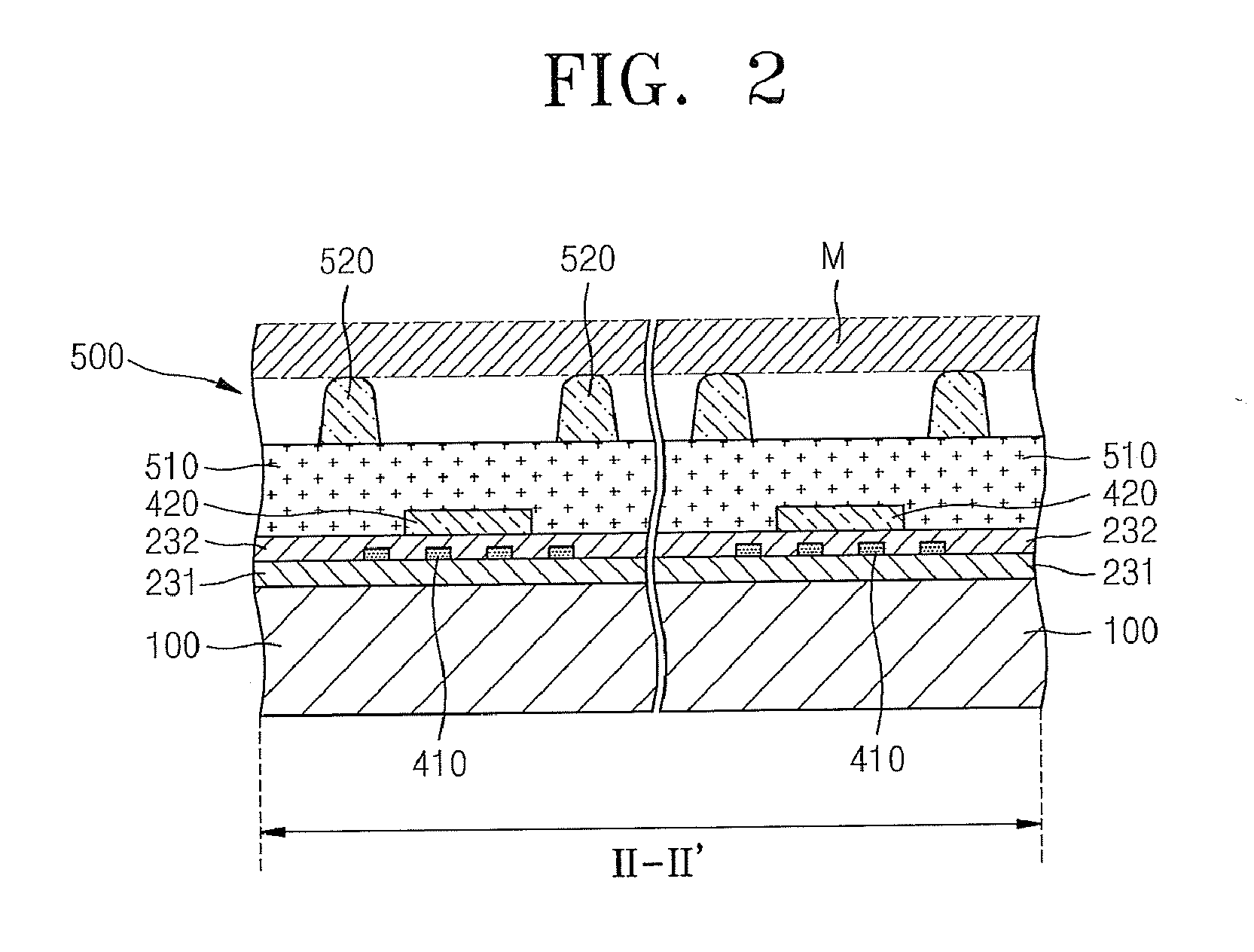
FIG. 2 is a cross-sectional view taken along the line II-II' ofFIG. 1 ; -
FIG. 3 is a cross-sectional view taken along the line III-III' ofFIG. 1 ; -
FIG. 4A is an enlarge view of area A ofFIG. 3 ; -
FIGS. 4B to 4D are schematic views illustrating various positions of the boundary line shown inFIG. 4A ; -
FIGS. 5A to 5F are cross-sectional views sequentially illustrating a process of manufacturing the organic light-emitting display apparatus shown inFIGS. 2 and 3 ; -
FIG. 6 is a cross-sectional view illustrating an organic light-emitting display apparatus according to another embodiment of the present invention; and -
FIG. 7 is a cross-sectional view illustrating an organic light-emitting display apparatus according to another embodiment of the present invention. - Reference will now be made in more detail to embodiments, examples of which are illustrated in the accompanying drawings, wherein like reference numerals refer to the like elements throughout. In this regard, the present embodiments may have different forms and should not be construed as being limited to the descriptions set forth herein. Accordingly, the embodiments are merely described below, by referring to the figures, to explain aspects of the present description. Expressions such as "at least one of," when preceding a list of elements, modify the entire list of elements and do not modify the individual elements of the list. Further, the use of "may" when describing embodiments of the present invention refers to "one or more embodiments of the present invention."
- Example embodiments of the present invention will be described below in more detail with reference to the accompanying drawings.
- Like reference numerals refer to like elements throughout. Detailed descriptions of known functions or configurations will not be repeated in order not to unnecessarily obscure the focus of the present invention.
- In the drawings, thicknesses of layers or regions may be exaggerated for clarity. Also, it will be understood that when an element, such as a layer, a film, a region, or a plate, is referred to as being 'on', 'connected to' or 'coupled to' another element, it may be directly on, connected or coupled to the other element or intervening elements may be present.
-
FIG. 1 is a plan view illustrating an organic light-emitting display apparatus according to an embodiment of the present invention.FIG. 2 is a cross-sectional view taken along the line II-II' ofFIG. 1 .FIG. 3 is a cross-sectional view taken along the line III-III' ofFIG. 1 . - Referring to
FIGS. 1 to 3 , an organic light-emitting display apparatus according to an embodiment of the present invention includes asubstrate 100; adisplay unit 200 disposed on thesubstrate 100 to display an image; and a thinfilm encapsulating layer 300 on thedisplay unit 200. The thinfilm encapsulating layer 300 is covering thedisplay unit 200. Thus, thedisplay unit 200 is interposed between thesubstrate 100 and the thinfilm encapsulating layer 300. Thedisplay unit 200 can be safely secured from permeation of moisture. Thesubstrate 100 that is used may be a substrate of a flexible material such as polyimide (PI). - A
pad unit 110 for coupling thedisplay unit 200 to a power source is disposed at one outer side (e.g., on one side outside) of thedisplay unit 200 on thesubstrate 100, and afirst wiring layer 400A with a plurality offirst wirings 410 and asecond wiring layer 400B with a plurality ofsecond wirings 420 are formed as awiring unit 400 for coupling thepad unit 110 to thedisplay unit 200. The first andsecond wirings layer 232 therebetween. Also, aprotrusion unit 500 is formed on thewiring unit 400. Since theprotrusion unit 500 supports a mask M during a deposition process for forming a thinfilm encapsulating layer 300, theprotrusion unit 500 serves to suppress or reduce the possibility of damaging thewiring unit 400 by the mask M. - For convenience of explanation, a comparative example has a structure that does not have the
protrusion unit 500, unlike the embodiment of the present invention. In this case, as described above, when the mask M is disposed to form the thinfilm encapsulating layer 300, since thesecond wiring 420 disposed on the uppermost layer directly contacts the mask M without any protective layer, damages such as scratches may occur. Also, the insulatinglayer 232 disposed between the first andsecond wirings - However, in the above-described embodiment of the present invention, the
protrusion unit 500 supports the mask M to prevent thewiring unit 400 from being damaged. That is, since theprotrusion unit 500 is erected to support the mask M so that thesecond wiring 420 disposed thereabove does not directly contact the mask M, a potential cause of a defect such as a scratch may be averted (e.g., avoided). Theprotrusion unit 500 includes a support base 510 (e.g., in the form of a strip narrower than thewiring unit 400 along the side of the display unit 200) formed on thewiring unit 400, and asupport protrusion 520 formed on thesupport base 510 to support the mask M. Also, as shown inFIG. 2 , thesupport protrusion 520 is formed on thewiring unit 400 except in a region in which thefirst wiring 410 overlaps thesecond wiring 420. Thus, the possibility of a short circuit occurring between the first andsecond wirings support protrusion 520 is, which directly supports the mask M. Thus, if the first andsecond wirings support protrusion 520, the insulatinglayer 232 may be broken and the possibility of a short circuit may increase. However, as in the structure described above, when thesupport protrusion 520 is formed on thewiring unit 400 except in the region in which thefirst wiring 410 overlaps thesecond wiring 420, even if a portion of the insulatinglayer 232 is damaged by the load, since the first andsecond wirings layer 232 is damaged by the load, contact between the first andsecond wirings - Also, the
first wiring 410 is coupled to thepad unit 110 through a contact hole. Thesecond wiring 420 is disposed flush with thepad unit 110. Here, thesecond wiring 420 extends to be a portion of thepad unit 110. Also, thesecond wiring 420 is coupled to thepad unit 110 by the other elements. - As shown in
FIG. 3 , the first andsecond wirings protrusion unit 500 are formed during a process when a thin film transistor TFT of thedisplay unit 200 and apixel 220 are formed. That is, they are not formed by a separate additional process, but are formed together when thedisplay unit 200 is formed. - Referring to
FIG. 3 , the structure of thedisplay unit 200 will be described schematically. The TFT includes anactive layer 211, agate electrode 212, asource electrode 213, and adrain electrode 214. Agate insulating layer 231 is disposed between thegate electrode 212 and theactive layer 211. Also, source and drain regions into which high density impurities are injected are formed on both edges of theactive layer 211, and are respectively coupled to the source and drainelectrodes gate electrode 212, an area between the source region and the drain region of theactive layer 211 serves as a channel to allow current to flow from thesource electrode 213 to thedrain electrode 214. - The
pixel 220 includes apixel electrode 221 coupled to thedrain electrode 214 of the TFT, anopposite electrode 223 serving as a cathode, and a light-emittinglayer 222 disposed between thepixel electrode 221 and theopposite electrode 223. Reference numeral '233' denotes a planarization layer and '234' denotes a pixel defining layer that partitions a pixel region. - Also, the positional relationship between the
wiring unit 400 and theprotrusion unit 500 is described below. Thewiring unit 400 includes a first wiring layer includes a plurality offirst wirings 410 formed on thesubstrate 100, an insulatinglayer 232 formed on thefirst wirings 410, and a second wiring layer including a plurality ofsecond wirings 420 formed on the insulatinglayer 232. Thus, thefirst wirings 410 and thesecond wirings 420 are separated by the insulatinglayer 232. A portion of thefirst wirings 410 overlap thesecond wirings 420 in the plan view inFIG. 1 . Thesupport base 510 of theprotrusion unit 500 crosses the first andsecond wirings wiring unit 400, and thesupport protrusion 520 does not overlap thesecond wirings 420 that is the uppermost layer. That is, the region where thesecond wirings 420 do not overlap thefirst wirings 410 represents a region in which thesupport protrusion 520 is formed, but not in the region in which thefirst wirings 410 overlap thesecond wirings 420, as described above. That is, when the mask M is disposed, a load is mostly applied at the point of thesupport protrusion 520 which directly supports the mask M. Since thesupport protrusion 520 is not formed in the region in which thefirst wirings 410 overlap thesecond wirings 420, even if a portion of the insulatinglayer 232 is damaged by the load, contact between thefirst wirings 410 and thesecond wirings 420 may be reduced or prevented. - Hereinafter, a process of manufacturing the organic light-emitting display apparatus having such a structure will be described.
- First, as shown in
FIG. 5A , theactive layer 211 of the TFT of thedisplay unit 200, thegate insulating layer 231, and thegate electrode 212 are sequentially formed on thesubstrate 100. Here, high density impurities are injected in both edges of theactive layer 211 to form the source and drain regions, and the source and drainelectrodes active layer 211 which is between the source region and the drain region. Also, when thegate electrode 212 is formed, thefirst wiring 410 of thewiring unit 400 is formed of the same material and on the same layer as thegate electrode 212. - Thereafter, as shown in
FIG. 5B , the insulatinglayer 232 is formed again, and then thesource electrode 213 and thedrain electrode 214 of the TFT are formed on the insulatinglayer 232. Here, a contact hole is formed (defined) in thegate insulating layer 231 and the insulatinglayer 232 to couple thesource electrode 213 to the source region of theactive layer 211 and couple thedrain electrode 214 to the drain region of theactive layer 211, respectively. Also, thesecond wiring 420 of thewiring unit 400 is formed of the same material and on the same layer as thesource electrode 213 and thedrain electrode 214. - Thereafter, as shown in
FIG. 5C , aplanarization layer 233 is formed on thedisplay unit 200, and thepixel electrode 221 of thepixel 220 is formed on theplanarization layer 233. Here, thesupport base 510 of theprotrusion unit 500 is formed of the same material and on the same layer as theplanarization layer 233 when theplanarization layer 233 is formed. - Also, as shown in
FIG. 5D , apixel defining layer 234 of thepixel 220, the light-emittinglayer 222, and anopposite electrode 223 are sequentially formed, and here, thesupport protrusion 520 of theprotrusion unit 500 is formed of the same material and on the same layer as the pixel definelayer 234 when the pixel definelayer 234 is formed, Here, thesupport protrusion 520 as described above may be formed on thewiring unit 400 except in the region in which thefirst wiring 410 overlaps thesecond wiring 420. - Next, an
inorganic layer 310 of the thinfilm encapsulating layer 300 for covering thedisplay unit 200 is formed. Here, a mask M for forming the thinfilm encapsulating layer 300 is seated (or placed) on thesupport protrusion 520 as shown inFIG. 5E . By doing so, since the mask M does not directly contact thewiring units wirings inorganic layer 310 is formed. Also, as described above, since thesupport protrusion 520 is formed on thewiring unit 400 except in the region in which thefirst wiring 410 overlaps thesecond wiring 420, even if the insulatinglayer 232 disposed below thesupport protrusion 520 is damaged by the load of the mask M, a short circuit due to contact between the first andsecond wirings inorganic layer 310 to complete the thinfilm encapsulating layer 300 as shown inFIG. 5F . An example of the stacked structure of the thinfilm encapsulating layer 300 will be described below in more detail. - When the thin
film encapsulating layer 300 is formed, since the mask M is disposed on thesupport protrusion 520, a boundary of the thinfilm encapsulating layer 300 on the pad unit-side deposited through an opening of the mask M is formed on theprotrusion unit 500. According to an embodiment of the present invention, as shown inFIG. 4A , the pad unit-side boundary L of the thinfilm encapsulating layer 300 is formed at a central position of theprotrusion unit 500. The boundary L may be alternatively formed a bit closer to thedisplay unit 200, as shown inFIG. 4B . Conversely, the boundary L may be formed a bit closer to thepad unit 110, as shown inFIG. 4C . As shown inFIG. 4D , the mask M is disposed to cover an entire top surface of theprotrusion unit 500 so that the boundary L may be formed closer to thedisplay unit 200 outside the upper surface of theprotrusion unit 500. - As described above, the thin
film encapsulating layer 300 may be formed of theinorganic layer 310 having a single layer or a multilayered structure, and may have a multilayered structure in which at least oneinorganic layer 310 and at least one organic layer are alternately stacked. Theinorganic layer 310 may have a boundary L using the mask M, and the organic layer may have a different boundary from theinorganic layer 310 by using a different mask for the organic layer. - For example, the thin
film encapsulating layer 300 may be formed as a single layer or a multilayered structure including metal oxide or metal nitride. In more detail, the inorganic layer may include at least one of SiNx, Al2O3, SiO2, or TiO2. The uppermost layer of the thinfilm encapsulating layer 300 that is exposed to the outside may be formed as an inorganic layer to prevent or reduce moisture permeation into thedisplay unit 200. Also, the thinfilm encapsulating layer 300 may include at least one sandwich structure in which at least one organic layer is inserted between at least two inorganic layers. Additionally, the thinfilm encapsulating layer 300 may include at least one sandwich structure in which at least one inorganic layer is inserted between at least two organic layers. The thinfilm encapsulating layer 300 may include a first inorganic layer, a first organic layer, and a second inorganic layer, which are sequentially stacked on thedisplay unit 200. Also, the thinfilm encapsulating layer 300 may include a first inorganic layer, a first organic layer, a second inorganic layer, a second organic layer, and a third inorganic layer, which are sequentially stacked on thedisplay unit 200. Also, the thinfilm encapsulating layer 300 may include a first inorganic layer, a first organic layer, a second inorganic layer, a second organic layer, a third inorganic layer, a third organic layer, and a fourth inorganic layer, which are sequentially stacked on thedisplay unit 200. A halogenated metal layer including LiF may be additionally included between thedisplay unit 200 and the first inorganic layer. The halogenated metal layer may prevent thedisplay unit 200 from being damaged when the first inorganic layer is formed through a sputtering method or a plasma deposition method. The first organic layer may have a narrower area than the second inorganic layer, and the second organic layer may have a narrower area than the third inorganic layer. Additionally, the first organic layer may be completely covered by the second inorganic layer. The second organic layer may be completely covered by the third inorganic layer. - The organic layer may be formed of suitable polymer materials, and may be one of polyethylene terephthalate, polyimide, polycarbonate, epoxy, polyethylene, and polyacrylate. In one embodiment, the organic layer is formed of polyacrylate. In more detail, the organic layer may include a polymerized monomer composition including diacrylate-based monomer and triacrylate-based monomer. The monomer composition may further include monoacrylate-based monomer. Moreover, the monomer composition may further include a suitable photo initiator such as TPO but is not limited thereto.
- Thus, the thin
film encapsulating layer 300 may be provided in various forms, and the mask M used here may be seated on theprotrusion unit 500 to be safely used without damaging thewiring units - Hereinafter, examples of possible modifications from the basic structure will be described. Referring to
FIG. 6 , thesupport protrusion 520 may be formed on the same layer as that of thesecond wiring 420. Here, thesupport protrusion 520 is formed on the insulatinglayer 232 except in the region in which thefirst wiring 410 overlaps thesecond wiring 420. - Also, as shown in
FIG. 7 , other examples will now be described. Like the forgoing embodiments, theprotrusion unit 500 includes thesupport base 510 and thesupport protrusion 520. Thesupport base 510 further includes aprotruding region 510a (e.g., in areas where the first and second wirings do not overlap). Also, thesupport protrusion 520 may be disposed on theprotruding region 510a of thesupport base 510. Thus, a distance between thesupport protrusion 520 and the first andsecond wirings support base 510 may be flat as in the above-described embodiments, the surface of thesupport base 510 may be changed to a shape to further include theprotruding region 510a (e.g., in areas where the first and second wirings do not overlap). Likewise, the structure may be altered in various ways. - According to the organic light-emitting display apparatus and the manufacturing method thereof as discussed above, damage to the wiring due to the mask may be effectively reduced or prevented. Thus, the product defect rate may be significantly reduced.
- It should be understood that the example embodiments described therein should be considered in a descriptive sense only and not for purposes of limitation. Descriptions of features or aspects within each embodiment should typically be considered as available for other similar features or aspects in other embodiments.
- While one or more embodiments of the present invention have been described with reference to the figures, it will be understood by those of ordinary skill in the art that various changes in form and details may be made therein without departing from the scope of the present invention as defined by the following claims.
Claims (18)
- An organic light-emitting display apparatus comprising:a display unit (200) a substrate (100);a pad unit (110) at one outer side of the display unit on the substrate;a wiring unit comprising a plurality of wiring layers (400A, 400B) on the substrate to couple the display unit to the pad unit, each of the plurality of wiring layers comprising a plurality of wirings (410, 420);a thin film encapsulating layer (300) on the display unit; anda protrusion unit (500) that does not overlap the plurality of wirings (420) of an uppermost wiring layer (400B) of the wiring unit.
- The organic light-emitting display apparatus of claim 1, wherein:the wiring unit comprises:a first wiring layer (400A) on the substrate (100);an insulating layer (232) on the first wiring layer; anda second wiring layer (400B) as the uppermost wiring layer on the insulating layer (232),and the protrusion (500) unit comprises a plurality of support protrusions (520) that do not overlap the plurality of wirings (420) of the second wiring layer (400B).
- The organic light-emitting display apparatus of claim 2, wherein:the display unit (200) comprises: a thin film transistor comprising an active layer (211), a gate electrode (212), a source electrode (213), and a drain electrode (214) that are electrically coupled;and the first wiring layer (400A) comprises a same material and is at a same layer as the gate electrode (212), and the second wiring layer (400B) comprises a same material and is at a same layer as the source electrode (213) and the drain electrode (214).
- The organic light-emitting display apparatus of claim 3, wherein:the display unit (200) further comprises:a pixel electrode (221) coupled to the drain electrode (214);an opposite electrode (223) facing the pixel electrode;a light-emitting layer (222) between the pixel electrode and the opposite electrode;a planarization layer (233) between the drain electrode and the pixel electrode; anda pixel defining layer (234) partitioning a region of the light-emitting layer (222) between the pixel electrode and the opposite electrode,wherein the support protrusions (520) comprise a same material as the pixel defining layer (234 and are on a same layer as the pixel defining layer.
- The organic light-emitting display apparatus of claim 4, wherein:the protrusion unit (500) further comprises a support base (510) on the wiring unit and supporting the support protrusions (520).
- The organic light-emitting display apparatus of claim 5, wherein:the support base (510) comprises a same material and is at a same layer as the planarization layer (223).
- The organic light-emitting display apparatus of claim 5 or 6, wherein:a top surface of the support base (510) facing the support protrusions (520) is entirely flat.
- The organic light-emitting display apparatus of claim 5 or 6, further comprising:an additional protruding region between the support protrusion (520) and the support base (510).
- The organic light-emitting display apparatus of any one of the preceding claims, wherein:the thin film encapsulating layer (300) comprises at least one inorganic layer and forms a pad unit-side boundary of the inorganic layer on the protrusion unit (500).
- The organic light-emitting display apparatus of claim 9, wherein:the thin film encapsulating layer (300) forms the pad unit-side boundary of the inorganic layer closer to the display unit (200) and outside a top surface of the protrusion unit (500).
- The organic light-emitting display apparatus of any one of the preceding claims, wherein:the thin film encapsulating layer (300) comprises at least one organic layer and at least one inorganic layer that are alternately stacked.
- The organic light-emitting display apparatus of any one of the preceding claims, wherein:the substrate (100) comprises a flexible substrate.
- A method for manufacturing an organic light-emitting display apparatus, the method comprising:forming a display unit (200) on a substrate (100);forming a pad unit (110) at one outer side of the display unit on the substrate;forming a wiring unit comprising a plurality of wiring layers (400A, 400B) to couple the display unit to the pad unit, each of the plurality of wiring layers comprising a plurality of wirings (410, 420);forming a protrusion unit (500) that does not overlap wirings (420) of an uppermost wiring layer (400B) of the wiring unit;placing a mask on the protrusion unit (500); andforming a thin film encapsulating layer (300) covering the display unit (200).
- The method of claim 13, wherein the forming of the wiring unit comprising a plurality of wiring layers comprises:forming a first wiring layer (400A) on the substrate (100);forming an insulating layer (232) on the first wiring layer (400A); andforming a second wiring layer (400B) on the insulating layer (232) as the uppermost wiring layer (400B),and the forming of the protrusion unit (500) comprises forming a support protrusion (520) for supporting the mask except in a region in which the first wiring layer (400a) overlaps the second wiring layer (400b).
- The method of claim 14, wherein the forming of the display unit (200) comprises:forming a thin film transistor comprising an active layer (211), a gate electrode (212), a source electrode (213), and a drain electrode (214) that are electrically coupled,and during the forming of the wiring unit, the first wiring layer (400A) is formed of a same material and on a same layer as the gate electrode (212), and the second wiring layer (400B) is formed of a same material and on a same layer as the source electrode (213) and the drain electrode (214).
- The method of claim 15, wherein the forming of the display unit further comprises:forming a planarization layer (233) on the thin film transistor;forming a pixel electrode (221) coupled to the drain electrode (214) on the planarization layer;forming a pixel defining layer (234) partitioning a region of a light-emitting layer (222);forming the light-emitting layer (222) on the pixel electrode; andforming an opposite electrode (223) on the light-emitting layer to face the pixel electrode,and during the forming of the protrusion unit (500), the support protrusion (520) is formed of a same material as that of the pixel defining layer (234).
- The method of claim 16, wherein:the forming of the protrusion unit (500) further comprises forming a support base (510) supporting the support protrusion (520) on the wiring unit.
- The method of claim 17, wherein:the support base (510) is formed of a same material and on a same layer as the planarization layer (233).
Applications Claiming Priority (1)
| Application Number | Priority Date | Filing Date | Title |
|---|---|---|---|
| KR20130087611 | 2013-07-24 |
Publications (3)
| Publication Number | Publication Date |
|---|---|
| EP2830095A2 true EP2830095A2 (en) | 2015-01-28 |
| EP2830095A3 EP2830095A3 (en) | 2015-04-15 |
| EP2830095B1 EP2830095B1 (en) | 2023-05-03 |
Family
ID=51212701
Family Applications (1)
| Application Number | Title | Priority Date | Filing Date |
|---|---|---|---|
| EP14177414.1A Active EP2830095B1 (en) | 2013-07-24 | 2014-07-17 | Organic light-emitting display apparatus and manufacturing method thereof |
Country Status (5)
| Country | Link |
|---|---|
| US (3) | US9614021B2 (en) |
| EP (1) | EP2830095B1 (en) |
| KR (3) | KR102210987B1 (en) |
| CN (2) | CN104347673B (en) |
| TW (2) | TWI638474B (en) |
Cited By (5)
| Publication number | Priority date | Publication date | Assignee | Title |
|---|---|---|---|---|
| CN110890400A (en) * | 2018-09-11 | 2020-03-17 | 乐金显示有限公司 | Display device |
| EP4068378A4 (en) * | 2019-11-29 | 2023-04-12 | BOE Technology Group Co., Ltd. | DISPLAY SUBSTRATE AND METHOD FOR MAKING IT, AND DISPLAY DEVICE |
| US11903256B2 (en) | 2019-11-29 | 2024-02-13 | Chengdu Boe Optoelectronics Technology Co., Ltd. | Display substrate and display device |
| US11957008B2 (en) | 2019-11-29 | 2024-04-09 | Chengdu Boe Optoelectronics Technology Co., Ltd. | Display substrate and display device |
| US12069924B2 (en) | 2019-11-29 | 2024-08-20 | Chengdu Boe Optoelectronics Technology Co., Ltd. | Display substrate and manufacturing method thereof, and display device having a plurality of apertures in a one-to-one correspondence to a plurality of first electrodes |
Families Citing this family (18)
| Publication number | Priority date | Publication date | Assignee | Title |
|---|---|---|---|---|
| US10347702B2 (en) * | 2014-10-22 | 2019-07-09 | Lg Display Co., Ltd. | Flexible thin film transistor substrate and flexible organic light emitting display device |
| KR102477299B1 (en) * | 2015-06-12 | 2022-12-14 | 삼성디스플레이 주식회사 | Display device |
| KR102465384B1 (en) | 2015-07-23 | 2022-11-10 | 삼성디스플레이 주식회사 | display apparatus |
| JP6726973B2 (en) * | 2016-02-01 | 2020-07-22 | 株式会社ジャパンディスプレイ | Display device |
| JP2017152257A (en) * | 2016-02-25 | 2017-08-31 | 株式会社ジャパンディスプレイ | Display device |
| KR102524535B1 (en) * | 2016-03-29 | 2023-04-24 | 삼성디스플레이 주식회사 | Display device |
| KR102641816B1 (en) * | 2016-07-19 | 2024-02-29 | 삼성디스플레이 주식회사 | Display apparatus |
| KR102402597B1 (en) * | 2017-10-20 | 2022-05-26 | 삼성디스플레이 주식회사 | Display device |
| KR102414940B1 (en) | 2017-10-31 | 2022-06-29 | 엘지디스플레이 주식회사 | Display device and method of manufacturing the same |
| CN108004521A (en) | 2017-11-27 | 2018-05-08 | 武汉华星光电半导体显示技术有限公司 | Mask plate and film encapsulation method |
| KR102524346B1 (en) * | 2018-01-03 | 2023-04-25 | 삼성디스플레이 주식회사 | Display device and method of manufacturing the same |
| TWI642176B (en) * | 2018-01-15 | 2018-11-21 | 友達光電股份有限公司 | Array substrate and display panel |
| KR102551354B1 (en) * | 2018-04-20 | 2023-07-04 | 삼성전자 주식회사 | Semiconductor light emitting devices and methods of manufacturing the same |
| KR20210151304A (en) | 2020-06-04 | 2021-12-14 | 삼성디스플레이 주식회사 | Display device |
| CN112909205A (en) * | 2021-02-03 | 2021-06-04 | 武汉华星光电半导体显示技术有限公司 | Display panel, preparation method thereof and display device |
| CN114975475B (en) * | 2021-02-24 | 2026-02-03 | 合肥鑫晟光电科技有限公司 | Driving backboard, manufacturing method thereof and display device |
| CN113659097B (en) * | 2021-09-13 | 2024-02-02 | 武汉天马微电子有限公司 | A display panel, a display device and a method for manufacturing a display panel |
| KR20230170192A (en) | 2022-06-09 | 2023-12-19 | 삼성디스플레이 주식회사 | Display apparatus |
Family Cites Families (31)
| Publication number | Priority date | Publication date | Assignee | Title |
|---|---|---|---|---|
| US7042024B2 (en) * | 2001-11-09 | 2006-05-09 | Semiconductor Energy Laboratory Co., Ltd. | Light emitting apparatus and method for manufacturing the same |
| US7098069B2 (en) * | 2002-01-24 | 2006-08-29 | Semiconductor Energy Laboratory Co., Ltd. | Light emitting device, method of preparing the same and device for fabricating the same |
| JP2003253434A (en) | 2002-03-01 | 2003-09-10 | Sanyo Electric Co Ltd | Vapor deposition method, and method for manufacturing display device |
| KR100551046B1 (en) * | 2003-08-28 | 2006-02-09 | 삼성에스디아이 주식회사 | Organic EL element |
| US7753751B2 (en) | 2004-09-29 | 2010-07-13 | Semiconductor Energy Laboratory Co., Ltd. | Method of fabricating the display device |
| KR100583138B1 (en) * | 2004-10-08 | 2006-05-23 | 삼성에스디아이 주식회사 | Light emitting display |
| KR20060104531A (en) * | 2005-03-30 | 2006-10-09 | 삼성에스디아이 주식회사 | Manufacturing method of light emitting display device |
| JP5376705B2 (en) * | 2005-04-28 | 2013-12-25 | 株式会社半導体エネルギー研究所 | EL display panel |
| US7710739B2 (en) | 2005-04-28 | 2010-05-04 | Semiconductor Energy Laboratory Co., Ltd. | Semiconductor device and display device |
| KR100695169B1 (en) * | 2006-01-11 | 2007-03-14 | 삼성전자주식회사 | Flat Panel Display |
| KR20070050763A (en) | 2006-06-29 | 2007-05-16 | 주식회사 대우일렉트로닉스 | Manufacturing method of ODL display device |
| KR101287215B1 (en) | 2006-11-28 | 2013-07-16 | 엘지디스플레이 주식회사 | Thin Film Transistor Array Substrate And Method For Fabricating The Same |
| KR100838082B1 (en) * | 2007-03-16 | 2008-06-16 | 삼성에스디아이 주식회사 | OLED display device and manufacturing method |
| KR100815765B1 (en) * | 2007-05-15 | 2008-03-20 | 삼성에스디아이 주식회사 | Light emitting display device and manufacturing method thereof |
| KR100897157B1 (en) * | 2008-02-28 | 2009-05-14 | 삼성모바일디스플레이주식회사 | Organic light emitting display |
| JP5478916B2 (en) * | 2008-03-14 | 2014-04-23 | 株式会社半導体エネルギー研究所 | Method for manufacturing SOI substrate |
| KR101155907B1 (en) | 2009-06-04 | 2012-06-20 | 삼성모바일디스플레이주식회사 | Organic light emitting diode display and method for manufacturing the same |
| KR101074806B1 (en) * | 2009-12-10 | 2011-10-19 | 삼성모바일디스플레이주식회사 | Organic light emitting diode display apparatus and Method thereof |
| KR101117726B1 (en) * | 2009-12-15 | 2012-03-07 | 삼성모바일디스플레이주식회사 | Substrate for flexible display device, methode for manufacturing the same, and method for manufacturing organic light emitting device |
| KR101074812B1 (en) | 2010-01-05 | 2011-10-19 | 삼성모바일디스플레이주식회사 | Organic light-emitting display device and manufacturing method of the same |
| KR101173961B1 (en) | 2010-03-24 | 2012-08-14 | (주)한 송 | Stick type mask manufacturing for big size of AMOLED multi cell panel and mask frame assembly using thereof |
| JP2011222146A (en) | 2010-04-05 | 2011-11-04 | Canon Inc | Method of manufacturing organic el display device |
| KR101745644B1 (en) * | 2010-05-28 | 2017-06-12 | 삼성디스플레이 주식회사 | Organic light emitting diode display and manufacturing method thereof |
| KR101757810B1 (en) | 2010-11-19 | 2017-07-17 | 삼성디스플레이 주식회사 | Display device, organic light emitting diode display, and manufacturing method of sealing substrate |
| KR101764272B1 (en) * | 2010-12-02 | 2017-08-16 | 삼성디스플레이 주식회사 | Organic light emitting display device and manufacturing method thereof |
| TWI516851B (en) * | 2011-05-05 | 2016-01-11 | 友達光電股份有限公司 | Lead line structure of liquid crystal display panel and liquid crystal display panel having the same |
| KR102040242B1 (en) * | 2011-05-12 | 2019-11-05 | 가부시키가이샤 한도오따이 에네루기 켄큐쇼 | Light-emitting device and electronic device using the light-emitting device |
| JP5723007B2 (en) * | 2011-07-20 | 2015-05-27 | シャープ株式会社 | Active matrix substrate and display panel having the same |
| KR101463650B1 (en) * | 2011-08-30 | 2014-11-20 | 엘지디스플레이 주식회사 | Organic Light Emitting Display Device |
| KR20130025717A (en) * | 2011-09-02 | 2013-03-12 | 삼성디스플레이 주식회사 | Organic light emitting display apparatus and method of manufacturing organic light emitting display apparatus |
| KR101900364B1 (en) * | 2011-12-22 | 2018-09-20 | 삼성디스플레이 주식회사 | Organic light emitting display apparatus and method of manufacturing the same |
-
2014
- 2014-06-02 US US14/294,101 patent/US9614021B2/en active Active
- 2014-07-17 EP EP14177414.1A patent/EP2830095B1/en active Active
- 2014-07-21 CN CN201410347304.5A patent/CN104347673B/en active Active
- 2014-07-21 KR KR1020140092082A patent/KR102210987B1/en active Active
- 2014-07-21 CN CN201811199239.0A patent/CN109390381B/en active Active
- 2014-07-22 TW TW103125195A patent/TWI638474B/en active
- 2014-07-22 TW TW107134407A patent/TWI689120B/en active
-
2017
- 2017-04-03 US US15/478,164 patent/US10431644B2/en active Active
-
2019
- 2019-08-14 US US16/540,988 patent/US11296175B2/en active Active
-
2021
- 2021-01-26 KR KR1020210011030A patent/KR102322017B1/en active Active
- 2021-10-29 KR KR1020210147162A patent/KR102367275B1/en active Active
Non-Patent Citations (1)
| Title |
|---|
| None |
Cited By (12)
| Publication number | Priority date | Publication date | Assignee | Title |
|---|---|---|---|---|
| CN110890400A (en) * | 2018-09-11 | 2020-03-17 | 乐金显示有限公司 | Display device |
| US20210225976A1 (en) | 2018-09-11 | 2021-07-22 | Lg Display Co., Ltd. | Display Device |
| CN110890400B (en) * | 2018-09-11 | 2023-09-08 | 乐金显示有限公司 | Display device |
| US11778860B2 (en) | 2018-09-11 | 2023-10-03 | Lg Display Co., Ltd. | Display device |
| US12414369B2 (en) | 2018-09-11 | 2025-09-09 | Lg Display Co., Ltd. | Display device |
| EP4068378A4 (en) * | 2019-11-29 | 2023-04-12 | BOE Technology Group Co., Ltd. | DISPLAY SUBSTRATE AND METHOD FOR MAKING IT, AND DISPLAY DEVICE |
| US11903256B2 (en) | 2019-11-29 | 2024-02-13 | Chengdu Boe Optoelectronics Technology Co., Ltd. | Display substrate and display device |
| US11957008B2 (en) | 2019-11-29 | 2024-04-09 | Chengdu Boe Optoelectronics Technology Co., Ltd. | Display substrate and display device |
| US11974473B2 (en) | 2019-11-29 | 2024-04-30 | Chengdu Boe Optoelectronics Technology Co., Ltd. | Display substrate, manufacturing method thereof and display device |
| US12069924B2 (en) | 2019-11-29 | 2024-08-20 | Chengdu Boe Optoelectronics Technology Co., Ltd. | Display substrate and manufacturing method thereof, and display device having a plurality of apertures in a one-to-one correspondence to a plurality of first electrodes |
| US12156449B2 (en) | 2019-11-29 | 2024-11-26 | Beijing Boe Technology Development Co., Ltd. | Display substrate and display device |
| US12356803B2 (en) | 2019-11-29 | 2025-07-08 | Chengdu Boe Optoelectronics Technology Co., Ltd. | Display substrate having photo spacer and pixel defining layer including a plurality of openings and display device |
Also Published As
| Publication number | Publication date |
|---|---|
| US20170207291A1 (en) | 2017-07-20 |
| KR102367275B1 (en) | 2022-02-25 |
| EP2830095A3 (en) | 2015-04-15 |
| US9614021B2 (en) | 2017-04-04 |
| TWI638474B (en) | 2018-10-11 |
| US20190371877A1 (en) | 2019-12-05 |
| TW201904106A (en) | 2019-01-16 |
| TWI689120B (en) | 2020-03-21 |
| TW201508968A (en) | 2015-03-01 |
| KR102210987B1 (en) | 2021-02-04 |
| US10431644B2 (en) | 2019-10-01 |
| CN104347673A (en) | 2015-02-11 |
| US20150028303A1 (en) | 2015-01-29 |
| EP2830095B1 (en) | 2023-05-03 |
| CN109390381A (en) | 2019-02-26 |
| KR20210013636A (en) | 2021-02-04 |
| KR20150012203A (en) | 2015-02-03 |
| CN104347673B (en) | 2018-11-09 |
| KR102322017B1 (en) | 2021-11-09 |
| US11296175B2 (en) | 2022-04-05 |
| KR20210135436A (en) | 2021-11-15 |
| CN109390381B (en) | 2023-08-29 |
Similar Documents
| Publication | Publication Date | Title |
|---|---|---|
| US11296175B2 (en) | Organic light-emitting display apparatus and manufacturing method thereof | |
| US12225757B2 (en) | Display device including a hole area for a sensor module | |
| KR102758808B1 (en) | Display device | |
| US11322564B2 (en) | Display device | |
| TWI747461B (en) | Display apparatus having substrate hole | |
| CN112117306B (en) | Display device | |
| KR102271586B1 (en) | Flexible organic light emitting device and method of menufacturing the same | |
| KR101391244B1 (en) | Organic light emitting diode display | |
| KR102082407B1 (en) | Flexible substrate, flexible display device, and method for manufacturing flexible display device | |
| CN111326548A (en) | Display device | |
| US12402494B2 (en) | Organic light-emitting display device having reduced compensated step from electrode lines to prevent cracking of encapsulation layer | |
| CN108122537B (en) | Organic Light Emitting Display Device | |
| JP2017151352A (en) | Display and flexible display | |
| JP2015173078A (en) | Organic el display device and method for manufacturing organic el display device | |
| KR20160046979A (en) | Display device | |
| KR102765792B1 (en) | Display device | |
| KR102122528B1 (en) | Flexible organic light emitting diode display device and method of fabricating the same |
Legal Events
| Date | Code | Title | Description |
|---|---|---|---|
| 17P | Request for examination filed |
Effective date: 20140717 |
|
| AK | Designated contracting states |
Kind code of ref document: A2 Designated state(s): AL AT BE BG CH CY CZ DE DK EE ES FI FR GB GR HR HU IE IS IT LI LT LU LV MC MK MT NL NO PL PT RO RS SE SI SK SM TR |
|
| AX | Request for extension of the european patent |
Extension state: BA ME |
|
| PUAI | Public reference made under article 153(3) epc to a published international application that has entered the european phase |
Free format text: ORIGINAL CODE: 0009012 |
|
| PUAL | Search report despatched |
Free format text: ORIGINAL CODE: 0009013 |
|
| RIN1 | Information on inventor provided before grant (corrected) |
Inventor name: KIM, YANG-WAN Inventor name: KWAK, WON-KYU |
|
| AK | Designated contracting states |
Kind code of ref document: A3 Designated state(s): AL AT BE BG CH CY CZ DE DK EE ES FI FR GB GR HR HU IE IS IT LI LT LU LV MC MK MT NL NO PL PT RO RS SE SI SK SM TR |
|
| AX | Request for extension of the european patent |
Extension state: BA ME |
|
| RIC1 | Information provided on ipc code assigned before grant |
Ipc: H01L 51/52 20060101ALI20150309BHEP Ipc: H01L 27/32 20060101AFI20150309BHEP Ipc: H01L 51/00 20060101ALI20150309BHEP |
|
| R17P | Request for examination filed (corrected) |
Effective date: 20150601 |
|
| RBV | Designated contracting states (corrected) |
Designated state(s): AL AT BE BG CH CY CZ DE DK EE ES FI FR GB GR HR HU IE IS IT LI LT LU LV MC MK MT NL NO PL PT RO RS SE SI SK SM TR |
|
| RAP1 | Party data changed (applicant data changed or rights of an application transferred) |
Owner name: SAMSUNG DISPLAY CO., LTD. |
|
| STAA | Information on the status of an ep patent application or granted ep patent |
Free format text: STATUS: EXAMINATION IS IN PROGRESS |
|
| 17Q | First examination report despatched |
Effective date: 20180928 |
|
| GRAP | Despatch of communication of intention to grant a patent |
Free format text: ORIGINAL CODE: EPIDOSNIGR1 |
|
| STAA | Information on the status of an ep patent application or granted ep patent |
Free format text: STATUS: GRANT OF PATENT IS INTENDED |
|
| INTG | Intention to grant announced |
Effective date: 20210112 |
|
| GRAJ | Information related to disapproval of communication of intention to grant by the applicant or resumption of examination proceedings by the epo deleted |
Free format text: ORIGINAL CODE: EPIDOSDIGR1 |
|
| STAA | Information on the status of an ep patent application or granted ep patent |
Free format text: STATUS: EXAMINATION IS IN PROGRESS |
|
| INTC | Intention to grant announced (deleted) | ||
| GRAP | Despatch of communication of intention to grant a patent |
Free format text: ORIGINAL CODE: EPIDOSNIGR1 |
|
| STAA | Information on the status of an ep patent application or granted ep patent |
Free format text: STATUS: GRANT OF PATENT IS INTENDED |
|
| RIC1 | Information provided on ipc code assigned before grant |
Ipc: H01L 51/00 20060101ALI20221024BHEP Ipc: H01L 51/52 20060101ALI20221024BHEP Ipc: H01L 27/32 20060101AFI20221024BHEP |
|
| INTG | Intention to grant announced |
Effective date: 20221111 |
|
| GRAS | Grant fee paid |
Free format text: ORIGINAL CODE: EPIDOSNIGR3 |
|
| GRAA | (expected) grant |
Free format text: ORIGINAL CODE: 0009210 |
|
| STAA | Information on the status of an ep patent application or granted ep patent |
Free format text: STATUS: THE PATENT HAS BEEN GRANTED |
|
| AK | Designated contracting states |
Kind code of ref document: B1 Designated state(s): AL AT BE BG CH CY CZ DE DK EE ES FI FR GB GR HR HU IE IS IT LI LT LU LV MC MK MT NL NO PL PT RO RS SE SI SK SM TR |
|
| REG | Reference to a national code |
Ref country code: GB Ref legal event code: FG4D |
|
| REG | Reference to a national code |
Ref country code: DE Ref legal event code: R096 Ref document number: 602014086815 Country of ref document: DE |
|
| REG | Reference to a national code |
Ref country code: AT Ref legal event code: REF Ref document number: 1565406 Country of ref document: AT Kind code of ref document: T Effective date: 20230515 Ref country code: CH Ref legal event code: EP |
|
| REG | Reference to a national code |
Ref country code: IE Ref legal event code: FG4D |
|
| P01 | Opt-out of the competence of the unified patent court (upc) registered |
Effective date: 20230515 |
|
| REG | Reference to a national code |
Ref country code: LT Ref legal event code: MG9D |
|
| REG | Reference to a national code |
Ref country code: NL Ref legal event code: MP Effective date: 20230503 |
|
| REG | Reference to a national code |
Ref country code: AT Ref legal event code: MK05 Ref document number: 1565406 Country of ref document: AT Kind code of ref document: T Effective date: 20230503 |
|
| PG25 | Lapsed in a contracting state [announced via postgrant information from national office to epo] |
Ref country code: SE Free format text: LAPSE BECAUSE OF FAILURE TO SUBMIT A TRANSLATION OF THE DESCRIPTION OR TO PAY THE FEE WITHIN THE PRESCRIBED TIME-LIMIT Effective date: 20230503 Ref country code: PT Free format text: LAPSE BECAUSE OF FAILURE TO SUBMIT A TRANSLATION OF THE DESCRIPTION OR TO PAY THE FEE WITHIN THE PRESCRIBED TIME-LIMIT Effective date: 20230904 Ref country code: NO Free format text: LAPSE BECAUSE OF FAILURE TO SUBMIT A TRANSLATION OF THE DESCRIPTION OR TO PAY THE FEE WITHIN THE PRESCRIBED TIME-LIMIT Effective date: 20230803 Ref country code: NL Free format text: LAPSE BECAUSE OF FAILURE TO SUBMIT A TRANSLATION OF THE DESCRIPTION OR TO PAY THE FEE WITHIN THE PRESCRIBED TIME-LIMIT Effective date: 20230503 Ref country code: ES Free format text: LAPSE BECAUSE OF FAILURE TO SUBMIT A TRANSLATION OF THE DESCRIPTION OR TO PAY THE FEE WITHIN THE PRESCRIBED TIME-LIMIT Effective date: 20230503 Ref country code: AT Free format text: LAPSE BECAUSE OF FAILURE TO SUBMIT A TRANSLATION OF THE DESCRIPTION OR TO PAY THE FEE WITHIN THE PRESCRIBED TIME-LIMIT Effective date: 20230503 |
|
| PG25 | Lapsed in a contracting state [announced via postgrant information from national office to epo] |
Ref country code: RS Free format text: LAPSE BECAUSE OF FAILURE TO SUBMIT A TRANSLATION OF THE DESCRIPTION OR TO PAY THE FEE WITHIN THE PRESCRIBED TIME-LIMIT Effective date: 20230503 Ref country code: PL Free format text: LAPSE BECAUSE OF FAILURE TO SUBMIT A TRANSLATION OF THE DESCRIPTION OR TO PAY THE FEE WITHIN THE PRESCRIBED TIME-LIMIT Effective date: 20230503 Ref country code: LV Free format text: LAPSE BECAUSE OF FAILURE TO SUBMIT A TRANSLATION OF THE DESCRIPTION OR TO PAY THE FEE WITHIN THE PRESCRIBED TIME-LIMIT Effective date: 20230503 Ref country code: LT Free format text: LAPSE BECAUSE OF FAILURE TO SUBMIT A TRANSLATION OF THE DESCRIPTION OR TO PAY THE FEE WITHIN THE PRESCRIBED TIME-LIMIT Effective date: 20230503 Ref country code: IS Free format text: LAPSE BECAUSE OF FAILURE TO SUBMIT A TRANSLATION OF THE DESCRIPTION OR TO PAY THE FEE WITHIN THE PRESCRIBED TIME-LIMIT Effective date: 20230903 Ref country code: HR Free format text: LAPSE BECAUSE OF FAILURE TO SUBMIT A TRANSLATION OF THE DESCRIPTION OR TO PAY THE FEE WITHIN THE PRESCRIBED TIME-LIMIT Effective date: 20230503 Ref country code: GR Free format text: LAPSE BECAUSE OF FAILURE TO SUBMIT A TRANSLATION OF THE DESCRIPTION OR TO PAY THE FEE WITHIN THE PRESCRIBED TIME-LIMIT Effective date: 20230804 |
|
| PG25 | Lapsed in a contracting state [announced via postgrant information from national office to epo] |
Ref country code: FI Free format text: LAPSE BECAUSE OF FAILURE TO SUBMIT A TRANSLATION OF THE DESCRIPTION OR TO PAY THE FEE WITHIN THE PRESCRIBED TIME-LIMIT Effective date: 20230503 |
|
| PG25 | Lapsed in a contracting state [announced via postgrant information from national office to epo] |
Ref country code: SK Free format text: LAPSE BECAUSE OF FAILURE TO SUBMIT A TRANSLATION OF THE DESCRIPTION OR TO PAY THE FEE WITHIN THE PRESCRIBED TIME-LIMIT Effective date: 20230503 |
|
| PG25 | Lapsed in a contracting state [announced via postgrant information from national office to epo] |
Ref country code: SM Free format text: LAPSE BECAUSE OF FAILURE TO SUBMIT A TRANSLATION OF THE DESCRIPTION OR TO PAY THE FEE WITHIN THE PRESCRIBED TIME-LIMIT Effective date: 20230503 Ref country code: SK Free format text: LAPSE BECAUSE OF FAILURE TO SUBMIT A TRANSLATION OF THE DESCRIPTION OR TO PAY THE FEE WITHIN THE PRESCRIBED TIME-LIMIT Effective date: 20230503 Ref country code: RO Free format text: LAPSE BECAUSE OF FAILURE TO SUBMIT A TRANSLATION OF THE DESCRIPTION OR TO PAY THE FEE WITHIN THE PRESCRIBED TIME-LIMIT Effective date: 20230503 Ref country code: EE Free format text: LAPSE BECAUSE OF FAILURE TO SUBMIT A TRANSLATION OF THE DESCRIPTION OR TO PAY THE FEE WITHIN THE PRESCRIBED TIME-LIMIT Effective date: 20230503 Ref country code: DK Free format text: LAPSE BECAUSE OF FAILURE TO SUBMIT A TRANSLATION OF THE DESCRIPTION OR TO PAY THE FEE WITHIN THE PRESCRIBED TIME-LIMIT Effective date: 20230503 Ref country code: CZ Free format text: LAPSE BECAUSE OF FAILURE TO SUBMIT A TRANSLATION OF THE DESCRIPTION OR TO PAY THE FEE WITHIN THE PRESCRIBED TIME-LIMIT Effective date: 20230503 |
|
| REG | Reference to a national code |
Ref country code: DE Ref legal event code: R097 Ref document number: 602014086815 Country of ref document: DE |
|
| PG25 | Lapsed in a contracting state [announced via postgrant information from national office to epo] |
Ref country code: MC Free format text: LAPSE BECAUSE OF FAILURE TO SUBMIT A TRANSLATION OF THE DESCRIPTION OR TO PAY THE FEE WITHIN THE PRESCRIBED TIME-LIMIT Effective date: 20230503 |
|
| PG25 | Lapsed in a contracting state [announced via postgrant information from national office to epo] |
Ref country code: MC Free format text: LAPSE BECAUSE OF FAILURE TO SUBMIT A TRANSLATION OF THE DESCRIPTION OR TO PAY THE FEE WITHIN THE PRESCRIBED TIME-LIMIT Effective date: 20230503 |
|
| REG | Reference to a national code |
Ref country code: CH Ref legal event code: PL |
|
| PLBE | No opposition filed within time limit |
Free format text: ORIGINAL CODE: 0009261 |
|
| STAA | Information on the status of an ep patent application or granted ep patent |
Free format text: STATUS: NO OPPOSITION FILED WITHIN TIME LIMIT |
|
| REG | Reference to a national code |
Ref country code: BE Ref legal event code: MM Effective date: 20230731 |
|
| PG25 | Lapsed in a contracting state [announced via postgrant information from national office to epo] |
Ref country code: LU Free format text: LAPSE BECAUSE OF NON-PAYMENT OF DUE FEES Effective date: 20230717 |
|
| PG25 | Lapsed in a contracting state [announced via postgrant information from national office to epo] |
Ref country code: LU Free format text: LAPSE BECAUSE OF NON-PAYMENT OF DUE FEES Effective date: 20230717 |
|
| 26N | No opposition filed |
Effective date: 20240206 |
|
| REG | Reference to a national code |
Ref country code: IE Ref legal event code: MM4A |
|
| PG25 | Lapsed in a contracting state [announced via postgrant information from national office to epo] |
Ref country code: CH Free format text: LAPSE BECAUSE OF NON-PAYMENT OF DUE FEES Effective date: 20230731 |
|
| PG25 | Lapsed in a contracting state [announced via postgrant information from national office to epo] |
Ref country code: SI Free format text: LAPSE BECAUSE OF FAILURE TO SUBMIT A TRANSLATION OF THE DESCRIPTION OR TO PAY THE FEE WITHIN THE PRESCRIBED TIME-LIMIT Effective date: 20230503 |
|
| PG25 | Lapsed in a contracting state [announced via postgrant information from national office to epo] |
Ref country code: SI Free format text: LAPSE BECAUSE OF FAILURE TO SUBMIT A TRANSLATION OF THE DESCRIPTION OR TO PAY THE FEE WITHIN THE PRESCRIBED TIME-LIMIT Effective date: 20230503 Ref country code: IT Free format text: LAPSE BECAUSE OF FAILURE TO SUBMIT A TRANSLATION OF THE DESCRIPTION OR TO PAY THE FEE WITHIN THE PRESCRIBED TIME-LIMIT Effective date: 20230503 Ref country code: BE Free format text: LAPSE BECAUSE OF NON-PAYMENT OF DUE FEES Effective date: 20230731 |
|
| PG25 | Lapsed in a contracting state [announced via postgrant information from national office to epo] |
Ref country code: IE Free format text: LAPSE BECAUSE OF NON-PAYMENT OF DUE FEES Effective date: 20230717 |
|
| PG25 | Lapsed in a contracting state [announced via postgrant information from national office to epo] |
Ref country code: IE Free format text: LAPSE BECAUSE OF NON-PAYMENT OF DUE FEES Effective date: 20230717 |
|
| PG25 | Lapsed in a contracting state [announced via postgrant information from national office to epo] |
Ref country code: BG Free format text: LAPSE BECAUSE OF FAILURE TO SUBMIT A TRANSLATION OF THE DESCRIPTION OR TO PAY THE FEE WITHIN THE PRESCRIBED TIME-LIMIT Effective date: 20230503 |
|
| PG25 | Lapsed in a contracting state [announced via postgrant information from national office to epo] |
Ref country code: BG Free format text: LAPSE BECAUSE OF FAILURE TO SUBMIT A TRANSLATION OF THE DESCRIPTION OR TO PAY THE FEE WITHIN THE PRESCRIBED TIME-LIMIT Effective date: 20230503 |
|
| PGFP | Annual fee paid to national office [announced via postgrant information from national office to epo] |
Ref country code: GB Payment date: 20250624 Year of fee payment: 12 |
|
| PGFP | Annual fee paid to national office [announced via postgrant information from national office to epo] |
Ref country code: FR Payment date: 20250624 Year of fee payment: 12 |
|
| PG25 | Lapsed in a contracting state [announced via postgrant information from national office to epo] |
Ref country code: CY Free format text: LAPSE BECAUSE OF FAILURE TO SUBMIT A TRANSLATION OF THE DESCRIPTION OR TO PAY THE FEE WITHIN THE PRESCRIBED TIME-LIMIT; INVALID AB INITIO Effective date: 20140717 |
|
| PG25 | Lapsed in a contracting state [announced via postgrant information from national office to epo] |
Ref country code: HU Free format text: LAPSE BECAUSE OF FAILURE TO SUBMIT A TRANSLATION OF THE DESCRIPTION OR TO PAY THE FEE WITHIN THE PRESCRIBED TIME-LIMIT; INVALID AB INITIO Effective date: 20140717 |
|
| PGFP | Annual fee paid to national office [announced via postgrant information from national office to epo] |
Ref country code: DE Payment date: 20250624 Year of fee payment: 12 |
|
| PG25 | Lapsed in a contracting state [announced via postgrant information from national office to epo] |
Ref country code: TR Free format text: LAPSE BECAUSE OF FAILURE TO SUBMIT A TRANSLATION OF THE DESCRIPTION OR TO PAY THE FEE WITHIN THE PRESCRIBED TIME-LIMIT Effective date: 20230503 |