EP2824583A1 - Bus encoding scheme based on non-uniform distribution of power delivery network components among i/o circuits - Google Patents
Bus encoding scheme based on non-uniform distribution of power delivery network components among i/o circuits Download PDFInfo
- Publication number
- EP2824583A1 EP2824583A1 EP20140171820 EP14171820A EP2824583A1 EP 2824583 A1 EP2824583 A1 EP 2824583A1 EP 20140171820 EP20140171820 EP 20140171820 EP 14171820 A EP14171820 A EP 14171820A EP 2824583 A1 EP2824583 A1 EP 2824583A1
- Authority
- EP
- European Patent Office
- Prior art keywords
- circuits
- transition
- state transitions
- subset
- requested
- Prior art date
- Legal status (The legal status is an assumption and is not a legal conclusion. Google has not performed a legal analysis and makes no representation as to the accuracy of the status listed.)
- Granted
Links
Images



Classifications
-
- H—ELECTRICITY
- H03—ELECTRONIC CIRCUITRY
- H03K—PULSE TECHNIQUE
- H03K17/00—Electronic switching or gating, i.e. not by contact-making and –breaking
- H03K17/16—Modifications for eliminating interference voltages or currents
-
- G—PHYSICS
- G06—COMPUTING OR CALCULATING; COUNTING
- G06F—ELECTRIC DIGITAL DATA PROCESSING
- G06F13/00—Interconnection of, or transfer of information or other signals between, memories, input/output devices or central processing units
- G06F13/38—Information transfer, e.g. on bus
- G06F13/42—Bus transfer protocol, e.g. handshake; Synchronisation
- G06F13/4265—Bus transfer protocol, e.g. handshake; Synchronisation on a point to point bus
-
- H—ELECTRICITY
- H03—ELECTRONIC CIRCUITRY
- H03K—PULSE TECHNIQUE
- H03K19/00—Logic circuits, i.e. having at least two inputs acting on one output; Inverting circuits
- H03K19/003—Modifications for increasing the reliability for protection
- H03K19/00346—Modifications for eliminating interference or parasitic voltages or currents
-
- G—PHYSICS
- G09—EDUCATION; CRYPTOGRAPHY; DISPLAY; ADVERTISING; SEALS
- G09G—ARRANGEMENTS OR CIRCUITS FOR CONTROL OF INDICATING DEVICES USING STATIC MEANS TO PRESENT VARIABLE INFORMATION
- G09G2330/00—Aspects of power supply; Aspects of display protection and defect management
- G09G2330/06—Handling electromagnetic interferences [EMI], covering emitted as well as received electromagnetic radiation
-
- Y—GENERAL TAGGING OF NEW TECHNOLOGICAL DEVELOPMENTS; GENERAL TAGGING OF CROSS-SECTIONAL TECHNOLOGIES SPANNING OVER SEVERAL SECTIONS OF THE IPC; TECHNICAL SUBJECTS COVERED BY FORMER USPC CROSS-REFERENCE ART COLLECTIONS [XRACs] AND DIGESTS
- Y02—TECHNOLOGIES OR APPLICATIONS FOR MITIGATION OR ADAPTATION AGAINST CLIMATE CHANGE
- Y02D—CLIMATE CHANGE MITIGATION TECHNOLOGIES IN INFORMATION AND COMMUNICATION TECHNOLOGIES [ICT], I.E. INFORMATION AND COMMUNICATION TECHNOLOGIES AIMING AT THE REDUCTION OF THEIR OWN ENERGY USE
- Y02D10/00—Energy efficient computing, e.g. low power processors, power management or thermal management
Definitions
- the invention relates to the transmission of data on a bus, and more particularly to a system and method for transmitting data with reduced simultaneous switching output (SSO) noise.
- SSO simultaneous switching output
- Buses carrying digital data on multiple parallel data lines may be used in numerous applications, e.g., for connecting integrated circuits to each other or for connecting printed wiring boards.
- a transmitter for sending data on a bus may have a plurality of input/output (I/O) circuits, one per data line, each switching the voltage on the data line between two values.
- I/O input/output
- a data line is implemented as a single conductor and a ground, e.g., as a printed wiring board (PWB) trace over a ground plane
- PWB printed wiring board
- an I/O circuit may drive the conductor with a positive voltage to signal a logical 1 (i.e., high), or with a voltage near ground to signal a logical 0 (i.e., low).
- a data line may include more than one conductor in addition to, or without, a ground conductor.
- differential signaling may be used with two conductive traces, a first trace and a second trace, over a ground plane on a PWB, and the I/O circuit may drive the first trace and the second trace in a complementary manner, so that, e.g., at any point in time, the current carried by the second trace is substantially equal in magnitude as the current carried by the first trace, and in the opposite direction.
- the I/O circuit may draw relatively high current from the power supply when it is transitioning between states, e.g., from a logical 1 to a logical 0, or vice versa.
- This current draw may cause a fluctuation in the higher power supply voltage (VDD) or the lower ground voltage (VSS) or both.
- VDD higher power supply voltage
- VSS lower ground voltage
- the fluctuation in VDD may differ in magnitude from the fluctuation in VSS. For example, if a PWB trace is used to provide VDD and a ground plane is used to provide VSS, in which case the source impedance of VDD may be greater than that of VSS, and the change in voltage resulting from an increased current draw may primarily affect VDD.
- SSO simultaneous switching output
- the magnitude of SSO noise may be reduced by installing power supply decoupling capacitances, each of which may be composed of a single capacitor or of several capacitors connected in parallel, or by increasing the number or size of the capacitors of which the power supply decoupling capacitances are composed. In some implementations, however, the space area available on the silicon, or in the package, or on the PWB for such capacitors may be limited, constraining the extent to which this mitigation technique may be used.
- SSO noise may limit an I/O interface's electrical performance, e.g., it may limit the speed at which the I/O interface may be operated. Thus, there is a need for a system and method for reducing SSO noise.
- power supply decoupling capacitances are distributed non-uniformly among a plurality of I/O circuits in a transmitter transmitting data on a bus. Transitions between consecutive values on a data bus are sent by the transmitter either as requested at the input of the transmitter, or, in cases for which the noise of the requested transition is high, converted by an encoder to transitions having lower SSO noise. The converted transitions are decoded in a receiver, so that the data at the output of the receiver are the same as the data at the input to the transmitter.
- a system for transmitting data with reduced simultaneous switching output (SSO) noise including: an encoder including a plurality of encoder inputs and a status output, the encoder inputs configured to operate in a plurality of input states, and to transition between the input states of the plurality of input states by a plurality of state transitions; and a plurality of input/output (I/O) circuits controlled by the encoder, the plurality of I/O circuits configured to operate in a plurality of I/O states, and to transition between I/O states of the plurality of I/O states by the plurality of state transitions; each I/O circuit of the plurality of I/O circuits associated with a power supply decoupling capacitance of a plurality of power supply decoupling capacitances, the decoupling capacitance of a first one of the plurality of I/O circuits being substantially smaller than the decoupling capacitance of a second one of the plurality of I/O circuit
- the converted transition is the inverse of the requested transition.
- the encoder has 2 encoder inputs and the system has 2 I/O circuits.
- the decoupling capacitance of the first one of the plurality of I/O circuits is substantially smaller than the decoupling capacitances of the others of the plurality of I/O circuits.
- the first one of the plurality of I/O circuits corresponds to the most significant bit of a data bus.
- the first subset of the plurality of transitions includes transitions in which the first one of the plurality of I/O circuits does not change state.
- the second subset of the plurality of transitions contains only: the set of transitions in which the first one of the plurality of I/O circuits changes state and at least one other I/O circuit changes state, and the transition in which the first one of the plurality of I/O circuits does not change state and all of the other I/O circuits change state.
- the system includes a receiver configured to be operatively coupled to the plurality of I/O circuits, the receiver including: a plurality of receiver inputs, each of the plurality of receiver inputs corresponding to, and configured to receive a signal from, one of the plurality of I/O circuits; and a status input operatively coupled to the status output.
- the receiver includes: a plurality of receiver outputs, each of the plurality of receiver outputs corresponding to one of the plurality of receiver inputs; and a decoder, the decoder configured to cause the receiver outputs to perform the requested transition when the plurality of receiver inputs receive a plurality of signals from the plurality of I/O circuits.
- the decoder is configured to: receive a received transition at the plurality of receiver inputs; receive, at the status input, an enable signal or a disable signal; cause the receiver outputs to perform the received transition when the status input receives a disable signal; and cause the receiver outputs to perform an alternate transition different from the received transition when the status input receives an enable signal, the alternate transition being selected to reverse a mapping, implemented in the encoder, from the requested transition to the converted transition.
- a method for transmitting data in a system including a plurality of I/O circuits, each I/O circuit of the plurality of I/O circuits associated with a power supply decoupling capacitance, the decoupling capacitance of a first one of the plurality of I/O circuits being substantially smaller than the decoupling capacitance of a second one of the plurality of I/O circuits, the method including: receiving a requested transition corresponding to a requested change in states of the I/O circuits; classifying the requested transition as being a member of: a first subset of a plurality of possible state transitions between states of the plurality of I/O circuits; or a second subset of a plurality of possible state transitions between states of the plurality of I/O circuits, the state transitions of the first subset of the plurality of possible state transitions having a lower level of SSO noise than the state transitions of the second subset of the plurality of possible state transitions, causing
- the converted transition is the inverse of the requested transition.
- the system has 4 I/O circuits.
- the decoupling capacitance of the first one of the plurality of I/O circuits is substantially smaller than the decoupling capacitance of the others of the plurality of I/O circuits.
- the first one of the plurality of I/O circuits corresponds to the most significant bit of a data bus.
- the second subset of the plurality of state transitions is the set of state transitions in which the first one of the plurality of I/O circuits changes state.
- the second subset of the plurality of state transitions contains only: the set of state transitions in which the first one of the plurality of I/O circuits changes state and at least one other I/O circuit changes state, and the state transition in which the first one of the plurality of I/O circuits does not change state and all of the other I/O circuits change state.
- a system for transmitting data with reduced simultaneous switching output (SSO) noise including: an encoder including a plurality of encoder inputs and a status output, the encoder inputs configured to operate in a plurality of input states, and to transition between the input states of the plurality of input states by a plurality of state transitions; and a plurality of input/output (I/O) circuits controlled by the encoder, the plurality of I/O circuits configured to operate in a plurality of I/O states, and to transition between I/O states of the plurality of I/O states by the plurality of state transitions; each I/O circuit of the plurality of I/O circuits associated with a power delivery network component of a plurality of power delivery network components, the power delivery network component of a first one of the plurality of I/O circuits being substantially different from the power delivery network component of a second one of the plurality of I/O circuits, each of the plurality of state transitions corresponding
- the power delivery network components include bonding wires.
- the bonding wire of a first one of the plurality of I/O circuits is substantially longer than the bonding wire of a second one of the plurality of I/O circuits.
- a plurality of I/O circuits 110 may be controlled by signals at their inputs, and may generate output signals for driving a bus.
- the bus may repeatedly transmit a parallel set of bits, each set of bits being present on the bus during an interval referred to as a time slot, and the boundaries between time slots, i.e., points in time at which a set of bits on the bus may be replaced with a new set of bits, being referred to as bus events.
- the change, or the difference between the new set of bits and the previous set of bits is referred to as a transition.
- a set of bits on the bus may be represented by a set of zeroes and ones, such as, for a four-bit bus, "0110" or "1110". Transitions may also be represented as zeroes and ones, with a one representing a change in the corresponding bit and a zero representing no change. For example, the transition between the two bit patterns "0110” and “1110” is written "1000" in this notation because the two bit patterns differ only in the first bit.
- the transition between two identical bit patterns which may occur, e.g., when the bit pattern on the bus is the same in two consecutive time slots, is referred to herein as the null transition and has (or consists of) all zeros. Given a first bit pattern and a transition it is possible to determine a second bit pattern differing from the first bit pattern by the transition; the second bit pattern may be obtained by changing the value of the first bit pattern at each position at which the transition contains a one.
- SSO noise may depend on the number of I/O circuits changing state at any given time, and also on the circuit configuration.
- a simultaneous transition from 0 to 1 in all of the I/O circuits, for example, may produce a fluctuating VDD, notionally illustrated as waveform 120.
- the magnitude of the SSO noise may depend on a number of aspects of the circuit configuration, including off-chip components 210 which may be installed between the power supply 220 and the I/O circuits 110, and which may provide power supply filtering.
- power supply decoupling capacitances such as capacitances C0, C1, Cn-2, Cn-1, may be connected across the power supply connections of the I/O circuits.
- Each power supply decoupling capacitance may be composed of a single capacitor e.g., each of the capacitors 245, or two or more capacitors, e.g., capacitors 255, 260, connected in parallel.
- the larger the value of the power supply decoupling capacitance associated with an I/O circuit the lower the resulting SSO noise contribution from that I/O circuit.
- the total SSO noise is reduced by distributing the power supply decoupling capacitances non-uniformly, i.e., by associating more or larger capacitors with one I/O circuit than with another.
- this concept is illustrated by the use of two capacitors in the power supply decoupling capacitance associated with the Bit 0 and Bit 1 I/O circuits and the use of only one capacitor in the power supply decoupling capacitance associated with the Bit n-2 and Bit n-1 I/O circuits.
- the total SSO noise may be reduced by using a bus encoding scheme which results, in some instances, in one or more of the quieter I/O circuits (i.e., those with greater power supply decoupling capacitance) making transitions instead of noisier I/O circuits (i.e., those with smaller power supply decoupling capacitance).
- the transitions may be categorized into two groups, referred to herein as A and B, the A group being ones producing higher SSO noise and the B group being ones producing lower SSO noise.
- a and B the A group being ones producing higher SSO noise
- B group the B group being ones producing lower SSO noise.
- An encoding scheme may then be used to ensure that all transitions occurring on the bus are transitions in the B group.
- the decoupling capacitance may be selected to be larger for the Bit 0 I/O circuit than for the Bit 1 I/O circuit, e.g., the capacitances may be 150 pF and 50 pF respectively.
- the most significant bit i.e., Bit 1
- changes state may produce more SSO noise than transitions in which the MSB does not change state.
- a simulation may predict that a transition in both bits may produce normalized SSO noise of 2.19, a transition in the MSB only may produce normalized SSO noise of 1.51, a transition in the least significant bit (LSB) only may produce normalized SSO noise of 0.68, and the null transition may produce normalized SSO noise of 0. If the data to be transmitted were transmitted without encoding, the worst case normalized SSO noise would be 2.19, as illustrated in the third column of FIG. 3A , entitled "SSO Noise (Normalized)".
- this worst case normalized SSO is significantly reduced by the use of encoding, resulting in the normalized SSO noise, for various transitions, shown in the fifth column of FIG. 3A , also entitled "SSO Noise (Normalized)".
- An encoder in the transmitter receives a requested transition, i.e., a requested set of data bits to be sent on the bus, which may or may not differ from the last bits sent.
- the encoder then causes the I/O circuits to perform either the requested transition, if the requested transition is in the B group, or, if the requested transition is in the A group, a converted transition, i.e., the encoder causes the I/O circuits to send the requested set of data bits, or a converted set of data bits differing from the previous set of data bits by the converted transition, where the encoding is designed so that the converted transition is in the B group.
- transitions there are four possible transitions, of which the two with higher SSO noise (shown in the third column) are in the A group, and the other two are in the B group.
- the two transitions in the A group i.e., the transitions resulting in the highest normalized SSO noise, are converted to the other two transitions, and in particular the transition "11" (corresponding to a transition in both bits) is converted to the transition "00" (corresponding to the null transition, i.e., the new data bits being the same as the previous data bits), and the transition "10" is converted to the transition "01".
- the encoder When the encoder causes the I/O circuits to perform a converted transition, instead of the requested transition, it enables a status output, which is connected to a status input on the receiver, notifying the receiver that a converted transition was used, so that the receiver may perform an alternate transition upon receipt of the transmitted data and of the status.
- the worst case normalized SSO noise is 0.68, as illustrated in the fifth column of FIG. 3A .
- the receiver is configured to reverse the encoding, for example by proceeding as follows.
- the receiver may either perform the requested transition at the receiver outputs or, if the status input is enabled, perform an alternate transition, the alternate transition selected to reverse the conversion performed in the encoder, i.e., to produce the requested transition at the receiver output.
- the SSO noise of each transition may depend only on the number of bits changing state in that transition, and the normalized SSO noise of the transition "11" may be 2.0, the normalized SSO noise of the transition "10” may be 1.0, the normalized SSO noise of the transition "01” may be 1.0, and the normalized SSO noise of the transition "00" may be 0.0.
- Encoding may substitute a low-SSO noise transition for the "11" transition, as shown in the first row of FIG. 3B resulting in a reduction of worst case normalized SSO noise from 2.0 to 1.0, a reduction that is not as great as may be achieved using a non-uniform distribution of the power supply decoupling capacitance.
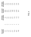
- requested transitions may be encoded to converted transitions as shown, with simulated reductions in predicted normalized SSO noise shown in the third and fifth columns respectively. Transitions having low SSO noise are not converted and are not shown in the table.
- the encoding of FIG. 4 may be used except that "1010" may be encoded to "0101" instead of to "0110” and "1001" may be encoded to "0110” instead of to "0101”; in this embodiment the encoding corresponds to inverting each bit of the transition.
- a digital display 510 such as an organic light emitting diode display or a liquid crystal display in a television or a cell phone, includes a transmitter 520 transmitting data to a receiver 530.
- the transmitter 520 is constructed to employ a bus encoding scheme based on non-uniform distribution of power delivery network components among I/O circuits, according to an embodiment of the present invention.
- the present invention may be employed to transmit data between components of a display, the invention is not thereby limited, and it may be used in other applications in which data is transmitted from a transmitter to a receiver.
- bus encoding scheme based on non-uniform distribution of power delivery network components among I/O circuits
- types of power delivery network components other than capacitors such as metal wires on the chip, bonding wires, and vias in the package, may also be used either in combination or alone, to introduce or increase the non-uniformity of SSO noise contribution among individual bus bits.
- a bus encoding scheme based on non-uniform distribution of power delivery network components among I/O circuits constructed according to principles of this invention may be embodied other than as specifically described herein.
- the invention is also defined in the following claims, and equivalents thereof.
Landscapes
- Engineering & Computer Science (AREA)
- Physics & Mathematics (AREA)
- General Engineering & Computer Science (AREA)
- Theoretical Computer Science (AREA)
- General Physics & Mathematics (AREA)
- Computer Hardware Design (AREA)
- Computing Systems (AREA)
- Mathematical Physics (AREA)
- Dc Digital Transmission (AREA)
- Design And Manufacture Of Integrated Circuits (AREA)
Abstract
Description
- The invention relates to the transmission of data on a bus, and more particularly to a system and method for transmitting data with reduced simultaneous switching output (SSO) noise.
- Buses carrying digital data on multiple parallel data lines may be used in numerous applications, e.g., for connecting integrated circuits to each other or for connecting printed wiring boards. In such an application, a transmitter for sending data on a bus may have a plurality of input/output (I/O) circuits, one per data line, each switching the voltage on the data line between two values. For example, if a data line is implemented as a single conductor and a ground, e.g., as a printed wiring board (PWB) trace over a ground plane, an I/O circuit may drive the conductor with a positive voltage to signal a logical 1 (i.e., high), or with a voltage near ground to signal a logical 0 (i.e., low). In other examples, a data line may include more than one conductor in addition to, or without, a ground conductor. For example, differential signaling may be used with two conductive traces, a first trace and a second trace, over a ground plane on a PWB, and the I/O circuit may drive the first trace and the second trace in a complementary manner, so that, e.g., at any point in time, the current carried by the second trace is substantially equal in magnitude as the current carried by the first trace, and in the opposite direction.
- The I/O circuit may draw relatively high current from the power supply when it is transitioning between states, e.g., from a logical 1 to a logical 0, or vice versa. This current draw may cause a fluctuation in the higher power supply voltage (VDD) or the lower ground voltage (VSS) or both. The fluctuation in VDD may differ in magnitude from the fluctuation in VSS. For example, if a PWB trace is used to provide VDD and a ground plane is used to provide VSS, in which case the source impedance of VDD may be greater than that of VSS, and the change in voltage resulting from an increased current draw may primarily affect VDD.
- In a synchronous system, on a bus with multiple parallel lines, several I/O circuits may, on occasion, switch simultaneously, exacerbating the fluctuations in VDD and/or VSS. This effect is referred to as simultaneous switching output (SSO) noise. The magnitude of SSO noise may be reduced by installing power supply decoupling capacitances, each of which may be composed of a single capacitor or of several capacitors connected in parallel, or by increasing the number or size of the capacitors of which the power supply decoupling capacitances are composed. In some implementations, however, the space area available on the silicon, or in the package, or on the PWB for such capacitors may be limited, constraining the extent to which this mitigation technique may be used.
- SSO noise may limit an I/O interface's electrical performance, e.g., it may limit the speed at which the I/O interface may be operated. Thus, there is a need for a system and method for reducing SSO noise.
- In one embodiment of the invention, power supply decoupling capacitances are distributed non-uniformly among a plurality of I/O circuits in a transmitter transmitting data on a bus. Transitions between consecutive values on a data bus are sent by the transmitter either as requested at the input of the transmitter, or, in cases for which the noise of the requested transition is high, converted by an encoder to transitions having lower SSO noise. The converted transitions are decoded in a receiver, so that the data at the output of the receiver are the same as the data at the input to the transmitter.
- According to an embodiment of the present invention there is provided a system for transmitting data with reduced simultaneous switching output (SSO) noise, the system including: an encoder including a plurality of encoder inputs and a status output, the encoder inputs configured to operate in a plurality of input states, and to transition between the input states of the plurality of input states by a plurality of state transitions; and a plurality of input/output (I/O) circuits controlled by the encoder, the plurality of I/O circuits configured to operate in a plurality of I/O states, and to transition between I/O states of the plurality of I/O states by the plurality of state transitions; each I/O circuit of the plurality of I/O circuits associated with a power supply decoupling capacitance of a plurality of power supply decoupling capacitances, the decoupling capacitance of a first one of the plurality of I/O circuits being substantially smaller than the decoupling capacitance of a second one of the plurality of I/O circuits, each of the plurality of state transitions corresponding to a level of SSO noise when executed by the plurality of I/O circuits, the level of SSO noise of a first subset of the plurality of state transitions being lower than the level of SSO noise of a second subset of the plurality of state transitions; the encoder configured to: receive a requested transition of the plurality of state transitions at the plurality of encoder inputs; cause the I/O circuits to perform the requested transition and disable the status output when the requested transition is one of the first subset of the plurality of state transitions; and cause the I/O circuits to perform a converted transition different from the requested transition and enable the status output when the requested transition is one of the second subset of the plurality of state transitions, the converted transition being one of the first subset of the plurality of state transitions.
- In one embodiment of the invention, the converted transition is the inverse of the requested transition.
- In one embodiment of the invention, the encoder has 2 encoder inputs and the system has 2 I/O circuits.
- In one embodiment of the invention, the decoupling capacitance of the first one of the plurality of I/O circuits is substantially smaller than the decoupling capacitances of the others of the plurality of I/O circuits.
- In one embodiment of the invention, the first one of the plurality of I/O circuits corresponds to the most significant bit of a data bus.
- In one embodiment of the invention, the first subset of the plurality of transitions includes transitions in which the first one of the plurality of I/O circuits does not change state.
- In one embodiment of the invention , the second subset of the plurality of transitions contains only: the set of transitions in which the first one of the plurality of I/O circuits changes state and at least one other I/O circuit changes state, and the transition in which the first one of the plurality of I/O circuits does not change state and all of the other I/O circuits change state.
- In one embodiment of the invention, the system includes a receiver configured to be operatively coupled to the plurality of I/O circuits, the receiver including: a plurality of receiver inputs, each of the plurality of receiver inputs corresponding to, and configured to receive a signal from, one of the plurality of I/O circuits; and a status input operatively coupled to the status output.
- In one embodiment of the invention, the receiver includes: a plurality of receiver outputs, each of the plurality of receiver outputs corresponding to one of the plurality of receiver inputs; and a decoder, the decoder configured to cause the receiver outputs to perform the requested transition when the plurality of receiver inputs receive a plurality of signals from the plurality of I/O circuits.
- In one embodiment of the invention, the decoder is configured to: receive a received transition at the plurality of receiver inputs; receive, at the status input, an enable signal or a disable signal; cause the receiver outputs to perform the received transition when the status input receives a disable signal; and cause the receiver outputs to perform an alternate transition different from the received transition when the status input receives an enable signal, the alternate transition being selected to reverse a mapping, implemented in the encoder, from the requested transition to the converted transition.
- According to an embodiment of the present invention there is provided a method for transmitting data in a system including a plurality of I/O circuits, each I/O circuit of the plurality of I/O circuits associated with a power supply decoupling capacitance, the decoupling capacitance of a first one of the plurality of I/O circuits being substantially smaller than the decoupling capacitance of a second one of the plurality of I/O circuits, the method including: receiving a requested transition corresponding to a requested change in states of the I/O circuits; classifying the requested transition as being a member of: a first subset of a plurality of possible state transitions between states of the plurality of I/O circuits; or a second subset of a plurality of possible state transitions between states of the plurality of I/O circuits, the state transitions of the first subset of the plurality of possible state transitions having a lower level of SSO noise than the state transitions of the second subset of the plurality of possible state transitions, causing the I/O circuits to perform the requested transition and disabling a status output when the requested transition is one of the first subset of the plurality of state transitions; and causing the I/O circuits to perform a converted transition different from the requested transition and enabling the status output when the requested transition is one of the second subset of the plurality of state transitions, the converted transition being one of the first subset of the plurality of state transitions.
- In one embodiment of the invention, the converted transition is the inverse of the requested transition.
- In one embodiment of the invention, the system has 4 I/O circuits.
- In one embodiment of the invention, the decoupling capacitance of the first one of the plurality of I/O circuits is substantially smaller than the decoupling capacitance of the others of the plurality of I/O circuits.
- In one embodiment of the invention, the first one of the plurality of I/O circuits corresponds to the most significant bit of a data bus.
- In one embodiment of the invention, the second subset of the plurality of state transitions is the set of state transitions in which the first one of the plurality of I/O circuits changes state.
- In one embodiment of the invention, the second subset of the plurality of state transitions contains only: the set of state transitions in which the first one of the plurality of I/O circuits changes state and at least one other I/O circuit changes state, and the state transition in which the first one of the plurality of I/O circuits does not change state and all of the other I/O circuits change state.
- According to an embodiment of the present invention there is provided a system for transmitting data with reduced simultaneous switching output (SSO) noise, the system including: an encoder including a plurality of encoder inputs and a status output, the encoder inputs configured to operate in a plurality of input states, and to transition between the input states of the plurality of input states by a plurality of state transitions; and a plurality of input/output (I/O) circuits controlled by the encoder, the plurality of I/O circuits configured to operate in a plurality of I/O states, and to transition between I/O states of the plurality of I/O states by the plurality of state transitions; each I/O circuit of the plurality of I/O circuits associated with a power delivery network component of a plurality of power delivery network components, the power delivery network component of a first one of the plurality of I/O circuits being substantially different from the power delivery network component of a second one of the plurality of I/O circuits, each of the plurality of state transitions corresponding to a level of SSO noise when executed by the plurality of I/O circuits, the level of SSO noise of a first subset of the plurality of state transitions being lower than the level of SSO noise of a second subset of the plurality of state transitions; the encoder configured to: receive a requested transition of the plurality of state transitions at the plurality of encoder inputs; cause the I/O circuits to perform the requested transition and disable the status output when the requested transition is one of the first subset of the plurality of state transitions; and cause the I/O circuits to perform a converted transition different from the requested transition and enable the status output when the requested transition is one of the second subset of the plurality of state transitions, the converted transition being one of the first subset of the plurality of state transitions.
- In one embodiment of the invention, the power delivery network components include bonding wires.
- In one embodiment of the invention, the bonding wire of a first one of the plurality of I/O circuits is substantially longer than the bonding wire of a second one of the plurality of I/O circuits.
- At least some of the above and other features of the invention wherein are set out in the claims.
- These and other features and advantages of the present invention will be appreciated and understood with reference to the description, claims and appended drawings wherein:
-
FIG. 1 is a simplified schematic diagram illustrating I/O circuits with shared power connections according to an embodiment of the present invention; -
FIG. 2 is a schematic diagram illustrating I/O circuits with non-uniform power supply decoupling capacitances according to an embodiment of the present invention; -
FIG. 3A is a table of requested transitions and encoded transitions on a two-bit bus according to an embodiment of the present invention; -
FIG. 3B is a table of requested transitions and encoded transitions according to a related art embodiment; -
FIG. 4 is a table of requested transitions and converted transitions on a four-bit bus according to an embodiment of the present invention; and -
FIG. 5 is a block diagram of a display including a transmitter and receiver constructed according to an embodiment of the present invention. - The detailed description set forth below in connection with the appended drawings is intended as a description of embodiments of a bus encoding scheme based on non-uniform distribution of power delivery network components among I/O circuits provided in accordance with the present invention and is not intended to represent the only forms in which the present invention may be constructed or utilized. The description sets forth the features of the present invention in connection with the illustrated embodiments. It is to be understood, however, that the same or equivalent functions and structures may be accomplished by different embodiments that are also intended to be encompassed within the scope of the invention. As denoted elsewhere herein, like element numbers are intended to indicate like elements or features.
- Referring to
FIG. 1 , in one embodiment, a plurality of I/O circuits 110 may be controlled by signals at their inputs, and may generate output signals for driving a bus. The bus may repeatedly transmit a parallel set of bits, each set of bits being present on the bus during an interval referred to as a time slot, and the boundaries between time slots, i.e., points in time at which a set of bits on the bus may be replaced with a new set of bits, being referred to as bus events. When a new set of bits replaces a previous set of bits on the bus, the change, or the difference between the new set of bits and the previous set of bits, is referred to as a transition. A set of bits on the bus may be represented by a set of zeroes and ones, such as, for a four-bit bus, "0110" or "1110". Transitions may also be represented as zeroes and ones, with a one representing a change in the corresponding bit and a zero representing no change. For example, the transition between the two bit patterns "0110" and "1110" is written "1000" in this notation because the two bit patterns differ only in the first bit. The transition between two identical bit patterns, which may occur, e.g., when the bit pattern on the bus is the same in two consecutive time slots, is referred to herein as the null transition and has (or consists of) all zeros. Given a first bit pattern and a transition it is possible to determine a second bit pattern differing from the first bit pattern by the transition; the second bit pattern may be obtained by changing the value of the first bit pattern at each position at which the transition contains a one. - SSO noise may depend on the number of I/O circuits changing state at any given time, and also on the circuit configuration. A simultaneous transition from 0 to 1 in all of the I/O circuits, for example, may produce a fluctuating VDD, notionally illustrated as
waveform 120. - Referring to
FIG. 2 , the magnitude of the SSO noise may depend on a number of aspects of the circuit configuration, including off-chip components 210 which may be installed between thepower supply 220 and the I/O circuits 110, and which may provide power supply filtering. In addition, power supply decoupling capacitances, such as capacitances C0, C1, Cn-2, Cn-1, may be connected across the power supply connections of the I/O circuits. Each power supply decoupling capacitance may be composed of a single capacitor e.g., each of thecapacitors 245, or two or more capacitors, e.g.,capacitors - In one embodiment, the total SSO noise is reduced by distributing the power supply decoupling capacitances non-uniformly, i.e., by associating more or larger capacitors with one I/O circuit than with another. In
FIG. 2 this concept is illustrated by the use of two capacitors in the power supply decoupling capacitance associated with theBit 0 and Bit 1 I/O circuits and the use of only one capacitor in the power supply decoupling capacitance associated with the Bit n-2 and Bit n-1 I/O circuits. In a system with a non-uniform power supply decoupling capacitance distribution of this sort, the total SSO noise may be reduced by using a bus encoding scheme which results, in some instances, in one or more of the quieter I/O circuits (i.e., those with greater power supply decoupling capacitance) making transitions instead of noisier I/O circuits (i.e., those with smaller power supply decoupling capacitance). - In a system with a non-uniform power supply decoupling capacitance distribution, numerical simulations may be used to estimate the amount of SSO noise produced by any transition, and the transitions may be categorized into two groups, referred to herein as A and B, the A group being ones producing higher SSO noise and the B group being ones producing lower SSO noise. In particular, if all of the possible transitions are ranked in order of decreasing SSO noise, the first half of the transitions form the A group, and the second half of the transitions form the B group. An encoding scheme may then be used to ensure that all transitions occurring on the bus are transitions in the B group.
- Such a scheme may be implemented as follows. Referring to
FIG. 3A , in an example bus with two data lines, i.e., a bus which transmits two bits simultaneously, the decoupling capacitance may be selected to be larger for the Bit 0 I/O circuit than for the Bit 1 I/O circuit, e.g., the capacitances may be 150 pF and 50 pF respectively. As a result, transitions in which the most significant bit (MSB), i.e.,Bit 1, changes state may produce more SSO noise than transitions in which the MSB does not change state. For example, a simulation may predict that a transition in both bits may produce normalized SSO noise of 2.19, a transition in the MSB only may produce normalized SSO noise of 1.51, a transition in the least significant bit (LSB) only may produce normalized SSO noise of 0.68, and the null transition may produce normalized SSO noise of 0. If the data to be transmitted were transmitted without encoding, the worst case normalized SSO noise would be 2.19, as illustrated in the third column ofFIG. 3A , entitled "SSO Noise (Normalized)". - In one embodiment, this worst case normalized SSO is significantly reduced by the use of encoding, resulting in the normalized SSO noise, for various transitions, shown in the fifth column of
FIG. 3A , also entitled "SSO Noise (Normalized)". An encoder in the transmitter receives a requested transition, i.e., a requested set of data bits to be sent on the bus, which may or may not differ from the last bits sent. The encoder then causes the I/O circuits to perform either the requested transition, if the requested transition is in the B group, or, if the requested transition is in the A group, a converted transition, i.e., the encoder causes the I/O circuits to send the requested set of data bits, or a converted set of data bits differing from the previous set of data bits by the converted transition, where the encoding is designed so that the converted transition is in the B group. - In the example of
FIG. 3A , there are four possible transitions, of which the two with higher SSO noise (shown in the third column) are in the A group, and the other two are in the B group. The two transitions in the A group, i.e., the transitions resulting in the highest normalized SSO noise, are converted to the other two transitions, and in particular the transition "11" (corresponding to a transition in both bits) is converted to the transition "00" (corresponding to the null transition, i.e., the new data bits being the same as the previous data bits), and the transition "10" is converted to the transition "01". When the encoder causes the I/O circuits to perform a converted transition, instead of the requested transition, it enables a status output, which is connected to a status input on the receiver, notifying the receiver that a converted transition was used, so that the receiver may perform an alternate transition upon receipt of the transmitted data and of the status. As a result of this encoding the worst case normalized SSO noise is 0.68, as illustrated in the fifth column ofFIG. 3A . - The receiver is configured to reverse the encoding, for example by proceeding as follows. Upon receiving a new set of data bits, and a received transition, the received transition being the difference between the new set of data bits and the previous set of data bits, the receiver may either perform the requested transition at the receiver outputs or, if the status input is enabled, perform an alternate transition, the alternate transition selected to reverse the conversion performed in the encoder, i.e., to produce the requested transition at the receiver output.
- By comparison, if uniform power supply decoupling capacitances were used for all of the I/O circuits, with the same total power supply decoupling capacitance, e.g., using the same PWB area for power supply decoupling capacitances, then the results of
FIG. 3B may be obtained. The SSO noise of each transition may depend only on the number of bits changing state in that transition, and the normalized SSO noise of the transition "11" may be 2.0, the normalized SSO noise of the transition "10" may be 1.0, the normalized SSO noise of the transition "01" may be 1.0, and the normalized SSO noise of the transition "00" may be 0.0. Encoding may substitute a low-SSO noise transition for the "11" transition, as shown in the first row ofFIG. 3B resulting in a reduction of worst case normalized SSO noise from 2.0 to 1.0, a reduction that is not as great as may be achieved using a non-uniform distribution of the power supply decoupling capacitance. - Referring to
FIG. 4 , in another example involving a four-bit data bus, and, correspondingly, four I/O circuits, requested transitions may be encoded to converted transitions as shown, with simulated reductions in predicted normalized SSO noise shown in the third and fifth columns respectively. Transitions having low SSO noise are not converted and are not shown in the table. In a similar embodiment, the encoding ofFIG. 4 may be used except that "1010" may be encoded to "0101" instead of to "0110" and "1001" may be encoded to "0110" instead of to "0101"; in this embodiment the encoding corresponds to inverting each bit of the transition. - Referring to
FIG. 5 , in one embodiment adigital display 510, such as an organic light emitting diode display or a liquid crystal display in a television or a cell phone, includes atransmitter 520 transmitting data to areceiver 530. Thetransmitter 520 is constructed to employ a bus encoding scheme based on non-uniform distribution of power delivery network components among I/O circuits, according to an embodiment of the present invention. Although the present invention may be employed to transmit data between components of a display, the invention is not thereby limited, and it may be used in other applications in which data is transmitted from a transmitter to a receiver. - Although embodiments of a bus encoding scheme based on non-uniform distribution of power delivery network components among I/O circuits have been specifically described and illustrated herein, many modifications and variations will be apparent to those skilled in the art. For example, types of power delivery network components other than capacitors, such as metal wires on the chip, bonding wires, and vias in the package, may also be used either in combination or alone, to introduce or increase the non-uniformity of SSO noise contribution among individual bus bits. Accordingly, it is to be understood that a bus encoding scheme based on non-uniform distribution of power delivery network components among I/O circuits constructed according to principles of this invention may be embodied other than as specifically described herein. The invention is also defined in the following claims, and equivalents thereof.
Claims (20)
- A system for transmitting data with reduced simultaneous switching output (SSO) noise, the system comprising:an encoder comprising a plurality of encoder inputs and a status output, the encoder inputs configured to operate in a plurality of input states, and to transition between the input states of the plurality of input states by a plurality of state transitions; anda plurality of input/output (I/O) circuits controlled by the encoder, the plurality of I/O circuits configured to operate in a plurality of I/O states, and to transition between I/O states of the plurality of I/O states by the plurality of state transitions;each I/O circuit of the plurality of I/O circuits associated with a power supply decoupling capacitance of a plurality of power supply decoupling capacitances, the decoupling capacitance of a first one of the plurality of I/O circuits being substantially smaller than the decoupling capacitance of a second one of the plurality of I/O circuits,each of the plurality of state transitions corresponding to a level of SSO noise when executed by the plurality of I/O circuits,the level of SSO noise of a first subset of the plurality of state transitions being lower than the level of SSO noise of a second subset of the plurality of state transitions;the encoder configured to:receive a requested transition of the plurality of state transitions at the plurality of encoder inputs;cause the I/O circuits to perform the requested transition and disable the status output when the requested transition is one of the first subset of the plurality of state transitions; andcause the I/O circuits to perform a converted transition different from the requested transition and enable the status output when the requested transition is one of the second subset of the plurality of state transitions, the converted transition being one of the first subset of the plurality of state transitions.
- A system according to claim 1, wherein the converted transition is the inverse of the requested transition.
- A system according to claim 1 or 2, wherein the encoder has 2 encoder inputs and the system has 2 I/O circuits.
- A system according to any preceding claim, wherein the decoupling capacitance of the first one of the plurality of I/O circuits is substantially smaller than the decoupling capacitances of the others of the plurality of I/O circuits.
- A system according to claim 4, wherein the first one of the plurality of I/O circuits corresponds to the most significant bit of a data bus.
- A system according to claim 4, wherein the first subset of the plurality of transitions comprises transitions in which the first one of the plurality of I/O circuits does not change state.
- A system according to claim 6, wherein the second subset of the plurality of transitions contains only:the set of transitions in which the first one of the plurality of I/O circuits changes state and at least one other I/O circuit changes state, andthe transition in which the first one of the plurality of I/O circuits does not change state and all of the other I/O circuits change state.
- A system according to any preceding claim, comprising a receiver configured to be operatively coupled to the plurality of I/O circuits, the receiver comprising:a plurality of receiver inputs, each of the plurality of receiver inputs corresponding to, and configured to receive a signal from, one of the plurality of I/O circuits; anda status input operatively coupled to the status output.
- A system according to claim 8, wherein the receiver comprises:a plurality of receiver outputs,
each of the plurality of receiver outputs corresponding to one of the plurality of receiver inputs; anda decoder,
the decoder configured to cause the receiver outputs to perform the requested transition when the plurality of receiver inputs receive a plurality of signals from the plurality of I/O circuits. - A system according to claim 9, wherein the decoder is configured to:receive a received transition at the plurality of receiver inputs;receive, at the status input, an enable signal or a disable signal;cause the receiver outputs to perform the received transition when the status input receives a disable signal; andcause the receiver outputs to perform an alternate transition different from the received transition when the status input receives an enable signal, the alternate transition being selected to reverse a mapping, implemented in the encoder, from the requested transition to the converted transition.
- A method for transmitting data in a system comprising a plurality of I/O circuits, each I/O circuit of the plurality of I/O circuits associated with a power supply decoupling capacitance, the decoupling capacitance of a first one of the plurality of I/O circuits being substantially smaller than the decoupling capacitance of a second one of the plurality of I/O circuits, the method comprising:receiving a requested transition corresponding to a requested change in states of the I/O circuits;classifying the requested transition as being a member of:a first subset of a plurality of possible state transitions between states of the plurality of I/O circuits; ora second subset of a plurality of possible state transitions between states of the plurality of I/O circuits,
the state transitions of the first subset of the plurality of possible state transitions having a lower level of SSO noise than the state transitions of the second subset of the plurality of possible state transitions,causing the I/O circuits to perform the requested transition and disabling a status output when the requested transition is one of the first subset of the plurality of state transitions; andcausing the I/O circuits to perform a converted transition different from the requested transition and enabling the status output when the requested transition is one of the second subset of the plurality of state transitions, the converted transition being one of the first subset of the plurality of state transitions. - A method according to claim 11, wherein the converted transition is the inverse of the requested transition.
- A method according to claim 12, wherein the system has 4 I/O circuits.
- A method of claim 11, 12 or 13 wherein the decoupling capacitance of the first one of the plurality of I/O circuits is substantially smaller than the decoupling capacitance of the others of the plurality of I/O circuits.
- A method according to claim 14, wherein the first one of the plurality of I/O circuits corresponds to the most significant bit of a data bus.
- A method according to claim 14, wherein the second subset of the plurality of state transitions is the set of state transitions in which the first one of the plurality of I/O circuits changes state.
- A method according to claim 14, wherein the second subset of the plurality of state transitions contains only:the set of state transitions in which the first one of the plurality of I/O circuits changes state and at least one other I/O circuit changes state, andthe state transition in which the first one of the plurality of I/O circuits does not change state and all of the other I/O circuits change state.
- A system for transmitting data with reduced simultaneous switching output (SSO) noise, the system comprising:an encoder comprising a plurality of encoder inputs and a status output, the encoder inputs configured to operate in a plurality of input states, and to transition between the input states of the plurality of input states by a plurality of state transitions; anda plurality of input/output (I/O) circuits controlled by the encoder, the plurality of I/O circuits configured to operate in a plurality of I/O states, and to transition between I/O states of the plurality of I/O states by the plurality of state transitions;each I/O circuit of the plurality of I/O circuits associated with a power delivery network component of a plurality of power delivery network components, the power delivery network component of a first one of the plurality of I/O circuits being substantially different from the power delivery network component of a second one of the plurality of I/O circuits,each of the plurality of state transitions corresponding to a level of SSO noise when executed by the plurality of I/O circuits,the level of SSO noise of a first subset of the plurality of state transitions being lower than the level of SSO noise of a second subset of the plurality of state transitions;the encoder configured to:receive a requested transition of the plurality of state transitions at the plurality of encoder inputs;cause the I/O circuits to perform the requested transition and disable the status output when the requested transition is one of the first subset of the plurality of state transitions; andcause the I/O circuits to perform a converted transition different from the requested transition and enable the status output when the requested transition is one of the second subset of the plurality of state transitions, the converted transition being one of the first subset of the plurality of state transitions.
- A system according to claim 18, wherein the power delivery network components comprise bonding wires.
- A system according to claim 19, wherein the bonding wire of a first one of the plurality of I/O circuits is substantially longer than the bonding wire of a second one of the plurality of I/O circuits.
Applications Claiming Priority (2)
| Application Number | Priority Date | Filing Date | Title |
|---|---|---|---|
| US201361845871P | 2013-07-12 | 2013-07-12 | |
| US14/174,720 US8941434B1 (en) | 2013-07-12 | 2014-02-06 | Bus encoding scheme based on non-uniform distribution of power delivery network components among I/O circuits |
Publications (2)
| Publication Number | Publication Date |
|---|---|
| EP2824583A1 true EP2824583A1 (en) | 2015-01-14 |
| EP2824583B1 EP2824583B1 (en) | 2016-10-05 |
Family
ID=50979541
Family Applications (1)
| Application Number | Title | Priority Date | Filing Date |
|---|---|---|---|
| EP14171820.5A Active EP2824583B1 (en) | 2013-07-12 | 2014-06-10 | Bus encoding scheme based on non-uniform distribution of power delivery network components among i/o circuits |
Country Status (3)
| Country | Link |
|---|---|
| US (1) | US8941434B1 (en) |
| EP (1) | EP2824583B1 (en) |
| CN (1) | CN104282272B (en) |
Families Citing this family (1)
| Publication number | Priority date | Publication date | Assignee | Title |
|---|---|---|---|---|
| US12218694B2 (en) * | 2023-04-05 | 2025-02-04 | Schweitzer Engineering Laboratories, Inc. | Bit pattern sequence compressor |
Citations (3)
| Publication number | Priority date | Publication date | Assignee | Title |
|---|---|---|---|---|
| US20010004227A1 (en) * | 1999-12-16 | 2001-06-21 | Roland Frech | Tunable on-chip capacity |
| US20100052765A1 (en) * | 2008-09-03 | 2010-03-04 | Nec Electronics Corporation | Semiconductor integrated circuit and method of leveling switching noise thereof |
| US20120229310A1 (en) * | 2011-03-11 | 2012-09-13 | Taiwan Semiconductor Manufacturing Company, Ltd. | Using Bus Inversion to Reduce Simultaneous Signal Switching |
Family Cites Families (19)
| Publication number | Priority date | Publication date | Assignee | Title |
|---|---|---|---|---|
| DE19525019A1 (en) * | 1995-06-28 | 1997-01-02 | Dietmar Dipl Ing Hennig | Matrix circuit for multiplexed displays and drive circuits |
| JP4695770B2 (en) * | 2001-03-28 | 2011-06-08 | パナソニック株式会社 | Plasma display device |
| KR100429871B1 (en) * | 2001-06-07 | 2004-05-04 | 삼성전자주식회사 | Semiconductor device having a plurality of output signals |
| US6653857B2 (en) * | 2001-10-31 | 2003-11-25 | Sun Microsystems, Inc. | Increasing implicit decoupling capacitance using asymmetric shieldings |
| US6628138B2 (en) * | 2001-11-30 | 2003-09-30 | Sun Microsystems, Inc. | Increasing decoupling capacitance using preferential shields |
| KR100611506B1 (en) | 2004-06-18 | 2006-08-11 | 삼성전자주식회사 | Decoupling capacitance control circuit of semiconductor memory device |
| KR100592787B1 (en) | 2004-11-09 | 2006-06-26 | 삼성전자주식회사 | Integrated Circuit Chip Package with Ring-Shaped Silicon Decoupling Capacitors |
| US7778038B2 (en) * | 2004-12-21 | 2010-08-17 | E.I. Du Pont De Nemours And Company | Power core devices and methods of making thereof |
| JP2007234857A (en) * | 2006-03-01 | 2007-09-13 | Matsushita Electric Ind Co Ltd | Semiconductor integrated circuit and design method of semiconductor integrated circuit |
| US7600208B1 (en) * | 2007-01-31 | 2009-10-06 | Cadence Design Systems, Inc. | Automatic placement of decoupling capacitors |
| KR100849957B1 (en) * | 2007-03-08 | 2008-08-01 | 삼성전자주식회사 | Semiconductor memory device and its input / output driving circuit and current supply method thereof |
| US7818704B1 (en) * | 2007-05-16 | 2010-10-19 | Altera Corporation | Capacitive decoupling method and module |
| US7616133B2 (en) * | 2008-01-16 | 2009-11-10 | Micron Technology, Inc. | Data bus inversion apparatus, systems, and methods |
| JP2009246062A (en) * | 2008-03-31 | 2009-10-22 | Hitachi Ltd | Semiconductor integrated circuit apparatus and method of manufacturing the same |
| JP4605550B2 (en) * | 2008-10-09 | 2011-01-05 | 日本電気株式会社 | Capacitor placement method |
| KR20100084379A (en) | 2009-01-16 | 2010-07-26 | 삼성전자주식회사 | Printed circuit board |
| JP5731759B2 (en) * | 2010-04-23 | 2015-06-10 | ルネサスエレクトロニクス株式会社 | Decoupling circuit and semiconductor integrated circuit |
| US8610188B2 (en) * | 2011-09-15 | 2013-12-17 | GlobalFoundries, Inc. | Integrated circuit decoupling capacitor arrangement |
| CN102521190A (en) * | 2011-12-19 | 2012-06-27 | 中国科学院自动化研究所 | Hierarchical bus system applied to real-time data processing |
-
2014
- 2014-02-06 US US14/174,720 patent/US8941434B1/en not_active Expired - Fee Related
- 2014-06-10 EP EP14171820.5A patent/EP2824583B1/en active Active
- 2014-07-04 CN CN201410317509.9A patent/CN104282272B/en active Active
Patent Citations (3)
| Publication number | Priority date | Publication date | Assignee | Title |
|---|---|---|---|---|
| US20010004227A1 (en) * | 1999-12-16 | 2001-06-21 | Roland Frech | Tunable on-chip capacity |
| US20100052765A1 (en) * | 2008-09-03 | 2010-03-04 | Nec Electronics Corporation | Semiconductor integrated circuit and method of leveling switching noise thereof |
| US20120229310A1 (en) * | 2011-03-11 | 2012-09-13 | Taiwan Semiconductor Manufacturing Company, Ltd. | Using Bus Inversion to Reduce Simultaneous Signal Switching |
Also Published As
| Publication number | Publication date |
|---|---|
| CN104282272B (en) | 2018-04-24 |
| US20150015320A1 (en) | 2015-01-15 |
| US8941434B1 (en) | 2015-01-27 |
| CN104282272A (en) | 2015-01-14 |
| EP2824583B1 (en) | 2016-10-05 |
Similar Documents
| Publication | Publication Date | Title |
|---|---|---|
| JP6126317B1 (en) | Encoding for partitioned data bus | |
| US7339502B2 (en) | Method and device for transmitting data over a plurality of transmission lines | |
| US7781677B2 (en) | Transmission cable | |
| CN104133799A (en) | Multi-network-card NCSI management system | |
| CN104808966A (en) | Method and apparatus for valid encoding | |
| EP2824583B1 (en) | Bus encoding scheme based on non-uniform distribution of power delivery network components among i/o circuits | |
| CN105791850B (en) | A kind of encoder and its coding method, decoder and its coding/decoding method | |
| CN114302554B (en) | PCB (printed circuit board) capable of improving integrity of cross-split signals based on capacitance and layout method thereof | |
| CN204009884U (en) | A kind of many network interface cards NCSI management system | |
| US11588666B2 (en) | Signal transmission system, transmitter encoding apparatus and receiver decoding apparatus | |
| US8179158B2 (en) | Printed circuit board having a termination of a T-shaped signal line | |
| KR102034369B1 (en) | Transmitter capable of transmitting clock with removing simultaneous switching noise and data and method of operating the same | |
| WO2015157627A1 (en) | Systems and methods for frequency control on a bus through superposition | |
| US20130258630A1 (en) | Hard disk drive connector | |
| US9542305B2 (en) | Impedance matching for high speed signaling in memory system | |
| KR101249833B1 (en) | Pcb with low emi noise | |
| US8456457B2 (en) | Printed circuit board | |
| CN208315205U (en) | A kind of circuit of compatible multiple interfaces SSD | |
| CN223362623U (en) | A one-master-multiple-slave serial peripheral interface bus circuit | |
| KR102126425B1 (en) | Data processing apparatus and method for processing data | |
| US9069913B2 (en) | Circuit topology for multiple loads | |
| JP2010268180A (en) | Digital signal transmission system, transmitter and receiver | |
| US20170052923A1 (en) | Apparatuses and methods for balanced transmittal of data | |
| CN108665930B (en) | A NAND flash memory chip | |
| Huh et al. | Design of power delivery networks using power transmission lines and pseudo-balanced signaling for multiple I/Os |
Legal Events
| Date | Code | Title | Description |
|---|---|---|---|
| 17P | Request for examination filed |
Effective date: 20140610 |
|
| AK | Designated contracting states |
Kind code of ref document: A1 Designated state(s): AL AT BE BG CH CY CZ DE DK EE ES FI FR GB GR HR HU IE IS IT LI LT LU LV MC MK MT NL NO PL PT RO RS SE SI SK SM TR |
|
| AX | Request for extension of the european patent |
Extension state: BA ME |
|
| PUAI | Public reference made under article 153(3) epc to a published international application that has entered the european phase |
Free format text: ORIGINAL CODE: 0009012 |
|
| R17P | Request for examination filed (corrected) |
Effective date: 20150713 |
|
| RBV | Designated contracting states (corrected) |
Designated state(s): AL AT BE BG CH CY CZ DE DK EE ES FI FR GB GR HR HU IE IS IT LI LT LU LV MC MK MT NL NO PL PT RO RS SE SI SK SM TR |
|
| RAP1 | Party data changed (applicant data changed or rights of an application transferred) |
Owner name: SAMSUNG DISPLAY CO., LTD. |
|
| GRAP | Despatch of communication of intention to grant a patent |
Free format text: ORIGINAL CODE: EPIDOSNIGR1 |
|
| INTG | Intention to grant announced |
Effective date: 20160419 |
|
| GRAS | Grant fee paid |
Free format text: ORIGINAL CODE: EPIDOSNIGR3 |
|
| GRAA | (expected) grant |
Free format text: ORIGINAL CODE: 0009210 |
|
| AK | Designated contracting states |
Kind code of ref document: B1 Designated state(s): AL AT BE BG CH CY CZ DE DK EE ES FI FR GB GR HR HU IE IS IT LI LT LU LV MC MK MT NL NO PL PT RO RS SE SI SK SM TR |
|
| REG | Reference to a national code |
Ref country code: GB Ref legal event code: FG4D |
|
| REG | Reference to a national code |
Ref country code: CH Ref legal event code: EP |
|
| REG | Reference to a national code |
Ref country code: AT Ref legal event code: REF Ref document number: 835172 Country of ref document: AT Kind code of ref document: T Effective date: 20161015 |
|
| REG | Reference to a national code |
Ref country code: IE Ref legal event code: FG4D |
|
| REG | Reference to a national code |
Ref country code: DE Ref legal event code: R096 Ref document number: 602014004043 Country of ref document: DE |
|
| REG | Reference to a national code |
Ref country code: NL Ref legal event code: MP Effective date: 20161005 |
|
| REG | Reference to a national code |
Ref country code: LT Ref legal event code: MG4D |
|
| PG25 | Lapsed in a contracting state [announced via postgrant information from national office to epo] |
Ref country code: LV Free format text: LAPSE BECAUSE OF FAILURE TO SUBMIT A TRANSLATION OF THE DESCRIPTION OR TO PAY THE FEE WITHIN THE PRESCRIBED TIME-LIMIT Effective date: 20161005 |
|
| REG | Reference to a national code |
Ref country code: AT Ref legal event code: MK05 Ref document number: 835172 Country of ref document: AT Kind code of ref document: T Effective date: 20161005 |
|
| PG25 | Lapsed in a contracting state [announced via postgrant information from national office to epo] |
Ref country code: LT Free format text: LAPSE BECAUSE OF FAILURE TO SUBMIT A TRANSLATION OF THE DESCRIPTION OR TO PAY THE FEE WITHIN THE PRESCRIBED TIME-LIMIT Effective date: 20161005 Ref country code: NO Free format text: LAPSE BECAUSE OF FAILURE TO SUBMIT A TRANSLATION OF THE DESCRIPTION OR TO PAY THE FEE WITHIN THE PRESCRIBED TIME-LIMIT Effective date: 20170105 Ref country code: GR Free format text: LAPSE BECAUSE OF FAILURE TO SUBMIT A TRANSLATION OF THE DESCRIPTION OR TO PAY THE FEE WITHIN THE PRESCRIBED TIME-LIMIT Effective date: 20170106 Ref country code: SE Free format text: LAPSE BECAUSE OF FAILURE TO SUBMIT A TRANSLATION OF THE DESCRIPTION OR TO PAY THE FEE WITHIN THE PRESCRIBED TIME-LIMIT Effective date: 20161005 |
|
| PG25 | Lapsed in a contracting state [announced via postgrant information from national office to epo] |
Ref country code: PT Free format text: LAPSE BECAUSE OF FAILURE TO SUBMIT A TRANSLATION OF THE DESCRIPTION OR TO PAY THE FEE WITHIN THE PRESCRIBED TIME-LIMIT Effective date: 20170206 Ref country code: HR Free format text: LAPSE BECAUSE OF FAILURE TO SUBMIT A TRANSLATION OF THE DESCRIPTION OR TO PAY THE FEE WITHIN THE PRESCRIBED TIME-LIMIT Effective date: 20161005 Ref country code: NL Free format text: LAPSE BECAUSE OF FAILURE TO SUBMIT A TRANSLATION OF THE DESCRIPTION OR TO PAY THE FEE WITHIN THE PRESCRIBED TIME-LIMIT Effective date: 20161005 Ref country code: BE Free format text: LAPSE BECAUSE OF FAILURE TO SUBMIT A TRANSLATION OF THE DESCRIPTION OR TO PAY THE FEE WITHIN THE PRESCRIBED TIME-LIMIT Effective date: 20161005 Ref country code: FI Free format text: LAPSE BECAUSE OF FAILURE TO SUBMIT A TRANSLATION OF THE DESCRIPTION OR TO PAY THE FEE WITHIN THE PRESCRIBED TIME-LIMIT Effective date: 20161005 Ref country code: PL Free format text: LAPSE BECAUSE OF FAILURE TO SUBMIT A TRANSLATION OF THE DESCRIPTION OR TO PAY THE FEE WITHIN THE PRESCRIBED TIME-LIMIT Effective date: 20161005 Ref country code: AT Free format text: LAPSE BECAUSE OF FAILURE TO SUBMIT A TRANSLATION OF THE DESCRIPTION OR TO PAY THE FEE WITHIN THE PRESCRIBED TIME-LIMIT Effective date: 20161005 Ref country code: RS Free format text: LAPSE BECAUSE OF FAILURE TO SUBMIT A TRANSLATION OF THE DESCRIPTION OR TO PAY THE FEE WITHIN THE PRESCRIBED TIME-LIMIT Effective date: 20161005 Ref country code: ES Free format text: LAPSE BECAUSE OF FAILURE TO SUBMIT A TRANSLATION OF THE DESCRIPTION OR TO PAY THE FEE WITHIN THE PRESCRIBED TIME-LIMIT Effective date: 20161005 Ref country code: IS Free format text: LAPSE BECAUSE OF FAILURE TO SUBMIT A TRANSLATION OF THE DESCRIPTION OR TO PAY THE FEE WITHIN THE PRESCRIBED TIME-LIMIT Effective date: 20170205 |
|
| REG | Reference to a national code |
Ref country code: FR Ref legal event code: PLFP Year of fee payment: 4 |
|
| REG | Reference to a national code |
Ref country code: DE Ref legal event code: R097 Ref document number: 602014004043 Country of ref document: DE |
|
| PG25 | Lapsed in a contracting state [announced via postgrant information from national office to epo] |
Ref country code: SK Free format text: LAPSE BECAUSE OF FAILURE TO SUBMIT A TRANSLATION OF THE DESCRIPTION OR TO PAY THE FEE WITHIN THE PRESCRIBED TIME-LIMIT Effective date: 20161005 Ref country code: CZ Free format text: LAPSE BECAUSE OF FAILURE TO SUBMIT A TRANSLATION OF THE DESCRIPTION OR TO PAY THE FEE WITHIN THE PRESCRIBED TIME-LIMIT Effective date: 20161005 Ref country code: DK Free format text: LAPSE BECAUSE OF FAILURE TO SUBMIT A TRANSLATION OF THE DESCRIPTION OR TO PAY THE FEE WITHIN THE PRESCRIBED TIME-LIMIT Effective date: 20161005 Ref country code: EE Free format text: LAPSE BECAUSE OF FAILURE TO SUBMIT A TRANSLATION OF THE DESCRIPTION OR TO PAY THE FEE WITHIN THE PRESCRIBED TIME-LIMIT Effective date: 20161005 Ref country code: RO Free format text: LAPSE BECAUSE OF FAILURE TO SUBMIT A TRANSLATION OF THE DESCRIPTION OR TO PAY THE FEE WITHIN THE PRESCRIBED TIME-LIMIT Effective date: 20161005 |
|
| PLBE | No opposition filed within time limit |
Free format text: ORIGINAL CODE: 0009261 |
|
| STAA | Information on the status of an ep patent application or granted ep patent |
Free format text: STATUS: NO OPPOSITION FILED WITHIN TIME LIMIT |
|
| PG25 | Lapsed in a contracting state [announced via postgrant information from national office to epo] |
Ref country code: BG Free format text: LAPSE BECAUSE OF FAILURE TO SUBMIT A TRANSLATION OF THE DESCRIPTION OR TO PAY THE FEE WITHIN THE PRESCRIBED TIME-LIMIT Effective date: 20170105 Ref country code: SM Free format text: LAPSE BECAUSE OF FAILURE TO SUBMIT A TRANSLATION OF THE DESCRIPTION OR TO PAY THE FEE WITHIN THE PRESCRIBED TIME-LIMIT Effective date: 20161005 Ref country code: IT Free format text: LAPSE BECAUSE OF FAILURE TO SUBMIT A TRANSLATION OF THE DESCRIPTION OR TO PAY THE FEE WITHIN THE PRESCRIBED TIME-LIMIT Effective date: 20161005 |
|
| 26N | No opposition filed |
Effective date: 20170706 |
|
| PG25 | Lapsed in a contracting state [announced via postgrant information from national office to epo] |
Ref country code: SI Free format text: LAPSE BECAUSE OF FAILURE TO SUBMIT A TRANSLATION OF THE DESCRIPTION OR TO PAY THE FEE WITHIN THE PRESCRIBED TIME-LIMIT Effective date: 20161005 |
|
| PG25 | Lapsed in a contracting state [announced via postgrant information from national office to epo] |
Ref country code: MC Free format text: LAPSE BECAUSE OF FAILURE TO SUBMIT A TRANSLATION OF THE DESCRIPTION OR TO PAY THE FEE WITHIN THE PRESCRIBED TIME-LIMIT Effective date: 20161005 |
|
| REG | Reference to a national code |
Ref country code: CH Ref legal event code: PL |
|
| REG | Reference to a national code |
Ref country code: IE Ref legal event code: MM4A |
|
| PG25 | Lapsed in a contracting state [announced via postgrant information from national office to epo] |
Ref country code: LI Free format text: LAPSE BECAUSE OF NON-PAYMENT OF DUE FEES Effective date: 20170630 Ref country code: CH Free format text: LAPSE BECAUSE OF NON-PAYMENT OF DUE FEES Effective date: 20170630 Ref country code: IE Free format text: LAPSE BECAUSE OF NON-PAYMENT OF DUE FEES Effective date: 20170610 Ref country code: LU Free format text: LAPSE BECAUSE OF NON-PAYMENT OF DUE FEES Effective date: 20170610 |
|
| REG | Reference to a national code |
Ref country code: FR Ref legal event code: PLFP Year of fee payment: 5 |
|
| PG25 | Lapsed in a contracting state [announced via postgrant information from national office to epo] |
Ref country code: MT Free format text: LAPSE BECAUSE OF NON-PAYMENT OF DUE FEES Effective date: 20170610 |
|
| PG25 | Lapsed in a contracting state [announced via postgrant information from national office to epo] |
Ref country code: HU Free format text: LAPSE BECAUSE OF FAILURE TO SUBMIT A TRANSLATION OF THE DESCRIPTION OR TO PAY THE FEE WITHIN THE PRESCRIBED TIME-LIMIT; INVALID AB INITIO Effective date: 20140610 |
|
| PG25 | Lapsed in a contracting state [announced via postgrant information from national office to epo] |
Ref country code: CY Free format text: LAPSE BECAUSE OF FAILURE TO SUBMIT A TRANSLATION OF THE DESCRIPTION OR TO PAY THE FEE WITHIN THE PRESCRIBED TIME-LIMIT Effective date: 20161005 |
|
| PG25 | Lapsed in a contracting state [announced via postgrant information from national office to epo] |
Ref country code: MK Free format text: LAPSE BECAUSE OF FAILURE TO SUBMIT A TRANSLATION OF THE DESCRIPTION OR TO PAY THE FEE WITHIN THE PRESCRIBED TIME-LIMIT Effective date: 20161005 |
|
| PG25 | Lapsed in a contracting state [announced via postgrant information from national office to epo] |
Ref country code: TR Free format text: LAPSE BECAUSE OF FAILURE TO SUBMIT A TRANSLATION OF THE DESCRIPTION OR TO PAY THE FEE WITHIN THE PRESCRIBED TIME-LIMIT Effective date: 20161005 |
|
| PG25 | Lapsed in a contracting state [announced via postgrant information from national office to epo] |
Ref country code: AL Free format text: LAPSE BECAUSE OF FAILURE TO SUBMIT A TRANSLATION OF THE DESCRIPTION OR TO PAY THE FEE WITHIN THE PRESCRIBED TIME-LIMIT Effective date: 20161005 |
|
| P01 | Opt-out of the competence of the unified patent court (upc) registered |
Effective date: 20230516 |
|
| PGFP | Annual fee paid to national office [announced via postgrant information from national office to epo] |
Ref country code: DE Payment date: 20250520 Year of fee payment: 12 |
|
| PGFP | Annual fee paid to national office [announced via postgrant information from national office to epo] |
Ref country code: GB Payment date: 20250520 Year of fee payment: 12 |
|
| PGFP | Annual fee paid to national office [announced via postgrant information from national office to epo] |
Ref country code: FR Payment date: 20250521 Year of fee payment: 12 |