EP2822269A1 - Image sensor, imaging system, sensor, and operation method for image sensor - Google Patents
Image sensor, imaging system, sensor, and operation method for image sensor Download PDFInfo
- Publication number
- EP2822269A1 EP2822269A1 EP14172276.9A EP14172276A EP2822269A1 EP 2822269 A1 EP2822269 A1 EP 2822269A1 EP 14172276 A EP14172276 A EP 14172276A EP 2822269 A1 EP2822269 A1 EP 2822269A1
- Authority
- EP
- European Patent Office
- Prior art keywords
- row
- column
- signal
- output
- horizontal
- Prior art date
- Legal status (The legal status is an assumption and is not a legal conclusion. Google has not performed a legal analysis and makes no representation as to the accuracy of the status listed.)
- Withdrawn
Links
Images


Classifications
-
- H—ELECTRICITY
- H04—ELECTRIC COMMUNICATION TECHNIQUE
- H04N—PICTORIAL COMMUNICATION, e.g. TELEVISION
- H04N25/00—Circuitry of solid-state image sensors [SSIS]; Control thereof
- H04N25/70—SSIS architectures; Circuits associated therewith
- H04N25/76—Addressed sensors, e.g. MOS or CMOS sensors
- H04N25/779—Circuitry for scanning or addressing the pixel array
-
- H—ELECTRICITY
- H04—ELECTRIC COMMUNICATION TECHNIQUE
- H04N—PICTORIAL COMMUNICATION, e.g. TELEVISION
- H04N25/00—Circuitry of solid-state image sensors [SSIS]; Control thereof
- H04N25/60—Noise processing, e.g. detecting, correcting, reducing or removing noise
- H04N25/67—Noise processing, e.g. detecting, correcting, reducing or removing noise applied to fixed-pattern noise, e.g. non-uniformity of response
- H04N25/671—Noise processing, e.g. detecting, correcting, reducing or removing noise applied to fixed-pattern noise, e.g. non-uniformity of response for non-uniformity detection or correction
- H04N25/677—Noise processing, e.g. detecting, correcting, reducing or removing noise applied to fixed-pattern noise, e.g. non-uniformity of response for non-uniformity detection or correction for reducing the column or line fixed pattern noise
-
- H—ELECTRICITY
- H04—ELECTRIC COMMUNICATION TECHNIQUE
- H04N—PICTORIAL COMMUNICATION, e.g. TELEVISION
- H04N25/00—Circuitry of solid-state image sensors [SSIS]; Control thereof
- H04N25/70—SSIS architectures; Circuits associated therewith
- H04N25/76—Addressed sensors, e.g. MOS or CMOS sensors
- H04N25/767—Horizontal readout lines, multiplexers or registers
-
- H—ELECTRICITY
- H04—ELECTRIC COMMUNICATION TECHNIQUE
- H04N—PICTORIAL COMMUNICATION, e.g. TELEVISION
- H04N25/00—Circuitry of solid-state image sensors [SSIS]; Control thereof
- H04N25/70—SSIS architectures; Circuits associated therewith
- H04N25/76—Addressed sensors, e.g. MOS or CMOS sensors
- H04N25/7795—Circuitry for generating timing or clock signals
-
- H—ELECTRICITY
- H04—ELECTRIC COMMUNICATION TECHNIQUE
- H04N—PICTORIAL COMMUNICATION, e.g. TELEVISION
- H04N25/00—Circuitry of solid-state image sensors [SSIS]; Control thereof
- H04N25/70—SSIS architectures; Circuits associated therewith
- H04N25/76—Addressed sensors, e.g. MOS or CMOS sensors
- H04N25/78—Readout circuits for addressed sensors, e.g. output amplifiers or A/D converters
Definitions
- the present invention relates to an image sensor, an imaging system, a sensor, and an operation method for the image sensor.
- a row selecting circuit selects a row of a pixel array, and a plurality of pixels on the selected row output signals to a plurality of column signal lines.
- a column selecting circuit then outputs signals from the pixels on one row while sequentially selecting a plurality of column signal lines.
- the image sensor sequentially performs this operation for a plurality of rows while changing a row to be selected.
- a readout period for signals is constant regardless of any row selected from a plurality of rows of a pixel array.
- the present invention provides a technique advantageous to reduce shading due shortages of readout period corresponding to row positions.
- a first aspect of the present invention provides an image sensor specified in claims 1 to 10.
- a second aspect of the present invention provides an imaging system specified in claim 11.
- a third aspect of the present invention provides a sensor specified in claims 12 to 14.
- a fourth aspect of the present invention provides an operation method for an image sensor specified in claim 15.
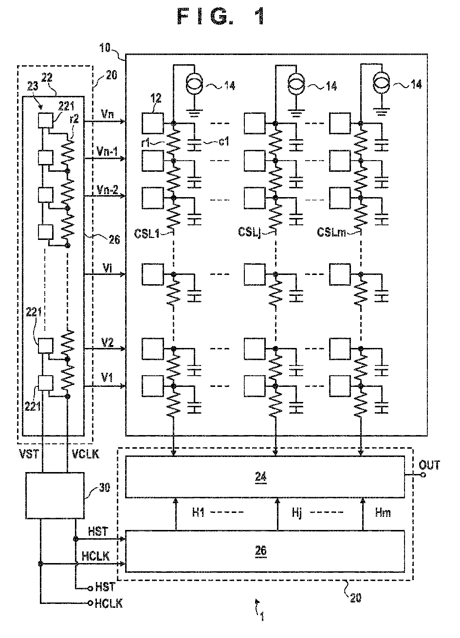
- Fig. 1 shows the arrangement of an image sensor 1 according to one embodiment of the present invention.
- the image sensor 1 includes a pixel array 10 in which a plurality of pixels 12 are arranged to form a plurality of rows and a plurality of columns, a readout portion 20 which reads out signals from the pixel array 10, and a control portion 30 which controls the readout portion 20.
- the readout portion 20 can include a row selecting portion 22, an output portion 24, and a column selecting portion 26.
- the row selecting portion 22 selects a row in the pixel array 10.
- the column selecting portion 26 selects a column in the pixel array 10.
- the output portion 24 outputs a signal from the pixel 12, of the pixels 12 on the row selected by the row selecting portion 22, which corresponds to the column selected by the column selecting portion 26.
- All the elements constituting the image sensor 1 may be arranged on one substrate or all or some of elements, other than the pixel array 10, of a plurality of pixels forming the image sensor 1 may be arranged on a substrate different from the substrate on which the pixel array 10 is arranged.
- Each pixel 12 of the pixel array 10 is controlled by a row control signal group Vi (assume that the pixel array 10 is formed by n rows, and i represents 1 to n) supplied from the row selecting portion 22.
- the row control signal group Vi can include a transfer control signal TX, a reset control signal RST, and a selecting signal SEL.
- Signals from the pixels 12 on the column selected by the row selecting portion 22 are output to column signal lines CSLj (assume that the pixel array 10 is formed by m rows, and j represents 1 to m).
- the column signal line CSLj has a parasitic resistance r1 and a parasitic capacitance c1.
- Current sources 14 are connected to the column signal lines CSLj.
- the row selecting portion 22 includes a vertical shift register 23 which shifts a vertical shift pulse in accordance with a vertical shift clock VCLK.
- the vertical shift register 23 can be formed by series-connecting a plurality of registers (for example, flip-flops) 221 which receive pulses from the preceding stage in synchronism with the vertical shift clocks VCLK.
- the vertical shift register 23 shifts a vertical shift pulse in accordance with the vertical shift clock VCLK in response to a vertical-shift start signal VST.
- the row selecting portion 22 selects a row corresponding to the position of a vertical shift pulse in the vertical shift register 23.
- the transfer path of the vertical shift clock VCLK has parasitic loads such as a parasitic resistance r2.
- the column selecting portion 26 includes a horizontal shift register which starts shifting a horizontal shift pulse in accordance with a horizontal shift clock HCLK in response to a horizontal-shift start signal HST, and selects a column corresponding to the position of the horizontal shift pulse.
- the column selecting portion 26 selects a column by setting a corresponding column selecting signal Hj at active level.
- the control portion 30 supplies the vertical shift clock VCLK and the vertical-shift start signal VST to the row selecting portion 22, and the horizontal shift clock HCLK and the horizontal-shift start signal HST to the column selecting portion 26.
- the image sensor 1 can include pads which respectively output the horizontal shift clock HCLK and the horizontal-shift start signal HST.
- the pixel 12 can include, for example, a photoelectric conversion portion (for example, photodiode) 121, a transfer transistor 122, a floating diffusion 124, a reset transistor 123, an amplification transistor 125, and a selecting transistor 126.
- the image sensor 1 may be formed as a radiation imaging apparatus which detects radiation.
- the pixel array 10 can include a scintillator which converts radiation into light.
- each photoelectric conversion portion 121 may be formed to directly convert radiation into charges.
- the charges generated by photoelectric conversion in the photoelectric conversion portion 121 are accumulated in the charge accumulation area of the photoelectric conversion portion 121.
- the transfer control signal TX goes to active level
- the transfer transistor 122 transfers the charges accumulated in the charge accumulation area of the photoelectric conversion portion 121 to the floating diffusion 124.
- the amplification transistor 125 forms a source follower, together with the current source 14 connected to the column signal line CSLj, and outputs a signal corresponding to the electric potential of the floating diffusion 124 to the column signal line CSLj.
- the reset control signal RST goes to active level, the reset transistor 123 resets the electric potential of the floating diffusion 124.
- the selecting transistor 126 When the selecting signal SEL goes to active level, the selecting transistor 126 connects the amplification transistor 125 to the column signal line CSLj. That the selecting signal SEL goes to active level indicates that the pixels on the row to which the selecting signal SEL is supplied are set in the selected state.
- the output portion 24 includes, for example, a horizontal signal line 228 and a plurality of switches 224 each of which outputs a signal from the pixel 12, of the pixels 12 on the row selected by the row selecting portion 22, which corresponds to the column selected by the column selecting portion 26.
- the output portion 24 may also include an amplifier 229 which amplifies the signal output to the horizontal signal line 228.
- the output portion 24 may also include a processing circuit 225 which processes the signal output to the column signal line CSLj.
- the processing circuit 225 can be, for example, a source follower circuit, sample/hold circuit, buffer circuit, or differential amplifier circuit.
- Fig. 3 shows a case in which the processing circuit 225 is a source follower circuit.
- the processing circuit 225 includes a transistor 226 and a current source 227.
- Fig. 7 shows a case in which the processing circuit 225 is a sample/hold circuit.
- the sample/hold circuit includes the capacitive element CP for sampling/holding a signal output to the column signal line CSLj and the switch SW provided between the column signal line CSLj and the capacitive element CP.
- the switch SW When the switch SW is turned on, the column signal line CSLj is connected to the capacitive element CP. A signal on the column signal line CSLj is written in the capacitive element CP.
- the switch SW makes transition from an ON state to an OFF state, the signal which has been written in the capacitive element CP until the transition is made is held.
- the output portion 24 may include a memory in addition to the processing circuit 225. If the memory is formed from a capacitive element, it is necessary to reset the electric potential of the horizontal signal line 228 after the capacitive element is connected to the horizontal signal line 228 via the switches 224 to output a signal.
- a parasitic load such as the parasitic resistance r2 exists in the transfer path of the vertical shift clock VCLK in the vertical shift register 23 forming the row selecting portion 22.
- the waveform of the vertical shift clock VCLK supplied to each of the registers 221 constituting the vertical shift register 23 is rounded in accordance with the distance from the control portion 30 as the supply source of the vertical shift clock VCLK. More specifically, the time required for one shift operation (the operation of shifting a pulse from one register 221 to the next register 221) increases in accordance with the distance. Therefore, the delay time from the transition timing of the vertical shift clock VCLK in the control portion 30 as the supply source of the vertical shift clock VCLK to the timing of the selection of a row increases in accordance with the distance.
- the time which can be used for readout operation decreases in accordance with the distance.
- the control portion 30 is placed nearer to the first-stage register 221 of the vertical shift register 23 than the last-stage register 221 of the vertical shift register 23.
- the parasitic resistance r1 and the parasitic capacitance c1 exist in the column signal line CSLj. Therefore, the time required to transfer a signal from a pixel on a selected row to the output portion 24 increases in accordance with the distance from the row to the output portion 24. Such a problem becomes more conspicuous in an image sensor with a large pixel array size of several tens of cm. Shortages of readout period corresponding to row positions can cause shading.
- the pixel array 10 is divided into a plurality of blocks differing in distance from the output portion 24, and different readout periods are assigned to the plurality of blocks. More specifically, the control portion 30 controls readout periods during which the readout portion 20 reads out signals from the respective blocks such that the readout portion 20 reads out signals in longer readout periods from blocks with an increase in distance from the output portion 24.
- the pixel array 10 is divided into three blocks, namely the first, second, and third blocks, in increasing order of distance from the output portion 24. Note that when the pixel array is divided into the largest number of blocks, each block is formed by one row. That is, each block is formed by at least one row.
- the control portion 30 includes, for example, a block identifying portion 310, a vertical control portion 320, a horizontal control portion 330, and a basic-signal generator 340.
- the basic-signal generator 340 generates the vertical-shift start signal VST, a basic clock mVCLK, and the horizontal shift clock HCLK.
- the block identifying portion 310 performs a counting operation in accordance with the vertical shift clocks VCLK in response to the vertical-shift start signal VST, and identifies a selected row in the pixel array 10 as a row belonging to a specific one of the plurality of blocks based on the count value. In this case, the count value coincides with the number of the row selected by the row selecting portion 22. If the row selected by the row selecting portion 22 belongs to the first block, the block identifying portion 310 sets a first block signal A1 at active level. Likewise, if the row selected by the row selecting portion 22 belongs to the second block, the block identifying portion 310 sets a second block signal A2 at active level. Likewise, if the row selected by the row selecting portion 22 belongs to the third block, the block identifying portion 310 sets a third block signal A3 at active level.
- the vertical control portion 320 includes a plurality of clock generators 321, 322, and 323 which generate clocks of periods corresponding to the corresponding blocks of the plurality of blocks (first, second, and third blocks) of the pixel array 10.
- the clocks generated by the respective clock generators 321, 322, and 323 are selected by switches 325 to 327 respectively controlled by the first to third block signals A1 to A3, and output as the vertical shift clocks VCLK.
- VP1 be the period of the clock generated by the clock generator 321 corresponding to the first block.
- VP2 be the period of the clock generated by the clock generator 322 corresponding to the second block.
- VP3 be the period of the clock generated by the clock generator 323 corresponding to the third block.
- the periods of the clocks respectively generated by the clock generators 321, 322, and 323 are determined to satisfy VP1 ⁇ VP2 ⁇ VP3. This increases the readout period required to read out a signal from a block with an increase in distance from the output portion 24.
- ⁇ is a positive number.
- ⁇ can be on the order of ns.
- the clock generator 321 can be formed to start generating a clock in response to, for example, the vertical-shift start signal VST generated by the basic-signal generator 340.
- the clock generators 322 and 323 can be formed to start generating clocks in response to clock generation start signals A2_st and A3_st respectively synchronized with the block identifying signals A2 and A3.
- the clock generators 321, 322, and 323 can be formed by, for example, a frequency dividing circuit which frequency-divides the basic clock VCLK generated by the basic-signal generator 340.
- the horizontal control portion 330 includes a plurality of timing signal generators 331, 332, and 333 which generate timing signals corresponding to the corresponding blocks of the plurality of blocks (first, second, and third blocks).
- the signals generated by the timing signal generators 331, 332, and 333 are selected by switches 335 to 337 respectively controlled by the first to third block signals A1 to A3, and output as the horizontal-shift start signals HST.
- t1 be the time of occurrence of a timing signal generated by the timing signal generator 331 corresponding to the first block
- t2 be the time of occurrence of a timing signal generated by the timing signal generator 332 corresponding to the second block
- t3 be the time of occurrence of a timing signal generated by the timing signal generator 333 corresponding to the third block.
- the timing signal generators 331, 332, and 333 are formed to increase the time from the selection of a row by the row selecting portion 22 to the generation of the horizontal-shift start signal HST for a corresponding block with an increase in distance from the output portion 24.
- the timing signal generators 331, 332, and 333 can be formed from, for example, a counter which counts the horizontal shift clocks HCLK generated by the basic-signal generator 340. This counter can be formed to start counting in response to the vertical shift clock VCLK generated by the vertical control portion 320.
- the timing signal generators 331, 332, and 333 can be formed from other circuit elements such as delay elements.
- Fig. 5 schematically shows an operation method for the image sensor 1.
- "One row of first block” indicates the operation of reading out a signal from one row of the first block.
- "One row of second block” indicates the operation of reading out a signal from one row of the second block.
- "One row of third block” indicates the operation of reading out a signal from one row of the third block.
- the vertical shift clock VCLK has the period VP1 when reading out a signal from a row of the first block.
- the vertical shift clock VCLK has the period VP2 when reading out a signal from a row of the second block.
- the vertical shift clock VCLK has the period VP3 when reading out a signal from a row of the third block.
- acc1 be the time from a leading edge of the vertical shift clock VCLK to the generation of the horizontal-shift start signal HST when reading out a signal from a row of the first block
- acc2 be the time from a leading edge of the vertical shift clock VCLK to the generation of the horizontal-shift start signal HST when reading out a signal from a row of the second block
- acc3 be the time from a leading edge of the vertical shift clock VCLK to the generation of the horizontal-shift start signal HST when reading out a signal from a row of the third block.
- the relation of acc1 ⁇ acc2 ⁇ acc3 is satisfied so as to read out signals from blocks in longer readout periods as the distances from the output portion 24 increase.
- acc1 represents a readout period for the first block; acc2, a readout period for the second block; and acc3, a readout period for the third block.
- the readout period is from a predetermined time such as a time corresponding to a leading edge of the vertical shift clock VCLK to the time of completion of sampling (that is, the time of transition from an ON state to an OFF state of the switch SW).
- the switch SW can be controlled to make transition from an ON state to an OFF state in synchronism with, for example, a leading edge of the horizontal-shift start signal HST.
- control portion 30 controls readout periods required by the readout portion 20 to read out signals from a plurality of blocks so as to read out signals from block in longer readout periods as the distances from the output portion 24 increase. This makes it possible to solve the problem of shortages of readout period for blocks distant from the output portion 24 and reduce shading.
- Fig. 6 shows the arrangement of an imaging system 800 according to one embodiment of the present invention.
- the imaging system 800 includes, for example, an optical portion 810, an imaging module 820, a recording/communicating portion 840, a timing controller 850, a system controller 860, and a playback/display portion 870.
- the imaging module 820 can include the image sensor 1 described above and a processing portion 830 which processes the image signal output from the image sensor 1.
- the processing portion 830 receives an image signal in accordance with the horizontal shift clock HCLK and the horizontal-shift start signal HST output from the image sensor 1 via pads.
- the optical portion 810 forms an image of an object on an imaging plane of the image sensor 1.
- the image sensor 1 operates in accordance with a timing signal from the timing controller 850, and outputs a signal corresponding to the image formed on the imaging plane.
- the signal output from the image sensor 1 is supplied to the processing portion 830.
- the processing portion 830 performs signal processing in accordance with the method determined by a program and the like.
- the signal generated by processing in the processing portion 830 is sent as image data to the recording/communicating portion 840.
- the recording/communicating portion 840 sends a signal for the formation of an image to the playback/display portion 870.
- the playback/display portion 870 plays back and displays a moving image and a still image.
- the recording/communicating portion 840 also receives a signal from the processing portion 830 and communicates with the system controller 860. In addition, the recording/communicating portion 840 records a signal for the formation of an image on a recording medium (not shown
- the system controller 860 comprehensively controls the operation of the imaging system 800, and controls the optical portion 810, the timing controller 850, the recording/communicating portion 840, and the playback/display portion 870.
- the system controller 860 can include, for example, a storage device (not shown) as a recording medium. It is possible to record, on the storage device, programs and the like required to control the operation of the imaging system 800.
- the system controller 860 supplies, for example, a signal for changing between driving modes in accordance with the operation performed by the user to a corresponding element in the imaging system 800.
- this operation includes changing a row from which readout operation is performed, a row to be reset, and the field angle accompanying electronic zooming and shifting the field angle accompanying electronic anti-vibration operation.
- the timing controller 850 controls the driving timings of the image sensor 1 and processing portion 830 under the control of the system controller 860.
- Fig. 8 shows the arrangement of a multi-chip sensor MCS according to one embodiment of the present invention.
- the multi-chip sensor MCS is formed from an array of a plurality of image sensors (chips) 1.
- the multi-chip sensor MCS can be formed from a two-dimensional array of a plurality of image sensors 1.
- the plurality of image sensors 1 are arranged to form 2 rows x 3 columns.
- the direction of the rows (the rows forming the array) of the array of the plurality of image sensors 1 coincides with the direction of the rows of the pixel array 10 of each image sensor 1.
- the direction of the columns (the columns forming the array) of the array of the plurality of image sensors 1 coincides with the direction of the columns of the pixel array 10 of each image sensor 1.
- the plurality of image sensors 1 are arranged such that the column selecting portions 26 sandwich the sensor arrays 10.
- a side, of the two sides of the first image sensor 1 along the row direction, which is located farther from the column selecting portion 26 is close to a side, of the two sides of the second image sensor 1 along the row direction, which is located farther from the column selecting portion 26. This makes it possible to reduce the number of missing pixels in the array of the plurality of image sensors 1.
- Fig. 9A shows the arrangement of a multi-chip sensor MCS as another embodiment of the present invention.
- the multi-chip sensor MCS is formed from an array of a plurality of image sensors (chips) 1.
- Fig. 9B shows an example of the arrangement of the image sensors (chips) 1 forming the multi-chip sensor MCS shown in Fig. 9A .
- Each image sensor 1 includes pixels 12 arranged so as to form a pixel array of a plurality of rows and a plurality of columns.
- the row selecting portion 22 and the column selecting portion 26 are arranged in the pixel array.
- the row selecting portion 22 is formed from a set of a plurality of constituent elements VSR.
- Each constituent element VSR is placed between the photoelectric conversion portions 121.
- the column selecting portion 26 is formed from a set of a plurality of constituent elements HSR.
- Each constituent element HSR is placed in the corresponding pixel 12.
- the length of the image sensor 1 in the column direction is larger than the length of the image sensor 1 in the row direction.
- the length of the image sensor 1 in the column direction is 15 cm
- the length of the image sensor 1 in the row direction is 2 cm.
- a longer readout period should be assigned to a row located far from the column selecting portion 26 than a row located near the column selection portion 26.
- An image sensor has a pixel array, a readout portion configured to read out a signal from the pixel array, and a control portion which controls the readout portion.
- the readout portion includes a row selecting portion which selects a row in the pixel array, a column selecting portion which selects a column in the pixel array, and an output portion which outputs a signal from a pixel, of pixels on a row selected by the row selecting portion, which corresponds to a column selected by the column selecting portion.
- the pixel array includes blocks differing in distance from the output portion, and the control portion controls readout periods required by the readout portion to read out signals from the blocks so as to read out signals from blocks in longer readout periods as distances from the output portion increase.
Landscapes
- Engineering & Computer Science (AREA)
- Multimedia (AREA)
- Signal Processing (AREA)
- Transforming Light Signals Into Electric Signals (AREA)
Abstract
Description
- The present invention relates to an image sensor, an imaging system, a sensor, and an operation method for the image sensor.
- In an image sensor, a row selecting circuit selects a row of a pixel array, and a plurality of pixels on the selected row output signals to a plurality of column signal lines. A column selecting circuit then outputs signals from the pixels on one row while sequentially selecting a plurality of column signal lines. The image sensor sequentially performs this operation for a plurality of rows while changing a row to be selected. In a conventional image sensor, a readout period for signals is constant regardless of any row selected from a plurality of rows of a pixel array.
- However, in an image sensor including a pixel array and a horizontal output circuit which sequentially selects and outputs signals output from the pixel array to a plurality of column signal lines, a shortage of readout period can occur more with an increase in distance from the horizontal output circuit. Such a problem becomes more conspicuous in an image sensor with a large pixel array size of several tens of cm. Shortages of readout period corresponding to row positions can cause shading.
- The present invention provides a technique advantageous to reduce shading due shortages of readout period corresponding to row positions.
- A first aspect of the present invention provides an image sensor specified in
claims 1 to 10. - A second aspect of the present invention provides an imaging system specified in claim 11.
- A third aspect of the present invention provides a sensor specified in
claims 12 to 14. - A fourth aspect of the present invention provides an operation method for an image sensor specified in claim 15.
- Further features of the present invention will become apparent from the following description of exemplary embodiments with reference to the attached drawings.
-
-
Fig. 1 is a circuit diagram showing the arrangement of an image sensor according to one embodiment of the present invention; -
Fig. 2 is a circuit diagram showing an example of the arrangement of a pixel; -
Fig. 3 is a circuit diagram showing an example of the arrangement of a readout portion; -
Fig. 4 is a block diagram showing an example of the arrangement of a control portion; -
Fig. 5 is a timing chart showing an example of the operation of an image sensor according to one embodiment of the present invention; and -
Fig. 6 is a block diagram showing an example of the arrangement of an imaging system according to one embodiment of the present invention. -
Fig. 7 is a circuit diagram showing another example of the arrangement of the readout portion; -
Fig. 8 is a view showing the arrangement of a multi-chip sensor according to one embodiment of the present invention; and -
Figs. 9A and 9B are views showing the arrangement of a multi-chip sensor according to another embodiment of the present invention. - An exemplary embodiment of the present invention will be described below with reference to the accompanying drawings.
-
Fig. 1 shows the arrangement of animage sensor 1 according to one embodiment of the present invention. Theimage sensor 1 includes apixel array 10 in which a plurality ofpixels 12 are arranged to form a plurality of rows and a plurality of columns, areadout portion 20 which reads out signals from thepixel array 10, and acontrol portion 30 which controls thereadout portion 20. Thereadout portion 20 can include arow selecting portion 22, anoutput portion 24, and acolumn selecting portion 26. Therow selecting portion 22 selects a row in thepixel array 10. Thecolumn selecting portion 26 selects a column in thepixel array 10. Theoutput portion 24 outputs a signal from thepixel 12, of thepixels 12 on the row selected by therow selecting portion 22, which corresponds to the column selected by thecolumn selecting portion 26. All the elements constituting theimage sensor 1 may be arranged on one substrate or all or some of elements, other than thepixel array 10, of a plurality of pixels forming theimage sensor 1 may be arranged on a substrate different from the substrate on which thepixel array 10 is arranged. - Each
pixel 12 of thepixel array 10 is controlled by a row control signal group Vi (assume that thepixel array 10 is formed by n rows, and i represents 1 to n) supplied from therow selecting portion 22. As described later, for example, the row control signal group Vi can include a transfer control signal TX, a reset control signal RST, and a selecting signal SEL. Signals from thepixels 12 on the column selected by therow selecting portion 22 are output to column signal lines CSLj (assume that thepixel array 10 is formed by m rows, and j represents 1 to m). The column signal line CSLj has a parasitic resistance r1 and a parasitic capacitance c1.Current sources 14 are connected to the column signal lines CSLj. - The
row selecting portion 22 includes avertical shift register 23 which shifts a vertical shift pulse in accordance with a vertical shift clock VCLK. Thevertical shift register 23 can be formed by series-connecting a plurality of registers (for example, flip-flops) 221 which receive pulses from the preceding stage in synchronism with the vertical shift clocks VCLK. The vertical shift register 23 shifts a vertical shift pulse in accordance with the vertical shift clock VCLK in response to a vertical-shift start signal VST. Therow selecting portion 22 selects a row corresponding to the position of a vertical shift pulse in thevertical shift register 23. The transfer path of the vertical shift clock VCLK has parasitic loads such as a parasitic resistance r2. - The
column selecting portion 26 includes a horizontal shift register which starts shifting a horizontal shift pulse in accordance with a horizontal shift clock HCLK in response to a horizontal-shift start signal HST, and selects a column corresponding to the position of the horizontal shift pulse. Thecolumn selecting portion 26 selects a column by setting a corresponding column selecting signal Hj at active level. - The
control portion 30 supplies the vertical shift clock VCLK and the vertical-shift start signal VST to therow selecting portion 22, and the horizontal shift clock HCLK and the horizontal-shift start signal HST to thecolumn selecting portion 26. Theimage sensor 1 can include pads which respectively output the horizontal shift clock HCLK and the horizontal-shift start signal HST. -
Fig. 2 exemplifies the arrangement of onepixel 12. Thepixel 12 can include, for example, a photoelectric conversion portion (for example, photodiode) 121, atransfer transistor 122, afloating diffusion 124, areset transistor 123, anamplification transistor 125, and a selectingtransistor 126. Theimage sensor 1 may be formed as a radiation imaging apparatus which detects radiation. In this case, thepixel array 10 can include a scintillator which converts radiation into light. Alternatively, eachphotoelectric conversion portion 121 may be formed to directly convert radiation into charges. - The charges generated by photoelectric conversion in the
photoelectric conversion portion 121 are accumulated in the charge accumulation area of thephotoelectric conversion portion 121. When the transfer control signal TX goes to active level, thetransfer transistor 122 transfers the charges accumulated in the charge accumulation area of thephotoelectric conversion portion 121 to thefloating diffusion 124. Theamplification transistor 125 forms a source follower, together with thecurrent source 14 connected to the column signal line CSLj, and outputs a signal corresponding to the electric potential of thefloating diffusion 124 to the column signal line CSLj. When the reset control signal RST goes to active level, thereset transistor 123 resets the electric potential of thefloating diffusion 124. When the selecting signal SEL goes to active level, the selectingtransistor 126 connects theamplification transistor 125 to the column signal line CSLj. That the selecting signal SEL goes to active level indicates that the pixels on the row to which the selecting signal SEL is supplied are set in the selected state. -
Fig. 3 exemplifies the arrangement of theoutput portion 24. Theoutput portion 24 includes, for example, ahorizontal signal line 228 and a plurality ofswitches 224 each of which outputs a signal from thepixel 12, of thepixels 12 on the row selected by therow selecting portion 22, which corresponds to the column selected by thecolumn selecting portion 26. Theoutput portion 24 may also include anamplifier 229 which amplifies the signal output to thehorizontal signal line 228. Theoutput portion 24 may also include aprocessing circuit 225 which processes the signal output to the column signal line CSLj. - The
processing circuit 225 can be, for example, a source follower circuit, sample/hold circuit, buffer circuit, or differential amplifier circuit.Fig. 3 shows a case in which theprocessing circuit 225 is a source follower circuit. In the case shown inFig. 3 , theprocessing circuit 225 includes atransistor 226 and acurrent source 227. -
Fig. 7 shows a case in which theprocessing circuit 225 is a sample/hold circuit. The sample/hold circuit includes the capacitive element CP for sampling/holding a signal output to the column signal line CSLj and the switch SW provided between the column signal line CSLj and the capacitive element CP. When the switch SW is turned on, the column signal line CSLj is connected to the capacitive element CP. A signal on the column signal line CSLj is written in the capacitive element CP. When the switch SW makes transition from an ON state to an OFF state, the signal which has been written in the capacitive element CP until the transition is made is held. - The
output portion 24 may include a memory in addition to theprocessing circuit 225. If the memory is formed from a capacitive element, it is necessary to reset the electric potential of thehorizontal signal line 228 after the capacitive element is connected to thehorizontal signal line 228 via theswitches 224 to output a signal. - As described above, a parasitic load such as the parasitic resistance r2 exists in the transfer path of the vertical shift clock VCLK in the
vertical shift register 23 forming therow selecting portion 22. For this reason, the waveform of the vertical shift clock VCLK supplied to each of theregisters 221 constituting thevertical shift register 23 is rounded in accordance with the distance from thecontrol portion 30 as the supply source of the vertical shift clock VCLK. More specifically, the time required for one shift operation (the operation of shifting a pulse from oneregister 221 to the next register 221) increases in accordance with the distance. Therefore, the delay time from the transition timing of the vertical shift clock VCLK in thecontrol portion 30 as the supply source of the vertical shift clock VCLK to the timing of the selection of a row increases in accordance with the distance. That is, the time which can be used for readout operation (that is, the readout period) decreases in accordance with the distance. Thecontrol portion 30 is placed nearer to the first-stage register 221 of thevertical shift register 23 than the last-stage register 221 of thevertical shift register 23. - The parasitic resistance r1 and the parasitic capacitance c1 exist in the column signal line CSLj. Therefore, the time required to transfer a signal from a pixel on a selected row to the
output portion 24 increases in accordance with the distance from the row to theoutput portion 24. Such a problem becomes more conspicuous in an image sensor with a large pixel array size of several tens of cm. Shortages of readout period corresponding to row positions can cause shading. - In this embodiment, therefore, the
pixel array 10 is divided into a plurality of blocks differing in distance from theoutput portion 24, and different readout periods are assigned to the plurality of blocks. More specifically, thecontrol portion 30 controls readout periods during which thereadout portion 20 reads out signals from the respective blocks such that thereadout portion 20 reads out signals in longer readout periods from blocks with an increase in distance from theoutput portion 24. The following will describe an example in which thepixel array 10 is divided into three blocks, namely the first, second, and third blocks, in increasing order of distance from theoutput portion 24. Note that when the pixel array is divided into the largest number of blocks, each block is formed by one row. That is, each block is formed by at least one row. -
Fig. 4 exemplifies the arrangement of thecontrol portion 30. Thecontrol portion 30 includes, for example, ablock identifying portion 310, avertical control portion 320, ahorizontal control portion 330, and a basic-signal generator 340. The basic-signal generator 340 generates the vertical-shift start signal VST, a basic clock mVCLK, and the horizontal shift clock HCLK. - The
block identifying portion 310 performs a counting operation in accordance with the vertical shift clocks VCLK in response to the vertical-shift start signal VST, and identifies a selected row in thepixel array 10 as a row belonging to a specific one of the plurality of blocks based on the count value. In this case, the count value coincides with the number of the row selected by therow selecting portion 22. If the row selected by therow selecting portion 22 belongs to the first block, theblock identifying portion 310 sets a first block signal A1 at active level. Likewise, if the row selected by therow selecting portion 22 belongs to the second block, theblock identifying portion 310 sets a second block signal A2 at active level. Likewise, if the row selected by therow selecting portion 22 belongs to the third block, theblock identifying portion 310 sets a third block signal A3 at active level. - The
vertical control portion 320 includes a plurality ofclock generators pixel array 10. The clocks generated by therespective clock generators switches 325 to 327 respectively controlled by the first to third block signals A1 to A3, and output as the vertical shift clocks VCLK. - In this case, let VP1 be the period of the clock generated by the
clock generator 321 corresponding to the first block. In addition, let VP2 be the period of the clock generated by theclock generator 322 corresponding to the second block. Furthermore, let VP3 be the period of the clock generated by theclock generator 323 corresponding to the third block. In this embodiment, in order to increase the row selection time required by therow selecting portion 22 for the blocks with an increase in distance from theoutput portion 24, the periods of the clocks respectively generated by theclock generators output portion 24. For example, it is possible to set VP1, VP2, and VP3 so as to satisfy VP2 = VP1 + α and VP3 = VP1 + 2α where α is a positive number. For example, α can be on the order of ns. - The
clock generator 321 can be formed to start generating a clock in response to, for example, the vertical-shift start signal VST generated by the basic-signal generator 340. On the other hand, theclock generators clock generators signal generator 340. - The
horizontal control portion 330 includes a plurality oftiming signal generators timing signal generators switches 335 to 337 respectively controlled by the first to third block signals A1 to A3, and output as the horizontal-shift start signals HST. - In this case, let t1 be the time of occurrence of a timing signal generated by the
timing signal generator 331 corresponding to the first block, t2 be the time of occurrence of a timing signal generated by thetiming signal generator 332 corresponding to the second block, and t3 be the time of occurrence of a timing signal generated by thetiming signal generator 333 corresponding to the third block. In this embodiment, thetiming signal generators row selecting portion 22 to the generation of the horizontal-shift start signal HST for a corresponding block with an increase in distance from theoutput portion 24. In other words, thetiming signal generators row selecting portion 22 selects a row to the instant theoutput portion 24 starts outputting a signal from the first pixel on the row increases for the corresponding block with an increase in distance from theoutput portion 24. More specifically, thetiming signal generators readout portion 20 read out a signal from a block in a longer readout period as the distance from theoutput portion 24 increases. For example, t1, t2, and t3 can be set to satisfy t2 = t1 + β and t3 = t1 + 2β where β is a positive number. - The
timing signal generators signal generator 340. This counter can be formed to start counting in response to the vertical shift clock VCLK generated by thevertical control portion 320. Alternatively, thetiming signal generators -
Fig. 5 schematically shows an operation method for theimage sensor 1. "One row of first block" indicates the operation of reading out a signal from one row of the first block. "One row of second block" indicates the operation of reading out a signal from one row of the second block. "One row of third block" indicates the operation of reading out a signal from one row of the third block. - The vertical shift clock VCLK has the period VP1 when reading out a signal from a row of the first block. The vertical shift clock VCLK has the period VP2 when reading out a signal from a row of the second block. The vertical shift clock VCLK has the period VP3 when reading out a signal from a row of the third block. As described above, the relation of VP1 < VP2 < VP3 is satisfied so as to read out signals from blocks in longer readout periods as the distances from the
output portion 24 increase. - Let acc1 be the time from a leading edge of the vertical shift clock VCLK to the generation of the horizontal-shift start signal HST when reading out a signal from a row of the first block, acc2 be the time from a leading edge of the vertical shift clock VCLK to the generation of the horizontal-shift start signal HST when reading out a signal from a row of the second block, and acc3 be the time from a leading edge of the vertical shift clock VCLK to the generation of the horizontal-shift start signal HST when reading out a signal from a row of the third block. The relation of acc1 < acc2 < acc3 is satisfied so as to read out signals from blocks in longer readout periods as the distances from the
output portion 24 increase. - If the
processing circuit 225 has the arrangement shown inFig. 3 , acc1 represents a readout period for the first block; acc2, a readout period for the second block; and acc3, a readout period for the third block. In contrast to this, if theprocessing circuit 225 has the arrangement shown inFig. 7 , the readout period is from a predetermined time such as a time corresponding to a leading edge of the vertical shift clock VCLK to the time of completion of sampling (that is, the time of transition from an ON state to an OFF state of the switch SW). The switch SW can be controlled to make transition from an ON state to an OFF state in synchronism with, for example, a leading edge of the horizontal-shift start signal HST. - As described above, according to this embodiment, the
control portion 30 controls readout periods required by thereadout portion 20 to read out signals from a plurality of blocks so as to read out signals from block in longer readout periods as the distances from theoutput portion 24 increase. This makes it possible to solve the problem of shortages of readout period for blocks distant from theoutput portion 24 and reduce shading. -
Fig. 6 shows the arrangement of animaging system 800 according to one embodiment of the present invention. Theimaging system 800 includes, for example, anoptical portion 810, animaging module 820, a recording/communicatingportion 840, atiming controller 850, asystem controller 860, and a playback/display portion 870. Theimaging module 820 can include theimage sensor 1 described above and aprocessing portion 830 which processes the image signal output from theimage sensor 1. Theprocessing portion 830 receives an image signal in accordance with the horizontal shift clock HCLK and the horizontal-shift start signal HST output from theimage sensor 1 via pads. - The
optical portion 810 forms an image of an object on an imaging plane of theimage sensor 1. Theimage sensor 1 operates in accordance with a timing signal from thetiming controller 850, and outputs a signal corresponding to the image formed on the imaging plane. The signal output from theimage sensor 1 is supplied to theprocessing portion 830. Theprocessing portion 830 performs signal processing in accordance with the method determined by a program and the like. The signal generated by processing in theprocessing portion 830 is sent as image data to the recording/communicatingportion 840. The recording/communicatingportion 840 sends a signal for the formation of an image to the playback/display portion 870. The playback/display portion 870 plays back and displays a moving image and a still image. The recording/communicatingportion 840 also receives a signal from theprocessing portion 830 and communicates with thesystem controller 860. In addition, the recording/communicatingportion 840 records a signal for the formation of an image on a recording medium (not shown). - The
system controller 860 comprehensively controls the operation of theimaging system 800, and controls theoptical portion 810, thetiming controller 850, the recording/communicatingportion 840, and the playback/display portion 870. In addition, thesystem controller 860 can include, for example, a storage device (not shown) as a recording medium. It is possible to record, on the storage device, programs and the like required to control the operation of theimaging system 800. In addition, thesystem controller 860 supplies, for example, a signal for changing between driving modes in accordance with the operation performed by the user to a corresponding element in theimaging system 800. More specifically, for example, this operation includes changing a row from which readout operation is performed, a row to be reset, and the field angle accompanying electronic zooming and shifting the field angle accompanying electronic anti-vibration operation. Thetiming controller 850 controls the driving timings of theimage sensor 1 andprocessing portion 830 under the control of thesystem controller 860. -
Fig. 8 shows the arrangement of a multi-chip sensor MCS according to one embodiment of the present invention. The multi-chip sensor MCS is formed from an array of a plurality of image sensors (chips) 1. For example, the multi-chip sensor MCS can be formed from a two-dimensional array of a plurality ofimage sensors 1. In the case shown inFig. 8 , the plurality ofimage sensors 1 are arranged to form 2 rows x 3 columns. In this case, the direction of the rows (the rows forming the array) of the array of the plurality ofimage sensors 1 coincides with the direction of the rows of thepixel array 10 of eachimage sensor 1. In addition, the direction of the columns (the columns forming the array) of the array of the plurality ofimage sensors 1 coincides with the direction of the columns of thepixel array 10 of eachimage sensor 1. - In the case shown in
Fig. 8 , in addition, the plurality ofimage sensors 1 are arranged such that thecolumn selecting portions 26 sandwich thesensor arrays 10. In other words, on each column of the array of the plurality ofimage sensors 1, a side, of the two sides of thefirst image sensor 1 along the row direction, which is located farther from thecolumn selecting portion 26 is close to a side, of the two sides of thesecond image sensor 1 along the row direction, which is located farther from thecolumn selecting portion 26. This makes it possible to reduce the number of missing pixels in the array of the plurality ofimage sensors 1. -
Fig. 9A shows the arrangement of a multi-chip sensor MCS as another embodiment of the present invention. The multi-chip sensor MCS is formed from an array of a plurality of image sensors (chips) 1.Fig. 9B shows an example of the arrangement of the image sensors (chips) 1 forming the multi-chip sensor MCS shown inFig. 9A . Eachimage sensor 1 includespixels 12 arranged so as to form a pixel array of a plurality of rows and a plurality of columns. In the case shown inFigs. 9A and 9B , therow selecting portion 22 and thecolumn selecting portion 26 are arranged in the pixel array. Therow selecting portion 22 is formed from a set of a plurality of constituent elements VSR. Each constituent element VSR is placed between thephotoelectric conversion portions 121. In addition, thecolumn selecting portion 26 is formed from a set of a plurality of constituent elements HSR. Each constituent element HSR is placed in the correspondingpixel 12. - In the case shown in
Figs. 8 to 9B , the length of theimage sensor 1 in the column direction is larger than the length of theimage sensor 1 in the row direction. For example, the length of theimage sensor 1 in the column direction is 15 cm, and the length of theimage sensor 1 in the row direction is 2 cm. In this arrangement in which the length of theimage sensor 1 in the column direction is larger than the length of theimage sensor 1 in the row direction, a longer readout period should be assigned to a row located far from thecolumn selecting portion 26 than a row located near thecolumn selection portion 26. - While the present invention has been described with reference to exemplary embodiments, it is to be understood that the invention is not limited to the disclosed exemplary embodiments. The scope of the following claims is to be accorded the broadest interpretation so as to encompass all such modifications and equivalent structures and functions.
- An image sensor has a pixel array, a readout portion configured to read out a signal from the pixel array, and a control portion which controls the readout portion. The readout portion includes a row selecting portion which selects a row in the pixel array, a column selecting portion which selects a column in the pixel array, and an output portion which outputs a signal from a pixel, of pixels on a row selected by the row selecting portion, which corresponds to a column selected by the column selecting portion. The pixel array includes blocks differing in distance from the output portion, and the control portion controls readout periods required by the readout portion to read out signals from the blocks so as to read out signals from blocks in longer readout periods as distances from the output portion increase.
Claims (15)
- An image sensor comprising:a pixel array in which a plurality of pixels are arranged so as to form a plurality of rows and a plurality of columns;a readout portion configured to read out a signal from the pixel array; anda control portion configured to control the readout portion,wherein the readout portion includesa row selecting portion configured to select a row in the pixel array,a column selecting portion configured to select a column in the pixel array, andan output portion configured to output a signal from a pixel, of pixels on a row selected by the row selecting portion, which corresponds to a column selected by the column selecting portion,wherein the pixel array includes a plurality of blocks differing in distance from the output portion, andwherein the control portion controls readout periods required by the readout portion to read out signals from the plurality of blocks so as to read out signals from blocks in longer readout periods as distances from the output portion increase.
- The sensor according to claim 1, wherein the output portion includes a horizontal signal line and a plurality of switches configured to output a signal from a pixel, of pixels on a row selected by the row selecting portion, which corresponds to a column selected by the column selecting portion to the horizontal signal line.
- The sensor according to claim 1 or 2, wherein the control portion controls the row selecting portion so as to increase a row selection time taken by the row selecting portion for a block with an increase in distance from the output portion.
- The sensor according to any one of claims 1 to 3, wherein the row selecting portion includes a vertical shift register configured to shift a vertical shift pulse in accordance with a vertical shift clock and selects a row corresponding to a position of the vertical shift pulse, and
the control portion increases a period of the vertical shift clock when the row selecting portion selects a row of a block with an increase in distance from the output portion. - The sensor according to claim 4, wherein a supply source for the vertical shift clock is placed nearer to a first-stage register of the vertical shift register than a last-stage register of the vertical shift register.
- The sensor according to any one of claims 1 to 5, wherein the control portion controls the column selecting portion so as to increase a length of time from the selection of a row by the row selecting portion to the beginning of an output by the output portion from a first pixel of the row for a block with an increase in distance from the output portion.
- The sensor according to any one of claims 1 to 6, wherein the column selecting portion includes a horizontal shift register configured to start shifting a horizontal shift pulse in accordance with a horizontal shift clock in response to a horizontal-shift start signal generated by the control portion and selects a column corresponding to a position of the horizontal shift pulse, and
the control portion increases a time from selection of a row by the row selecting portion to generation of the horizontal-shift start signal when the row selecting portion selects a row of a block with an increase in distance from the output portion. - The sensor according to any one of claims 1 to 3, wherein the control portion includes a vertical control portion and a horizontal control portion,
the vertical control portion includes a plurality of clock generators configured to generate clocks of periods corresponding to corresponding blocks of the plurality of blocks, and supplies a clock generated by a clock generator, of the plurality of clock generators, which corresponds to a block belonging to a row selected by the row selecting portion as a vertical shift clock to the row selecting portion,
the horizontal control portion includes a plurality of timing signal generators configured to generate signals corresponding to corresponding blocks of the plurality of blocks, and supplies a timing signal generated by a timing signal generator, of the plurality of timing signal generators, which corresponds to a block belonging to a row selected by the row selecting portion as a horizontal-shift start signal to the column selecting portion,
the row selecting portion includes a vertical shift register configured to shift a vertical shift pulse in accordance with the vertical shift clock and selects a row corresponding to a position of the vertical shift pulse, and
the column selecting portion includes a horizontal shift register configured to start shifting a horizontal shift pulse in accordance with a horizontal shift clock in response to the horizontal-shift start signal and selects a column corresponding to a position of the horizontal shift pulse. - The sensor according to claim 8, further comprising pads configured to respectively output the horizontal-shift start signal and the horizontal shift clock.
- The sensor according to any one of claims 1 to 9, wherein the output portion includes a sample/hold circuit configured to sample/hold a signal from a pixel, of pixels on a row selected by the row selecting portion, which is included in a column selected by the column selecting portion, and the readout period is a time from a predetermined time to a time of completion of sampling by the sample/hold circuit.
- An imaging system comprising:an image sensor defined in any one of claims 1 to 10; anda processing portion configured to process a signal output from the image sensor.
- A sensor comprising an array of a plurality of image sensors defined in any one of claims 1 to 10.
- The sensor according to claim 12, wherein each of the plurality of image sensors has a larger length in a column direction than in a row direction.
- The sensor according to claim 11 or 12, wherein on each column of the array of the plurality of image sensors, a side, of two sides of the first image sensor along the row direction, which is farther from the column selecting portion of the first image sensor is close to a side, of two sides of the second image sensor along the row direction, which is farther from the column selecting portion of the second image sensor.
- An operation method for an image sensor including a pixel array in which a plurality of pixels are arranged so as to form a plurality of rows and a plurality of columns and a readout portion configured to read out a signal from the pixel array,
wherein the readout portion includes a row selecting portion configured to select a row in the pixel array, a column selecting portion configured to select a column in the pixel array, and an output portion configured to output a signal from a pixel, of pixels on a row selected by the row selecting portion, which corresponds to a column selected by the column selecting portion, the pixel array includes a plurality of blocks differing in distance from the output portion, and
wherein the operation method comprises controlling readout periods required by the readout portion to read out signals from the plurality of blocks so as to read out signals from blocks in longer readout periods as distances from the output portion increase.
Applications Claiming Priority (2)
| Application Number | Priority Date | Filing Date | Title |
|---|---|---|---|
| JP2013140196 | 2013-07-03 | ||
| JP2014102732A JP2015029259A (en) | 2013-07-03 | 2014-05-16 | IMAGING DEVICE, IMAGING SYSTEM, SENSOR, AND OPERATION METHOD OF IMAGING DEVICE |
Publications (1)
| Publication Number | Publication Date |
|---|---|
| EP2822269A1 true EP2822269A1 (en) | 2015-01-07 |
Family
ID=50943143
Family Applications (1)
| Application Number | Title | Priority Date | Filing Date |
|---|---|---|---|
| EP14172276.9A Withdrawn EP2822269A1 (en) | 2013-07-03 | 2014-06-13 | Image sensor, imaging system, sensor, and operation method for image sensor |
Country Status (7)
| Country | Link |
|---|---|
| US (1) | US9154719B2 (en) |
| EP (1) | EP2822269A1 (en) |
| JP (1) | JP2015029259A (en) |
| KR (1) | KR20150004755A (en) |
| CN (1) | CN104284109A (en) |
| PH (1) | PH12014000183A1 (en) |
| RU (1) | RU2014127122A (en) |
Families Citing this family (6)
| Publication number | Priority date | Publication date | Assignee | Title |
|---|---|---|---|---|
| JP6362328B2 (en) | 2013-12-26 | 2018-07-25 | キヤノン株式会社 | Solid-state imaging device and driving method thereof |
| JP6274904B2 (en) | 2014-02-25 | 2018-02-07 | キヤノン株式会社 | Solid-state imaging device and imaging system |
| CN107534049B (en) * | 2015-04-24 | 2021-07-20 | 索尼公司 | Solid-state image elements, semiconductor devices, and electronic equipment |
| US9999039B2 (en) * | 2015-07-23 | 2018-06-12 | Qualcomm Incorporated | Semi-persistent scheduling for enhanced machine type communications |
| US11012653B2 (en) * | 2019-10-14 | 2021-05-18 | Pixart Imaging Inc. | Image sensor apparatus and method capable of rapidly reading out and processing pixel voltages of pixel array |
| TWI820687B (en) * | 2022-04-26 | 2023-11-01 | 友達光電股份有限公司 | Image sensor and driving method thereof |
Citations (4)
| Publication number | Priority date | Publication date | Assignee | Title |
|---|---|---|---|---|
| EP1850582A1 (en) * | 2006-04-27 | 2007-10-31 | Canon Kabushiki Kaisha | Imaging apparatus, radiation imaging apparatus, and radiation imaging system |
| EP1903776A2 (en) * | 2006-08-31 | 2008-03-26 | Canon Kabushiki Kaisha | Imaging apparatus, method for driving the same and radiation imaging system |
| US20080291304A1 (en) * | 2007-03-06 | 2008-11-27 | Canon Kabushiki Kaisha | Imaging device and driving method thereof |
| EP2059020A2 (en) * | 2007-10-24 | 2009-05-13 | Canon Kabushiki Kaisha | Image sensor, imaging system, and image sensor driving method |
Family Cites Families (5)
| Publication number | Priority date | Publication date | Assignee | Title |
|---|---|---|---|---|
| US20050007460A1 (en) * | 2003-07-08 | 2005-01-13 | Stavely Donald J. | Systems and methods for counteracting lens vignetting |
| JP4974596B2 (en) * | 2005-07-22 | 2012-07-11 | キヤノン株式会社 | Imaging apparatus and control method thereof |
| US7593050B2 (en) | 2006-02-27 | 2009-09-22 | Eastman Kodak Company | Delay management circuit for reading out large S/H arrays |
| JP2010062965A (en) * | 2008-09-05 | 2010-03-18 | Sony Corp | Solid imaging device and camera |
| JP5010655B2 (en) * | 2009-09-07 | 2012-08-29 | 株式会社東芝 | Solid-state imaging device |
-
2014
- 2014-05-16 JP JP2014102732A patent/JP2015029259A/en active Pending
- 2014-06-13 EP EP14172276.9A patent/EP2822269A1/en not_active Withdrawn
- 2014-06-25 US US14/314,141 patent/US9154719B2/en not_active Expired - Fee Related
- 2014-06-27 PH PH12014000183A patent/PH12014000183A1/en unknown
- 2014-06-30 CN CN201410305535.XA patent/CN104284109A/en not_active Withdrawn
- 2014-07-02 RU RU2014127122A patent/RU2014127122A/en not_active Application Discontinuation
- 2014-07-02 KR KR1020140082321A patent/KR20150004755A/en not_active Abandoned
Patent Citations (4)
| Publication number | Priority date | Publication date | Assignee | Title |
|---|---|---|---|---|
| EP1850582A1 (en) * | 2006-04-27 | 2007-10-31 | Canon Kabushiki Kaisha | Imaging apparatus, radiation imaging apparatus, and radiation imaging system |
| EP1903776A2 (en) * | 2006-08-31 | 2008-03-26 | Canon Kabushiki Kaisha | Imaging apparatus, method for driving the same and radiation imaging system |
| US20080291304A1 (en) * | 2007-03-06 | 2008-11-27 | Canon Kabushiki Kaisha | Imaging device and driving method thereof |
| EP2059020A2 (en) * | 2007-10-24 | 2009-05-13 | Canon Kabushiki Kaisha | Image sensor, imaging system, and image sensor driving method |
Also Published As
| Publication number | Publication date |
|---|---|
| US20150009371A1 (en) | 2015-01-08 |
| RU2014127122A (en) | 2016-01-27 |
| JP2015029259A (en) | 2015-02-12 |
| US9154719B2 (en) | 2015-10-06 |
| CN104284109A (en) | 2015-01-14 |
| KR20150004755A (en) | 2015-01-13 |
| PH12014000183A1 (en) | 2016-01-11 |
Similar Documents
| Publication | Publication Date | Title |
|---|---|---|
| US9154719B2 (en) | Image sensor, imaging system, sensor, and operation method for image sensor | |
| KR101143641B1 (en) | Solid?state imaging device, and control method and device for driving unit component of solid?state imaging device | |
| JP5885401B2 (en) | Solid-state imaging device and imaging system | |
| US8159573B2 (en) | Photoelectric conversion device and imaging system | |
| JP5311954B2 (en) | Driving method of solid-state imaging device | |
| US7787037B2 (en) | Imaging method that continuously outputs a signal based on electric charges generated by a selected pixel unit without performing an operation of deselecting the selected pixel unit | |
| CN101841664B (en) | Solid-state image capture device, its driving method and electronic device | |
| KR101188598B1 (en) | Image processing method, semiconductor device for detecting physical quantity distribution, and electronic apparatus | |
| CN103856728A (en) | Solid-state imaging device, and electronic system | |
| CN103248840A (en) | Imaging apparatus, x-ray detector, and imaging method | |
| JP2015056876A (en) | Solid-state imaging device, method for driving the same, and imaging system | |
| US8553121B2 (en) | Imaging apparatus and control method thereof | |
| JP5400428B2 (en) | Imaging device, imaging device, and driving method thereof | |
| JP5822547B2 (en) | Imaging apparatus and imaging system | |
| JP2006093816A (en) | Solid-state imaging device | |
| US7474346B2 (en) | Image processing device and method for reading image signal from a matrix type solid state image-pickup element | |
| US7324146B2 (en) | Image processing device, image processing method and solid-state image-pickup device | |
| CN116686300A (en) | Flat-panel detector and method for performing flat-panel detector | |
| US7080785B2 (en) | Image-processing device, image-processing method and solid-state image-pickup device | |
| JP2008283457A (en) | Data transfer circuit, solid-state imaging device, and camera system | |
| JP5627373B2 (en) | Imaging apparatus, control method thereof, and program | |
| US7379108B2 (en) | Image sensor, driving method and camera | |
| JP6192790B2 (en) | Imaging apparatus and imaging system | |
| US20040195599A1 (en) | Image-processing device, image-processing method and solid-state image pickup device | |
| JP6022012B2 (en) | Imaging apparatus and imaging system |
Legal Events
| Date | Code | Title | Description |
|---|---|---|---|
| PUAI | Public reference made under article 153(3) epc to a published international application that has entered the european phase |
Free format text: ORIGINAL CODE: 0009012 |
|
| 17P | Request for examination filed |
Effective date: 20140613 |
|
| AK | Designated contracting states |
Kind code of ref document: A1 Designated state(s): AL AT BE BG CH CY CZ DE DK EE ES FI FR GB GR HR HU IE IS IT LI LT LU LV MC MK MT NL NO PL PT RO RS SE SI SK SM TR |
|
| AX | Request for extension of the european patent |
Extension state: BA ME |
|
| R17P | Request for examination filed (corrected) |
Effective date: 20150707 |
|
| RBV | Designated contracting states (corrected) |
Designated state(s): AL AT BE BG CH CY CZ DE DK EE ES FI FR GB GR HR HU IE IS IT LI LT LU LV MC MK MT NL NO PL PT RO RS SE SI SK SM TR |
|
| GRAP | Despatch of communication of intention to grant a patent |
Free format text: ORIGINAL CODE: EPIDOSNIGR1 |
|
| INTG | Intention to grant announced |
Effective date: 20160523 |
|
| STAA | Information on the status of an ep patent application or granted ep patent |
Free format text: STATUS: THE APPLICATION HAS BEEN WITHDRAWN |
|
| 18W | Application withdrawn |
Effective date: 20160920 |