JP6022012B2 - Imaging apparatus and imaging system - Google Patents
Imaging apparatus and imaging system Download PDFInfo
- Publication number
- JP6022012B2 JP6022012B2 JP2015198830A JP2015198830A JP6022012B2 JP 6022012 B2 JP6022012 B2 JP 6022012B2 JP 2015198830 A JP2015198830 A JP 2015198830A JP 2015198830 A JP2015198830 A JP 2015198830A JP 6022012 B2 JP6022012 B2 JP 6022012B2
- Authority
- JP
- Japan
- Prior art keywords
- drive signal
- unit
- transmission unit
- signal processing
- signal transmission
- Prior art date
- Legal status (The legal status is an assumption and is not a legal conclusion. Google has not performed a legal analysis and makes no representation as to the accuracy of the status listed.)
- Active
Links
Images


Landscapes
- Transforming Light Signals Into Electric Signals (AREA)
Description
本発明は撮像装置に関し、特に、画素アレイの列に対応して信号処理回路を備える撮像装置に関する。 The present invention relates to an imaging apparatus, and more particularly to an imaging apparatus including a signal processing circuit corresponding to a column of a pixel array.
画素が行列状に配列された画素アレイの各列、あるいは複数列につき信号処理回路を設けて、並列に信号処理を行う撮像装置が一般に知られている。信号処理回路は、画素から出力された信号に対して相関二重サンプリング(Correlated Double Sampling;CDS)やオフセット調整、増幅、アナログ/デジタル変換(A/D変換)といった処理を行う。 An imaging apparatus that performs signal processing in parallel by providing a signal processing circuit for each column or a plurality of columns of a pixel array in which pixels are arranged in a matrix is generally known. The signal processing circuit performs processes such as correlated double sampling (CDS), offset adjustment, amplification, and analog / digital conversion (A / D conversion) on the signal output from the pixel.
複数の信号処理回路を駆動する駆動信号を供給する手法の例として、特許文献1に記載された技術がある。特許文献1では、複数の信号処理回路を1つのグループとした各グループ内で、駆動信号を伝達するバッファ素子を直列に接続することにより、ピーク電流の低減およびバッファ素子の数の低減を図っている。
As an example of a method for supplying a drive signal for driving a plurality of signal processing circuits, there is a technique described in
しかしながら、特許文献1に記載された構成では、各信号処理回路に対してバッファ素子を設けているため、信号処理回路の数に比例してバッファ素子の数が増大する。さらに、半導体基板に形成するに際してチップ面積が増大する。
However, since the buffer element is provided for each signal processing circuit in the configuration described in
また、信号処理回路の各グループ内で駆動信号が遅延して供給されるので、動作タイミングのマージンを長く設定する必要が生じる。つまり、動作の高速化が図りにくい。 In addition, since the drive signal is supplied with delay within each group of the signal processing circuit, it is necessary to set a long margin for the operation timing. That is, it is difficult to increase the operation speed.
本発明はバッファ素子数の増大を抑制しつつ、動作の高速化を実現する撮像装置を提供することを目的とする。 An object of the present invention is to provide an imaging apparatus that realizes a high-speed operation while suppressing an increase in the number of buffer elements.
上記課題を解決する本発明は、複数行および複数列に画素が配された画素アレイと、
前記画素アレイの前記複数列の各々に対応して各々が設けられた複数の信号処理部を、各々が有する第1の信号処理部群および第2の信号処理部群と、駆動信号を生成する駆動信号生成部と、前記駆動信号を前記駆動信号生成部から伝送する複数のバッファ回路を有する駆動信号伝送部とを有し、複数のバッファ回路は、各々の入力端子に入力された信号を反転せずに各々の出力端子から出力する、複数の第1のバッファ回路および複数の第2のバッファ回路を有し、前記複数の第2のバッファ回路のうちの1つの第2のバッファ回路の出力端子が、前記第1の信号処理部群の前記複数の信号処理部に並列に接続され、前記複数の第2のバッファ回路のうちの別の1つの第2のバッファ回路の出力端子が、前記第2の信号処理部群の前記複数の信号処理部に並列に接続され、前記複数の第1のバッファ回路のうちの1つの第1のバッファ回路の出力端子が、前記1つの第2のバッファ回路の入力端子と、前記複数の第1のバッファ回路のうちの別の1つの第1のバッファ回路の入力端子とに接続され、前記別の1つの第1のバッファ回路の出力端子が、前記別の1つの第2のバッファ回路の入力端子に接続され、前記駆動信号伝送部において、前記駆動信号生成部から前記第2の信号処理部群に前記駆動信号を伝送する全てのバッファ回路の段数が、前記駆動信号伝送部において、前記駆動信号生成部から前記第1の信号処理部群に前記駆動信号を伝送する全てのバッファ回路の段数よりも多いことを特徴とする撮像装置である。
The present invention for solving the above problems includes a pixel array in which pixels are arranged in a plurality of rows and a plurality of columns,
A first signal processing unit group and a second signal processing unit group each having a plurality of signal processing units provided corresponding to each of the plurality of columns of the pixel array, and generating a drive signal A drive signal generation unit; and a drive signal transmission unit having a plurality of buffer circuits for transmitting the drive signal from the drive signal generation unit, wherein the plurality of buffer circuits invert signals input to the respective input terminals Output from each output terminal, and a plurality of first buffer circuits and a plurality of second buffer circuits, and an output of one second buffer circuit of the plurality of second buffer circuits The terminal is connected in parallel to the plurality of signal processing units of the first signal processing unit group, and the output terminal of another one of the plurality of second buffer circuits is the The plurality of second signal processing unit groups An output terminal of one first buffer circuit of the plurality of first buffer circuits is connected in parallel to the signal processing unit, and an input terminal of the one second buffer circuit and the plurality of first buffers To the input terminal of another first buffer circuit, and the output terminal of the other first buffer circuit is connected to the input of the other second buffer circuit. The number of stages of all the buffer circuits connected to the terminal and transmitting the drive signal from the drive signal generation unit to the second signal processing unit group in the drive signal transmission unit is the drive signal transmission unit. The image pickup apparatus is characterized in that the number is larger than the number of stages of all the buffer circuits that transmit the drive signal from the signal generation unit to the first signal processing unit group .
本発明によれば、バッファ素子数の増大を抑制しつつ、動作の高速化が可能となる。 According to the present invention, it is possible to increase the operation speed while suppressing an increase in the number of buffer elements.
(第1の実施形態)
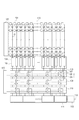
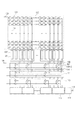
図1は、本発明の第1の実施形態に係る撮像装置の構成例を示す図である。ここではM行N列の画素101が配列された画素アレイ100と、画素アレイ100の各列に信号処理回路102を備える構成を例にとって説明する。
(First embodiment)
FIG. 1 is a diagram illustrating a configuration example of an imaging apparatus according to the first embodiment of the present invention. Here, a
画素101は光電変換部を含み、光電変換によって得られた電荷量に応じた信号を信号線VLに出力する。行選択回路103は画素101の動作を行単位で制御するもので、画素101のリセットや信号を読み出す動作を制御する。信号処理部群である信号処理回路群104の各々は複数の信号処理回路102を含み、信号線VLを介して伝達された信号を処理する回路である。信号処理回路102が備える機能の例としては、CDSによるノイズ低減、信号の増幅、A/D変換がある。A/D変換機能を有する構成では、A/D変換によって得られたデジタル信号を一時的に保持するためにSRAM(Static Random Access Memory)などのデジタルメモリを備えても良い。
The
信号処理回路102は駆動信号の供給を受けて動作する。駆動信号生成部105で生成された駆動信号は、駆動信号伝送部106、109を介して各信号処理回路102に伝達される。ここでは、信号処理部である信号処理回路102がA/D変換器とデジタルメモリを含み、それぞれを異なる駆動信号で駆動する例を示している。図示の通り、同一の信号処理回路群104に含まれる複数の信号処理回路102は共通の駆動信号が与えられるように構成される。
The
信号処理回路102から出力された信号は、転送部111を介して出力部112へと伝達され、出力端子113から後段の回路に伝達される。転送部111は、画素アレイ100の列に対応したシフトレジスタやデコーダを含み、出力部112へ信号を伝送する信号処理回路102を選択する機能を有する。転送部111は、駆動信号伝送部110を介して供給される、駆動信号生成部105で生成された駆動信号を受けて動作する。
The signal output from the
次に、駆動信号伝送部106、109、110について詳細な説明を行う。駆動信号伝送部106は、複数のバッファブロック107を有する。各バッファブロック106は、各信号処理回路群104に対して1個設けられている。各バッファブロック106は、第1のバッファ回路108−1と第2のバッファ回路108−2とを含んでなる。第1のバッファ回路の出力は他のバッファブロック107に含まれる第1及び第2のバッファ回路の入力に与えられるように接続される。また、第2バッファ回路108−2の出力は対応する信号処理回路群104の複数の信号処理回路に並列に与えられる。言い換えると、駆動信号伝送部106は、複数の第1のバッファ回路108−1が直列に接続され、第2のバッファ回路108−2は第1のバッファ回路108−1に対して並列に設けられた構成である。また、第1のバッファ回路108−1は別の第1のバッファ回路108−1及び第2のバッファ回路108−2に駆動信号を供給するとも表現できる。
Next, the drive
駆動信号伝送部109も駆動信号伝送部106と同様に、第1及び第2のバッファ回路が設けられており、各第2のバッファ回路は、複数の信号処理回路102に対して駆動信号を供給する。
Similarly to the drive
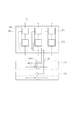
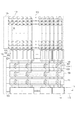
図2は、ある信号処理回路群104と、これに対応付けられた駆動信号伝送部106および109のバッファブロックの接続関係を示したブロック図である。ここでは、信号処理回路群104に3個の信号処理回路102が含まれる場合を例示した。各信号処理回路102はA/D変換器201とデジタルメモリ202とを含む。駆動信号伝送部109の第2のバッファ回路は、3個のデジタルメモリ202に駆動信号を供給し、駆動信号伝送部106の第2のバッファ回路は、3個のA/D変換器201に駆動信号を供給する。
FIG. 2 is a block diagram showing a connection relationship between a certain signal
第3の駆動信号伝送部である駆動信号伝送部110は駆動信号伝送部106と同様に、第1及び第2のバッファ回路が設けられているが、第2のバッファ回路は転送ブロックに対して駆動信号を供給する。転送ブロックの各々は例えば複数段のシフトレジスタを含み、それらに共通の駆動信号を供給する。
Similarly to the drive
本実施例の構成によれば、第2のバッファ回路から複数の信号処理回路や転送ブロックに駆動信号を供給するので、動作タイミングのマージンを短縮できるとともに、バッファ回路の数が増大することを抑制できる。また、同一の第2のバッファ回路から駆動信号を供給される信号処理回路あるいは転送ブロックは同時に動作するが、異なる第2のバッファ回路から駆動信号を供給される信号処理回路間では動作するタイミングが異なるので、ピーク電流を抑制することができる。 According to the configuration of this embodiment, the drive signal is supplied from the second buffer circuit to a plurality of signal processing circuits and transfer blocks, so that the margin of the operation timing can be shortened and the increase in the number of buffer circuits is suppressed. it can. In addition, signal processing circuits or transfer blocks to which drive signals are supplied from the same second buffer circuit operate at the same time, but there are timings between the signal processing circuits to which drive signals are supplied from different second buffer circuits. Since they are different, the peak current can be suppressed.
複数の信号処理回路102に対して共通の第2のバッファ回路から駆動信号を供給することは、信号処理回路102がA/D変換器とデジタルメモリとを含む場合に特に有用である。これは、A/D変換器は比較器とデジタルメモリとが同期して動作しなければならないため、駆動信号の位相関係を維持する必要があるからである。本実施例に示すように、駆動信号伝送部106および109のバッファブロックは、同じ信号処理回路群104に駆動信号を供給するので、信号処理回路群104の中では駆動信号の位相関係が保たれる。つまり、信号の位相管理が容易になるという利点がある。なお、本実施例では、第1の駆動信号伝送部である駆動信号伝送部106と、第2の駆動信号伝送部である駆動信号伝送部109とは、同数の第1のバッファ回路を含んで構成される例を示しているので、両者で生じる遅延時間は等しくすることができる。ここで、遅延時間が等しいとは、伝送される駆動信号がF[Hz]である場合には、2つの駆動信号伝送部が伝送する信号の間で、位相差が1周期以内であることを意味する。
Supplying a drive signal from a common second buffer circuit to the plurality of
次に、信号処理回路102がA/D変換器を含む場合の信号処理回路群104の数Sについて説明する。A/D変換器の構成として、変換対象となるアナログ信号と、時間に対してスロープ状に変化する参照信号とを比較器に入力し、参照信号が変化を開始してからアナログ信号と参照信号との大小関係が逆転するまでにカウンタに入力されるクロック数をカウントするものが知られている。このような構成のA/D変換器が複数設けられているときに、各A/D変換器に与えられるクロック信号が1周期以上遅延すると、同じレベルのアナログ信号に対してことなるデジタル信号が生成されてしまう。撮像装置においては、行に沿った方向にシェーディングとして画像に現れる。
Next, the number S of signal
図3は、駆動信号伝送部と、A〜Dで示した各ノードにおける信号の波形を示した図である。例えば、駆動信号伝送部で伝送する信号がA/D変換器におけるカウント動作を制御するためのクロック信号であるとする。クロック信号の周波数をF[Hz]として、全信号処理回路102の間で1周期、すなわち1/F[sec]以上の位相差が生じると、A/D変換結果が信号処理回路どうしで異なってしまう。このような制約の下、第1のバッファ回路で生じる遅延時間をt1[sec]、第2のバッファ回路で生じる遅延時間をt2[sec]とし、信号処理回路102がN個存在する場合を考える。
FIG. 3 is a diagram illustrating a drive signal transmission unit and signal waveforms at each node indicated by AD. For example, it is assumed that the signal transmitted by the drive signal transmission unit is a clock signal for controlling the counting operation in the A / D converter. When the frequency of the clock signal is F [Hz] and a phase difference of 1 cycle or more, that is, 1 / F [sec] or more occurs between all the
ノードAが、駆動信号生成部105から出力された駆動信号が与えられるとする。第1のバッファ回路を1段経たノードをB、さらにノードBから第2のバッファ回路を経たノードをCとし、最終段の第2のバッファ回路を経たノードをDとすると、上述の制約から、ノードAとノードDとの間で1/F[sec]よりも少ない遅延時間でなければならない。これを数式で表現すると、式(1)のように表せる。
(N/S−1)×t1+t2 < 1/F ・・・(1)
Assume that the node A is supplied with the drive signal output from the drive
(N / S-1) × t1 + t2 <1 / F (1)
したがって、信号処理回路群104の数Sを、式(1)を満たすような自然数であるように設計することで、シェーディングが生じることを抑制することができる。なお、ここではA/D変換器を例に取っているためにクロック信号として示したが、A/D変換器以外においても上記条件を満足することが好ましい。
Therefore, by designing the number S of the signal
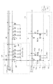
図4は、画素101の構成例を示す等価回路図である。画素101は光電変換部PD、転送トランジスタTX、リセットトランジスタRES、増幅トランジスタSF、選択トランジスタSELと、を有する。転送スイッチTXは、転送パルスPTXによって駆動され、導通すると光電変換部PDで生成された電荷が増幅トランジスタSFの制御電極のノードFDに転送される。リセットスイッチRESは、リセットパルスPRESによって駆動され、導通するとノードFDが電源電圧VDDにリセットされる。行選択スイッチSELは、行選択パルスPSELによって駆動され、導通すると増幅トランジスタは不図示の定電流源とソースフォロワ回路を構成して、ノードFDの電位に応じた信号を信号線VLに出力する。
FIG. 4 is an equivalent circuit diagram illustrating a configuration example of the
図5は、信号処理回路に含まれる増幅器と、転送部の構成例を示すである。増幅器130は、差動増幅器DIFと入力容量C0、帰還容量121a〜121c、短絡スイッチ109を含む。差動増幅器DIFの反転入力端子と出力端子とを接続する帰還容量は、信号x1、x2、x4によって選択することができるようになっており、入力容量C0の容量との容量値の比によって増幅器130のゲインが決められる。また、短絡スイッチ109が導通すると差動増幅器DIFはボルテージフォロワとして動作し、このときに出力と入力容量とを使って、画素から出力される信号をクランプすることができる。これにより、画素で生じたノイズを低減することが可能となる。
FIG. 5 shows a configuration example of the amplifier and the transfer unit included in the signal processing circuit. The
転送部は、保持容量112sおよび112nと、を含む。このうち一方に増幅器130のオフセットを保持させ、他方には増幅器130で増幅された信号を保持させる。そして、例えば出力部が持つ差動増幅器で両者の差分をとることで、増幅器130のオフセットを低減することができる。また、信号処理回路がA/D変換器を含む場合には、保持容量を廃して、デジタル信号として同様の処理を行っても良い。
The transfer unit includes holding
以上で説明したとおり、本実施例によれば、バッファ素子の数が増大することを抑制しつつ、動作の高速化を図ることができる。 As described above, according to this embodiment, it is possible to increase the operation speed while suppressing an increase in the number of buffer elements.
(第2の実施形態)
図6は、本発明の第2の実施形態に係る撮像装置の構成例を示す図である。図1に示した構成との違いは、駆動信号伝送部109に換えて駆動信号伝送部401が設けられた点である。ここでは、第1の実施形態との相違点を説明する。
(Second Embodiment)
FIG. 6 is a diagram illustrating a configuration example of an imaging apparatus according to the second embodiment of the present invention. The difference from the configuration shown in FIG. 1 is that a drive
第1の実施形態では、駆動信号伝送部109の1個のバッファブロックが3列の信号処理回路102に対して設けられていたのに対して、本実施形態では、駆動信号伝送部401の1個のバッファブロックがN/2列の信号処理回路102に対して設けられる。第1の実施形態では、駆動信号伝送部109を通して伝送される駆動信号が、駆動信号伝送部106を通して伝送される高周波数の駆動信号との間で位相関係が保たれる必要があった。このため、駆動信号伝送部109は駆動信号伝送部106と同数の信号処理回路102に対して1個のバッファブロックを設けていた。
In the first embodiment, one buffer block of the drive
一方、駆動信号伝送部401を通して伝送される信号が低周波数であれば、高周波数の駆動信号を伝送する駆動信号伝送部106よりも少ない数のバッファブロックで駆動信号伝送部401を構成できる。また、異なる駆動信号伝送部で伝送される駆動信号どうしで位相を揃える必要がない場合も同様である。図7は、第1の実施形態と比較するために、駆動信号伝送部106、109、および401を通して伝送される駆動信号の波形を示した図である。駆動信号伝送部106と109とで伝送される駆動信号との間では位相関係を保たれるのに対して、駆動信号伝送部106と401とで伝送される駆動信号の間では位相関係を保たないことを示している。駆動信号伝送部401を通して伝送する駆動信号の例としては、信号処理回路102がCDS回路を含んでいる場合にはCDS回路の動作に必要な信号、ADCを含んでいる場合には比較器をリセットするための信号や、デジタルメモリをリセットしたりカウント値をラッチしたりするための信号が該当する。
On the other hand, if the signal transmitted through the drive
さらに、信号処理回路102の構成によっては、図8に示すように、一個のバッファ回路601や602によって全列の信号処理回路102に信号を供給しても良い。このような信号は、信号処理回路102が備える増幅器のゲインを設定する信号や、動作モードを指定する信号、シフトレジスタのスタートパルスなどが例として挙げられる。
Further, depending on the configuration of the
つまり、信号処理回路102に供給する全ての信号を同じ数のバッファブロックで伝送するのではなく、伝送する駆動信号の種類に応じて駆動信号伝送部が備えるバッファ回路の数を設定することで、バッファ回路が占める面積や消費電力を適正化できる。
That is, instead of transmitting all signals supplied to the
(第3の実施形態)
図9を参照しながら、本発明の第3の実施形態について説明を行う。
(Third embodiment)
The third embodiment of the present invention will be described with reference to FIG.
図9は、信号処理回路群104の構成例を示す図である。駆動信号伝送部106から供給される駆動信号に対して逓倍あるいは分周した信号との間での位相管理が必要となる場合がある。そこで、本実施形態においては周波数変換部701を設ける。
FIG. 9 is a diagram illustrating a configuration example of the signal
各駆動信号部が備えるバッファ回路間にはばらつきや寄生負荷の違いが存在するため、駆動信号が高周波数である場合には特に、駆動信号間で位相関係を保つことが困難になる。これに対して、本実施形態では周波数変換部701を用いることで、位相関係を保つことを容易にすることができる。周波数変換部には、例えばPLL回路や分周回路を用いることができる。
Since there are variations and differences in parasitic loads between the buffer circuits included in each drive signal unit, it is difficult to maintain a phase relationship between the drive signals, particularly when the drive signals have a high frequency. On the other hand, in this embodiment, it is possible to easily maintain the phase relationship by using the
以上で説明した各実施形態に示した撮像装置は、例えば半導体基板上に形成することができる。全ての要素を同一の基板に設ける必要はなく、駆動信号生成部を、画素アレイや信号処理部、駆動信号伝送部とは別の半導体基板に設ける構成も考えられる。 The imaging device described in each embodiment described above can be formed on a semiconductor substrate, for example. It is not necessary to provide all the elements on the same substrate, and a configuration in which the drive signal generation unit is provided on a semiconductor substrate different from the pixel array, the signal processing unit, and the drive signal transmission unit is also possible.
(第4の実施形態)
次に、本実施形態に係る撮像システムの概略を、図10を用いて説明する。
(Fourth embodiment)
Next, an outline of the imaging system according to the present embodiment will be described with reference to FIG.
撮像システム1000は、例えば、光学部1010、撮像装置1001、映像信号処理回路部1030、記録・通信部1040、タイミング制御回路部1050、システムコントロール回路部1060、および再生・表示部1070を含む。撮像装置1001は、先述の各実施例で説明した撮像装置が用いられる。
The
レンズなどの光学系である光学部は1010、被写体からの光を撮像装置1001の、複数の画素が2次元状に配列された画素アレイに結像させ、被写体の像を形成する。撮像装置1001は、タイミング制御回路部1050からの信号に基づくタイミングで、画素部に結像された光に応じた信号を出力する。
An
撮像装置1001から出力された信号は、映像信号処理部である映像信号処理回路部1030に入力され、映像信号処理回路部1030が、プログラムなどによって定められた方法に従って、入力された電気信号に対してAD変換などの処理を行う。映像信号処理回路部での処理によって得られた信号は画像データとして記録・通信部1040に送られる。記録・通信部1040は、画像を形成するための信号を再生・表示部1070に送り、再生・表示部1070に動画や静止画像が再生・表示させる。記録通信部は、また、映像信号処理回路部1030からの信号を受けて、システムコントロール回路部1060とも通信を行うほか、不図示の記録媒体に、画像を形成するための信号を記録する動作も行う。
A signal output from the
システムコントロール回路部1060は、撮像システムの動作を統括的に制御するものであり、光学部1010、タイミング制御回路部1050、記録・通信部1040、および再生・表示部1070の駆動を制御する。また、システムコントロール回路部1060は、例えば記録媒体である不図示の記憶装置を備え、ここに撮像システムの動作を制御するのに必要なプログラムなどが記録される。また、システムコントロール回路部1060は、例えばユーザの操作に応じて駆動モードを切り替える信号を撮像システム内で供給する。具体的な例としては、読み出す行やリセットする行の変更、電子ズームに伴う画角の変更や、電子防振に伴う画角のずらしなどである。
The system
タイミング制御回路部1050は、制御部であるシステムコントロール回路部1060による制御に基づいて撮像装置1001および映像信号処理回路部1030の駆動タイミングを制御する。
The timing
映像信号処理回路部1030は、先述の各実施例で説明した補正係数を保持し、撮像装置1001から出力された信号に対して補正処理を行う。
The video signal
100 画素アレイ
101 画素
102 信号処理回路
103 行選択回路
104 信号処理回路群
105 駆動信号生成部
106 駆動信号伝送部
107 バッファブロック
108 第2のバッファ段
109 駆動信号伝送部
110 駆動信号伝送部
401 駆動信号伝送部
601 バッファ回路
602 バッファ回路
701 周波数変換部
VL 信号線
100
Claims (13)
前記画素アレイの前記複数列の各々に対応して各々が設けられた複数の信号処理部を、各々が有する第1の信号処理部群および第2の信号処理部群と、A first signal processing unit group and a second signal processing unit group each having a plurality of signal processing units each provided corresponding to each of the plurality of columns of the pixel array;
駆動信号を生成する駆動信号生成部と、A drive signal generator for generating a drive signal;
前記駆動信号を前記駆動信号生成部から伝送する複数のバッファ回路を有する駆動信号伝送部とを有し、A drive signal transmission unit having a plurality of buffer circuits for transmitting the drive signal from the drive signal generation unit;
複数のバッファ回路は、各々の入力端子に入力された信号を反転せずに各々の出力端子から出力する、複数の第1のバッファ回路および複数の第2のバッファ回路を有し、The plurality of buffer circuits have a plurality of first buffer circuits and a plurality of second buffer circuits that output the signals input to the respective input terminals from the respective output terminals without being inverted,
前記複数の第2のバッファ回路のうちの1つの第2のバッファ回路の出力端子が、前記第1の信号処理部群の前記複数の信号処理部に並列に接続され、An output terminal of one second buffer circuit among the plurality of second buffer circuits is connected in parallel to the plurality of signal processing units of the first signal processing unit group,
前記複数の第2のバッファ回路のうちの別の1つの第2のバッファ回路の出力端子が、前記第2の信号処理部群の前記複数の信号処理部に並列に接続され、An output terminal of another one of the plurality of second buffer circuits is connected in parallel to the plurality of signal processing units of the second signal processing unit group,
前記複数の第1のバッファ回路のうちの1つの第1のバッファ回路の出力端子が、前記1つの第2のバッファ回路の入力端子と、前記複数の第1のバッファ回路のうちの別の1つの第1のバッファ回路の入力端子とに接続され、An output terminal of one first buffer circuit of the plurality of first buffer circuits is connected to an input terminal of the one second buffer circuit and another one of the plurality of first buffer circuits. Connected to the input terminals of two first buffer circuits,
前記別の1つの第1のバッファ回路の出力端子が、前記別の1つの第2のバッファ回路の入力端子に接続され、An output terminal of the another one first buffer circuit is connected to an input terminal of the another one second buffer circuit;
前記駆動信号伝送部において、前記駆動信号生成部から前記第2の信号処理部群に前記駆動信号を伝送する全てのバッファ回路の段数が、前記駆動信号伝送部において、前記駆動信号生成部から前記第1の信号処理部群に前記駆動信号を伝送する全てのバッファ回路の段数よりも多いことを特徴とする撮像装置。In the drive signal transmission unit, the number of stages of all the buffer circuits that transmit the drive signal from the drive signal generation unit to the second signal processing unit group is determined from the drive signal generation unit in the drive signal transmission unit. An imaging apparatus, wherein the number of stages is larger than the number of stages of all buffer circuits that transmit the drive signal to the first signal processing unit group.
前記S個の信号処理部群の各々が有する前記複数の信号処理部の個数の和をN、
前記第1のバッファ回路による信号の遅延時間をt1、
前記第2のバッファ回路による信号の遅延時間をt2、
前記駆動信号の周波数をFとして、
前記Sが(N/S−1)×t1+t2 < 1/Fの関係を満たすこと
を特徴とする請求項1に記載の撮像装置。 A group of S signal processing units each having a plurality of signal processing units (natural number of S>2);
The sum of the number of the plurality of signal processing units included in each of the S signal processing unit groups is N,
The delay time of the signal by the first buffer circuit is t1,
The delay time of the signal by the second buffer circuit is t2,
The frequency of the drive signal is F ,
The imaging apparatus according to claim 1, wherein the S satisfies a relationship of (N / S−1) × t1 + t2 <1 / F.
前記第1の駆動信号伝送部と前記第2の駆動信号伝送部とは、
同じ数の前記第2のバッファ回路を有することを特徴とする請求項1または2に記載の撮像装置。 The drive signal transmission unit includes a first drive signal transmission unit and a second drive signal transmission unit,
The first drive signal transmission unit and the second drive signal transmission unit are:
The imaging apparatus according to claim 1 or 2, characterized in that it has a second buffer circuit of the same number.
前記第2の駆動信号伝送部は前記第1の駆動信号伝送部よりも少ない数の前記第2のバッファ回路を有し、
前記第2の駆動信号伝送部は、前記第1の駆動信号伝送部よりも低い周波数の駆動信号を伝送すること
を特徴とする請求項1または2に記載の撮像装置。 The drive signal transmission unit includes a first drive signal transmission unit and a second drive signal transmission unit,
The second drive signal transmission unit has a smaller number of the second buffer circuits than the first drive signal transmission unit,
Said second drive signal transmitting unit, an imaging apparatus according to claim 1 or 2, characterized in that transmitting the driving signal of the first frequency lower than the drive signal transmitting unit.
前記第3の駆動信号伝送部は、前記第2の駆動信号伝送部よりも低い周波数の駆動信号を伝送すること
を特徴とする請求項4に記載の撮像装置。 A third drive signal transmission unit for supplying the drive signal to the plurality of signal processing circuits;
The imaging apparatus according to claim 4 , wherein the third drive signal transmission unit transmits a drive signal having a frequency lower than that of the second drive signal transmission unit.
前記第1の駆動信号伝送部と前記第2の駆動信号伝送部とは、遅延時間が等しいこと
を特徴とする請求項1ないし5のいずれかに記載の撮像装置。 The drive signal transmission unit includes a first drive signal transmission unit and a second drive signal transmission unit,
Wherein the first drive signal transmitting unit and the second drive signal transmitting unit, an imaging apparatus according to any one of claims 1, wherein the delay time is equal to 5.
出力部と
前記信号処理部から出力された信号を前記出力部に転送する転送部をさらに有し、
前記転送部は、シフトレジスタまたはデコーダによって前記出力部に信号を転送する前記信号処理部を選択すること
を特徴とする請求項1ないし9のいずれかに記載の撮像装置。 The imaging apparatus further includes an output unit and a transfer unit that transfers a signal output from the signal processing unit to the output unit,
The transfer unit, an imaging apparatus according a shift register or decoder to any one of claims 1 to 9, characterized in that selects the signal processing unit for transferring the signal to the output unit.
を特徴とする請求項10に記載の撮像装置。 The imaging apparatus according to claim 10 , wherein the drive signal transmission unit further supplies the drive signal to the transfer unit.
前記撮像装置から出力された信号を処理して画像データを生成する映像信号処理部と、をさらに備えたこと
を特徴とする撮像システム。 An imaging device according to any one of claims 1 to 12 ,
Imaging system characterized by further comprising a video signal processor for generating image data by processing a signal outputted from the pre SL imaging device.
Priority Applications (1)
| Application Number | Priority Date | Filing Date | Title |
|---|---|---|---|
| JP2015198830A JP6022012B2 (en) | 2015-10-06 | 2015-10-06 | Imaging apparatus and imaging system |
Applications Claiming Priority (1)
| Application Number | Priority Date | Filing Date | Title |
|---|---|---|---|
| JP2015198830A JP6022012B2 (en) | 2015-10-06 | 2015-10-06 | Imaging apparatus and imaging system |
Related Parent Applications (1)
| Application Number | Title | Priority Date | Filing Date |
|---|---|---|---|
| JP2011130266A Division JP5822547B2 (en) | 2011-06-10 | 2011-06-10 | Imaging apparatus and imaging system |
Related Child Applications (1)
| Application Number | Title | Priority Date | Filing Date |
|---|---|---|---|
| JP2016197962A Division JP6192790B2 (en) | 2016-10-06 | 2016-10-06 | Imaging apparatus and imaging system |
Publications (2)
| Publication Number | Publication Date |
|---|---|
| JP2016029817A JP2016029817A (en) | 2016-03-03 |
| JP6022012B2 true JP6022012B2 (en) | 2016-11-09 |
Family
ID=55435525
Family Applications (1)
| Application Number | Title | Priority Date | Filing Date |
|---|---|---|---|
| JP2015198830A Active JP6022012B2 (en) | 2015-10-06 | 2015-10-06 | Imaging apparatus and imaging system |
Country Status (1)
| Country | Link |
|---|---|
| JP (1) | JP6022012B2 (en) |
Family Cites Families (5)
| Publication number | Priority date | Publication date | Assignee | Title |
|---|---|---|---|---|
| JP2006303752A (en) * | 2005-04-19 | 2006-11-02 | Sony Corp | Imaging apparatus |
| JP4226577B2 (en) * | 2005-08-22 | 2009-02-18 | マイクロン テクノロジー インコーポレイテッド | Buffering technology using structured delay skew |
| JP5493934B2 (en) * | 2010-02-03 | 2014-05-14 | ソニー株式会社 | Duty correction circuit, delay locked loop circuit, column A / D converter, solid-state imaging device, and camera system |
| JP2011166197A (en) * | 2010-02-04 | 2011-08-25 | Sony Corp | Signal transmission circuit, column a/d converter, solid-state imaging element, and camera system |
| JP5619434B2 (en) * | 2010-02-26 | 2014-11-05 | パナソニック株式会社 | Solid-state imaging device and imaging device |
-
2015
- 2015-10-06 JP JP2015198830A patent/JP6022012B2/en active Active
Also Published As
| Publication number | Publication date |
|---|---|
| JP2016029817A (en) | 2016-03-03 |
Similar Documents
| Publication | Publication Date | Title |
|---|---|---|
| US10681294B2 (en) | Solid-state imaging device and camera system | |
| US9479189B2 (en) | A/D converter, solid-state imaging device and camera system | |
| US8130295B2 (en) | Analog-to-digital converter, solid-state image pickup device, and camera system | |
| JP5868065B2 (en) | Imaging device | |
| CN101873137B (en) | Da converter, solid-state imaging device, and camera system | |
| JP6341688B2 (en) | Solid-state imaging device and imaging system | |
| US9648262B2 (en) | Imaging apparatus and imaging system | |
| JP2010147684A (en) | Solid-state imaging device, and imaging system using the same | |
| US9467636B2 (en) | Photoelectric conversion device and imaging system | |
| JP5362080B2 (en) | Solid-state imaging device and imaging system | |
| JP6025348B2 (en) | Signal transmission device, photoelectric conversion device, and imaging system | |
| JP6192790B2 (en) | Imaging apparatus and imaging system | |
| US9313426B2 (en) | Photoelectric conversion device and imaging system | |
| JP6022012B2 (en) | Imaging apparatus and imaging system | |
| JP2017005393A (en) | Imaging apparatus and imaging system | |
| JP6351691B2 (en) | Photoelectric conversion device and imaging system | |
| JP2012090313A (en) | Solid-state imaging device, and imaging system using solid-state imaging device |
Legal Events
| Date | Code | Title | Description |
|---|---|---|---|
| A977 | Report on retrieval |
Free format text: JAPANESE INTERMEDIATE CODE: A971007 Effective date: 20160815 |
|
| TRDD | Decision of grant or rejection written | ||
| A01 | Written decision to grant a patent or to grant a registration (utility model) |
Free format text: JAPANESE INTERMEDIATE CODE: A01 Effective date: 20160906 |
|
| A61 | First payment of annual fees (during grant procedure) |
Free format text: JAPANESE INTERMEDIATE CODE: A61 Effective date: 20161004 |
|
| R151 | Written notification of patent or utility model registration |
Ref document number: 6022012 Country of ref document: JP Free format text: JAPANESE INTERMEDIATE CODE: R151 |