EP2819049B1 - Dispositif avec blindage de sécurité capacitive - Google Patents
Dispositif avec blindage de sécurité capacitive Download PDFInfo
- Publication number
- EP2819049B1 EP2819049B1 EP13174078.9A EP13174078A EP2819049B1 EP 2819049 B1 EP2819049 B1 EP 2819049B1 EP 13174078 A EP13174078 A EP 13174078A EP 2819049 B1 EP2819049 B1 EP 2819049B1
- Authority
- EP
- European Patent Office
- Prior art keywords
- electrodes
- chip
- physical connection
- modulation voltage
- connection pattern
- Prior art date
- Legal status (The legal status is an assumption and is not a legal conclusion. Google has not performed a legal analysis and makes no representation as to the accuracy of the status listed.)
- Active
Links
Images


Classifications
-
- G—PHYSICS
- G06—COMPUTING; CALCULATING OR COUNTING
- G06F—ELECTRIC DIGITAL DATA PROCESSING
- G06F21/00—Security arrangements for protecting computers, components thereof, programs or data against unauthorised activity
- G06F21/70—Protecting specific internal or peripheral components, in which the protection of a component leads to protection of the entire computer
- G06F21/86—Secure or tamper-resistant housings
- G06F21/87—Secure or tamper-resistant housings by means of encapsulation, e.g. for integrated circuits
-
- G—PHYSICS
- G06—COMPUTING; CALCULATING OR COUNTING
- G06F—ELECTRIC DIGITAL DATA PROCESSING
- G06F21/00—Security arrangements for protecting computers, components thereof, programs or data against unauthorised activity
- G06F21/70—Protecting specific internal or peripheral components, in which the protection of a component leads to protection of the entire computer
- G06F21/71—Protecting specific internal or peripheral components, in which the protection of a component leads to protection of the entire computer to assure secure computing or processing of information
- G06F21/77—Protecting specific internal or peripheral components, in which the protection of a component leads to protection of the entire computer to assure secure computing or processing of information in smart cards
-
- G—PHYSICS
- G09—EDUCATION; CRYPTOGRAPHY; DISPLAY; ADVERTISING; SEALS
- G09C—CIPHERING OR DECIPHERING APPARATUS FOR CRYPTOGRAPHIC OR OTHER PURPOSES INVOLVING THE NEED FOR SECRECY
- G09C1/00—Apparatus or methods whereby a given sequence of signs, e.g. an intelligible text, is transformed into an unintelligible sequence of signs by transposing the signs or groups of signs or by replacing them by others according to a predetermined system
-
- H—ELECTRICITY
- H01—ELECTRIC ELEMENTS
- H01L—SEMICONDUCTOR DEVICES NOT COVERED BY CLASS H10
- H01L23/00—Details of semiconductor or other solid state devices
- H01L23/57—Protection from inspection, reverse engineering or tampering
- H01L23/576—Protection from inspection, reverse engineering or tampering using active circuits
-
- H—ELECTRICITY
- H04—ELECTRIC COMMUNICATION TECHNIQUE
- H04L—TRANSMISSION OF DIGITAL INFORMATION, e.g. TELEGRAPHIC COMMUNICATION
- H04L9/00—Cryptographic mechanisms or cryptographic arrangements for secret or secure communications; Network security protocols
- H04L9/08—Key distribution or management, e.g. generation, sharing or updating, of cryptographic keys or passwords
- H04L9/0861—Generation of secret information including derivation or calculation of cryptographic keys or passwords
- H04L9/0866—Generation of secret information including derivation or calculation of cryptographic keys or passwords involving user or device identifiers, e.g. serial number, physical or biometrical information, DNA, hand-signature or measurable physical characteristics
-
- H—ELECTRICITY
- H04—ELECTRIC COMMUNICATION TECHNIQUE
- H04L—TRANSMISSION OF DIGITAL INFORMATION, e.g. TELEGRAPHIC COMMUNICATION
- H04L9/00—Cryptographic mechanisms or cryptographic arrangements for secret or secure communications; Network security protocols
- H04L9/32—Cryptographic mechanisms or cryptographic arrangements for secret or secure communications; Network security protocols including means for verifying the identity or authority of a user of the system or for message authentication, e.g. authorization, entity authentication, data integrity or data verification, non-repudiation, key authentication or verification of credentials
- H04L9/3271—Cryptographic mechanisms or cryptographic arrangements for secret or secure communications; Network security protocols including means for verifying the identity or authority of a user of the system or for message authentication, e.g. authorization, entity authentication, data integrity or data verification, non-repudiation, key authentication or verification of credentials using challenge-response
- H04L9/3278—Cryptographic mechanisms or cryptographic arrangements for secret or secure communications; Network security protocols including means for verifying the identity or authority of a user of the system or for message authentication, e.g. authorization, entity authentication, data integrity or data verification, non-repudiation, key authentication or verification of credentials using challenge-response using physically unclonable functions [PUF]
-
- H—ELECTRICITY
- H01—ELECTRIC ELEMENTS
- H01L—SEMICONDUCTOR DEVICES NOT COVERED BY CLASS H10
- H01L2924/00—Indexing scheme for arrangements or methods for connecting or disconnecting semiconductor or solid-state bodies as covered by H01L24/00
- H01L2924/0001—Technical content checked by a classifier
- H01L2924/0002—Not covered by any one of groups H01L24/00, H01L24/00 and H01L2224/00
Definitions
- This invention relates to devices which incorporate a capacitive security shield.
- This shield can implement a so-called physically unclonable function (“PUF”) based on the capacitance value.
- PAF physically unclonable function
- Integrated circuits (ICs) for applications such as smartcards, RFID tags, Pay-TV chips and similar devices often contain a secret security key and carry out secret functions.
- the IC needs to be secure against attacks from the outside which aim at retrieving data from them.
- ICs may be subjected to both front-side as well as back-side attacks.
- the "front-side” of a semiconductor device is defined as the side of the semiconductor device on which circuitry is provided.
- the "backside” of the semiconductor device is defined as the side opposite to the front-side.
- Front-side attacks may consist of opening of packaged chips, and recording electrical signals from the chip with external probes.
- Back-side attacks may consist of various analysis techniques such as photon emission detection, thermal infrared detection, liquid crystal detection, voltage or electric field detection, and electromagnetic detection methods.
- PUFs Physical Unclonable Functions
- a PUF is a function that is embodied in a physical structure that is easy to evaluate but hard to characterize.
- the physical structure that contains the PUF consists of at least one random component. This random component is introduced during the manufacturing process and cannot be easily controlled.
- PUFs are described for use as a hash function and for authentication purposes. Because through PUFs the key-like data is stored essentially in a material rather than in a circuit, the technology can also be used as part of a device that needs authentication, such as a tamper detection sensor.
- PUFs Physical Uplink UDFs
- PUF' s unique identifiers for smartcards (fingerprinting) and credit cards or as a 'cheap' source for key generation (common randomness) between two parties based on the very useful properties of PUFs of the uniqueness of the responses and unclonability of the PUF.
- An important aspect of a physical structure for a PUF is that its physical properties are such that an electric property, such as a capacitance or a resistance, can be derived from it which is not (easily) reproducible. This means that the respective electrical property behaves stochastically, i.e. varies within a single semiconductor device (having multiple physical structures), varies within a single batch of semiconductor devices, and varies between multiple batches.
- a semiconductor device comprising a capacitive security shield, the capacitive security shield comprising:
- This arrangement provides multiple capacitance measurements for different electrode configurations. This increases the random nature of the capacitance function and renders cloning even more difficult.
- the second set can comprise electrodes which are grounded, and/or floating, and/or applied with a modulation voltage.
- the second set of electrodes can be divided into sub-sets, with some grounded, some floating and some modulated.
- the second set of electrodes can all be the same or they can be divided into two or more of these sub-sets.
- the second set can be considered to be a counter electrode set, although there may be other conducting bodies which also contribute to the counter electrode function.
- the first set comprises electrodes which are applied with a modulation voltage for their capacitance measurement.
- a modulation voltage is applied to electrodes of the second set, the same modulation frequency and phase can be used, or the same modulation frequency and opposite phase. In general, any phase can be used. To increase randomness or entropy, reproducible random phases can be selected.
- the device can comprise a memory which stores a sequence of different configurations of the electrodes. This memory information is used to define how the capacitance measurement is to take place.
- the memory can be part of the device which is protected by the CSS.
- the electrodes can have an area of 100 ⁇ m 2 or less. Small electrodes are able to detect small changes in the electrode capacitances induced by small external active probe devices.
- the array of electrodes may have tens to thousands of electrodes.
- the electrode array is typically a regular array of electrodes, whereas the particles are randomly distributed by the manufacturing process.
- the particles can for example have a maximum linear dimension of less than 30 ⁇ m.
- the device can be used in a smart card or an RFID tag.
- the invention also provides a method of extracting data from a semiconductor device which comprises a structure for use in a physically unclonable function, wherein the structure comprises a set of randomly distributed dielectric or conducting particles formed within a dielectric layer and a set of electrodes formed in a layer over which the set of particles are formed, wherein the method comprises:
- the invention provides a semiconductor device comprising a CSS structure which uses a set of randomly distributed dielectric or conducting particles formed within a dielectric layer.
- a set of electrodes can be configured as at least two sets, wherein a first set is used to measure a capacitance characteristic, and a second set is configured as a counter electrode set.
- the electrode configuration can be altered so that multiple measurements can be obtained.
- the invention is based on a set of single-electrode fringe capacitors that are spread over the chip area (in particular over parts that need to be protected against attacks).
- Each capacitor senses its local environment by measuring the spreading capacitance between its electrode plate and all objects and materials that are within the electric field lines emerging from the electrode plate.
- Figure 1 shows a layer 10 of electrodes over which a dielectric layer 12 is formed, in which randomly dispersed particles 14 are embedded.
- the layer 10 can be the top metallization layer of an IC, and there is an independent connection to each electrode, which then routes to processing circuitry within the IC.
- Figure 1 shows schematically field lines formed, although electric field lines through the bottom layer are omitted.
- the electrodes are divided into two sets.
- the first set comprises active electrodes 16.
- the second set comprises counter electrodes, and some of these are grounded 18 and others are floating 20.
- Figure 1 shows a cross-section through the electrodes.
- the dimensions of the electrodes in the direction perpendicular to the plane of the drawing are comparable to their dimensions in the plane, so that the electrodes are for example generally round or square in plan view.
- the chip is covered by a dielectric layer in which conducting particles with irregular shapes are distributed randomly. If an attacker removes part of the dielectric layer, or removes, damages or displaces one or more conducting particles, then the capacitances of active electrodes in the proximity of the attacked location changes. This change is also sensed if the removal or displacement of material was done before the chip is powered on.
- a sub-set of the electrodes is selected (the first set of active electrodes) to measure their capacitive response.
- a capacitance typically is measured by repetitively charging and discharging the electrode's capacitance, e.g. with a logic gate as switching element, and measuring the average charge/discharge current.
- the gate's dynamic power dissipation is proportional to the sum of the electrode capacitor and the gate's parasitic capacitance.
- the remaining non-selected electrodes are connected in a particular connection pattern to from a collective distributed counter electrode, where the electric field lines emerging from the active electrodes terminate. Field lines can also terminal on other conductors in the vicinity.
- a first sub-set can be grounded, a second sub-set can be floating, a third sub-set can be connected to a modulation voltage with the same frequency and phase as that on the active electrodes, and a fourth sub-set can be connected to a modulation voltage with the same frequency but opposite phase as that on the active electrodes.
- all electrodes of the second set can be the same - e.g. all grounded or all floating.
- the division of the counter electrodes (the second set) can be more complex as desired. There may even be more than the four sub-sets identified above.
- connection patterns can be created by removing, adding or modifying sub-sets of active or counter electrodes.
- a particular configuration of active and counter electrodes is referred to as a physical connection pattern.
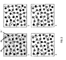
- Figure 2 shows an example of four (1 to 4) subsequent physical connection patterns of a full scan (showing a top view of part of the chip).
- the active electrodes 30 are shown with one fill pattern (these are the first set).
- the grounded counter electrodes 32 are shown with another fill pattern (these are the first sub-set of the second set) and floating counter electrodes 34 are shown with a different fill pattern (these are the second sub-set of the second set).
- the irregularly shaped forms are the conductive (or dielectric) particles.
- a full scan over the entire chip surface can be implemented by repeating a number of capacitance measurements for a set of alternative physical connection patterns.
- Figure 2 shows an example of 4 possible physical connection patterns of a full scan, i.e. 4 measurement phases.
- the number of measurement phases needed will depend on the required randomness of the measurement, on the chip area, and on the amount of parallelism in the processing of the measurements. More parallelism gives a faster scan, but requires more hardware resources on the chip.
- pairs of electrodes of a chip with 1,000 - 10,000 electrodes are compared sequentially in differential measurements, there can be 500 - 5,000 measurement phases. More realistic cases may have tens to hundreds of phases. For very accurate measurement on highly secure chips more phases can be used by reconfiguring the states of non-selected electrodes. The number of phases is also dependent on the total time available for tampering detection.
- the electrodes are made small enough then their capacitances will be less than the typical spreading capacitance of a metal probe tip that is put close enough above the dielectric layer to be able to sense electric potentials on the chip. So if someone tries to detect the electrical signal pattern produced by the active electrodes or by another circuit on the chip that is protected by the CSS by, e.g., placing a microscopic metallic tip just above the protected chip surface, then this is sensed as a change in the capacitances of the active electrodes in proximity to that tip.
- the electrode size can be a square of 1 to 5 ⁇ m side, a circle of similar diameter, or lines with similar area.
- the area is generally below 100 ⁇ m 2 so that a capacitance change which results from a small external probe can be detected.
- the particles can have largest linear dimension of 0.3 to 30 ⁇ m. The particle size and the particle density are chosen together to obtain the desired sensitivity of the capacitance function.
- the time required for a capacitance measurement depends on the noise, and on the cross-talk from other signals on the chip. It also depends on the required sensitivity of the capacitance measurement. A duration of 0.03ms - 3 ms can be required for a single capacitance measurement.
- any attempt to detect signals emerging from the chip with external probes can be detected by the chip before the attacker is able to detect the signals emerging from the chip.
- the chip can be halted or powered down, so that the attacker cannot accumulate information with long-lasting measurements.
- an attacker may be able to reveal a fixed sequence of physical connection patterns by investigating some chips (e.g. by reverse engineering), and then use that information to perform a prepared attack on another chip.
- This can be prevented by mapping a fixed sequence of logical addresses into a chip-specific sequence of physical connection patterns, e.g., with an on-chip SRAM PUF or similar.
- each chip will have its own unique sequence of physical connection patterns. In this way it is not possible to use prior information about physical connection patterns, and their relation to the logical addresses, acquired from another chip in a prepared attack.
- the SRAM PUF itself can be protected by the above CSS as well.
- the response pattern of each protected chip has to be read out in a secure terminal and stored in a database.
- Part of the database may be stored off-chip (e.g. when it is used for authentication), and part may be stored in a nonvolatile on-chip memory (when it is used for protection against attacks). This can be done by supplying a sequence of logical addresses (in case of PUFs usually called "challenges") and recording the corresponding capacitance values read from the sequence of active capacitor.
- the arrangement can use electrodes buried under a scratch protection layer or other top layer.
- a Flash or EEPROM memory can be used for the local database; with the memory protected by the CSS itself.
- Figure 3 shows a possible use of the device of the invention.
- the IC comprises the embedded memory 50, the main IC to be protected 52 and the CSS structure.
- sets of values representing the expected evaluation result of the CSS 54 are stored in the chip's internal non-volatile memory 50.
- An attempt to remove the passivation layer for example in case of reverse engineering of the chip, will irreversibly damage the CSS (i.e. the random structure of particles) and the evaluation result of the CSS will permanently deviate from the expected result.
- the chip can evaluate the CSS by the capacitance sensing and compare the evaluation result with the set of reference values in order to determine whether or not the passivation layer has been removed.
- the change can be detected by the chip autonomously in a relatively easy way.
- the CSS of the invention using randomly distributed conducting particles in the passivation layer of the chip, protects the surface of the chip in combination with a relatively easy detection scheme.
- a logical address of the embedded non volatile memory 50 is accessed. This defines the configuration pattern.
- the pattern is implemented by the integrated circuit 52 (which thus functions as the controller).
- the set of capacitance measurements are obtained from the protection CSS 54 based on a challenge and response.
- the sensed data is output is then verified based on the stored data (or else it can be verified externally).
- the electrodes are typically electrodes 5 - 25 ⁇ m apart, depending on their size and shape, and on the required sensitivity.
- all logic area and memory peripherals e.g. address decoders
- the CSS e.g. address decoders
- other circuits can be protected as well.
- the memory content typically is encrypted, and therefore doesn't necessarily need to be protected by the CSS, but it may be beneficial to protect address decoders, etc.
- the invention is of interest for encryption functions, as well as to protect a semiconductor device against tampering, i.e. attempts to obtain data stored in the semiconductor device, for example a smartcard or an RFID tag. Especially, when there is an encryption key stored in the semiconductor device a hacker may want to try to find the key in order to obtain the valid data.
- the physical structure in accordance with the invention may be advantageously applied (i.e. deposited) on top of an interconnect stack of a semiconductor device comprising an electronic circuit with secure data. Then, while trying to access the semiconductor device from the front-side the capacitance value is changed which affects the encryption key extracted . In other words, it has become very difficult to find the valid data stored in the semiconductor device.
- the invention may be applied in various application areas.
- the invention may be applied in data security for smartcards, RFID tags, Pay-TV chips, and such like.
- Such chips often contain a secret security key (encryption key) and carry out secret functions.
- the encryption key may be advantageously extracted from the physical structure in the semiconductor device in accordance with the invention.
- the invention may also be used for securing communication with, for example, a mobile phone by an internal secure key. This may then be instead of identification via the SIM card which can easily be copied.
- the protected semiconductor device can take any known form.
Claims (15)
- Dispositif semi-conducteur comprenant un blindage de sécurité capacitif, le blindage de sécurité capacitif comprenant:des particules diélectriques ou conductrices distribuées aléatoirement (14) formées à l'intérieur d'une couche diélectrique (12);caractérisé en ce que le dispositif semi-conducteur comprend en outre:une couche d'électrodes (16, 18, 20; 30, 32, 34) sur laquelle est formée la couche diélectrique (12), chaque électrode ayant une connexion indépendante; etun contrôleur (52), adapté pour configurer les électrodes dans un motif de connexion physique comportant un premier ensemble (16) d'électrodes actives utilisées pour mesurer une caractéristique de capacité, et un deuxième ensemble (18, 20) de contre-électrodes configuré comme un ensemble de non-mesure, le contrôleur étant en outre adapté pour reconfigurer des électrodes dans un motif de connexion physique différent dans lequel certaines des électrodes auparavant dans le deuxième ensemble (18, 20) sont rendues actives et certaines des électrodes auparavant dans le premier ensemble (16) sont ajoutées aux contre-électrodes.
- Dispositif selon la revendication 1, dans lequel le deuxième ensemble comprend des électrodes (18) qui sont mises à la terre.
- Dispositif selon la revendication 1 ou 2, dans lequel le deuxième ensemble comprend des électrodes (20) qui sont à un potentiel flottant.
- Dispositif selon une quelconque revendication précédente, dans lequel le deuxième ensemble comprend des électrodes qui se voient appliquer une tension de modulation.
- Dispositif selon la revendication 4, dans lequel le premier ensemble (16) comprend des électrodes qui se voient appliquer une tension de modulation, et dans lequel les électrodes du deuxième ensemble ont le même signal de modulation.
- Dispositif selon la revendication 4 ou 5, dans lequel le premier ensemble (16) comprend des électrodes qui se voient appliquer une tension de modulation, et dans lequel les électrodes du deuxième ensemble ont un signal de modulation inverse.
- Dispositif selon une quelconque revendication précédente, comprenant une mémoire (50) qui stocke une séquence de différentes configurations des électrodes.
- Dispositif selon une quelconque revendication précédente, dans lequel les électrodes (16, 18, 20; 30, 32, 34) ont une surface de 100µm2 ou moins.
- Dispositif selon une quelconque revendication précédente, dans lequel les particules (14) ont une dimension linéaire maximale de moins de 30µm.
- Carte, puce sécurisée ou étiquette RFID comprenant un dispositif selon une quelconque revendication précédente.
- Procédé d'extraction de données d'un dispositif semi-conducteur qui comprend une structure à utiliser dans une fonction physiquement inclonable, la structure comprenant des particules diélectriques ou conductrices distribuées aléatoirement (14) formées à l'intérieur d'une couche diélectrique (12) et une couche d'électrodes (16, 18, 20; 30, 32, 34) sur laquelle est formée la couche diélectrique (12),
caractérisé en ce que le procédé comprend:la configuration des électrodes sous la forme d'un motif de connexion physique comportant un premier ensemble (16) d'électrodes actives et un deuxième ensemble (18, 20) de contre-électrodes;la mesure d'une caractéristique de capacité à l'aide du premier ensemble (16), avec le deuxième ensemble (18, 20) configuré comme un ensemble de non-mesure;la reconfiguration des électrodes sous la forme d'un motif de connexion physique différent dans lequel certaines des électrodes auparavant dans le deuxième ensemble (18, 20) sont rendues actives et certaines des électrodes auparavant dans le premier ensemble (16) sont ajoutées aux contre-électrodes;la mesure d'une caractéristique de capacité reconfigurée à l'aide du premier ensemble (16) et du deuxième ensemble (18, 20) du motif de connexion physique différent. - Procédé selon la revendication 11, comprenant le réglage de la tension des électrodes du deuxième ensemble à:la terre; et/ouun potentiel flottant; et/ouune tension de modulation ou son inverse.
- Procédé selon la revendication 12, comprenant la mesure d'une caractéristique de capacité par l'application d'une tension de modulation aux électrodes du premier ensemble, et l'application aux électrodes du deuxième ensemble du même signal.
- Procédé selon la revendication 12 ou 13, comprenant la mesure d'une caractéristique de capacité par l'application d'une tension de modulation aux électrodes du premier ensemble, et l'application aux électrodes du deuxième ensemble du signal de modulation opposé.
- Procédé selon l'une quelconque des revendications 11 à 14 à utiliser dans une procédure d'authentification.
Priority Applications (3)
| Application Number | Priority Date | Filing Date | Title |
|---|---|---|---|
| EP13174078.9A EP2819049B1 (fr) | 2013-06-27 | 2013-06-27 | Dispositif avec blindage de sécurité capacitive |
| US14/293,730 US9390295B2 (en) | 2013-06-27 | 2014-06-02 | Device with capacitive security shield |
| CN201410290243.3A CN104252636B (zh) | 2013-06-27 | 2014-06-25 | 具有电容式安全屏蔽的设备 |
Applications Claiming Priority (1)
| Application Number | Priority Date | Filing Date | Title |
|---|---|---|---|
| EP13174078.9A EP2819049B1 (fr) | 2013-06-27 | 2013-06-27 | Dispositif avec blindage de sécurité capacitive |
Publications (2)
| Publication Number | Publication Date |
|---|---|
| EP2819049A1 EP2819049A1 (fr) | 2014-12-31 |
| EP2819049B1 true EP2819049B1 (fr) | 2015-11-18 |
Family
ID=48740896
Family Applications (1)
| Application Number | Title | Priority Date | Filing Date |
|---|---|---|---|
| EP13174078.9A Active EP2819049B1 (fr) | 2013-06-27 | 2013-06-27 | Dispositif avec blindage de sécurité capacitive |
Country Status (3)
| Country | Link |
|---|---|
| US (1) | US9390295B2 (fr) |
| EP (1) | EP2819049B1 (fr) |
| CN (1) | CN104252636B (fr) |
Families Citing this family (22)
| Publication number | Priority date | Publication date | Assignee | Title |
|---|---|---|---|---|
| EP3086473B1 (fr) | 2015-04-23 | 2018-03-21 | Nxp B.V. | Circuit de capteur et procédé |
| EP3147830B1 (fr) | 2015-09-23 | 2020-11-18 | Nxp B.V. | Protection d'un circuit integre |
| EP3193281B1 (fr) * | 2016-01-15 | 2019-11-13 | Nxp B.V. | Dispositif électronique |
| CN106997843B (zh) * | 2016-01-22 | 2020-05-01 | 中芯国际集成电路制造(上海)有限公司 | 半导体器件安全认证方法 |
| EP3306517A1 (fr) * | 2016-10-04 | 2018-04-11 | Nagravision S.A. | Blindage actif permettant de détecter une intrusion sur un circuit intégré |
| DK3340213T3 (da) * | 2016-12-21 | 2020-06-08 | Merck Patent Gmbh | Puf-baseret kompositsikkerhedsmærkning til bekæmpelse af vareforfalskning |
| US11388013B2 (en) * | 2017-03-31 | 2022-07-12 | Arizona Board Of Regents On Behalf Of Northern Arizona Unversity | Securing distributed elements connected to a network with addressable physically unclonable functions |
| US10622316B2 (en) | 2017-05-08 | 2020-04-14 | International Business Machines Corporation | Security arrangement for integrated circuits using microcapsules in dielectric layer |
| FR3068150B1 (fr) | 2017-06-21 | 2020-02-07 | Commissariat A L'energie Atomique Et Aux Energies Alternatives | Procede de securisation de maniere constructive d'un circuit integre lors de sa realisation |
| GB2567642B (en) * | 2017-10-17 | 2020-08-26 | Crypto Quantique Ltd | Unique identifiers based on quantum effects |
| GB201721036D0 (en) * | 2017-12-15 | 2018-01-31 | Ttp Plc | Physically unclonable function device |
| EP3550466B1 (fr) * | 2018-04-06 | 2023-08-02 | Fraunhofer-Gesellschaft zur Förderung der angewandten Forschung e.V. | Film puf et son procédé de production |
| EP3550475A1 (fr) | 2018-04-06 | 2019-10-09 | Fraunhofer-Gesellschaft zur Förderung der angewandten Forschung e.V. | Film puf et son procédé de production |
| EP3550623B1 (fr) | 2018-04-06 | 2020-07-29 | Fraunhofer-Gesellschaft zur Förderung der angewandten Forschung e.V. | Film puf et son procédé de production |
| CN109040853A (zh) * | 2018-09-04 | 2018-12-18 | 国微集团(深圳)有限公司 | 一种数字流媒体指纹水印保护方法及装置 |
| GB201908680D0 (en) | 2019-06-18 | 2019-07-31 | Ttp Plc | Temperature independent physically unclonable function device |
| GB201908679D0 (en) * | 2019-06-18 | 2019-07-31 | Ttp Plc | Environmentally dependent physically unclonable function device |
| GB2587223B (en) * | 2019-09-19 | 2023-07-19 | Pragmatic Printing Ltd | Electronic device and associated method of manufacture |
| GB201919297D0 (en) | 2019-12-24 | 2020-02-05 | Aronson Bill | Temperature sensing physical unclonable function (puf) authenication system |
| US11516028B2 (en) | 2019-12-24 | 2022-11-29 | CERA Licensing Limited | Temperature sensing physical unclonable function (PUF) authentication system |
| EP4097597A4 (fr) * | 2020-01-31 | 2023-10-11 | Hewlett-Packard Development Company, L.P. | Détermination de distributions de champ électrique |
| CN113000858B (zh) * | 2021-02-07 | 2022-05-20 | 西安交通大学 | 一种石墨烯-高熵合金复合材料及选区激光熔化制备其的方法 |
Family Cites Families (10)
| Publication number | Priority date | Publication date | Assignee | Title |
|---|---|---|---|---|
| US7663607B2 (en) * | 2004-05-06 | 2010-02-16 | Apple Inc. | Multipoint touchscreen |
| US6760357B1 (en) * | 1998-04-14 | 2004-07-06 | Bandwidth9 | Vertical cavity apparatus with tunnel junction |
| TW511398B (en) * | 2000-09-12 | 2002-11-21 | Tokyo Electron Ltd | Apparatus and method to control the uniformity of plasma by reducing radial loss |
| FI115109B (fi) * | 2003-01-22 | 2005-02-28 | Nokia Corp | Tunnistusjärjestely ja tunnistusjärjestelyn käsittävä matkaviestin |
| CN101421971A (zh) * | 2006-04-11 | 2009-04-29 | 皇家飞利浦电子股份有限公司 | 利用物理不可复制函数对令牌的询问响应认证 |
| CN101617319B (zh) * | 2007-02-20 | 2012-09-26 | Nxp股份有限公司 | 具有背面破坏防护的半导体装置 |
| US8446250B2 (en) * | 2007-06-14 | 2013-05-21 | Intrinsic Id B.V. | Method and device for providing digital security |
| JP4493686B2 (ja) * | 2007-09-27 | 2010-06-30 | 太陽誘電株式会社 | コンデンサ及びその製造方法 |
| EP2337263B1 (fr) * | 2009-12-17 | 2020-02-12 | Nxp B.V. | Jeton comportant une fonction inclonable physique améliorée |
| WO2012122994A1 (fr) * | 2011-03-11 | 2012-09-20 | Kreft Heinz | Transfert hors ligne de jetons électroniques entre dispositifs homologues |
-
2013
- 2013-06-27 EP EP13174078.9A patent/EP2819049B1/fr active Active
-
2014
- 2014-06-02 US US14/293,730 patent/US9390295B2/en active Active
- 2014-06-25 CN CN201410290243.3A patent/CN104252636B/zh active Active
Also Published As
| Publication number | Publication date |
|---|---|
| US9390295B2 (en) | 2016-07-12 |
| EP2819049A1 (fr) | 2014-12-31 |
| CN104252636B (zh) | 2017-04-12 |
| US20150007353A1 (en) | 2015-01-01 |
| CN104252636A (zh) | 2014-12-31 |
Similar Documents
| Publication | Publication Date | Title |
|---|---|---|
| EP2819049B1 (fr) | Dispositif avec blindage de sécurité capacitive | |
| Nedospasov et al. | Invasive PUF analysis | |
| Helfmeier et al. | Cloning physically unclonable functions | |
| Rahman et al. | Physical inspection & attacks: New frontier in hardware security | |
| Kömmerling et al. | Design Principles for Tamper-Resistant Smartcard Processors. | |
| US9509306B2 (en) | Tamper resistant IC | |
| US20090065591A1 (en) | Smart-card chip arrangement | |
| JP2016105278A (ja) | 耐タンパ性を有する不揮発性メモリ装置、および集積回路カード | |
| US11295003B2 (en) | Generating a unique response to a challenge | |
| CN101421971A (zh) | 利用物理不可复制函数对令牌的询问响应认证 | |
| JP2017028354A (ja) | 電子装置ネットワーク及びチップ認証方式 | |
| CN108986857A (zh) | 具有防篡改保护的集成电路及其方法 | |
| van der Leest et al. | Hardware intrinsic security to protect value in the mobile market | |
| US20200186368A1 (en) | Generating a nondeterministic response to a challenge | |
| Yang et al. | An RFID-based technology for electronic component and system counterfeit detection and traceability | |
| US20230030739A1 (en) | Physically unclonable function device | |
| Biswas et al. | On backside probing techniques and their emerging security threats | |
| Neve et al. | Memories: A survey of their secure uses in smart cards | |
| Kim et al. | Predictive analysis of 3D ReRAM-based PUF for securing the Internet of Things | |
| US11195582B2 (en) | Non-volatile memory device and method of writing to non-volatile memory device | |
| Liao et al. | The cell dependency analysis on learning sram power-up states | |
| Biswas et al. | Emerging nonvolatile memories—an assessment of vulnerability to probing attacks | |
| Biba et al. | Measurement setup for physical unclonable functions | |
| Rajan et al. | Low power physical layer security solutions for IoT devices | |
| Enamul Quadir | Physical Unclonable Functions for Authenticating and Preventing Reverse Engineering of Integrated Circuits and Electronics Hardware |
Legal Events
| Date | Code | Title | Description |
|---|---|---|---|
| PUAI | Public reference made under article 153(3) epc to a published international application that has entered the european phase |
Free format text: ORIGINAL CODE: 0009012 |
|
| 17P | Request for examination filed |
Effective date: 20131031 |
|
| AK | Designated contracting states |
Kind code of ref document: A1 Designated state(s): AL AT BE BG CH CY CZ DE DK EE ES FI FR GB GR HR HU IE IS IT LI LT LU LV MC MK MT NL NO PL PT RO RS SE SI SK SM TR |
|
| AX | Request for extension of the european patent |
Extension state: BA ME |
|
| GRAP | Despatch of communication of intention to grant a patent |
Free format text: ORIGINAL CODE: EPIDOSNIGR1 |
|
| INTG | Intention to grant announced |
Effective date: 20150316 |
|
| RBV | Designated contracting states (corrected) |
Designated state(s): AL AT BE BG CH CY CZ DE DK EE ES FI FR GB GR HR HU IE IS IT LI LT LU LV MC MK MT NL NO PL PT RO RS SE SI SK SM TR |
|
| GRAP | Despatch of communication of intention to grant a patent |
Free format text: ORIGINAL CODE: EPIDOSNIGR1 |
|
| GRAS | Grant fee paid |
Free format text: ORIGINAL CODE: EPIDOSNIGR3 |
|
| GRAA | (expected) grant |
Free format text: ORIGINAL CODE: 0009210 |
|
| INTG | Intention to grant announced |
Effective date: 20151001 |
|
| AK | Designated contracting states |
Kind code of ref document: B1 Designated state(s): AL AT BE BG CH CY CZ DE DK EE ES FI FR GB GR HR HU IE IS IT LI LT LU LV MC MK MT NL NO PL PT RO RS SE SI SK SM TR |
|
| REG | Reference to a national code |
Ref country code: GB Ref legal event code: FG4D |
|
| REG | Reference to a national code |
Ref country code: CH Ref legal event code: EP |
|
| REG | Reference to a national code |
Ref country code: AT Ref legal event code: REF Ref document number: 761876 Country of ref document: AT Kind code of ref document: T Effective date: 20151215 |
|
| REG | Reference to a national code |
Ref country code: IE Ref legal event code: FG4D |
|
| REG | Reference to a national code |
Ref country code: DE Ref legal event code: R096 Ref document number: 602013003828 Country of ref document: DE |
|
| REG | Reference to a national code |
Ref country code: NL Ref legal event code: MP Effective date: 20160218 |
|
| REG | Reference to a national code |
Ref country code: LT Ref legal event code: MG4D |
|
| REG | Reference to a national code |
Ref country code: AT Ref legal event code: MK05 Ref document number: 761876 Country of ref document: AT Kind code of ref document: T Effective date: 20151118 |
|
| PG25 | Lapsed in a contracting state [announced via postgrant information from national office to epo] |
Ref country code: HR Free format text: LAPSE BECAUSE OF FAILURE TO SUBMIT A TRANSLATION OF THE DESCRIPTION OR TO PAY THE FEE WITHIN THE PRESCRIBED TIME-LIMIT Effective date: 20151118 Ref country code: IT Free format text: LAPSE BECAUSE OF FAILURE TO SUBMIT A TRANSLATION OF THE DESCRIPTION OR TO PAY THE FEE WITHIN THE PRESCRIBED TIME-LIMIT Effective date: 20151118 Ref country code: ES Free format text: LAPSE BECAUSE OF FAILURE TO SUBMIT A TRANSLATION OF THE DESCRIPTION OR TO PAY THE FEE WITHIN THE PRESCRIBED TIME-LIMIT Effective date: 20151118 Ref country code: IS Free format text: LAPSE BECAUSE OF FAILURE TO SUBMIT A TRANSLATION OF THE DESCRIPTION OR TO PAY THE FEE WITHIN THE PRESCRIBED TIME-LIMIT Effective date: 20160318 Ref country code: NL Free format text: LAPSE BECAUSE OF FAILURE TO SUBMIT A TRANSLATION OF THE DESCRIPTION OR TO PAY THE FEE WITHIN THE PRESCRIBED TIME-LIMIT Effective date: 20151118 Ref country code: NO Free format text: LAPSE BECAUSE OF FAILURE TO SUBMIT A TRANSLATION OF THE DESCRIPTION OR TO PAY THE FEE WITHIN THE PRESCRIBED TIME-LIMIT Effective date: 20160218 Ref country code: LT Free format text: LAPSE BECAUSE OF FAILURE TO SUBMIT A TRANSLATION OF THE DESCRIPTION OR TO PAY THE FEE WITHIN THE PRESCRIBED TIME-LIMIT Effective date: 20151118 |
|
| REG | Reference to a national code |
Ref country code: FR Ref legal event code: PLFP Year of fee payment: 4 |
|
| PG25 | Lapsed in a contracting state [announced via postgrant information from national office to epo] |
Ref country code: GR Free format text: LAPSE BECAUSE OF FAILURE TO SUBMIT A TRANSLATION OF THE DESCRIPTION OR TO PAY THE FEE WITHIN THE PRESCRIBED TIME-LIMIT Effective date: 20160219 Ref country code: AT Free format text: LAPSE BECAUSE OF FAILURE TO SUBMIT A TRANSLATION OF THE DESCRIPTION OR TO PAY THE FEE WITHIN THE PRESCRIBED TIME-LIMIT Effective date: 20151118 Ref country code: PT Free format text: LAPSE BECAUSE OF FAILURE TO SUBMIT A TRANSLATION OF THE DESCRIPTION OR TO PAY THE FEE WITHIN THE PRESCRIBED TIME-LIMIT Effective date: 20160318 Ref country code: SE Free format text: LAPSE BECAUSE OF FAILURE TO SUBMIT A TRANSLATION OF THE DESCRIPTION OR TO PAY THE FEE WITHIN THE PRESCRIBED TIME-LIMIT Effective date: 20151118 Ref country code: PL Free format text: LAPSE BECAUSE OF FAILURE TO SUBMIT A TRANSLATION OF THE DESCRIPTION OR TO PAY THE FEE WITHIN THE PRESCRIBED TIME-LIMIT Effective date: 20151118 Ref country code: FI Free format text: LAPSE BECAUSE OF FAILURE TO SUBMIT A TRANSLATION OF THE DESCRIPTION OR TO PAY THE FEE WITHIN THE PRESCRIBED TIME-LIMIT Effective date: 20151118 Ref country code: RS Free format text: LAPSE BECAUSE OF FAILURE TO SUBMIT A TRANSLATION OF THE DESCRIPTION OR TO PAY THE FEE WITHIN THE PRESCRIBED TIME-LIMIT Effective date: 20151118 Ref country code: LV Free format text: LAPSE BECAUSE OF FAILURE TO SUBMIT A TRANSLATION OF THE DESCRIPTION OR TO PAY THE FEE WITHIN THE PRESCRIBED TIME-LIMIT Effective date: 20151118 |
|
| PG25 | Lapsed in a contracting state [announced via postgrant information from national office to epo] |
Ref country code: CZ Free format text: LAPSE BECAUSE OF FAILURE TO SUBMIT A TRANSLATION OF THE DESCRIPTION OR TO PAY THE FEE WITHIN THE PRESCRIBED TIME-LIMIT Effective date: 20151118 |
|
| REG | Reference to a national code |
Ref country code: DE Ref legal event code: R097 Ref document number: 602013003828 Country of ref document: DE |
|
| PG25 | Lapsed in a contracting state [announced via postgrant information from national office to epo] |
Ref country code: DK Free format text: LAPSE BECAUSE OF FAILURE TO SUBMIT A TRANSLATION OF THE DESCRIPTION OR TO PAY THE FEE WITHIN THE PRESCRIBED TIME-LIMIT Effective date: 20151118 Ref country code: SK Free format text: LAPSE BECAUSE OF FAILURE TO SUBMIT A TRANSLATION OF THE DESCRIPTION OR TO PAY THE FEE WITHIN THE PRESCRIBED TIME-LIMIT Effective date: 20151118 Ref country code: RO Free format text: LAPSE BECAUSE OF FAILURE TO SUBMIT A TRANSLATION OF THE DESCRIPTION OR TO PAY THE FEE WITHIN THE PRESCRIBED TIME-LIMIT Effective date: 20151118 Ref country code: SM Free format text: LAPSE BECAUSE OF FAILURE TO SUBMIT A TRANSLATION OF THE DESCRIPTION OR TO PAY THE FEE WITHIN THE PRESCRIBED TIME-LIMIT Effective date: 20151118 Ref country code: EE Free format text: LAPSE BECAUSE OF FAILURE TO SUBMIT A TRANSLATION OF THE DESCRIPTION OR TO PAY THE FEE WITHIN THE PRESCRIBED TIME-LIMIT Effective date: 20151118 |
|
| PLBE | No opposition filed within time limit |
Free format text: ORIGINAL CODE: 0009261 |
|
| STAA | Information on the status of an ep patent application or granted ep patent |
Free format text: STATUS: NO OPPOSITION FILED WITHIN TIME LIMIT |
|
| 26N | No opposition filed |
Effective date: 20160819 |
|
| PG25 | Lapsed in a contracting state [announced via postgrant information from national office to epo] |
Ref country code: SI Free format text: LAPSE BECAUSE OF FAILURE TO SUBMIT A TRANSLATION OF THE DESCRIPTION OR TO PAY THE FEE WITHIN THE PRESCRIBED TIME-LIMIT Effective date: 20151118 |
|
| PG25 | Lapsed in a contracting state [announced via postgrant information from national office to epo] |
Ref country code: BE Free format text: LAPSE BECAUSE OF FAILURE TO SUBMIT A TRANSLATION OF THE DESCRIPTION OR TO PAY THE FEE WITHIN THE PRESCRIBED TIME-LIMIT Effective date: 20151118 |
|
| PG25 | Lapsed in a contracting state [announced via postgrant information from national office to epo] |
Ref country code: MC Free format text: LAPSE BECAUSE OF FAILURE TO SUBMIT A TRANSLATION OF THE DESCRIPTION OR TO PAY THE FEE WITHIN THE PRESCRIBED TIME-LIMIT Effective date: 20151118 |
|
| REG | Reference to a national code |
Ref country code: CH Ref legal event code: PL |
|
| REG | Reference to a national code |
Ref country code: IE Ref legal event code: MM4A |
|
| PG25 | Lapsed in a contracting state [announced via postgrant information from national office to epo] |
Ref country code: LI Free format text: LAPSE BECAUSE OF NON-PAYMENT OF DUE FEES Effective date: 20160630 Ref country code: CH Free format text: LAPSE BECAUSE OF NON-PAYMENT OF DUE FEES Effective date: 20160630 |
|
| REG | Reference to a national code |
Ref country code: FR Ref legal event code: PLFP Year of fee payment: 5 |
|
| PG25 | Lapsed in a contracting state [announced via postgrant information from national office to epo] |
Ref country code: IE Free format text: LAPSE BECAUSE OF NON-PAYMENT OF DUE FEES Effective date: 20160627 |
|
| REG | Reference to a national code |
Ref country code: FR Ref legal event code: PLFP Year of fee payment: 6 |
|
| PG25 | Lapsed in a contracting state [announced via postgrant information from national office to epo] |
Ref country code: HU Free format text: LAPSE BECAUSE OF FAILURE TO SUBMIT A TRANSLATION OF THE DESCRIPTION OR TO PAY THE FEE WITHIN THE PRESCRIBED TIME-LIMIT; INVALID AB INITIO Effective date: 20130627 |
|
| PG25 | Lapsed in a contracting state [announced via postgrant information from national office to epo] |
Ref country code: MT Free format text: LAPSE BECAUSE OF NON-PAYMENT OF DUE FEES Effective date: 20160630 Ref country code: LU Free format text: LAPSE BECAUSE OF NON-PAYMENT OF DUE FEES Effective date: 20160627 Ref country code: MK Free format text: LAPSE BECAUSE OF FAILURE TO SUBMIT A TRANSLATION OF THE DESCRIPTION OR TO PAY THE FEE WITHIN THE PRESCRIBED TIME-LIMIT Effective date: 20151118 Ref country code: CY Free format text: LAPSE BECAUSE OF FAILURE TO SUBMIT A TRANSLATION OF THE DESCRIPTION OR TO PAY THE FEE WITHIN THE PRESCRIBED TIME-LIMIT Effective date: 20151118 |
|
| PG25 | Lapsed in a contracting state [announced via postgrant information from national office to epo] |
Ref country code: BG Free format text: LAPSE BECAUSE OF FAILURE TO SUBMIT A TRANSLATION OF THE DESCRIPTION OR TO PAY THE FEE WITHIN THE PRESCRIBED TIME-LIMIT Effective date: 20151118 |
|
| PG25 | Lapsed in a contracting state [announced via postgrant information from national office to epo] |
Ref country code: AL Free format text: LAPSE BECAUSE OF FAILURE TO SUBMIT A TRANSLATION OF THE DESCRIPTION OR TO PAY THE FEE WITHIN THE PRESCRIBED TIME-LIMIT Effective date: 20151118 Ref country code: TR Free format text: LAPSE BECAUSE OF FAILURE TO SUBMIT A TRANSLATION OF THE DESCRIPTION OR TO PAY THE FEE WITHIN THE PRESCRIBED TIME-LIMIT Effective date: 20151118 |
|
| PGFP | Annual fee paid to national office [announced via postgrant information from national office to epo] |
Ref country code: FR Payment date: 20190522 Year of fee payment: 7 |
|
| PGFP | Annual fee paid to national office [announced via postgrant information from national office to epo] |
Ref country code: GB Payment date: 20190522 Year of fee payment: 7 |
|
| GBPC | Gb: european patent ceased through non-payment of renewal fee |
Effective date: 20200627 |
|
| PG25 | Lapsed in a contracting state [announced via postgrant information from national office to epo] |
Ref country code: GB Free format text: LAPSE BECAUSE OF NON-PAYMENT OF DUE FEES Effective date: 20200627 Ref country code: FR Free format text: LAPSE BECAUSE OF NON-PAYMENT OF DUE FEES Effective date: 20200630 |
|
| PGFP | Annual fee paid to national office [announced via postgrant information from national office to epo] |
Ref country code: DE Payment date: 20230523 Year of fee payment: 11 |
|
| P01 | Opt-out of the competence of the unified patent court (upc) registered |
Effective date: 20230725 |