EP2814151A2 - Onduleur - Google Patents
Onduleur Download PDFInfo
- Publication number
- EP2814151A2 EP2814151A2 EP20140170024 EP14170024A EP2814151A2 EP 2814151 A2 EP2814151 A2 EP 2814151A2 EP 20140170024 EP20140170024 EP 20140170024 EP 14170024 A EP14170024 A EP 14170024A EP 2814151 A2 EP2814151 A2 EP 2814151A2
- Authority
- EP
- European Patent Office
- Prior art keywords
- inverter
- voltage
- common mode
- common
- choke
- Prior art date
- Legal status (The legal status is an assumption and is not a legal conclusion. Google has not performed a legal analysis and makes no representation as to the accuracy of the status listed.)
- Ceased
Links
Images


Classifications
-
- H—ELECTRICITY
- H02—GENERATION; CONVERSION OR DISTRIBUTION OF ELECTRIC POWER
- H02M—APPARATUS FOR CONVERSION BETWEEN AC AND AC, BETWEEN AC AND DC, OR BETWEEN DC AND DC, AND FOR USE WITH MAINS OR SIMILAR POWER SUPPLY SYSTEMS; CONVERSION OF DC OR AC INPUT POWER INTO SURGE OUTPUT POWER; CONTROL OR REGULATION THEREOF
- H02M7/00—Conversion of ac power input into dc power output; Conversion of dc power input into ac power output
- H02M7/42—Conversion of dc power input into ac power output without possibility of reversal
- H02M7/44—Conversion of dc power input into ac power output without possibility of reversal by static converters
- H02M7/48—Conversion of dc power input into ac power output without possibility of reversal by static converters using discharge tubes with control electrode or semiconductor devices with control electrode
- H02M7/53—Conversion of dc power input into ac power output without possibility of reversal by static converters using discharge tubes with control electrode or semiconductor devices with control electrode using devices of a triode or transistor type requiring continuous application of a control signal
- H02M7/537—Conversion of dc power input into ac power output without possibility of reversal by static converters using discharge tubes with control electrode or semiconductor devices with control electrode using devices of a triode or transistor type requiring continuous application of a control signal using semiconductor devices only, e.g. single switched pulse inverters
- H02M7/5387—Conversion of dc power input into ac power output without possibility of reversal by static converters using discharge tubes with control electrode or semiconductor devices with control electrode using devices of a triode or transistor type requiring continuous application of a control signal using semiconductor devices only, e.g. single switched pulse inverters in a bridge configuration
-
- H—ELECTRICITY
- H02—GENERATION; CONVERSION OR DISTRIBUTION OF ELECTRIC POWER
- H02M—APPARATUS FOR CONVERSION BETWEEN AC AND AC, BETWEEN AC AND DC, OR BETWEEN DC AND DC, AND FOR USE WITH MAINS OR SIMILAR POWER SUPPLY SYSTEMS; CONVERSION OF DC OR AC INPUT POWER INTO SURGE OUTPUT POWER; CONTROL OR REGULATION THEREOF
- H02M1/00—Details of apparatus for conversion
- H02M1/12—Arrangements for reducing harmonics from ac input or output
- H02M1/126—Arrangements for reducing harmonics from ac input or output using passive filters
-
- H—ELECTRICITY
- H02—GENERATION; CONVERSION OR DISTRIBUTION OF ELECTRIC POWER
- H02M—APPARATUS FOR CONVERSION BETWEEN AC AND AC, BETWEEN AC AND DC, OR BETWEEN DC AND DC, AND FOR USE WITH MAINS OR SIMILAR POWER SUPPLY SYSTEMS; CONVERSION OF DC OR AC INPUT POWER INTO SURGE OUTPUT POWER; CONTROL OR REGULATION THEREOF
- H02M1/00—Details of apparatus for conversion
- H02M1/12—Arrangements for reducing harmonics from ac input or output
- H02M1/123—Suppression of common mode voltage or current
-
- H—ELECTRICITY
- H02—GENERATION; CONVERSION OR DISTRIBUTION OF ELECTRIC POWER
- H02M—APPARATUS FOR CONVERSION BETWEEN AC AND AC, BETWEEN AC AND DC, OR BETWEEN DC AND DC, AND FOR USE WITH MAINS OR SIMILAR POWER SUPPLY SYSTEMS; CONVERSION OF DC OR AC INPUT POWER INTO SURGE OUTPUT POWER; CONTROL OR REGULATION THEREOF
- H02M7/00—Conversion of ac power input into dc power output; Conversion of dc power input into ac power output
- H02M7/003—Constructional details, e.g. physical layout, assembly, wiring or busbar connections
Definitions
- the invention relates to an inverter, in particular an inverter for a photovoltaic system, and a method for inverting a DC variable, in particular a DC variable, which is output from a photovoltaic module.
- Inverters also referred to as inverters, are electrical devices used to convert a DC voltage to an AC voltage or a DC to an AC current. Inverters can be designed for the generation of single-phase or multi-phase, usually three-phase alternating current.
- the inverter described herein is used in particular for the electrical energy conversion in photovoltaic systems, in which direct current alternating current is to be generated.
- the inverter arrangement comprises a semiconductor bridge circuit, wherein also a DC chopper is provided for generating half-waves of an output-side AC voltage and the bridge circuit is connected downstream of the DC chopper and acts only as a pole turner on the half-waves.
- the invention describes a device which prevents potential jumps at the DC connections, as described above, and dispenses with the use of a transformer.
- the suppression of the potential jumps on the DC side or DC side is ensured by using a common mode choke on the AC side or AC side.
- the additionally provided push-pull throttle is used to provide a sinusoidal signal.
- the common-mode push-pull throttle and thus the common mode choke can be mounted on the DC side to prevent the potential jumps there. This is particularly useful if on the Gleicherienseite one or more DC adjuster are attached, which in turn cause potential jumps.
- the corresponding common mode choke in addition to the potential jumps on the AC side caused by the inverter, can also suppress the potential jumps that are generated by the corresponding DC adjuster. In a suitable clocking process, the potential jumps can even cancel each other at least partially.
- the set common mode choke on the AC side operates in the range of the clock frequency of the inverter or the DC controller, usually in the order of 8 kHz up to 50 kHz to record the voltage jump occurring during the switching operations of the semiconductors in the inverter or in the DC controller.
- Common-mode chokes used for EMC reasons are designed in such a way that they operate in particular in a range of> 150 kHz and thus do not specifically pick up the fundamental frequency of the above-described potential jumps.
- the targeted connection of a circuit device with a combined common mode differential mode choke (CMDM choke) on the Desigrö- h- or AC side of the inverter used.
- CMDM choke common mode differential mode choke
- This is both in the single-phase case at e.g. H4 bridge possible, as well as in the three / multiphase case at e.g. a 3-phase bridge branch with freewheel or NPC possible. This prevents jumps in the voltage potentials at the DC connections.
- the targeted connection of an inverter circuit is used with a combined common mode differential mode choke on the Gleichteurn- or DC side of the inverter, especially if one or more DC or.
- DC controller are provided on the DC side of the overall circuit, in which the DC-adjuster are designed such that potential jumps occur. This is the case, in particular, in the case of split DC regulators, which are operated with a time delay, as a result of which alternating components in the currents can cancel each other out.
- the common mode choke or common mode choke function of the CMDM choke is designed for a range of clock frequency of the inverter, unlike a common mode choke for EMC, whose operating range is usually only> 150 kHz.
- the presented inverter is not set to a specific direction of the power flow. If the direction of the power flow is reversed, the converter generates an equivalent quantity from an alternating quantity. Such an application is, for example, provided when charging batteries for electric vehicles.
- FIG. 1 The structure of an embodiment of the described inverter is shown in a circuit diagram in FIG. 1 , indicated generally by the reference numeral 10, reproduced.
- the essential elements are an inverter circuit 12, which is formed, for example, as shown as an H4 bridge and at the terminals k1 14 and k2 16 a common mode differential mode choke L1 18 with coils L1 a 20, L1 b 22, L1 c 24 and L1d 26 is connected.
- the illustration shows a capacitor C1 28, above which the voltage U ZK drops (arrow 30).
- Another arrow 32 illustrates the voltage U a1 and an arrow 34 illustrates the voltage U a2 .
- a network 36 is shown, which provides the mains voltage U network (arrow 40). Terminals of network 36 are terminals n1 42 and n2 44. Terminals on capacitor C1 are a1 46 and a2 48.
- the inverter / bridge circuit 12 comprises a first switch S1 50, a second switch S2 52, a third switch S3 54 and a fourth switch S4 56.
- These switches are advantageously designed as semiconductor switches, such as MOSFET, IGBT, with internal or additional free-wheeling diode and represented by the equivalent circuit diagram of an ideal switch with freewheeling diode.
- the common-mode differential mode choke 18 includes a common mode choke 60 having L1a 20 and L1b 22 and a push-pull choke 62 having L1c24 and L1d26.
- the common mode choke function of the common mode differential mode choke 18 prevents the potentials of the terminals a1 46 and a2 48 from jumping because the common mode choke function can absorb the voltage jump for a period of time.
- This voltage jump which leads to a voltage drop at the common mode choke function, must be designed by a suitable drive method so that the averaged voltage drop across the common mode choke function becomes zero.
- a suitable modulation method of the circuit breakers will be described below.
- the magnitude of the common mode choke function depends on the magnitude of the voltage jump and on the duration of the voltage drop.
- the resulting magnetizing current must be removed by suitable circuit measures, such as, for example, capacitors.
- a separate embodiment of the common-mode push-pull choke can be selected as DC-mode choke (L1a, L1b) and push-pull choke (L1c, L1d).
- DC-mode choke L1a, L1b
- push-pull choke L1c, L1d
- the challenge for the construction of a common mode differential mode choke in the common use of the winding is for both the common mode and differential mode functions of the choke.
- the core must ensure through the copper winding both the best possible magnetic coupling between the two chokes for the common mode filtering as well as a second, over an air gap magnetic path differential mode filtering. This can be done via a rotating core with central web with air gap.
- the cross-section A1 for the CM filtering is to be dimensioned and the cross-section A2 interpreted for the DM filtering.
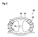
- FIG. 2 Another design option is the design with laminar conductive cores, as in FIG. 2 is shown.
- the figure shows a common mode push-pull reactor 100 having an outer core 102, an inner core 104 and a winding 106.
- the inner core 104 is closed by an air gap 108 and describes an eight.
- the outer core 102 forms or describes an oval.
- the winding 106 encloses both cores 102 and 104.
- FIG. 2 The arrangement and number of air gaps in FIG. 2 is selected by way of example and shows an arrangement with an air gap. Of course, other air gaps distributed over the magnetic path of the push-pull choke can be arranged.
- FIG. 3 shows a three-phase variant of a common-mode push-pull throttle, which is designated overall by the reference numeral 140.
- the illustration shows an outer core 142, an inner core 144, a first winding 146, a second winding 148, and a third winding 150.
- the presented common-mode push-pull choke is particularly suitable for use in single-phase and three-phase multi-string photovoltaic inverters.
- DC voltage is converted into alternating voltage and vice versa, and in which jumping potentials or a so-called CommonModeCurrent are to be prevented.
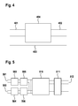
- FIG. 4 shows the potentials of an inverter 404, wherein the ground potential 403 is present as a possible reference potential on both the DC side and on the Konsdorfnseite.
- the potentials 402 of the conductors on the Kiruccinsei te can also be used as a reference potential in a Erdzug of the power grid.
- the potentials 401 of the DC side are usually capacitively coupled to the ground potential 403 and therefore may only have continuous values relative to the ground potential.
- FIG. 5 shows the basic arrangement of the common-mode and push-pull reactors of an inverter with multiple DC inputs.
- Reference numeral 501 denotes a first constant-value input with a first CMDM inductor 503 for smoothing and a first DC / DC adjuster 505 and reference numeral 502 a possible further constant-value input with a further CMDM inductor 504 and a further DC / DC adjuster 506 designated.
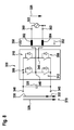
- FIG. 6 shows an embodiment of an inverter in an arrangement of the CMDM throttle 605 on the Kirdorfnseite 606.
- the DC / AC adjuster 604 converts the DC 601 into an alternating size.
- the inverter also includes a DC controller at the DC input, which consists of a DM reactor 602 and a Gleichehrnsteller 603.
- FIG. 7 shows the basic course of voltages in a single-phase inverter with H4 bridge and active freewheel, which also has a CMDM throttle. Based on the basic representation in FIG. 1 shows FIG. 7 in the first diagram 250 the course of a typical 230V mains voltage 40 at the terminals 42 and 44. The voltage curve at terminal 14 relative to the potential of the node 48 is sketched in the second diagram 252.
- the voltage curve is shown at terminal 16, again referred to the node 48. Both voltage waveforms are shown for a DC link voltage of 400V and also correspond to the switching states for the Switch 50 (negates for 56) for port 14 and 52 (and negates 54) for port 16.
- the voltage profile at the terminals 14 and 16 corresponds to averaged over a switching period of the output AC voltage (arrow 40) and is outlined in the sixth diagram 260. Based on the neutral or mains connection 44, the average voltage of terminals 14 and 16 corresponds to half the mains voltage (arrow 40).
- the mid-voltage jumps shown in the fourth graph 256 are received by the common mode choke with the coils 20 and 22 so that only a small magnetizing current builds up in the common mode choke, even when a freewheeling state is switched.
- the fifth graph 258 shows the voltage on a DM choke.
- the jumping of the potentials for example, at a photovoltaic generator can be prevented by the switching in the 20 kHz range or reduced to a fluctuation with the mains voltage. It thus remains the fluctuation with the mains voltage (50 Hz), as it can be seen in the absence of switching.
- FIG. 8 Figure 4 shows a standard H4 bridge 300 having a symmetrically distributed output inductor L1 302 and L2 304.
- the H4 bridge 300 includes a first switch S1 306, a second switch S2 308, a third switch S3 310, and a fourth switch S4 312. Further the illustration shows a capacitor C1 320 and a network 322.
- the mains voltage U Netz is indicated by an arrow 326.
- a further arrow 328 illustrates the voltage U a1 , an arrow 330 the voltage U ZK , an arrow 332 the voltage U a2 .
- a terminal a1 340, a terminal a2 342 and a terminal k1 344 and a terminal k2 346 is shown. Via the inductance L1 302, the voltage U L (arrow 350) drops as well as above the inductance L2 304 (arrow 352). Ports on network 322 are n1 360 and n2 362.
Landscapes
- Engineering & Computer Science (AREA)
- Power Engineering (AREA)
- Inverter Devices (AREA)
- Semiconductor Integrated Circuits (AREA)
Applications Claiming Priority (1)
| Application Number | Priority Date | Filing Date | Title |
|---|---|---|---|
| DE201310211121 DE102013211121A1 (de) | 2013-06-14 | 2013-06-14 | Wechselrichter |
Publications (2)
| Publication Number | Publication Date |
|---|---|
| EP2814151A2 true EP2814151A2 (fr) | 2014-12-17 |
| EP2814151A3 EP2814151A3 (fr) | 2015-04-01 |
Family
ID=50819603
Family Applications (1)
| Application Number | Title | Priority Date | Filing Date |
|---|---|---|---|
| EP20140170024 Ceased EP2814151A3 (fr) | 2013-06-14 | 2014-05-27 | Onduleur |
Country Status (2)
| Country | Link |
|---|---|
| EP (1) | EP2814151A3 (fr) |
| DE (1) | DE102013211121A1 (fr) |
Cited By (5)
| Publication number | Priority date | Publication date | Assignee | Title |
|---|---|---|---|---|
| CN104660088A (zh) * | 2015-03-04 | 2015-05-27 | 王曙光 | 光伏发电变频逆变系统 |
| DE202016104544U1 (de) | 2016-08-18 | 2016-09-29 | Schneefuß + Rohde GmbH | Mehrphasige Gegentakt-Leistungsdrossel |
| DE102017222664A1 (de) | 2017-12-13 | 2019-06-13 | Robert Bosch Gmbh | Gleichtakt-Gegentakt-Drossel für ein elektrisch betreibbares Kraftfahrzeug |
| DE102019122243A1 (de) * | 2019-08-19 | 2021-02-25 | Schmidbauer Transformatoren und Gerätebau GmbH | Stromwandlungssystem |
| WO2022033635A1 (fr) * | 2020-08-12 | 2022-02-17 | innolectric AG | Transformateur à résonance comportant une inductance couplée supplémentaire pour un dispositif de charge de bord (obc) |
Citations (4)
| Publication number | Priority date | Publication date | Assignee | Title |
|---|---|---|---|---|
| DE102004030912B3 (de) | 2004-06-25 | 2006-01-19 | Sma Technologie Ag | Verfahren zum Umwandeln einer elektrischen Gleichspannung einer Gleichspannungsquelle, insbesondere einer Photovoltaik-Gleichspannungsquelle in eine Wechselspannung |
| EP1861914B1 (fr) | 2005-10-24 | 2008-12-03 | Conergy AG | Onduleur |
| EP1369985B1 (fr) | 2002-05-15 | 2009-05-13 | Fraunhofer-Gesellschaft zur Förderung der angewandten Forschung e.V. | Onduleur pour transformer une tension continue en courant alternatif ou en tension alternative |
| DE102009029387A1 (de) | 2009-09-11 | 2011-03-24 | Robert Bosch Gmbh | DC-AC-Wechselrichteranordnung, insbesondere Solarzelleninverter |
Family Cites Families (2)
| Publication number | Priority date | Publication date | Assignee | Title |
|---|---|---|---|---|
| US6617814B1 (en) * | 2001-04-11 | 2003-09-09 | Rockwell Automation Technologies, Inc. | Integrated DC link choke and method for suppressing common-mode voltage in a motor drive |
| ES2718807T3 (es) * | 2012-06-07 | 2019-07-04 | Abb Research Ltd | Procedimiento de amortiguación de secuencia cero y equilibrado de tensión en un convertidor de tres niveles con condensadores de enlace de CC divididos y filtro LCL virtualmente conectado a tierra |
-
2013
- 2013-06-14 DE DE201310211121 patent/DE102013211121A1/de not_active Withdrawn
-
2014
- 2014-05-27 EP EP20140170024 patent/EP2814151A3/fr not_active Ceased
Patent Citations (4)
| Publication number | Priority date | Publication date | Assignee | Title |
|---|---|---|---|---|
| EP1369985B1 (fr) | 2002-05-15 | 2009-05-13 | Fraunhofer-Gesellschaft zur Förderung der angewandten Forschung e.V. | Onduleur pour transformer une tension continue en courant alternatif ou en tension alternative |
| DE102004030912B3 (de) | 2004-06-25 | 2006-01-19 | Sma Technologie Ag | Verfahren zum Umwandeln einer elektrischen Gleichspannung einer Gleichspannungsquelle, insbesondere einer Photovoltaik-Gleichspannungsquelle in eine Wechselspannung |
| EP1861914B1 (fr) | 2005-10-24 | 2008-12-03 | Conergy AG | Onduleur |
| DE102009029387A1 (de) | 2009-09-11 | 2011-03-24 | Robert Bosch Gmbh | DC-AC-Wechselrichteranordnung, insbesondere Solarzelleninverter |
Cited By (7)
| Publication number | Priority date | Publication date | Assignee | Title |
|---|---|---|---|---|
| CN104660088A (zh) * | 2015-03-04 | 2015-05-27 | 王曙光 | 光伏发电变频逆变系统 |
| DE202016104544U1 (de) | 2016-08-18 | 2016-09-29 | Schneefuß + Rohde GmbH | Mehrphasige Gegentakt-Leistungsdrossel |
| WO2018033451A1 (fr) | 2016-08-18 | 2018-02-22 | Manfred Schmelzer Gmbh | Bobine de puissance symétrique à multiples phases |
| DE102017222664A1 (de) | 2017-12-13 | 2019-06-13 | Robert Bosch Gmbh | Gleichtakt-Gegentakt-Drossel für ein elektrisch betreibbares Kraftfahrzeug |
| WO2019115207A1 (fr) | 2017-12-13 | 2019-06-20 | Robert Bosch Gmbh | Bobine en mode commun et en mode différentiel pour un véhicule à moteur pouvant fonctionner électriquement |
| DE102019122243A1 (de) * | 2019-08-19 | 2021-02-25 | Schmidbauer Transformatoren und Gerätebau GmbH | Stromwandlungssystem |
| WO2022033635A1 (fr) * | 2020-08-12 | 2022-02-17 | innolectric AG | Transformateur à résonance comportant une inductance couplée supplémentaire pour un dispositif de charge de bord (obc) |
Also Published As
| Publication number | Publication date |
|---|---|
| DE102013211121A1 (de) | 2014-12-18 |
| EP2814151A3 (fr) | 2015-04-01 |
Similar Documents
| Publication | Publication Date | Title |
|---|---|---|
| EP2737618B1 (fr) | Système de convertisseur électrique | |
| EP2750920B1 (fr) | Procédé et dispositif pour charger une batterie d'un mécanisme d'entraînement électrique en utilisant des composants du mécanisme d'entraînement électrique | |
| EP2027647B1 (fr) | Dispositif d'alimentation électrique dans un réseau d'alimentation électrique et convertisseur de tension continue destiné à un tel dispositif | |
| EP1369985B1 (fr) | Onduleur pour transformer une tension continue en courant alternatif ou en tension alternative | |
| EP2030299B1 (fr) | Onduleur destiné à injecter de l'énergie électrique dans un réseau de distribution d'énergie | |
| EP2815497B1 (fr) | Dispositif d'alimentation réseau, système d'alimentation en énergie et procédé de fonctionnement d'un disposif d'alimentation réseau | |
| AT505801B1 (de) | Verfahren zum betrieb eines elektronisch gesteuerten wechselrichters | |
| EP2863528B1 (fr) | Utilisation d'un onduleur comme un convertisseur CC/CC | |
| DE102007038959A1 (de) | Wechselrichter | |
| EP2623363B1 (fr) | Dispositif et procédé de chargement d'une batterie de traction d'un véhicule électrique | |
| WO2012168338A2 (fr) | Convertisseur survolteur | |
| EP2814151A2 (fr) | Onduleur | |
| DE102007038960A1 (de) | Wechselrichter | |
| EP2764614B1 (fr) | Onduleur multiniveau avec une pluralité des sous-modules onduleur pour la génération des tensions polyphasées | |
| EP2709257A2 (fr) | Circuit de convertisseur de courant et procédé de commande du circuit de convertisseur de courant | |
| EP2845303B1 (fr) | Convertisseur et procédés de conversion de tension | |
| WO2016066484A2 (fr) | Onduleur et bobine de réactance pour supprimer des bruitages en mode commun | |
| EP2421135B1 (fr) | Onduleur sans transformateur avec convertisseur abaisseur | |
| EP2582030A2 (fr) | Circuit avec onduleur | |
| DE102014203404A1 (de) | Stromrichterschaltung und Verfahren zum Betreiben derselben | |
| DE102020111355A1 (de) | Ladevorrichtung und Verfahren zum Laden eines elektrischen Energiespeichers eines elektrisch betriebenen Fahrzeugs mittels eines Gleichspannungswandlers, welcher verschiedene Betriebsmodi aufweist | |
| DE102008050765A1 (de) | Wechselrichteranordnung zum Einspeisen von photovoltaisch gewonnener Energie in ein öffentliches Netz | |
| EP2221952A2 (fr) | Hacheur bidirectionnel et système | |
| DE102013212692A1 (de) | Energiespeichereinrichtung mit Gleichspannungsversorgungsschaltung | |
| DE102011083645A1 (de) | Batterie-Ladegerät |
Legal Events
| Date | Code | Title | Description |
|---|---|---|---|
| 17P | Request for examination filed |
Effective date: 20140527 |
|
| AK | Designated contracting states |
Kind code of ref document: A2 Designated state(s): AL AT BE BG CH CY CZ DE DK EE ES FI FR GB GR HR HU IE IS IT LI LT LU LV MC MK MT NL NO PL PT RO RS SE SI SK SM TR |
|
| AX | Request for extension of the european patent |
Extension state: BA ME |
|
| PUAI | Public reference made under article 153(3) epc to a published international application that has entered the european phase |
Free format text: ORIGINAL CODE: 0009012 |
|
| PUAL | Search report despatched |
Free format text: ORIGINAL CODE: 0009013 |
|
| AK | Designated contracting states |
Kind code of ref document: A3 Designated state(s): AL AT BE BG CH CY CZ DE DK EE ES FI FR GB GR HR HU IE IS IT LI LT LU LV MC MK MT NL NO PL PT RO RS SE SI SK SM TR |
|
| AX | Request for extension of the european patent |
Extension state: BA ME |
|
| RIC1 | Information provided on ipc code assigned before grant |
Ipc: H02M 1/00 20070101AFI20150226BHEP |
|
| R17P | Request for examination filed (corrected) |
Effective date: 20151001 |
|
| RBV | Designated contracting states (corrected) |
Designated state(s): AL AT BE BG CH CY CZ DE DK EE ES FI FR GB GR HR HU IE IS IT LI LT LU LV MC MK MT NL NO PL PT RO RS SE SI SK SM TR |
|
| RAP1 | Party data changed (applicant data changed or rights of an application transferred) |
Owner name: SMA SOLAR TECHNOLOGY AG |
|
| STAA | Information on the status of an ep patent application or granted ep patent |
Free format text: STATUS: EXAMINATION IS IN PROGRESS |
|
| 17Q | First examination report despatched |
Effective date: 20190423 |
|
| STAA | Information on the status of an ep patent application or granted ep patent |
Free format text: STATUS: EXAMINATION IS IN PROGRESS |
|
| STAA | Information on the status of an ep patent application or granted ep patent |
Free format text: STATUS: EXAMINATION IS IN PROGRESS |
|
| STAA | Information on the status of an ep patent application or granted ep patent |
Free format text: STATUS: THE APPLICATION HAS BEEN REFUSED |
|
| 18R | Application refused |
Effective date: 20230310 |