EP2814034B1 - Vorrichtung und Verfahren zum Löschen von in einer Speichervorrichtung gespeicherten Daten - Google Patents
Vorrichtung und Verfahren zum Löschen von in einer Speichervorrichtung gespeicherten Daten Download PDFInfo
- Publication number
- EP2814034B1 EP2814034B1 EP14170409.8A EP14170409A EP2814034B1 EP 2814034 B1 EP2814034 B1 EP 2814034B1 EP 14170409 A EP14170409 A EP 14170409A EP 2814034 B1 EP2814034 B1 EP 2814034B1
- Authority
- EP
- European Patent Office
- Prior art keywords
- circuitry
- signal
- erase
- asserted
- control signal
- Prior art date
- Legal status (The legal status is an assumption and is not a legal conclusion. Google has not performed a legal analysis and makes no representation as to the accuracy of the status listed.)
- Active
Links
Images










Classifications
-
- G—PHYSICS
- G11—INFORMATION STORAGE
- G11C—STATIC STORES
- G11C7/00—Arrangements for writing information into, or reading information out from, a digital store
- G11C7/24—Memory cell safety or protection circuits, e.g. arrangements for preventing inadvertent reading or writing; Status cells; Test cells
-
- G—PHYSICS
- G11—INFORMATION STORAGE
- G11C—STATIC STORES
- G11C16/00—Erasable programmable read-only memories
- G11C16/02—Erasable programmable read-only memories electrically programmable
- G11C16/06—Auxiliary circuits, e.g. for writing into memory
- G11C16/22—Safety or protection circuits preventing unauthorised or accidental access to memory cells
-
- G—PHYSICS
- G11—INFORMATION STORAGE
- G11C—STATIC STORES
- G11C8/00—Arrangements for selecting an address in a digital store
- G11C8/20—Address safety or protection circuits, i.e. arrangements for preventing unauthorized or accidental access
-
- G—PHYSICS
- G11—INFORMATION STORAGE
- G11C—STATIC STORES
- G11C7/00—Arrangements for writing information into, or reading information out from, a digital store
- G11C7/22—Read-write [R-W] timing or clocking circuits; Read-write [R-W] control signal generators or management
Definitions
- the present invention relates to an apparatus and method for erasing data stored within a memory device.
- a typical memory device comprising an array of memory cells arranged in rows and columns
- data remanence may be observed since such a memory device often retains its last stored value even after the processing device using that memory device has no further need for that stored value, and hence the memory cells storing that value are available for overwriting with new data. Only once those memory cells have actually been overwritten with new data will the old data no longer be available in the memory device.
- one known approach often referred to as a cold boot attack, involves turning off the system incorporating the memory device and associated processing device, and then turning it on again.
- This allows the software protection measure to be circumvented. Under normal conditions, this would not be a problem, as removing the power supply to the memory device would typically result in the stored data being lost.
- special, external, conditions are applied, this providing another form of data remanence.
- One example of such a special external condition is to subject the memory device to a low temperature before removing the power. Under such conditions, once the power is restored, the software protection will have been circumvented, and the data may still be extracted from the memory device.
- US 7,570,532 describes a memory device that includes memory cells that are overwritten in response to receipt of a clear request signal and an overwrite value.
- the clear request signal enables all word lines of the memory device to be overwritten, and delay elements are used to cause the overwrite value to be written into each column of memory cells at different times, in order to reduce the instantaneous current.
- the clear request signal can be issued in response to a condition such as a change in system clock frequency.
- EP 1,542,180 A1 describes an electronic data processing device including an access protected memory for storing secure data, the device including a tampering detection and protection circuit for detecting a tamper condition, and for generating a tamper signal upon detection of said tamper condition, upon receipt of said tamper signal a tampering sequencer being arranged to generate a series of clock pulses and to erase, under control of that series of clock pulses, the secure data stored in the access protected memory.
- WO 2008/150939 describes a method and device for protecting information contained in an integrated circuit, where a test controller state machine (TCSM) is used to monitor the state of the data storage device and, upon assertion of a test request, to cause the contents of the data storage device to be erased, the TCSM preventing access to the data storage device until it has confirmed that the data has been erased.
- TCSM test controller state machine
- GB 2,460,213A describes a semiconductor device comprising a memory cell array that is managed on a sector basis, a first latch circuit which includes sub-circuits for latching activation information on a sector, decoding an address and outputting the latched activation information, and a second latch circuit which includes sub-circuits for storing erase information on a sector, decoding a common address and outputting the latched information.
- the present invention provides an apparatus comprising: a memory device comprising an array of memory cells, and configured to operate from a clock signal; erase circuitry, responsive to receipt of an erase signal in an asserted state, to perform a forced write operation independently of the clock signal in respect of each memory cell within a predetermined erase region of said array; and erase signal generation circuitry configured to receive a control signal and to maintain said erase signal in a deasserted state provided that the control signal takes the form of a pulse signal having at least a predetermined minimum frequency between pulses; the erase signal generation circuitry being configured to issue said erase signal in said asserted state if the control signal is removed or if the control signal does not take the form of said pulse signal; wherein: said erase signal generation circuitry comprises capacitor circuitry, and output circuitry configured to generate the erase signal in dependence on an output from the capacitor circuitry; the capacitor circuitry being configured to switch between a charging operation and a discharging operation dependent on the control signal; if the control signal is removed or if the control
- erase circuitry is provided in association with the memory device, that is responsive to an asserted erase signal, to perform a forced write operation independently of the clock signal received by the memory device, the forced write operation being performed in respect of each memory cell within a predetermined erase region of the memory array.
- erase signal generation circuitry is configured to generate the erase signal dependent on a received control signal, such that if the control signal takes the form of a pulse signal having at least a predetermined minimum frequency between pulses, the erase signal is maintained in a de-asserted state, but whenever the control signal does not take that form, the erase signal is then asserted to cause the forced write operation to take place.
- Such an approach enables the security of a memory device to be improved, and in particular prevents hackers from taking advantage of the earlier mentioned data remanence effects, by ensuring that stored data is overwritten in an efficient, and clock independent, manner, triggered by assertion of an erase signal generated if a pulse-based control signal does not take it is expected form. Since the forced write operation occurs independently of the clock signal, once the erase signal has been asserted a hacker will be unable to prevent the forced write operation taking place merely by seeking to remove the clock signal from the memory device.
- the predetermined erase region can take a variety of forms. For example, it may be chosen to be the entire memory array, or instead could be chosen to be a predetermined area of the array in which certain secure data is stored, for example encryption keys or parts of encryption keys, decipher results, etc.
- the predetermined erase region may occupy one or more rows of the memory array, and/or may occupy one or more columns of the memory array.
- the predetermined erase region is defined, the above described mechanism provides a particular efficient technique for erasing the data in that region.
- each entry in the tag array typically comprises a valid bit to identify whether the corresponding cache line in the data array is valid or not.
- each of the valid bits needs to be cleared, and typically this will involve issuing a separate write operation in respect of every tag entry, hence taking a significant amount of time to perform.
- a predetermined erase region can be defmed to include the column of the array containing the valid flags for every tag entry, and when it is necessary to reset the cache, an asserted erase signal can be issued to cause the above described erase functionality to write the relevant bit value into each of the valid flags to identify those entries as being invalid (typically this involving writing a logic zero value into each of the valid flag positions).
- the erase signal generation circuitry comprises capacitor circuitry, and output circuitry configured to generate the erase signal in dependence on an output from the capacitor circuitry.
- the capacitor circuitry is configured to switch between a charging operation and a discharging operation dependent on the control signal, and the output circuitry is configured to generate the erase signal in said asserted state if the output from the capacitor circuitry reaches a predetermined activation voltage level. Further, if the control signal takes the form of said pulse signal the output from the capacitor circuitry is configured not to reach said predetermined activation voltage level, thereby causing the erase signal to be maintained in said de-asserted state.
- the control signal includes regular pulses having at least the predetermined minimum frequency
- the switching between the charging and discharging operations of the capacitor circuitry will be such that the output from the capacitor circuitry does not reach the predetermined activation voltage level.
- the control signal is tampered with so as to prevent such pulses, or reduce the frequency of those pulses below the above-mentioned predetermined minimum frequency, then the output from the capacitor circuitry will reach the predetermined activation voltage level, and trigger assertion of the erase signal.
- the predetermined activation voltage level may be a voltage level that the capacitor circuitry discharges to in the absence of the regular control signal, or a voltage level that the capacity circuitry charges to in the absence of the regular control signal.
- the predetermined activation voltage level is a voltage level that the capacity circuitry charges to in the absence of the regular control signal, and the capacitor circuitry is configured to perform said charging operation whenever the control signal does not contain a pulse, and to switch to said discharging operation for the duration of each pulse in said control signal.
- it is the presence of the regular pulses at at least the predetermined minimum frequency that stops the capacitor charging up to the predetermined activation voltage level.
- the erase signal generation circuitry comprises a current controlled inverter circuit configured to provide an input to the capacitor circuitry in dependence on the control signal.
- a current controlled inverter circuit configured to provide an input to the capacitor circuitry in dependence on the control signal.
- the apparatus further comprises bias voltage generation circuitry configured to generate a bias voltage provided to at least one component within the current controlled inverter circuitry to control a rate at which the voltage level of the output of the capacitor circuitry changes during at least one of said charging operation and said discharging operation.
- the current controlled inverter circuitry is configured to use the bias voltage to control the rate at which the voltage level of the output of the capacitor circuitry changes during the charging operation, the charging operation taking place when a pulse is not present in the control signal.
- control signal input to the erase signal generation circuitry can be generated in a variety of ways.
- the apparatus further comprises control signal generation circuitry configured to generate the control signal input to the erase signal generation circuitry, the control signal generation circuitry comprising edge detector circuitry configured to receive an input signal and to generate a pulse within said control signal each time the input signal changes state between first and second voltage levels.
- control signal generation circuitry configured to generate the required pulses within the control signal, this avoids the designer of the apparatus having to separately generate the control signal with the required specific pulses expected by the erase signal generation circuitry, and instead the developer merely needs to generate an input signal which changes state between the first and second voltage levels at at least the earlier mentioned predetermined minimum frequency. Each such transition in state of the input signal will then cause the required pulse signal to be inserted in the control signal.
- the edge detector circuitry can be constructed in a variety of ways, but in one embodiment comprises delay circuitry configured to generate a delayed input signal, and comparison circuitry configured to generate each said pulse dependent on a comparison between said input signal and said delayed input signal. This provides a particularly efficient mechanism for generating the required pulses, and in one embodiment the delay introduced by said delay circuitry determines a width of each pulse generated by the edge detector circuitry.
- bias voltage generation circuitry is configured to generate a bias voltage provided to at least one component within the delay circuitry in order to control said delay introduced by said delay circuitry. As a result, this enables the width of the pulse is generated by the edge detector circuitry to be tuned, dependent on the bias voltage produced by the bias voltage generation circuitry.
- control signal generation circuitry further comprises pulse override circuitry configured, on detection of at least one predetermined condition, to prevent the control signal from taking the form of said pulse signal irrespective of the output of the edge detector circuitry, to thereby cause the erase signal generation circuitry to issue said erase signal in said asserted state.
- the predetermined condition can be specified to take account of a variety of situations where it may be desirable to assert the erase signal irrespective of the output from the edge detector circuitry.
- the at least one predetermined condition comprises a condition indicating potential tampering with the input signal provided to the edge detector circuitry.
- a hacker could seek to modify the input signal in a way that ensures that the edge detector circuitry continues to generate pulses within the control signal at the required interval to prevent the erase signal being asserted, in situations where the normal, untampered, input signal would cause the edge detector circuitry to generate a control signal causing the erase signal to be asserted.
- a hacker may seek to take a clock signal present within the apparatus and apply it as the input signal, and provided that clock signal was of a suitable frequency, this could cause the edge detector circuitry to continue to insert pulses within the control signal at the required interval to prevent the erase signal being asserted.
- the pulse override circuitry may comprise frequency comparator circuitry configured to detect if the input signal has the same frequency as a clock signal supplied to said frequency comparator circuitry (for example a system clock, or the clock signal used to operate the memory device (often the same frequency as the system clock but shifted in time)), and in that event to prevent the control signal from taking the form of said pulse signal irrespective of the output of the edge detector circuitry.
- a clock signal supplied to said frequency comparator circuitry for example a system clock, or the clock signal used to operate the memory device (often the same frequency as the system clock but shifted in time)
- this will cause the erase signal to be asserted, and accordingly cause the predetermined erase region of the array to be subjected to the forced write operation in order to overwrite any currently stored data in that region.
- the frequency comparator circuitry can take a variety of forms, but in one embodiment comprises a first flip flop circuit and a second flip flop circuit, both the first and second flip flop circuits being configured to receive said input signal, and being operated such that on a rising edge of a received clock signal the first flip flop circuit outputs a current value of the input signal received by the first flip flop circuit, and on a falling edge of the received clock signal the second flip flop outputs an inverted version of the current value of the input signal received by the second flip flop circuit.
- the outputs from both the first and second flip flop circuits are subjected to a logical XOR operation in order to generate an output from the frequency comparator circuitry. Accordingly, if the input signal is merely created from the clock signal, the output from the frequency comparator circuitry will be at logic zero value, whereas if the input signal is in fact generated separately to the clock signal, and accordingly has a different frequency, the output from the frequency comparator circuitry will predominately be at a logic one value.
- the apparatus further comprises logical AND circuitry configured to receive the output from the edge detector circuitry and the output from the pulse override circuitry and to perform a logical AND operation in order to generate said control signal, the pulse override circuitry being configured to generate a logic 1 output value in the absence of said at least one predetermined condition, but being configured to generate a logic 0 output value whilst said at least one predetermined condition is detected.
- the pulse override circuitry being configured to generate a logic 1 output value in the absence of said at least one predetermined condition, but being configured to generate a logic 0 output value whilst said at least one predetermined condition is detected.
- the erase circuitry can be configured in a variety of ways.
- the array of memory cells is arranged as a plurality of rows and columns, each row of memory cells being coupled to an associated word line, and each column of memory cells being coupled to an associated at least one bit line
- the apparatus further comprises: decoder circuitry configured to be responsive to a write operation to decode an address indication associated with the write operation in order to determine the row containing addressed memory cells for the write operation, and to issue, in dependence on said clock signal, an asserted word line signal on the associated word line for the determined row; and write circuitry configured to be responsive to said write operation to control a voltage level of the associated at least one bit line for each of said addressed memory cells to cause write data to be written into said addressed memory cells.
- the erase circuitry may comprise the decoder circuitry and the write circuitry, the decoder circuitry being configured to be responsive to said asserted erase signal to issue, independently of said clock signal, said asserted word line signal on the word line associated with each row in said predetermined erase region, and the write circuitry being configured to be responsive to said asserted erase signal to control the voltage level of the associated at least one bit line for each memory cell in said predetermined erase region, in order to cause erase write data to be written into the memory cells of said predetermined erase region.
- the normal operation of the decoder circuitry and write circuitry is modified upon receipt of an asserted erase signal.
- the decoder circuitry will typically assert a word line signal on a single word line associated with the row that contains the addressed memory cells for the write operation.
- the decoder circuitry issues an asserted word line signal on the word line associated with each row in a predetermined erase region of the array. Hence, if that predetermined erase region occupies multiple rows of the array, this will result in multiple word lines being activated.
- the decoder circuitry is configured to issue such asserted word line signals independently of the clock signal.
- the write circuitry is then configured to be responsive to the asserted erase signal to control the voltage level on at least one bit line for each memory cell in the predetermined erase region, in order to cause erase write data to be written into the memory cells of the predetermined erase region.
- the erase write data can take a variety of forms. In some embodiments that erase write data may be predetermined, whilst in other embodiments such erase write data is instead generated randomly, or the write circuitry is used to merely write into the memory device the data currently present at the input pins of the memory device. Whatever the form of the erase write data, it will be used to positively overwrite the current data stored in the predetermined erase region. As a result, it can be seen that by such a mechanism the asserted erase signal is used to trigger a forced write operation in respect of each memory cell within the predetermined erase region in a clock independent manner.
- the above-described mechanism provides a particularly efficient technique for erasing the data in that region, since it avoids the need for a separate write operation to be issued under software control for each row within the predetermined erase region.
- the decoder circuitry in response to the asserted erase signal, automatically asserts word line signals in respect of every row in the predetermined erase region. These word line signals can be asserted in parallel, and the same erase write data is written into every row within the predetermined erase region.
- the decoder circuitry and write circuitry are configured to be responsive to the asserted erase signal independent of a current operating state of the memory device at a time the erase signal is asserted.
- the current operating state may be any powered state of the memory device, and hence for example the memory device may be in a read state where it is performing a read operation, a write state where it is performing a write operation, an idle state where it is currently performing no operation, or a non-enabled state (for example where a chip enable signal is de-asserted in order to deselect the memory device).
- the decoder circuitry and write circuitry will still operate in response to that asserted erase signal to perform the forced write operation discussed earlier in order to write erase write data into each memory cell of the predetermined erase region.
- the decoder circuitry can take a variety of forms. However, in one embodiment the decoder circuitry comprises first stage decoding circuitry configured to generate a plurality of intermediate signals in response to the address indication, and further stage decoding circuitry configured to generate the asserted word line signal in dependence on values of the intermediate signals. The decoder circuitry is then configured to be responsive to the asserted erase signal to set the intermediate signals to values which will cause the further stage decoding circuitry to then issue the asserted word line signal on the word line associated with each row in the predetermined erase region.
- the decoder circuitry modifies its behaviour upon receipt of the asserted erase signal by manipulating the intermediate signals generated by the first stage decoding circuitry.
- the decoder circuitry is then able to deviate from its normal operation that would restrict it to asserting only a single word line signal at any point in time, to instead be able to assert multiple word line signals at a time.
- the required modification to the decoder circuitry could instead have been implemented in the further stage decoding circuitry, it has been found that a particularly efficient and low transistor count solution can be achieved by instead modifying the behaviour of the first stage decoding circuitry, and in particular the manner in which the intermediate signals are set by that first stage decoding circuitry.
- the circuits implementing the first stage decoding circuitry are typically very small compared with the circuits required to implement the further stage decoding circuitry, and are repeated only a small number of times even for relatively large sized memory devices.
- this can provide an extra level of secrecy, since the low transistor count makes the added circuitry very difficult to detect by hackers.
- the decoder circuitry can be arranged to issue asserted word line signals independently of the clock signal when it is operating in response to the asserted erase signal.
- timing of operation of the further stage decoding circuitry is controlled by the clock signal, and the decoder circuitry is responsive to the asserted erase signal to control the timing of operation of the further stage decoding circuitry independently of said clock signal.
- the operating of the further stage decoding circuitry is modified so that its operation is clock independent.
- the decoder circuitry further comprises clock generation circuitry configured, in the absence of the asserted erase signal, to generate an internal clock signal from the clock signal and to provide the internal clock signal to the further stage decoding circuitry.
- the clock generation circuitry is then responsive to the asserted erase signal to assert the internal clock signal at a predetermined value independent of the clock signal, the further stage decoding circuitry being responsive to the internal clock signal asserted at that predetermined value to generate the asserted word line signal in dependence on the values of the intermediate signals.
- the internal clock signal is effectively deactivated in the presence of the asserted erase signal and replaced by the asserted predetermined value in order to trigger assertion of the necessary word line signals as dictated by the values of the intermediate signals.
- the first stage decoding circuitry comprises a plurality of intermediate signal generation blocks, each intermediate signal generation block being configured to receive a plurality of bits derived from the address indication and to generate, in dependence on the plurality of bits, an associated intermediate signal forming one of the plurality of intermediate signals.
- at least a subset of the intermediate signal generation blocks are configured to set their intermediate signal to a predetermined value irrespective of the received plurality of bits.
- each intermediate signal generation block within the above-mentioned subset can be configured to set its intermediate signal to a predetermined value.
- each intermediate signal generation block is configured, in the absence of the asserted erase signal, to implement a NAND gate function in order to derive the associated intermediate signal from the received plurality of bits.
- the at least a subset of the intermediate signal generation blocks are configured to override the NAND gate function in order to set their associated intermediate signal to the predetermined value irrespective of the received plurality of bits.
- the NAND gate function receives as it inputs a plurality of bit values, then only if all of those bit values are one will the NAND gate function output a logic zero value.
- the signal generation block in the presence of the asserted erase signal, is modified so that it outputs as the predetermined value a logic zero value irrespective of the received plurality of bits. This means that many more intermediate signal generation blocks can be arranged to output logic zero values than would be the case during a normal write operation, and this in turn allows multiple asserted word line signals to be issued at the same time in response to the asserted erase signal.
- each such intermediate signal generation block comprises a first transistor circuit configured to drive an output of that intermediate signal generation block to the predetermined value in the presence of the asserted erase signal.
- the predetermined value is a logic zero value
- multiple of the intermediate signal generation blocks that are configured to override their NAND gate function can be configured to share a second transistor circuit configured to decouple those multiple intermediate signal generation blocks from a supply voltage in the presence of the asserted erase signal.
- the second transistor circuit can take the form of a PMOS transistor coupling the NAND gate structure to the power supply, and driven by the erase signal. Accordingly, when the erase signal is asserted at a logic one value, the PMOS transistor is turned off, decoupling the NAND gate structure from the power supply.
- a PMOS transistor can be shared by them all, and each block only needs an NMOS transistor adding to it in order to implement the above functionality.
- the above described functionality can be achieved by the addition of nine transistors.
- each column of memory cells is coupled to an associated pair of bit lines, and the write circuitry is configured to be responsive to the asserted erase signal to control the voltage levels on the associated bit line pair for each memory cell in said predetermined erase region, such that for each bit line pair one bit line is at a logic 1 voltage level and the other bit line is at a logic 0 voltage level.
- the voltages on the bit line pairs can be arranged identically, so that the same value is written into every memory cell across each row, there is no requirement for the same value to be written into every memory cell, and the value can be set separately for each column by appropriate manipulation of the bit line voltages if desired.
- the write circuitry may be configured to be responsive to the asserted erase signal to control the voltage levels on the associated bit line pair for each memory cell in said predetermined erase region, such that for each bit line pair both bit lines are pulled to a voltage level different to a precharged voltage level of the bit lines, in order to cause random data to be written into the memory cells in the predetermined erase region.
- the precharge voltage level is a logic one level
- both bit lines may be pulled to the logic zero level during the forced write operation. This will effectively randomise the data written into the memory cells within the predetermined erase region, but still is an effective approach for ensuring that the previous contents of those memory cells are no longer available.
- the above-described modified behaviour of the decoder circuitry can result in potentially a large number of word lines being asserted at the same time. This can give rise to a large, and easily detectable, in-rush current as the multiple word line drivers within the decoder circuitry activate their corresponding word lines. Such a large draw of current could also potentially affect neighbouring logic around the memory device within a system-on-chip containing the memory device, if it is not well controlled.
- the operation of the decoder circuitry is further modified in order to limit the in-rush current.
- the decoder circuitry is configured to be responsive to the asserted erase signal to treat the word lines associated with the multiple rows within the predetermined erase region as forming a plurality of word line groups, and to stagger in time issuance of the asserted word line signal to the word lines in different word line groups in the plurality of word line groups. By staggering the time at which the word line signals are asserted, this reduces the in-rush current drawn by the word line drivers.
- this also allows the word lines to be activated more quickly, which in turn causes the writing of the addressed memory cells to occur more quickly, causing less crowbar current to be consumed within the memory cells. This in turn allows the size of the components within the write circuitry used to control the voltages on the bit lines to be reduced.
- the decoder circuitry can be configured to stagger in time the issuance of the asserted word line signals.
- the decoder circuitry comprises first stage decoding circuitry configured to generate a plurality of intermediate signals in response to the address indication, and further stage decoding circuitry configured to generate the asserted word line signal in dependence on values of the intermediate signals, and the decoder circuitry is configured to be responsive to the asserted erase signal to set the intermediate signals to values which will cause the further stage decoding circuitry to then issue the asserted word line signal on the word line associated with each row in said predetermined erase region.
- the decoder circuitry may be configured to be responsive to the asserted erase signal to stagger in time the setting of the intermediate signals to said values, in order to cause to be staggered in time the issuance of the asserted word line signal to the word lines in different word line groups in the plurality of word line groups.
- the decoder circuitry may be configured to be responsive to the asserted erase signal to stagger in time the setting of the intermediate signals to said values, in order to cause to be staggered in time the issuance of the asserted word line signal to the word lines in different word line groups in the plurality of word line groups.
- the first stage decoding circuitry comprises a plurality of intermediate signal generation blocks, and at least a subset of those intermediate signal generation blocks are configured, in the presence of the asserted erase signal, to set their intermediate signal to a predetermined value irrespective of the received plurality of bits
- the staggering of the generation of the intermediate signals can be achieved by providing delay circuitry within the decoder circuitry to differentially delay propagation of the asserted erase signal to the intermediate generation blocks in said at least a subset.
- the delay circuitry can be arranged in a variety of ways. For example, if the intermediate signal generation blocks are considered to form multiple intermediate signal generation groups, the delay circuitry may be configured to differentially delay propagation of the asserted erase signal to the intermediate generation blocks in at least one of those groups. In one particular embodiment, the delay circuitry may be configured to delay propagation of the asserted erase signal to one of the groups, whilst no such delay circuitry is included in the other groups. This allows sets of word lines to be activated at a time, whilst avoiding a situation where all of the required word lines are activated at the same time.
- the delay circuitry is configured to delay propagation of the asserted erase signal to every intermediate signal generation block in said at least one of said multiple intermediate signal generation groups.
- one intermediate signal generation block in each intermediate signal generation group will be preconditioned to generate the output value that will need to be generated by multiple of those intermediate signal generation blocks in the presence of the asserted erase signal.
- any intermediate signal generation group that is going to be subjected to the above-described delay mechanism there is no need initially to provide the erase signal to any of the intermediate signal generation blocks in that group, since there will be one arbitrary intermediate signal generation block in that group that is already producing the required output.
- this by delaying propagation of the asserted erase signal to all of the intermediate signal generation blocks in the relevant intermediate signal generation group, this further smooths the power consumption, and in particular ensures a predictable initial in-rush current when the erase signal is first asserted.
- the sizing of the components in the write driver circuitry needs to be such that when the write driver circuitry is controlling the voltages on the bit lines during the erase procedure, it can overcome any counteracting effect produced by the bit cells connected to the relevant column.
- the write driver circuitry may be seeking to write a first data value into every bit cell in the column, in a situation where every bit cell in the column currently stores a second, opposite, value. In that situation, the write driver circuitry components will need to be strong enough to overcome the counteractive effects that the bit cells will present on the bit lines.
- the above-described staggering mechanism can be adapted to assist the writing process, and hence reduce the size of the components required within the write circuitry.
- the decoder circuitry is configured to issue the asserted word line signal to the word lines in a first word line group and to defer issuance of the asserted word line signal to any further word line groups until the forced write operation has been completed in respect of the memory cells of the predetermined erase region that are associated with the first word line group.
- the present invention provides a method of operating an apparatus to erase data in a memory device comprising an array of memory cells and configured to operate from a clock signal, the method comprising: responsive to an erase signal in an asserted state, performing a forced write operation independently of the clock signal in respect of each memory cell within a predetermined erase region of said array; maintaining said erase signal in a deasserted state provided that a control signal takes the form of a pulse signal having at least a predetermined minimum frequency between pulses; and issuing said erase signal in said asserted state if the control signal is removed or if the control signal does not take the form of said pulse signal; wherein: said maintaining and issuing steps comprise generating the erase signal in dependence on an output from capacitor circuitry that is configured to switch between a charging operation and a discharging operation dependent on the control signal, such that if the control signal is removed or if the control signal does not take the form of said pulse signal, the output from the capacitor circuitry is configured to reach a predetermined activation voltage level
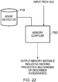
- the present invention provides a computer program storage medium storing a memory compiler computer program for controlling a computer to generate an instance of a memory device from a memory architecture associated with the memory compiler computer program, the memory architecture specifying a definition of circuit elements and data defining rules for combining those circuit elements, such that said instance generated specifies a memory device formed by the apparatus in accordance with the first aspect the present invention.
- FIG. 1 is a block diagram of an apparatus in accordance with one embodiment.
- a memory device 900 has uninterruptable fast memory erase circuitry 902 provided in association therewith.
- This erase circuitry 902 is responsive to receipt of an asserted erase signal over path 903, to perform a forced write operation independently of the clock signal 905 used to operate the memory device 900. Further, the forced write operation occurs in respect of every memory cell within a predetermined erase region of the memory array within the memory device 900. Hence, if a certain predetermined area of the memory is used to store sensitive data, such as encryption keys, that area could be set to be the predetermined erase region.
- the erase write data used to overwrite the contents of the predetermined erase region can take a variety of forms. In some embodiments it may be predetermined, whilst in other embodiments it can instead be generated randomly, or alternatively the data currently presented over path 907 may be written into the memory region. Whatever the form of the erase write data, it will be used to positively overwrite the current data stored in the predetermined erase region.
- the uninterruptable fast memory erase circuitry 902 can take a variety of forms, but in one embodiment can be constructed in accordance with one of the embodiments described later with reference to figures 13 to 21 . Further, whilst the predetermined erase region may be only a subset of the total memory array, it can alternatively be set to be the entire memory array, so that on assertion of the erase signal over path 903, the entire contents of the memory array are erased.
- the erase signal issued over path 903 can be generated in a variety of ways, however, in one embodiment "if-not timer" circuitry 904 is used that receives a control signal which is expected to take the form of a pulse signal having at least a predetermined minimum frequency between pulses, in the illustrative example it being assumed that a pulse will be received at least every ten microseconds. Whilst the control signal does take the form of such a pulse signal, the timer circuitry 904 does not assert the erase signal.
- the erase signal will be asserted over path 903, triggering the erase circuitry 902 to erase the data in the predetermined erase region of the memory array.
- pulse intrusion circuitry 906 can also be provided to detect situations where there may be a potential tampering of the input signal provided to the timer circuitry 904 in an attempt to simulate the required pulse signal in situations where the pulse signal would not naturally be produced.
- An example of such circuitry will be discussed in more detail later with reference to Figure 2B and Figure 9 .
- intrusion detection mechanisms 908 may also be provided for asserting an erase signal, and in the event that any such other intrusion detection mechanisms are provided, their outputs can be multiplexed by the circuitry 910 with the erase signal generated by the timer circuitry 904 in order to produce the erase signal input over path 903 to the erase circuitry 902.
- the presence of the erase circuitry 902 has no effect of the behaviour of the memory device 900, and accordingly data can be written into the memory device 900 over path 907, or read from the memory device over path 909, in accordance with the provided clock signal 905, in the standard manner.
- FIG. 2A is a block diagram illustrating components provided within the timer circuitry 904 of Figure 1 is accordance with one embodiment.
- a control signal is input to delay circuitry 912. Whilst the control signal takes the form of the earlier described pulse signal having at least a predetermined minimum frequency between the pulses, the output from the delay circuitry 912 will remain de-asserted, i.e. the erase signal will be in a de-asserted state. However, if a situation arises where the pulse signal is no longer present within the control signal, or its frequency drops below the predetermined minimum frequency, then this will trigger the delay circuitry 912 to assert the erase signal.
- edge detector circuitry 914 is arranged to generate the required control signal based on an input signal that is not required to contain pulses of the required width to causes correct operation of the delay circuitry.
- all that is required of the input signal to the edge detector circuitry is that that signal changes its logical state (i.e. from a logic 0 value to a logic 1 value or from a logic 1 value to a logic 0 value) with at least the predetermined minimum frequency at which pulses are required to be included in the control signal.
- a voltage bias generator 916 can be arranged to generate a bias voltage which can be provided to at least certain components within the edge detector 914 and/or the delay circuitry 912 in order to tune the operation of those circuits.
- the bias voltage can be used to tune the width of the pulses generated by the edge detector circuitry 914 and/or can be used to vary the rate of change of the voltage at the output of the delay circuitry during a charging or discharging operation of that delay circuitry, as will be discussed in more detail later.
- pulse intrusion circuitry 906 of Figure 1 in one embodiment can take the form of the frequency comparator circuitry 918 shown in Figure 2B .
- the frequency comparator circuitry 918 effectively provides a pulse override functionality, in that on detection of at least one predetermined condition (in the embodiment shown in Figure 2B this being a condition that the input signal to the edge detector circuitry 914 has the same frequency as the clock signal provided to the frequency comparator), it prevents the control signal from taking the form of the earlier described pulse signal, and accordingly causes the delay circuitry to assert the erase signal.
- the frequency comparator circuitry 918 is arranged in the embodiment of Figure 2B to output a logic one value, hence conditioning the AND gate 920 to output as the control signal the signal that it receives from the edge detector circuitry 914.
- the frequency comparator circuitry 918 detects that the frequency of the input signal to the edge detector 914 is the same as that of the clock signal, the output from the frequency comparator circuitry transitions to a logic 0 value, hence causing the control signal to take a logic 0 value irrespective of the output from the edge detector circuitry 914.
- the delay circuitry 912 will detect the absence of the pulses, and assert the erase signal.
- the additional provision of the frequency comparator provides a further level of robustness to attack.
- the frequency comparator could detect such a hacking attempt, and cause the erase signal to be asserted anyway.
- FIG 3 is a diagram illustrating components provided in one embodiment to implement the bias generator circuitry 916 of Figures 2A or 2B .
- the series of NMOS transistors 930, 932, 934 limit the current flow.
- the two PMOS transistors 925, 927 are sized differently and in particular in one embodiment the transistor 925 is arranged to be of the order of ten times bigger than the PMOS transistor 927, hence consuming more current.
- the small current that flows through the PMOS transistor 927 can then be replicated or even divided using a current mirror, a current mirror being achieved by connecting the output node to the gate of the PMOS transistor 927. Through such an arrangement, the output node will be at a voltage level which, when supplied to PMOS components within the edge detector circuitry 914 and/or the delay circuitry 912, will only partially turn on those PMOS transistors.
- FIG 4 illustrates components provided in one embodiment to implement the delay circuitry 912 of Figures 2A or 2B .
- a current controlled inverter circuit 950 is formed by the series of PMOS transistors 952, 954, 956 and the NMOS transistor 958.
- the input to the current controlled inverter circuit 950 is the control signal shown in Figures 2A and 2B .
- a pulse is present in that control signal, a logic one value will be provided at the input, which will turn on the NMOS transistor 958 and turn off the PMOS transistor 956.
- the capacitor circuitry 940 formed by the capacitor elements 942, 944 will be subjected to a discharging operation, causing the voltage on the line 941 to be discharged towards ground.
- the input to the current controlled inverter circuit 950 will be at a logic zero value, hence turning on the PMOS transistor 956 and turning off the NMOS transistor 958. This will cause the capacitor circuit 940 to be subjected to a charging operation.
- the two PMOS transistors 952, 954 are only partly turned on due to the bias voltage being provided to their gates, and accordingly this limits the current through the PMOS transistor 956, and accordingly limits the speed at which the voltage on line 941 increases during the charging operation.
- Output circuitry 945 takes the form of the two inverter circuits, 946, 948. Whilst the voltage on the line 941 is at a level considered by the inverter circuit 946 to be a logic zero level, then this will cause a logic zero level to be output from the delay circuit, i.e. the erase signal will be de-asserted. However, if the voltage on the line 941 ever increases to a point where the inverter circuit 946 views that voltage as being at a logic one level, then a logic one value will be output from the delay circuit, i.e. the erase signal will be asserted.
- the control signal provided at the input to the current controlled inverter will include pulses having a width, and being received with a frequency, that is sufficient to ensure that regular discharging operations occur, and that the voltage on the line 941 never reaches a level that the inverter circuit 946 interprets as a logic one level.
- the voltage on the line 941 will increase to a point where the inverter circuit 946 recognises a logic 1 value, and at that point the erase signal will be asserted.
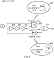
- the edge detector circuit 914 takes the form shown schematically in Figure 5 .
- the input signal provided to the edge detector is routed as one input to both an AND gate circuit 966 and a NOR gate circuit 968.
- a delayed version of the input signal is generated by the series of inverters 960, 962, 964 forming delay circuitry of the edge detector, and that delayed version of the input is provided as the other input to both the AND gate circuitry 966 and the NOR gate circuitry 968. Due to the odd number of inverters in the delay chain, the delayed version of the input signal is also an inverted version of the input signal.
- the NOR gate 968 will produce a short logic one value pulse from the falling edge of the input signal, with again the width of the pulse being dependent on the delay introduced by the delay elements 960, 962, 964.
- the outputs from both the AND gate 966 and the NOR gate 968 can then be logically OR-ed via OR gate circuitry 970 in order to generate the output from the edge detector 914.
- the required width for the pulse will depend on how quickly the NMOS transistor 958 within the current controlled inverter circuit 950 of the delay circuitry of Figure 4 can discharge the capacitance within the capacitor circuitry 940.
- the NMOS transistor 958 will be arranged to be relatively large so as to avoid leakage during the charging phase of the capacitor under high temperature or certain process corners.
- such an approach does limit the speed at which the capacitance can be discharged by the NMOS transistor in the presence of the asserted pulse.
- a delay of at least 300ns is needed. This requires the pulses generated by the edge detector to have a width of 300ns providing enough time for the capacitance to discharge before the control signal then returns to the logic low level, enabling the charging phase of the capacitance to be resumed.
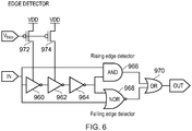
- FIG. 6 One technique that can be used to generate a pulse of the desired width is shown in Figure 6 .
- the circuitry is in essence the same as that shown in Figure 5 , but in addition the two inverters 960, 962 are current controlled inverters, their supply voltage being provided via two PMOS transistors 972, 974 that are arranged to receive the bias voltage generated by the bias voltage generator of Figure 3 . Since that bias voltage causes the PMOS transistors 972, 974 to only partially be turned on, the inverter circuits 960, 962 are driven by a voltage that is less than Vdd. The bias voltage can hence be selected so as to cause the required delay to be introduced by the delay chain 960, 962, 964.
- Figure 7 and 8 illustrate the operation of the edge detector 914 and delay circuitry 912 described earlier, for a situation where regular pulses are generated by the edge detector, and for a situation where regular pulses are not generated, respectively.
- the delay circuitry requires a pulse to be received at least every 10 microseconds.
- this is the case, in that the input signal to the edge detector 914 transitions every 10 microseconds, as shown by the transitions 980, 981, 982. This causes the edge detector to generate the associated pulses 983, 984, 986.
- the capacitance curve 990 each time the pulse is asserted, it causes the capacitance to be discharged, with the capacitance then starting to charge in the intervening period between pulses.
- the capacitance never reaches a voltage level that the inverter circuitry 946 of Figure 4 recognises as a logic one level, and accordingly the output 992 is maintained in the de-asserted state, i.e. the erase signal is not asserted.
- the output 998 from the frequency comparator if provided
- the signal "DLY input” used as the control signal input to the delay circuit 912 is formed directly by the output of the edge detector 914.
- FIG. 9 is a diagram illustrating the frequency comparator circuitry 918 of Figure 2B in accordance with one embodiment.
- the frequency comparator circuitry detects if the input signal provided to the edge detector 914 has the same frequency as the clock signal provided to the frequency comparator, which in one embodiment may be the system clock signal.
- the circuitry comprises a first D-flip flop 1020 and a second D-flip flop 1022.
- the clock signal is provided to the first flip flop 1020 via the delay chain of inverters 1024, 1026, 1028 and the final inverter 1030.
- the second flip flop 1022 receives an inverted version of the clock signal via the delay chain of inverters 1024, 1026, 1028.
- the input provided to the edge detector is also provided as an input to both of the flip flops 1020, 1022.
- the first flip flop 1020 On a rising edge of the clock signal, the first flip flop 1020 outputs the current input value to one input of the exclusive OR (XOR) gate 1032.
- the second flip flop 1022 outputs an inverted version of the input to the other input of the XOR gate 1032.
- the XOR gate 1032 will output a logic one value whilst both of its inputs are different, and will output a logic zero value whenever the outputs are the same.
- the first flip flop 1020 on the rising edge of the clock signal dclk the first flip flop 1020 will output a logic one value.
- the second flip flop On each rising edge of the inverted clock signal clkn the second flip flop will also output a logic one value, since it outputs the inverse of the current input value.
- the frequency comparator will detect that the edge detector input signal is of the same signal frequency as the clock signal, and will accordingly output a logic zero value, causing the AND gate 920 of Figure 2B to output a logic zero value as the control signal, and thereby cause the erase signal to be asserted.
- timer circuitry 904 is placed close to the memory 900 and associated erase circuitry 902, and ideally is provided in the same IP block as the memory device.
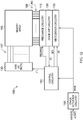
- Figure 12 is a diagram schematically illustrating a logical arrangement of a memory device in accordance with one embodiment.
- the memory device 100 includes a memory array 105 comprising an array of memory cells arranged in a plurality of rows and columns.
- a plurality of word lines 107 are provided through the array in order to allow individual rows of memory cells to be addressed by the word line drivers 130 during write and read operations.
- a plurality of bit lines 109 are provided in association with the columns of memory cells.
- each column is coupled to a pair of bit lines to enable data to be written into an activated memory cell of the column during a write operation, and for data to be read from an activated memory cell of the column during a read operation.
- Precharge circuitry 115 is used to precharge the voltage level on the bit lines under the control of control circuitry 110. Following the precharge operation, a write operation or read operation can be performed. For a write operation, the control circuitry 110 will issue control signals to the word line drivers 130 in order to cause a particular row of memory cells to be activated via the associated word line, and the control circuitry 110 will further cause the write driver circuitry 125 to control the voltages on the relevant bit line pairs, in order to cause the required data values to be written into the memory cells of the activated row.
- control circuitry 110 will issue control signals to the word line drivers 130 in order to cause a particular row of memory cells to be activated via the appropriate word line, and the sense amplifier circuitry 120 will then be used in order to evaluate the voltages on the relevant bit lines, with the sensed read data then being returned to the control circuitry 110.
- control circuitry 110 and write driver circuitry 125 are modified so that in response to an asserted erase signal the control circuitry performs a modified decode operation which causes the word line driver circuitry 130 to assert a word line signal on the word line associated with each row in a predetermined erase region.
- the asserted erase signal also causes the write driver circuitry to control the voltage level on the bit lines for each memory cell in the predetermined erase region in order to cause erase write data to be written in to the memory cells of the predetermined erase region.
- this modified operation occurs independently of the clock signal, and hence will occur even if the clock signal is removed from the memory device.
- erase activation circuitry 150 is configured to monitor certain activity within the system incorporating the memory device in order to detect occurrence of a predetermined condition, and on occurrence of that predetermined condition is arranged to assert the erase signal to both the control circuitry 110 and the write driver circuitry 125.
- the activity that is monitored will depend on the implementation. For example, in a security implementation, the erase activation circuitry 150 may monitor for activity indicative that a processing device has finished utilising secure data stored in the memory array, and when that condition is observed it may then assert the erase signal to cause that sensitive data to be erased from the memory device. Alternatively, the erase activation circuitry may monitor for activities indicative of an attempted hacking operation, and in that instance assert the erase signal.
- the erase activation circuitry employs the delay circuitry, edge detector circuitry, bias generator circuitry, and optionally frequency comparator circuitry, as discussed earlier with reference to figures 1 to 11 .
- the techniques of the described embodiments can be used in a wide variety of memory devices, for example an SRAM memory, a dual port memory, a flash memory, a DRAM memory, a register file, etc.
- the erase activation circuitry 150 may be provided externally to the memory device, or in one embodiment can be provided internally within the memory device.
- Figure 12 is intended to logically illustrate the arrangement of the memory device, it will be appreciated that it is not intended to provide an indication of the structural arrangement.
- the sense amplifier circuitry 120 may actually be embedded within blocks forming the memory array, as may the precharge circuitry 115.
- Figure 13 is a block diagram illustrating in more detail components provided within the control circuitry 110 and the word line driver circuitry 130 of Figure 12 to perform a decoding operation in accordance with one embodiment.
- the decoding operation is split into two separate stages.
- a first stage decoding operation (also commonly referred to as a pre-decode operation) is performed within the control circuitry using the pre-decode circuits 200, 205, 210, 215.
- a further decode stage is performed within the word line drivers of the word line driver circuitry 130, in the embodiment shown these word line drivers 245, 250, 255, 265, 270, 275 being logically grouped into a first group 240 associated with a first bank within the memory array and a second group 260 associated with a second bank in the memory array.
- these word line drivers 245, 250, 255, 265, 270, 275 being logically grouped into a first group 240 associated with a first bank within the memory array and a second group 260 associated with a second bank in the memory array.
- Each of the pre-decode circuits 200, 205, 210 comprises a plurality of intermediate signal generation blocks.
- the circuit 200 is arranged to receive three bits of a received address, along with the inverse values of those address bits, and includes eight intermediate signal generation blocks each configured to receive a predetermined three of the received six values and to generate a corresponding intermediate signal for passing to the routing circuitry 230 (in this embodiment the routing circuitry being considered to be provided within the word line driver circuitry 130).
- Each intermediate signal generation block effectively implements a NAND function, but as will be discussed in more detail later with reference to the remaining figures at least some of those NAND circuits are modified slightly to enable the NAND function to be overridden in the presence of an asserted erase signal.
- the pre-decode circuit 205 is arranged in the same way as the circuit 200, the circuit 205 receiving a further three address bits and the inverted versions of those address bits, and generating a further eight intermediate signals for routing to the routing circuitry 230. Again, one or more of the NAND circuits within the pre-decode circuitry 205 may be modified in order to override the NAND functionality in the presence of an asserted erase signal.
- the pre-decode circuitry 210 consists of four two input NAND circuits, and the pre-decode circuitry 210 receives a further two address bits and the inverted versions of those address bits.
- the outputs from the pre-decode circuit 210 are not provided directly to the routing circuitry, but instead are provided as a sequence of bank select signals to the clock circuitry 215.
- each of the two banks A and B are actually addressable in two halves, referred to as top and bottom halves, and accordingly the four outputs from the pre-decode circuitry 210 are used to identify which of those four possible regions is to be addressed.
- the clock circuitry is provided with a clock override function 220 which, on receipt of an asserted erase signal, will override such functionality in respect of at least one of the four sections, and will instead issue an asserted signal over the relevant clock path irrespective of the input received from the pre-decode circuit 210, and irrespective of the state of the global clock signal.
- each intermediate signal generation block may comprise a NAND circuit 300 and two inverter circuits 305, 310.
- each intermediate signal generation block may comprise a NAND circuit 300 and two inverter circuits 305, 310.
- the NAND gate issue a logic zero value, and accordingly only in that particular situation will a logic zero value ultimately be output from the inverter 310.
- only one intermediate signal generation block within the pre-decoder circuit 200 and one intermediate signal generation block within the pre-decoder circuit 205 will receive three logic one inputs, and accordingly only those two intermediate signal generation blocks will output a logic zero value.
- the routing circuitry 230 routes different pairs of the intermediate signals to each of the various word line driver circuits 245, 250, 255, 265, 270, 275. Due to the two sets of eight intermediate signals generated by the pre-decode circuits 200, 205, this gives rise to 64 possible combinations, and hence typically four of the 256 word line drivers will receive a pair of inputs that are both at a logic zero value.
- the pre-decode circuitry 210 will also be arranged such that only one of its outputs will be at a logic zero value, and accordingly via the clock circuitry, only one of the four clock signal paths will be asserted. Accordingly, only one of the word line driver circuits will receive both two logic zero inputs from the routing circuitry, and an asserted clock signal, and accordingly during normal operation only one of the word line signals will be asserted.
- the operation of the clock circuitry 215 is shown in Figure 14 by the components 320, 325.
- the clock circuitry will replicate the components 320, 325 for each of the four inputs from the pre-decode circuitry 210.
- only one of the output signals from circuitry 210 will be at a logic zero value.
- Bank select signals are determined from the inverse of those output signals and hence only one bank select signal will be at a logic one value. Accordingly, on a rising edge of the global clock signal, the relevant NAND gate 320 will receive two logic one input values and will hence output a logic zero value, thus causing the inverter 325 to output a logic one value to the NAND gate 330.
- Each of the word line driver circuits 245, 250, 255, 265, 270, 275 includes the components 315, 330, 335.
- four word line driver circuits will receive the same combination of two intermediate signals from the routing circuitry, and accordingly the NOR gate 315 can be shared between those four drivers. As will be appreciated, only when the two input signals to the NOR gate 315 are both at a logic zero value will a logic one value be output as the row select signal from that NOR gate.
- the intermediate signal generation blocks within the pre-decode circuits 200 and 205 are modified as shown in Figure 15 .
- the standard NAND gate 300 is replaced with an AND gate 340 and a NOR gate 345.
- the erase signal is asserted this causes the output of the NOR gate 345 to change to a logic zero value irrespective of the three address inputs to AND gate 340, which in turn causes a logic zero value to be output from the inverter 310.
- this causes multiple of the intermediate signals to be issued at a logic zero value, and this in turn means that multiple of the NOR gates 315 within the word line driver circuits can be arranged to receive two logic zero values. This hence enables multiple word lines to be activated at the same time.
- Similar circuitry will also be incorporated within at least one of the clock circuits within the clock circuitry 215. Accordingly, the NAND gate function 320 of Figure 14 is replaced by an AND gate 350 and NOR gate 355. When the erase signal is unasserted, this hence does not affect the operation of the clock circuitry, but when the erase signal is asserted, this effectively overrides the global clock signal, and causes a logic zero value to be output from the NOR gate 355, which in turn causes a logic one value to be output from the inverter 325. For the corresponding section of the memory array (i.e. the top part or the bottom part of bank A or the top part or the bottom part of bank B) this will mean that all of the word line drivers will be primed to assert their word line signal in the event that their associated NOR gate 315 receives two logic zero values.
- this approach enables multiple word lines to be asserted at the same time, and in a clock independent manner. This hence provides a very efficient mechanism for overwriting data within a predetermined erase region of the memory array.
- the exact configuration of the predetermined erase region can be determined by deciding which of the various intermediate signal generation blocks within the pre-decoders 200, 205 and which of the clock circuits within the clock circuitry 215 to modify in accordance with the circuitry of Figure 15 .
- Figure 16 shows an efficient mechanism for modifying a NAND gate structure to produce the structure 340, 345 or 350, 355 of Figure 15 .
- the basic NAND circuit comprises three PMOS transistors 360, 362, 364 in parallel, coupled to three NMOS transistors 366, 368, 370 in series. Each PMOS transistor receives a corresponding one of the three address inputs, as do each of the three NMOS transistors.
- an NMOS transistor 385 is coupled between the output node 375 over which the intermediate signal is output, and a ground potential, with that NMOS transistor being driven by the erase signal.
- a PMOS transistor 380 is coupled between the power supply and the parallel configuration of PMOS transistors 360, 362, 364, this PMOS transistor also being driven by the erase signal.
- the PMOS transistor 380 is turned on and the NMOS transistor 385 is turned off, and accordingly the circuitry operates as a standard NAND gate.
- the PMOS transistor 380 turns off, decoupling the NAND gate structure from the power supply.
- the NMOS transistor 385 turns on, discharging the output node 375 to ground (i.e. a logic zero value).
- the PMOS transistor 380 is shared amongst all of the intermediate signal generation blocks within a particular pre-decode circuit 200, 205 whose function is to be modified by the erase signal. Hence, if all eight of the intermediate signal generation blocks within a particular pre-decode circuit 200, 205 are to be modified, then it will be seen that a total of nine additional transistors (eight NMOS transistors and one PMOS transistor) needs to be added to the pre-decode circuitry. This provides a particularly small increase in gate count, which makes the presence of this modification circuitry very difficult to detect, hence further improving security.
- Figure 17 illustrates how the write driver circuitry 125 may be modified to control the voltages on the bit lines in the presence of an asserted erase signal.
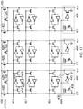
- the memory array 105 comprises an array of 6T SRAM memory cells, each 6T SRAM memory cell comprising a pair of inverters 400, 405, and two NMOS transistors 410, 415.
- one of the word line signals would be asserted, turning on the NMOS transistors 410, 415 for each memory cell in the row associated with that asserted word line signal.
- This hence couples the pair of inverters 400, 405 to the bit lines, and enables the data value to be written into each of the addressed memory cells dependent on the value present on each of the bit lines.
- precharge circuitry 420 is used to precharge each of the bit lines to a logic one voltage level prior to a write operation.
- the PMOS transistors 425 are also considered to form part of the precharge circuitry, and ensure that both bit lines are coupled together during the precharge operation, thereby ensuring that exactly the same voltage is present on the bit lines of each bit line pair at the end of the precharge operation.
- the precharge signal is de-asserted to a logic one level, hence turning the precharge transistors 420, 425 off.
- the write driver circuitry 125 will pull the voltage on one bit line of each bit line pair to a logic zero value, in order to cause the required data value to be written into the addressed memory cells.
- the write driver circuitry also includes some additional components to control the voltages on each bit line pair in response to an asserted erase signal.
- the inverted erase signal provided over path 430 will be at a logic zero value. This will cause the PMOS transistor 435 in each circuit block 450 to turn on, thereby retaining the left hand side bit line at the logic one value.
- the inverter 440 this will cause the NMOS transistor 445 to turn on, hence pulling the voltage on the right hand side bit line of each bit line pair down to a logic zero value.
- Figure 17 is merely provided as one example of how the write driver circuitry can be modified to respond to the asserted erase signal.
- every block 450 is configured in the same way, nor indeed is there any requirement that the two bit lines in each bit line pair are pulled in opposite directions.
- the blocks 450 can be configured to pull both bit lines in each bit line pair to the logic zero value, which will effectively mean that random data is stored in each of the memory cells connected to an asserted word line. However, this is still sufficient to ensure that whatever data was previously stored in those memory cells has now been overwritten and can no longer be accessed, hence preventing a hacker from taking advantage of the earlier described remanence effects.
- the write driver circuitry 125 can merely be arranged to store into each row receiving an asserted word line signal the data values currently present on its input pins.
- the above described embodiments provide a very efficient and effective mechanism for overwriting multiple rows of the memory array within the predetermined erase region, they can give rise to a significant in rush current being drawn by the word line driver circuits.
- the final inverter circuits 335 provided in each word line driver circuit are typically quite large, and if a large number of those are turned on simultaneously, this will give rise to a large, and easily detectable, in rush current being drawn by the word line driver circuitry 130.
- the transition of each word line from the unasserted to the asserted state will occur more slowly than would be the case when a single word line is asserted. This means that it will take longer for the addressed memory cells to be written to, and this can increase the crowbar current, and in turn require the sizing of the write driver components within the blocks 450 to be increased.
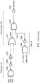
- Figure 18A illustrates a staggered delay mechanism that can be used to alleviate these issues.
- the timing of the propagation of the asserted erase signal to the NOR gates 345 is staggered, such that the timing of the transition of the intermediate signals to a logic zero value is staggered. This in turn will stagger the timing at which the word lines are asserted, thereby reducing the in rush current.
- the timing of the transmission of that erase signal to those intermediate signal generation blocks is staggered.
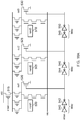
- each of the basic NAND gate circuits 500, 505, 510 is modified as discussed earlier with reference to Figure 16 by the addition of a separate NMOS transistor 520, 525, 530 for each signal generation block, but with the signal generation blocks sharing the PMOS transistor 515.
- the erase signal is provided immediately to the PMOS transistor, but is delayed before being provided to the NMOS transistors.
- each NMOS transistor 520, 525, 530 receives the erase signal at a different time. Hence, output 1 will transition to the logic zero value before output 2, and output 2 will transition to the logic zero value before output 3.
- an associated delay element 570, 574, 578, 582 ensures that the propagation of the erase signal is delay differentially before being supplied to each of those blocks. Due to the earlier described operation of the pre-decode circuitry in a normal mode of operation (i.e. where the erase signal is de-asserted), it will always be the case that the output from one of the NAND circuits is at a logic zero value, with the remaining outputs being at a logic one value. However, which one is outputting a logic zero value will depend entirely on the last provided input to the pre-decode circuitry 200.
- NAND circuit 6 576 will output a logic zero value but all of the other NAND circuits within the pre-decode circuitry 200 will output a logic one value. Combined with the eight logic zero values output from the pre-decode circuitry 205, this will mean that 32 word lines (i.e. 1/8 th of the total word lines) will be activated at time 0 for the configuration shown in Figure 13 .
- NAND circuit 7 572 has now received the asserted erase signal, and accordingly has transitioned its output to a logic zero value. As a result, another 32 word lines will be selected.
- NAND circuit 6 576 receives the asserted erase signal, but since its output was already at a logic zero value, the same 32 word lines will be addressed at that point.
- NAND circuit 5 580 will also receive the asserted word line signal, causing a further 32 word lines to be asserted. This process will continue until all of the NAND circuits within the pre-decoder circuitry 200 have received the asserted word line signal, and accordingly have transitioned their intermediate output to a logic zero value, at which time all of the word lines will be asserted.
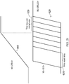
- Such an approach means that the forced write operation used to overwrite the values in the memory array is performed in a staggered manner. This is illustrated schematically in Figure 19 .
- the transition 560 without the staggered approach discussed in Figures 18A and 18B , all 256 word lines will be asserted at the same time, but the slope will be relatively shallow since it will take significantly longer to drive the word lines to the logic one value. There will also be a significantly large in rush current.
- the word lines transition in blocks of 32, and due to the reduced loading the transition to the asserted value occurs more quickly. This is shown schematically by the series of transitions 565 shown in Figure 19 , and over the course of eight stages all of the word lines will transition to the logic one value.
- the delay elements are illustrated schematically in Figure 18A by a series of inverters, it will be appreciated that the delay mechanisms can take a variety of forms, for example an inverter delay or a resistor/capacitor based delay, or a mixture of those delay types.
- the steeper word line transitions that occur when using the staggered approach also significantly improve the writeability of the addressed bit cells, ensuring that they flip state more cleanly, without drawing too much cross current. This limits the total power consumption, and also enables the sizing of the components within blocks 450 of Figure 17 to be reduced.
- the granularity of the staggering of the propagation of the erase signal can be varied as desired.
- the more staggering steps introduced the smaller the number of word lines asserted at each point in time, and the more smoothly the in rush current will be spread out.
- the more staggering steps introduced the longer the delay that will be added.
- this write assist mechanism introduces an additional delay 630, due to the increased initial propagation delay 625 of the asserted erase signal.
- the general profile 620 of the asserted word lines is similar to that as discussed earlier with reference to Figure 19 .
- Figure 22 schematically illustrates how a memory instance including hacking prevention mechanisms in accordance with the above described embodiments may be created from a memory compiler 700 with reference to a memory architecture 710.
- the memory architecture 710 specifies a definition of circuit elements and data defining rules for combining those circuit elements in order to create a memory instance.
- Particular requirements for the memory instance are entered into the memory compiler 700 as input parameters via a graphical user interface (GUI).
- GUI graphical user interface
- input parameters can specify various aspects of the desired memory instance, for example defining the size of the memory array, the multiplexing arrangements of the memory array, selection of various optional features such as power gating features, built-in-self-test (BIST) modes to be supported, etc.
- Input parameters entered via the GUI can also be used to select or deselect the various hacking prevention mechanisms described herein, such as the un-interruptible fast memory erase circuitry 902, the if-not timer circuitry 904, and the pulse intrusion circuitry 906 of Figure 1 .
- the memory compiler 700 then generates the required memory instance based on the input parameters and the memory architecture 710.
- the memory compiler includes, dependent on parameters entered via the GUI, additional components to implement the hacking prevention mechanisms of the above described embodiments, in the manner described with reference to the earlier figures.
- FIG 23 schematically illustrates a general purpose computer 800 of the type that may be used to implement the above described memory compilation operation in order to generate a memory instance.
- the general purpose computer 800 includes a central processing unit 802, a random access memory 804, a read only memory 806, a network interface card 808, a hard disk drive 810, a display driver 812 and monitor 814 and a user input/output circuit 816 with a keyboard 818 and mouse 820 all connected via a common bus 822.
- the central processing unit 802 will execute computer program instructions that may be stored in one or more of the random access memory 804, the read only memory 806 and the hard disk drive 810 or dynamically downloaded via the network interface card 808.
- the results of the processing performed may be displayed to a user via the display driver 812 and the monitor 814.
- User inputs for controlling the operation of the general purpose computer 800 may be received via the user input output circuit 816 from the keyboard 818 or the mouse 820 (and hence for example the input parameters used to determine certain properties of the required memory instance can be entered via this mechanism).
- the computer program could be written in a variety of different computer languages.
- the computer program may be stored and distributed on a recording medium or dynamically downloaded to the general purpose computer 800.
- the general purpose computer 800 can perform the above described memory compiler operation and can be considered to form an apparatus for performing the above described memory compiler operation.
- the architecture of the general purpose computer 800 could vary considerably and Figure 23 is only one example.
Landscapes
- Engineering & Computer Science (AREA)
- Computer Security & Cryptography (AREA)
- Microelectronics & Electronic Packaging (AREA)
- Read Only Memory (AREA)
- Storage Device Security (AREA)
Claims (14)
- Vorrichtung, die Folgendes umfasst:eine Speichervorrichtung (900), die eine Anordnung von Speicherzellen umfasst und dafür konfiguriert ist, auf der Basis eines Taktsignals zu arbeiten;eine Löschschaltung (902), die dafür ausgelegt ist, in Reaktion auf den Empfang eines Löschsignals in einem aufgedrückten Zustand einen erzwungenen Schreibvorgang unabhängig von dem Taktsignal in Bezug auf jede Speicherzelle innerhalb einer zuvor festgelegten Löschregion der Anordnung auszuführen; undeine Löschsignalgenerierungsschaltung (912), die dafür konfiguriert ist, ein Steuerungssignal zu empfangen und das Löschsignal in einem nicht-aufgedrückten Zustand zu halten, sofern das Steuerungssignal die Form eines Impulssignals annimmt, das mindestens eine zuvor festgelegte Mindestfrequenz zwischen Impulsen;wobei die Löschsignalgenerierungsschaltung dafür konfiguriert ist, das Löschsignal in dem aufgedrückten Zustand auszugeben, falls das Steuerungssignal beendet wird oder falls das Steuerungssignal nicht die Form des Impulssignals annimmt;wobei:die Löschsignalgenerierungsschaltung eine Kondensatorschaltung (940) und eine Ausgabeschaltung (945) umfasst, die dafür konfiguriert ist, das Löschsignal in Abhängigkeit von einer Ausgabe von der Kondensatorschaltung zu generieren;die Kondensatorschaltung dafür konfiguriert ist, in Abhängigkeit von dem Steuerungssignal zwischen einem Ladevorgang und einem Entladevorgang umzuschalten;falls das Steuerungssignal beendet wird oder falls das Steuerungssignal nicht die Form des Impulssignals annimmt, die Ausgabe von der Kondensatorschaltung dafür konfiguriert ist, einen zuvor festgelegten Aktivierungsspannungspegel zu erreichen, wodurch die Ausgabeschaltung veranlasst wird, das Löschsignal in dem aufgedrückten Zustand zu generieren; undfalls das Steuerungssignal die Form des Impulssignals annimmt, die Ausgabe von der Kondensatorschaltung dafür konfiguriert ist, nicht den zuvor festgelegten Aktivierungsspannungspegel zu erreichen, wodurch veranlasst wird, dass das Löschsignal in dem nicht-aufgedrückten Zustand gehalten wird.
- Vorrichtung nach Anspruch 1, wobei die Kondensatorschaltung (940) dafür konfiguriert ist, den Ladevorgang immer dann auszuführen, wenn das Steuerungssignal keinen Impuls enthält, und für die Dauer jedes Impulses in dem Steuerungssignal zu dem Entladevorgang umzuschalten.
- Vorrichtung nach Anspruch 1 oder Anspruch 2, wobei die Löschsignalgenerierungsschaltung (912) einen stromgesteuerten Inverterschaltkreis (950) umfasst, der dafür konfiguriert ist, in Abhängigkeit von dem Steuerungssignal ein Eingangssignal in die Kondensatorschaltung (940) einzuspeisen.
- Vorrichtung nach Anspruch 3, die des Weiteren eine Vorspannungsgenerierungsschaltung (916) umfasst, die dafür konfiguriert ist, eine Vorspannung zu generieren, die in mindestens eine Komponente innerhalb der stromgesteuerten Inverterschaltung (950) eingespeist wird, um eine Rate zu steuern, mit der sich der Spannungspegel der Ausgabe der Kondensatorschaltung (940) während des Ladevorgangs und/oder des Entladevorgangs ändert.
- Vorrichtung nach Anspruch 4, wobei:die Kondensatorschaltung (940) dafür konfiguriert ist, den Ladevorgang immer dann auszuführen, wenn das Steuerungssignal keinen Impuls enthält, und für die Dauer jedes Impulses in dem Steuerungssignal zu dem Entladevorgang umzuschalten; unddie stromgesteuerte Inverterschaltung (950) dafür konfiguriert ist, die durch die Vorspannungsgenerierungsschaltung generierte Vorspannung zu verwenden, um die Rate zu steuern, mit der sich der Spannungspegel der Ausgabe der Kondensatorschaltung während des Ladevorgangs ändert.
- Vorrichtung nach einem der vorangehenden Ansprüche, die des Weiteren eine Steuerungssignalgenerierungsschaltung umfasst, die dafür konfiguriert ist, das in die Löschsignalgenerierungsschaltung (912) eingespeiste Steuerungssignal zu generieren, wobei die Steuerungssignalgenerierungsschaltung eine Flankendetektorschaltung (914) umfasst, die dafür konfiguriert ist, jedes Mal ein Eingangssignal zu empfangen und einen Impuls innerhalb des Steuerungssignals zu generieren, wenn das Eingangssignal seinen Zustand zwischen einem ersten und einem zweiten Spannungspegel ändert.
- Vorrichtung nach Anspruch 6, wobei die Flankendetektorschaltung (914) eine Verzögerungsschaltung (960, 962, 964) umfasst, die dafür konfiguriert ist, ein verzögertes Eingangssignal zu generieren, und eine Vergleichsschaltung (966, 968, 970) umfasst, die dafür konfiguriert ist, jeden der Impulse in Abhängigkeit von einem Vergleich zwischen dem Eingangssignal und dem verzögerten Eingangssignal zu generieren.
- Vorrichtung nach Anspruch 7, wobei eine durch die Verzögerungsschaltung (960, 962, 964) herbeigeführte Verzögerung eine Breite jedes durch die Flankendetektorschaltung (914) generierten Impulses bestimmt.
- Vorrichtung nach Anspruch 8, die des Weiteren eine Vorspannungsgenerierungsschaltung (916) umfasst, die dafür konfiguriert ist, eine Vorspannung zu generieren, die in mindestens eine Komponente innerhalb der Verzögerungsschaltung eingespeist wird, um die durch die Verzögerungsschaltung herbeigeführte Verzögerung zu steuern.
- Vorrichtung nach einem der Ansprüche 6 bis 9, wobei die Steuerungssignalgenerierungsschaltung des Weiteren eine Impulsaußerkraftsetzungsschaltung (918) umfasst, die dafür konfiguriert ist, bei Detektion mindestens einer zuvor festgelegten Bedingung unabhängig von der Ausgabe der Flankendetektorschaltung (914) zu verhindern, dass das Steuerungssignal die Form des Impulssignals annimmt, um dadurch die Löschsignalgenerierungsschaltung zu veranlassen, das Löschsignal in dem aufgedrückten Zustand auszugeben.
- Vorrichtung nach einem der vorangehenden Ansprüche, wobei:die Anordnung von Speicherzellen als mehrere Reihen und Spalten ausgebildet ist, wobei jede Reihe von Speicherzellen mit einer zugehörigen Wortleitung (107) gekoppelt ist und jede Spalte von Speicherzellen mit einer zugehörigen mindestens einen Bitleitung (109) gekoppelt ist;wobei die Vorrichtung des Weiteren Folgendes umfasst:eine Decoderschaltung (110), die dafür konfiguriert ist, in Reaktion auf einen Schreibvorgang eine mit dem Schreibvorgang verknüpfte Adressenanzeige zu decodieren, um die Reihe zu bestimmen, die adressierte Speicherzellen für den Schreibvorgang enthält, und in Abhängigkeit von dem Taktsignal ein aufgedrücktes Wortleitungssignal auf der zugehörigen Wortleitung für die bestimmt Reihe auszugeben; undeine Schreibschaltung (125), die dafür konfiguriert ist, in Reaktion auf den Schreibvorgang einen Spannungspegel der zugehörigen mindestens einen Bitleitung für jede der adressierten Speicherzellen zu steuern, um zu veranlassen, dass Schreibdaten in die adressierten Speicherzellen geschrieben werden;die Löschschaltung (902) die Decoderschaltung und die Schreibschaltung umfasst, wobei die Decoderschaltung dafür konfiguriert ist, in Reaktion auf das aufgedrückte Löschsignal unabhängig von dem Taktsignal das aufgedrückte Wortleitungssignal auf der Wortleitung auszugeben, die mit jeder Reihe in der zuvor festgelegten Löschregion verknüpft ist; unddie Schreibschaltung dafür konfiguriert ist, in Reaktion auf den aufgedrückten Löschsignal den Spannungspegel der zugehörigen mindestens einen Bitleitung für jede Speicherzelle in der zuvor festgelegten Löschregion zu steuern, um zu veranlassen, dass Löschschreibdaten in die Speicherzellen der zuvor festgelegten Löschregion geschrieben werden.
- Vorrichtung nach einem der vorangehenden Ansprüche, wobei die zuvor festgelegte Löschregion eines von Folgendem umfasst:die gesamte Anordnung;eine oder mehrere Reihen der Anordnung; undeine oder mehrere Spalten der Anordnung.
- Verfahren zum Betreiben einer Vorrichtung, um Daten in einer Speichervorrichtung (900) zu löschen, die eine Anordnung von Speicherzellen umfasst und die dafür konfiguriert ist, auf der Basis eines Taktsignals zu arbeiten, wobei das Verfahren Folgendes umfasst:in Reaktion auf ein Löschsignal in einem aufgedrückten Zustand, Ausführen eines erzwungenen Schreibvorgangs unabhängig von dem Taktsignal in Bezug auf jede Speicherzelle innerhalb einer zuvor festgelegten Löschregion der Anordnung;Aufrechthalten des Löschsignals in einem nicht-aufgedrückten Zustand, sofern ein Steuerungssignal die Form eines Impulssignals annimmt, das mindestens eine zuvor festgelegte Mindestfrequenz zwischen Impulsen aufweist; undAusgeben des Löschsignals in dem aufgedrückten Zustand, falls das Steuerungssignal beendet wird oder falls das Steuerungssignal nicht die Form des Impulssignals annimmt; wobei:die Schritte des Aufrechthaltens und des Ausgebens das Generieren des Löschsignals in Abhängigkeit von einer Ausgabe von der Kondensatorschaltung (940) umfassen, die dafür konfiguriert ist, zwischen einem Ladevorgang und einem Entladevorgang in Abhängigkeit von dem Steuerungssignal umzuschalten, dergestalt, dass, falls das Steuerungssignal beendet wird oder falls das Steuerungssignal nicht die Form des Impulssignals annimmt, die Ausgabe von der Kondensatorschaltung dafür konfiguriert ist, einen zuvor festgelegten Aktivierungsspannungspegel zu erreichen, wodurch veranlasst wird, dass das Löschsignal in dem aufgedrückten Zustand generiert wird; undfalls das Steuerungssignal die Form des Impulssignals annimmt, die Ausgabe von der Kondensatorschaltung dafür konfiguriert ist, den zuvor festgelegten Aktivierungsspannungspegel nicht zu erreichen, wodurch veranlasst wird, dass das Löschsignal im nicht-aufgedrückten Zustand gehalten wird.
- Computerprogramm-Speichermedium, das ein Speicherkompilierer-Computerprogramm (700) speichert, um einen Computer zu veranlassen, eine Instanz einer Speichervorrichtung anhand einer Speicherarchitektur (710) zu generieren, die mit dem Speicherkompilierer-Computerprogramm verknüpft ist, wobei die Speicherarchitektur eine Definition von Schaltkreiselementen und Datendefinierungsregeln, um diese mit den Schaltkreiselementen zu kombinieren, spezifiziert, dergestalt, dass die generierte Instanz eine Speichervorrichtung spezifiziert, die durch die Vorrichtung nach einem der Ansprüche 1 bis 12 gebildet ist.
Applications Claiming Priority (2)
| Application Number | Priority Date | Filing Date | Title |
|---|---|---|---|
| US13/915,918 US8885429B1 (en) | 2013-06-12 | 2013-06-12 | Memory device and a method for erasing data stored in the memory device |
| US13/943,029 US9036427B2 (en) | 2013-06-12 | 2013-07-16 | Apparatus and a method for erasing data stored in a memory device |
Publications (3)
| Publication Number | Publication Date |
|---|---|
| EP2814034A2 EP2814034A2 (de) | 2014-12-17 |
| EP2814034A3 EP2814034A3 (de) | 2014-12-24 |
| EP2814034B1 true EP2814034B1 (de) | 2018-11-28 |
Family
ID=50942033
Family Applications (1)
| Application Number | Title | Priority Date | Filing Date |
|---|---|---|---|
| EP14170409.8A Active EP2814034B1 (de) | 2013-06-12 | 2014-05-28 | Vorrichtung und Verfahren zum Löschen von in einer Speichervorrichtung gespeicherten Daten |
Country Status (2)
| Country | Link |
|---|---|
| US (1) | US9036427B2 (de) |
| EP (1) | EP2814034B1 (de) |
Families Citing this family (10)
| Publication number | Priority date | Publication date | Assignee | Title |
|---|---|---|---|---|
| US10186310B2 (en) * | 2015-10-31 | 2019-01-22 | Goran Krilic | DIMM DRAM memory chips quick optical data erasure after power cycling |
| WO2017138775A1 (ko) * | 2016-02-12 | 2017-08-17 | 한양대학교 산학협력단 | 메모리 장치 및 그 동작 방법 |
| US10403384B2 (en) | 2016-06-22 | 2019-09-03 | Darryl G. Walker | Testing a semiconductor device including a voltage detection circuit and temperature detection circuit that can be used to generate read assist and/or write assist in an SRAM circuit portion and method therefor |
| US9940999B2 (en) | 2016-06-22 | 2018-04-10 | Darryl G. Walker | Semiconductor devices, circuits and methods for read and/or write assist of an SRAM circuit portion based on voltage detection and/or temperature detection circuits |
| US11443820B2 (en) * | 2018-01-23 | 2022-09-13 | Microchip Technology Incorporated | Memory device, memory address decoder, system, and related method for memory attack detection |
| CN108417240B (zh) * | 2018-03-05 | 2019-10-01 | 长鑫存储技术有限公司 | 存储器的控制电路、存储器及其控制方法 |
| US11487464B2 (en) * | 2019-07-03 | 2022-11-01 | Micron Technology, Inc. | Neural network memory |
| US11789647B2 (en) * | 2019-12-20 | 2023-10-17 | Micron Technology, Inc. | Address verification for a memory device |
| US11972793B2 (en) | 2021-09-15 | 2024-04-30 | Mavagail Technology, LLC | Integrated circuit device including an SRAM portion having end power select circuits |
| FR3143947B1 (fr) * | 2022-12-20 | 2025-10-03 | Commissariat Energie Atomique | Mémoire SRAM à initialisation déterministe aléatoire |
Citations (1)
| Publication number | Priority date | Publication date | Assignee | Title |
|---|---|---|---|---|
| US20060087882A1 (en) * | 2004-10-26 | 2006-04-27 | Tom Kinsley | Data retention kill function |
Family Cites Families (10)
| Publication number | Priority date | Publication date | Assignee | Title |
|---|---|---|---|---|
| US5668760A (en) * | 1996-04-23 | 1997-09-16 | Intel Corporation | Nonvolatile memory with a write protection circuit |
| AUPO799197A0 (en) | 1997-07-15 | 1997-08-07 | Silverbrook Research Pty Ltd | Image processing method and apparatus (ART01) |
| JP2000048565A (ja) | 1998-07-29 | 2000-02-18 | Mitsubishi Electric Corp | 同期型半導体記憶装置 |
| TW446949B (en) | 1999-10-06 | 2001-07-21 | Winbond Electronics Corp | Apparatus and method for protecting rewritable nonvolatile memory from data damage |
| DE60312704T2 (de) | 2003-12-12 | 2007-12-06 | Banksys S.A. | Elektronische Datenverarbeitungseinrichtung |
| GB2451592B (en) | 2004-05-12 | 2009-11-25 | Spansion Llc | Erasing memory using sector based activation information |
| JP2006031821A (ja) | 2004-07-16 | 2006-02-02 | Sharp Corp | 不揮発性半導体記憶装置 |
| EP1672647B1 (de) * | 2004-12-15 | 2011-04-27 | STMicroelectronics Srl | Ein nichtflüchtiger Speicher mit Unterstützung von hochparallelem Test auf Waferebene |
| WO2008150939A1 (en) | 2007-05-30 | 2008-12-11 | Summit Design Solutions, Inc. | Method and device for protecting information contained in an integrated circuit |
| US7570532B1 (en) | 2007-07-26 | 2009-08-04 | Zilog, Inc. | Overwriting memory cells using low instantaneous current |
-
2013
- 2013-07-16 US US13/943,029 patent/US9036427B2/en active Active
-
2014
- 2014-05-28 EP EP14170409.8A patent/EP2814034B1/de active Active
Patent Citations (1)
| Publication number | Priority date | Publication date | Assignee | Title |
|---|---|---|---|---|
| US20060087882A1 (en) * | 2004-10-26 | 2006-04-27 | Tom Kinsley | Data retention kill function |
Also Published As
| Publication number | Publication date |
|---|---|
| EP2814034A2 (de) | 2014-12-17 |
| US20140369139A1 (en) | 2014-12-18 |
| EP2814034A3 (de) | 2014-12-24 |
| US9036427B2 (en) | 2015-05-19 |
Similar Documents
| Publication | Publication Date | Title |
|---|---|---|
| US9036427B2 (en) | Apparatus and a method for erasing data stored in a memory device | |
| US8885429B1 (en) | Memory device and a method for erasing data stored in the memory device | |
| US9147451B2 (en) | Memory device and method of controlling leakage current within such a memory device | |
| KR102379369B1 (ko) | 메모리의 리프레시 결여 검출을 위한 장치 및 방법 | |
| US8988954B2 (en) | Memory device and method of performing a read operation within such a memory device | |
| KR101110994B1 (ko) | 에러 동작으로부터 집적 회로를 보호하는 방법 및 장치 | |
| US20080232151A1 (en) | System and method to control one time programmable memory | |
| US9696772B2 (en) | Controlling access to a memory | |
| US9064559B2 (en) | Memory device and method of performing access operations within such a memory device | |
| KR100680975B1 (ko) | 파워다운 모드 제어 회로 | |
| US7295481B2 (en) | Power saving by disabling cyclic bitline precharge | |
| EP3405954B1 (de) | Statischer direktzugriffspeicher mit verbesserter schreibzeit und reduzierter schreibleistung | |
| US7339842B1 (en) | Timing control for sense amplifiers in a memory circuit | |
| US11586778B2 (en) | Secured memory | |
| US9373377B2 (en) | Apparatuses, integrated circuits, and methods for testmode security systems | |
| US8395963B2 (en) | Data security for dynamic random access memory at power-up | |
| KR20160015185A (ko) | 메모리 장치에서의 액세스 억제 | |
| US8082401B2 (en) | Self-timing for a multi-ported memory system | |
| US11043248B2 (en) | Circuit for detection of predominant data in a memory cell | |
| GB2520291B (en) | A memory device and method of performing a read operation within such a memory device | |
| Erbagci et al. | A 32kb secure cache memory with dynamic replacement mapping in 65nm bulk CMOS | |
| Zhang et al. | Using Canary Cell to Detect and Prevent Rowhammer Attack | |
| Xiao et al. | A physically-secure write scheme of Multi-time Programmable RRAM for critical information storage | |
| CN114860626A (zh) | 一种具有老化检测和自毁功能的atd电路模块 | |
| Lee et al. | Minimizing Power Dissipation during Write Operation to Register Files |
Legal Events
| Date | Code | Title | Description |
|---|---|---|---|
| PUAL | Search report despatched |
Free format text: ORIGINAL CODE: 0009013 |
|
| 17P | Request for examination filed |
Effective date: 20140528 |
|
| AK | Designated contracting states |
Kind code of ref document: A2 Designated state(s): AL AT BE BG CH CY CZ DE DK EE ES FI FR GB GR HR HU IE IS IT LI LT LU LV MC MK MT NL NO PL PT RO RS SE SI SK SM TR |
|
| AX | Request for extension of the european patent |
Extension state: BA ME |
|
| PUAI | Public reference made under article 153(3) epc to a published international application that has entered the european phase |
Free format text: ORIGINAL CODE: 0009012 |
|
| AK | Designated contracting states |
Kind code of ref document: A3 Designated state(s): AL AT BE BG CH CY CZ DE DK EE ES FI FR GB GR HR HU IE IS IT LI LT LU LV MC MK MT NL NO PL PT RO RS SE SI SK SM TR |
|
| AX | Request for extension of the european patent |
Extension state: BA ME |
|
| RIC1 | Information provided on ipc code assigned before grant |
Ipc: G11C 8/20 20060101ALI20141117BHEP Ipc: G11C 7/24 20060101AFI20141117BHEP Ipc: G11C 16/22 20060101ALI20141117BHEP |
|
| R17P | Request for examination filed (corrected) |
Effective date: 20150624 |
|
| RBV | Designated contracting states (corrected) |
Designated state(s): AL AT BE BG CH CY CZ DE DK EE ES FI FR GB GR HR HU IE IS IT LI LT LU LV MC MK MT NL NO PL PT RO RS SE SI SK SM TR |
|
| STAA | Information on the status of an ep patent application or granted ep patent |
Free format text: STATUS: EXAMINATION IS IN PROGRESS |
|
| 17Q | First examination report despatched |
Effective date: 20161125 |
|
| GRAP | Despatch of communication of intention to grant a patent |
Free format text: ORIGINAL CODE: EPIDOSNIGR1 |
|
| STAA | Information on the status of an ep patent application or granted ep patent |
Free format text: STATUS: GRANT OF PATENT IS INTENDED |
|
| INTG | Intention to grant announced |
Effective date: 20180608 |
|
| RIC1 | Information provided on ipc code assigned before grant |
Ipc: G11C 7/22 20060101ALN20180525BHEP Ipc: G11C 16/22 20060101ALI20180525BHEP Ipc: G11C 7/24 20060101AFI20180525BHEP Ipc: G11C 8/20 20060101ALI20180525BHEP |
|
| RIN1 | Information on inventor provided before grant (corrected) |
Inventor name: AGHETTI, BASTIEN JEAN CLAUDE Inventor name: ALAOUI, ALI Inventor name: LEMARCHAND, PIERRE Inventor name: VAN WINKELHOFF, NICOLAAS KLARINUS JOHANNES |
|
| GRAJ | Information related to disapproval of communication of intention to grant by the applicant or resumption of examination proceedings by the epo deleted |
Free format text: ORIGINAL CODE: EPIDOSDIGR1 |
|
| STAA | Information on the status of an ep patent application or granted ep patent |
Free format text: STATUS: EXAMINATION IS IN PROGRESS |
|
| GRAR | Information related to intention to grant a patent recorded |
Free format text: ORIGINAL CODE: EPIDOSNIGR71 |
|
| GRAS | Grant fee paid |
Free format text: ORIGINAL CODE: EPIDOSNIGR3 |
|
| STAA | Information on the status of an ep patent application or granted ep patent |
Free format text: STATUS: GRANT OF PATENT IS INTENDED |
|
| GRAA | (expected) grant |
Free format text: ORIGINAL CODE: 0009210 |
|
| STAA | Information on the status of an ep patent application or granted ep patent |
Free format text: STATUS: THE PATENT HAS BEEN GRANTED |
|
| INTC | Intention to grant announced (deleted) | ||
| RIC1 | Information provided on ipc code assigned before grant |
Ipc: G11C 16/22 20060101ALI20180928BHEP Ipc: G11C 7/22 20060101ALN20180928BHEP Ipc: G11C 7/24 20060101AFI20180928BHEP Ipc: G11C 8/20 20060101ALI20180928BHEP |
|
| INTG | Intention to grant announced |
Effective date: 20181016 |
|
| AK | Designated contracting states |
Kind code of ref document: B1 Designated state(s): AL AT BE BG CH CY CZ DE DK EE ES FI FR GB GR HR HU IE IS IT LI LT LU LV MC MK MT NL NO PL PT RO RS SE SI SK SM TR |
|
| REG | Reference to a national code |
Ref country code: CH Ref legal event code: EP |
|
| REG | Reference to a national code |
Ref country code: AT Ref legal event code: REF Ref document number: 1071162 Country of ref document: AT Kind code of ref document: T Effective date: 20181215 |
|
| REG | Reference to a national code |
Ref country code: DE Ref legal event code: R096 Ref document number: 602014036809 Country of ref document: DE |
|
| REG | Reference to a national code |
Ref country code: IE Ref legal event code: FG4D |
|
| REG | Reference to a national code |
Ref country code: NL Ref legal event code: MP Effective date: 20181128 |
|
| REG | Reference to a national code |
Ref country code: LT Ref legal event code: MG4D |
|
| REG | Reference to a national code |
Ref country code: AT Ref legal event code: MK05 Ref document number: 1071162 Country of ref document: AT Kind code of ref document: T Effective date: 20181128 |
|
| PG25 | Lapsed in a contracting state [announced via postgrant information from national office to epo] |
Ref country code: NO Free format text: LAPSE BECAUSE OF FAILURE TO SUBMIT A TRANSLATION OF THE DESCRIPTION OR TO PAY THE FEE WITHIN THE PRESCRIBED TIME-LIMIT Effective date: 20190228 Ref country code: LT Free format text: LAPSE BECAUSE OF FAILURE TO SUBMIT A TRANSLATION OF THE DESCRIPTION OR TO PAY THE FEE WITHIN THE PRESCRIBED TIME-LIMIT Effective date: 20181128 Ref country code: BG Free format text: LAPSE BECAUSE OF FAILURE TO SUBMIT A TRANSLATION OF THE DESCRIPTION OR TO PAY THE FEE WITHIN THE PRESCRIBED TIME-LIMIT Effective date: 20190228 Ref country code: FI Free format text: LAPSE BECAUSE OF FAILURE TO SUBMIT A TRANSLATION OF THE DESCRIPTION OR TO PAY THE FEE WITHIN THE PRESCRIBED TIME-LIMIT Effective date: 20181128 Ref country code: LV Free format text: LAPSE BECAUSE OF FAILURE TO SUBMIT A TRANSLATION OF THE DESCRIPTION OR TO PAY THE FEE WITHIN THE PRESCRIBED TIME-LIMIT Effective date: 20181128 Ref country code: HR Free format text: LAPSE BECAUSE OF FAILURE TO SUBMIT A TRANSLATION OF THE DESCRIPTION OR TO PAY THE FEE WITHIN THE PRESCRIBED TIME-LIMIT Effective date: 20181128 Ref country code: ES Free format text: LAPSE BECAUSE OF FAILURE TO SUBMIT A TRANSLATION OF THE DESCRIPTION OR TO PAY THE FEE WITHIN THE PRESCRIBED TIME-LIMIT Effective date: 20181128 Ref country code: IS Free format text: LAPSE BECAUSE OF FAILURE TO SUBMIT A TRANSLATION OF THE DESCRIPTION OR TO PAY THE FEE WITHIN THE PRESCRIBED TIME-LIMIT Effective date: 20190328 Ref country code: AT Free format text: LAPSE BECAUSE OF FAILURE TO SUBMIT A TRANSLATION OF THE DESCRIPTION OR TO PAY THE FEE WITHIN THE PRESCRIBED TIME-LIMIT Effective date: 20181128 |
|
| PG25 | Lapsed in a contracting state [announced via postgrant information from national office to epo] |
Ref country code: PT Free format text: LAPSE BECAUSE OF FAILURE TO SUBMIT A TRANSLATION OF THE DESCRIPTION OR TO PAY THE FEE WITHIN THE PRESCRIBED TIME-LIMIT Effective date: 20190328 Ref country code: RS Free format text: LAPSE BECAUSE OF FAILURE TO SUBMIT A TRANSLATION OF THE DESCRIPTION OR TO PAY THE FEE WITHIN THE PRESCRIBED TIME-LIMIT Effective date: 20181128 Ref country code: GR Free format text: LAPSE BECAUSE OF FAILURE TO SUBMIT A TRANSLATION OF THE DESCRIPTION OR TO PAY THE FEE WITHIN THE PRESCRIBED TIME-LIMIT Effective date: 20190301 Ref country code: SE Free format text: LAPSE BECAUSE OF FAILURE TO SUBMIT A TRANSLATION OF THE DESCRIPTION OR TO PAY THE FEE WITHIN THE PRESCRIBED TIME-LIMIT Effective date: 20181128 Ref country code: AL Free format text: LAPSE BECAUSE OF FAILURE TO SUBMIT A TRANSLATION OF THE DESCRIPTION OR TO PAY THE FEE WITHIN THE PRESCRIBED TIME-LIMIT Effective date: 20181128 |
|
| PG25 | Lapsed in a contracting state [announced via postgrant information from national office to epo] |
Ref country code: NL Free format text: LAPSE BECAUSE OF FAILURE TO SUBMIT A TRANSLATION OF THE DESCRIPTION OR TO PAY THE FEE WITHIN THE PRESCRIBED TIME-LIMIT Effective date: 20181128 |
|
| PG25 | Lapsed in a contracting state [announced via postgrant information from national office to epo] |
Ref country code: PL Free format text: LAPSE BECAUSE OF FAILURE TO SUBMIT A TRANSLATION OF THE DESCRIPTION OR TO PAY THE FEE WITHIN THE PRESCRIBED TIME-LIMIT Effective date: 20181128 Ref country code: IT Free format text: LAPSE BECAUSE OF FAILURE TO SUBMIT A TRANSLATION OF THE DESCRIPTION OR TO PAY THE FEE WITHIN THE PRESCRIBED TIME-LIMIT Effective date: 20181128 Ref country code: DK Free format text: LAPSE BECAUSE OF FAILURE TO SUBMIT A TRANSLATION OF THE DESCRIPTION OR TO PAY THE FEE WITHIN THE PRESCRIBED TIME-LIMIT Effective date: 20181128 Ref country code: CZ Free format text: LAPSE BECAUSE OF FAILURE TO SUBMIT A TRANSLATION OF THE DESCRIPTION OR TO PAY THE FEE WITHIN THE PRESCRIBED TIME-LIMIT Effective date: 20181128 |
|
| REG | Reference to a national code |
Ref country code: DE Ref legal event code: R097 Ref document number: 602014036809 Country of ref document: DE |
|
| PG25 | Lapsed in a contracting state [announced via postgrant information from national office to epo] |
Ref country code: SK Free format text: LAPSE BECAUSE OF FAILURE TO SUBMIT A TRANSLATION OF THE DESCRIPTION OR TO PAY THE FEE WITHIN THE PRESCRIBED TIME-LIMIT Effective date: 20181128 Ref country code: SM Free format text: LAPSE BECAUSE OF FAILURE TO SUBMIT A TRANSLATION OF THE DESCRIPTION OR TO PAY THE FEE WITHIN THE PRESCRIBED TIME-LIMIT Effective date: 20181128 Ref country code: RO Free format text: LAPSE BECAUSE OF FAILURE TO SUBMIT A TRANSLATION OF THE DESCRIPTION OR TO PAY THE FEE WITHIN THE PRESCRIBED TIME-LIMIT Effective date: 20181128 Ref country code: EE Free format text: LAPSE BECAUSE OF FAILURE TO SUBMIT A TRANSLATION OF THE DESCRIPTION OR TO PAY THE FEE WITHIN THE PRESCRIBED TIME-LIMIT Effective date: 20181128 |
|
| PLBE | No opposition filed within time limit |
Free format text: ORIGINAL CODE: 0009261 |
|
| STAA | Information on the status of an ep patent application or granted ep patent |
Free format text: STATUS: NO OPPOSITION FILED WITHIN TIME LIMIT |
|
| PG25 | Lapsed in a contracting state [announced via postgrant information from national office to epo] |
Ref country code: SI Free format text: LAPSE BECAUSE OF FAILURE TO SUBMIT A TRANSLATION OF THE DESCRIPTION OR TO PAY THE FEE WITHIN THE PRESCRIBED TIME-LIMIT Effective date: 20181128 |
|
| 26N | No opposition filed |
Effective date: 20190829 |
|
| REG | Reference to a national code |
Ref country code: CH Ref legal event code: PL |
|
| PG25 | Lapsed in a contracting state [announced via postgrant information from national office to epo] |
Ref country code: CH Free format text: LAPSE BECAUSE OF NON-PAYMENT OF DUE FEES Effective date: 20190531 Ref country code: MC Free format text: LAPSE BECAUSE OF FAILURE TO SUBMIT A TRANSLATION OF THE DESCRIPTION OR TO PAY THE FEE WITHIN THE PRESCRIBED TIME-LIMIT Effective date: 20181128 Ref country code: LI Free format text: LAPSE BECAUSE OF NON-PAYMENT OF DUE FEES Effective date: 20190531 |
|
| REG | Reference to a national code |
Ref country code: BE Ref legal event code: MM Effective date: 20190531 |
|
| PG25 | Lapsed in a contracting state [announced via postgrant information from national office to epo] |
Ref country code: LU Free format text: LAPSE BECAUSE OF NON-PAYMENT OF DUE FEES Effective date: 20190528 |
|
| PG25 | Lapsed in a contracting state [announced via postgrant information from national office to epo] |
Ref country code: TR Free format text: LAPSE BECAUSE OF FAILURE TO SUBMIT A TRANSLATION OF THE DESCRIPTION OR TO PAY THE FEE WITHIN THE PRESCRIBED TIME-LIMIT Effective date: 20181128 |
|
| PG25 | Lapsed in a contracting state [announced via postgrant information from national office to epo] |
Ref country code: IE Free format text: LAPSE BECAUSE OF NON-PAYMENT OF DUE FEES Effective date: 20190528 |
|
| PG25 | Lapsed in a contracting state [announced via postgrant information from national office to epo] |
Ref country code: BE Free format text: LAPSE BECAUSE OF NON-PAYMENT OF DUE FEES Effective date: 20190531 |
|
| PG25 | Lapsed in a contracting state [announced via postgrant information from national office to epo] |
Ref country code: CY Free format text: LAPSE BECAUSE OF FAILURE TO SUBMIT A TRANSLATION OF THE DESCRIPTION OR TO PAY THE FEE WITHIN THE PRESCRIBED TIME-LIMIT Effective date: 20181128 |
|
| PG25 | Lapsed in a contracting state [announced via postgrant information from national office to epo] |
Ref country code: HU Free format text: LAPSE BECAUSE OF FAILURE TO SUBMIT A TRANSLATION OF THE DESCRIPTION OR TO PAY THE FEE WITHIN THE PRESCRIBED TIME-LIMIT; INVALID AB INITIO Effective date: 20140528 Ref country code: MT Free format text: LAPSE BECAUSE OF FAILURE TO SUBMIT A TRANSLATION OF THE DESCRIPTION OR TO PAY THE FEE WITHIN THE PRESCRIBED TIME-LIMIT Effective date: 20181128 |
|
| PG25 | Lapsed in a contracting state [announced via postgrant information from national office to epo] |
Ref country code: MK Free format text: LAPSE BECAUSE OF FAILURE TO SUBMIT A TRANSLATION OF THE DESCRIPTION OR TO PAY THE FEE WITHIN THE PRESCRIBED TIME-LIMIT Effective date: 20181128 |
|
| P01 | Opt-out of the competence of the unified patent court (upc) registered |
Effective date: 20230429 |
|
| PGFP | Annual fee paid to national office [announced via postgrant information from national office to epo] |
Ref country code: DE Payment date: 20250423 Year of fee payment: 12 |
|
| PGFP | Annual fee paid to national office [announced via postgrant information from national office to epo] |
Ref country code: GB Payment date: 20250423 Year of fee payment: 12 |
|
| PGFP | Annual fee paid to national office [announced via postgrant information from national office to epo] |
Ref country code: FR Payment date: 20250424 Year of fee payment: 12 |