EP2811633B1 - System and method for reducing reactive current on a common DC bus with multiple inverters - Google Patents
System and method for reducing reactive current on a common DC bus with multiple inverters Download PDFInfo
- Publication number
- EP2811633B1 EP2811633B1 EP14171100.2A EP14171100A EP2811633B1 EP 2811633 B1 EP2811633 B1 EP 2811633B1 EP 14171100 A EP14171100 A EP 14171100A EP 2811633 B1 EP2811633 B1 EP 2811633B1
- Authority
- EP
- European Patent Office
- Prior art keywords
- inverter
- bus
- voltage
- phase angle
- carrier phase
- Prior art date
- Legal status (The legal status is an assumption and is not a legal conclusion. Google has not performed a legal analysis and makes no representation as to the accuracy of the status listed.)
- Active
Links
Images


Classifications
-
- H—ELECTRICITY
- H02—GENERATION; CONVERSION OR DISTRIBUTION OF ELECTRIC POWER
- H02M—APPARATUS FOR CONVERSION BETWEEN AC AND AC, BETWEEN AC AND DC, OR BETWEEN DC AND DC, AND FOR USE WITH MAINS OR SIMILAR POWER SUPPLY SYSTEMS; CONVERSION OF DC OR AC INPUT POWER INTO SURGE OUTPUT POWER; CONTROL OR REGULATION THEREOF
- H02M1/00—Details of apparatus for conversion
- H02M1/14—Arrangements for reducing ripples from dc input or output
-
- H—ELECTRICITY
- H02—GENERATION; CONVERSION OR DISTRIBUTION OF ELECTRIC POWER
- H02J—CIRCUIT ARRANGEMENTS OR SYSTEMS FOR SUPPLYING OR DISTRIBUTING ELECTRIC POWER; SYSTEMS FOR STORING ELECTRIC ENERGY
- H02J1/00—Circuit arrangements for dc mains or dc distribution networks
- H02J1/06—Two-wire systems
-
- H—ELECTRICITY
- H02—GENERATION; CONVERSION OR DISTRIBUTION OF ELECTRIC POWER
- H02M—APPARATUS FOR CONVERSION BETWEEN AC AND AC, BETWEEN AC AND DC, OR BETWEEN DC AND DC, AND FOR USE WITH MAINS OR SIMILAR POWER SUPPLY SYSTEMS; CONVERSION OF DC OR AC INPUT POWER INTO SURGE OUTPUT POWER; CONTROL OR REGULATION THEREOF
- H02M7/00—Conversion of ac power input into dc power output; Conversion of dc power input into ac power output
- H02M7/42—Conversion of dc power input into ac power output without possibility of reversal
- H02M7/44—Conversion of dc power input into ac power output without possibility of reversal by static converters
- H02M7/48—Conversion of dc power input into ac power output without possibility of reversal by static converters using discharge tubes with control electrode or semiconductor devices with control electrode
- H02M7/493—Conversion of dc power input into ac power output without possibility of reversal by static converters using discharge tubes with control electrode or semiconductor devices with control electrode the static converters being arranged for operation in parallel
-
- H—ELECTRICITY
- H02—GENERATION; CONVERSION OR DISTRIBUTION OF ELECTRIC POWER
- H02M—APPARATUS FOR CONVERSION BETWEEN AC AND AC, BETWEEN AC AND DC, OR BETWEEN DC AND DC, AND FOR USE WITH MAINS OR SIMILAR POWER SUPPLY SYSTEMS; CONVERSION OF DC OR AC INPUT POWER INTO SURGE OUTPUT POWER; CONTROL OR REGULATION THEREOF
- H02M1/00—Details of apparatus for conversion
- H02M1/0043—Converters switched with a phase shift, i.e. interleaved
-
- H—ELECTRICITY
- H02—GENERATION; CONVERSION OR DISTRIBUTION OF ELECTRIC POWER
- H02M—APPARATUS FOR CONVERSION BETWEEN AC AND AC, BETWEEN AC AND DC, OR BETWEEN DC AND DC, AND FOR USE WITH MAINS OR SIMILAR POWER SUPPLY SYSTEMS; CONVERSION OF DC OR AC INPUT POWER INTO SURGE OUTPUT POWER; CONTROL OR REGULATION THEREOF
- H02M1/00—Details of apparatus for conversion
- H02M1/0067—Converter structures employing plural converter units, other than for parallel operation of the units on a single load
- H02M1/008—Plural converter units for generating at two or more independent and non-parallel outputs, e.g. systems with plural point of load switching regulators
Definitions
- the subject matter disclosed herein relates generally to a system having a direct current (DC) bus which is shared by multiple inverters and, more specifically, to a system for reducing the amplitude of reactive current present on the DC bus as a result of the multiple inverters.
- DC direct current
- a motor drive receives an input voltage and converts the input voltage to a suitable output voltage for controlling operation of a motor.
- AC Alternating Current
- the motor drive includes a converter section that rectifies the AC input voltage into a Direct Current (DC) voltage.
- DC Direct Current
- the DC voltage is present across a first rail and a second rail of a DC bus in the motor drive.
- An inverter section includes switches, such as transistors, thyristors, or silicon-controlled rectifiers to convert the DC voltage on the DC bus into an AC voltage output at the desired magnitude and frequency to control operation of the motor.
- the converter, DC bus, and inverter sections may be enclosed in a single housing as a centralized motor drive configured to be mounted in a control cabinet.
- a portion of the motor drive, such as the inverter section may be included in a separate housing or integrated into the motor housing and located by the motor to be controlled.
- the converter section may be included a housing configured to be mounted in the control cabinet.
- a DC link including a DC bus cable, as well as, inductive or capacitive elements connects the converter section to one or more distributed inverter sections.
- the motor drive often utilizes a pulse-width modulation (PWM) routine to control the switches in the inverter section.
- PWM pulse-width modulation
- the switches alternately connect and disconnect either the first or second rail of the DC bus to the AC output.
- the resulting output is, therefore, either zero volts or fully on at the voltage level present on the DC bus.
- the PWM routine In order to vary the magnitude of the output voltage, the PWM routine repeatedly executes at a predetermined interval, sometimes referred to as a carrier period, where the inverse of the carrier period is the carrier frequency.
- the PWM routine receives a reference signal corresponding to the desired output voltage magnitude and controls the switches such that the DC bus is connected to the output for a portion of the carrier period.
- the output is on for a percentage of the carrier period and off for the remaining percentage of the carrier period and an average voltage magnitude for each carrier period results.
- the average voltage magnitude varies such that it corresponds to the reference signal input to the PWM routine. If the fundamental frequency of the desired AC voltage is much less than the carrier frequency, the resulting output voltage waveform approximates the desired AC voltage.
- the high frequency switching generates undesirable reactive currents at the carrier frequency and harmonics, or multiples, thereof, which may be present, for example, on the DC bus.
- the reactive current present on the DC bus is of particular concern in a distributed motor drive.
- the inverter sections may be a significant distance from the converter section, and the DC bus cable and other reactive DC link components such as inductors and capacitors present a significant impedance to the high frequency reactive currents.
- the reactive currents are dissipated, at least in part, as power losses in the DC link components as a result of these impedances.
- each inverter sections are connected to a single converter, each generates reactive currents which are transferred to the DC bus, increasing the potential maximum amplitude of the reactive currents.
- US 2005/225270 A1 discloses a variable speed drive having a converter to convert an AC voltage to a DC voltage, a DC link to filter and store energy from the converter, and a plurality of inverters. Each inverter is configured to convert a DC voltage to an AC voltage and is electrically connected in parallel to the DC link.
- An interleaved pulse width modulation control technique is used to control the operation of the plurality of inverters and possibly the converter to lower the RMS ripple current in the DC link.
- US 2012/153882 A1 discloses an inverter executing a PWM routine being configured to synchronize the switching periods of the PWM routine to an external signal.
- the external signal is generated by another inverter, a converter, or a high level controller.
- the external signal is generated periodically, and the switching period is resynchronized to the external signal each time the external signal is received. Either the start time or the midpoint of the switching period may be aligned with external signal. Further, the external signal is sent to multiple inverters.
- the subject matter disclosed herein describes a system configured to reduce the amplitude of reactive current present on a DC bus shared by multiple inverters.
- the system may include one processor configured to control multiple inverters or multiple processors each configured to control a respective inverter.
- a synchronizing signal is generated by one of the processors to coordinate the start of each switching period for the modulation routines of each inverter.
- a carrier phase angle is determined for each of the inverters which defines the point within a carrier signal used by the modulation routine of each inverter that corresponds to the start of the switching period.
- the modulation routine of each inverter generates a reactive current, one component of which is known as a ripple current, on the shared DC bus.
- the reactive current of a first inverter may be generated at a phase angle that is offset from the phase angle of the reactive current generated by a second inverter.
- the reactive current from the first inverter cancels at least a portion of the reactive current from the second inverter, reducing the total reactive current present on the DC bus.
- a system for reducing a reactive current present on a DC bus has a first voltage rail and a second voltage rail and is configured to have a DC voltage potential present between the first voltage rail and the second voltage rail.
- the system includes a plurality of inverters, and each inverter includes an input configured to connect to the first and second voltage rails of the DC bus, an output configured to connect to an alternating current (AC) load, and a plurality of switching devices. Each switching device is controlled by a switching signal to alternately connect and disconnect the input to the output.
- AC alternating current
- a modulation module is configured to execute at a periodic interval. During each periodic interval the modulation module determines each of the switching signals as a function of a carrier signal that repeats within the periodic interval and at least one voltage reference signal. Each carrier signal is defined at least in part by a carrier phase angle, and each voltage reference signal corresponds to a desired output voltage for each phase of the AC load.
- a synchronizing signal is in communication with each of the modulation modules and is used by each modulation module to start its corresponding periodic interval at substantially the same time.
- a controller generates the carrier phase angle for each inverter.
- the carrier phase angle for each inverter is determined such that a first reactive current generated by the plurality of switching devices which alternately connect and disconnect the input to the output in a first inverter is at least partially cancelled by a second reactive current generated by the plurality of switching devices which alternately connect and disconnect the input to the output in a second inverter.
- an inverter for connection to a common DC bus has a first voltage rail, a second voltage rail, a DC voltage potential present between the first voltage rail and the second voltage rail, and at least one additional inverter connected to the common DC bus.
- the inverter includes a first input configured to receive a synchronizing signal, a second input configured to receive an indication of the number of additional inverters connected to the common DC bus, a DC bus input configured to connect to the first and second voltage rails of the common DC bus, an output configured to connect to an AC load, a memory device configured to store an identifier corresponding to each inverter, a controller configured to generate a carrier phase angle, and a plurality of switching devices controlled by a switching signal to alternately connect and disconnect the DC bus input to the output.
- the carrier phase angle is determined as a function of the number of additional inverters connected to the common DC bus and of the identifier.
- a modulation module is configured to execute at a periodic interval.
- a start time of each periodic interval is defined, at least in part, by the synchronizing signal, and during each periodic interval, the modulation module determines each of the switching signals as a function of a carrier signal that repeats within the periodic interval and at least one voltage reference signal.
- Each carrier signal is defined at least in part by the carrier phase angle and corresponds to a desired output voltage for each phase of the AC load.
- a method of controlling a plurality of inverters, where each inverter converts a DC voltage from a shared DC bus to an AC voltage is disclosed.
- a synchronizing signal is generated with a controller, and the synchronizing signal defines a start of a periodic interval for a modulation routine for each of the inverters.
- a carrier phase angle is determined for each of the inverters with the controller such that a first reactive current generated by a first inverter is at least partially cancelled by a second reactive current generated by a second inverter.
- a carrier signal is generated for the modulation routine for each of the inverters with the controller as a function of the carrier phase angle.
- the modulation module is executing for each inverter to determine a plurality of switching signals as a function of the carrier signal and of at least one voltage reference signal.
- Each voltage reference signal corresponds to a desired output voltage for each phase of the AC voltage and each switching signal controls a switching device to alternately connect and disconnect the DC bus to an output of the inverter.
- a converter 11 receives power in a first form and provides it to the DC bus 13.
- the input may be a DC voltage or an AC voltage, where the AC voltage is either single phase or multi-phase.
- the converter 11 is configured to supply a regulated DC voltage on the DC bus 13.
- the system includes at least a first inverter 15 and a second inverter 15, but may include any number of additional inverters 15.
- Each inverter 15 converts the DC voltage present on the DC bus 13 to an AC voltage for use by an electrical load.
- Communication media 17 extends between the converter 11 and each inverter 15.
- the communication media 17 may be a single electrical conductor, multiple electrical conductors, a network cable configured to transmit data packets, or any other suitable communication media 17 configured to transmit data between the devices according to application requirements.
- the communication media 17 may extend only between the inverters 15.
- one embodiment of the present invention includes a motor drive 9 connected to a three phase AC input voltage 12.
- the motor drive 9 is configured with multiple inverter sections 32 and 42 to provide multiple outputs 14 and 18, respectively.
- the motor drive 9 generates a first output 14, illustrated as a three phase AC output voltage, to control a first motor 16, and a second output 18, also illustrated as a three phase AC output voltage, to control a second motor 20.
- the output voltage, 14 or 18, could be a single phase AC output voltage, a multi-phase AC output voltage, or a DC voltage, as required by the motor connected to the drive without deviating from the scope of the invention.
- the AC input voltage 12 is converted to a DC voltage present on the DC bus 24 by a converter section 22.
- the DC voltage potential is present between a first rail 28 and a second rail 30 of the DC bus 24.
- a DC bus capacitor 26 is connected between the first and second rails, 28 and 30, to reduce the magnitude of the reactive voltage resulting from converting the AC voltage to a DC voltage.
- the DC bus capacitor 26 may be a single capacitor or multiple capacitors connected in parallel, in series, or a combination thereof.
- the magnitude of the voltage potential between the first and second rails, 28 and 30, is generally about equal to or greater than the magnitude of the peak of the AC input voltage.
- the DC bus may include more than two rails including, but not limited to multiple positive rails, multiple negative rails, a neutral rail, or combinations thereof as would be present, for example, in a multilevel converter.
- a single converter section 22 is provided between the input voltage 12 and the DC bus 24 while two inverter sections 32 and 42 are provided between the common DC bus 24 and their respective output 14 and 18. It is contemplated that other numbers of inverter sections could be included without deviating from the scope of the invention.
- the converter section 22 may be either passive or active, where a passive rectifier utilizes electronic devices such as diodes, which require no control signals, to convert the AC voltage to a DC voltage and an active converter utilizes, for example, transistors, which receive switching signals 25 to turn on and off, to convert the input voltage 12 to the desired DC voltage.
- each inverter section 32, 42 includes multiple switches 31 which selectively connect one phase of each output 14, 18 to either the first rail 28 or the second rail 30.
- Each switch 31 may be a transistor and further include a diode 33 connected in parallel to the transistor.
- Each switch 31 receives a switching signal 35, 45 to enable or disable conduction through the transistor to selectively connect each phase of the output 14, 18 to the first rail 28 or the second rail 30 of the DC bus 24.
- the processor 38 executes a program stored on a memory device 40, where the program includes a series of instructions executable on the processor 38 to control operation of the motor drive 9. Each program receives a reference signal identifying desired operation of the motor 16 connected to the motor drive 9.
- the processor 38 also receives feedback signals from voltage and/or current sensors positioned within the motor drive 9. Sensors 34 may be provided to measure the voltage and/or current on the DC bus 24, and additional sensors 36, 46 may be provided to measure voltage and/or current on one, two, or all three phases of the outputs, 14 or 18.
- the program executes a control routine responsive to the reference signal and to the feedback signals and generates a desired voltage reference signal 102, 112, see also Figs. 7-10 .
- the processor 38 also executes a modulation routine, such as pulse width modulation (PWM), to generate switching signals, 35 or 45, to control the switches 31 of each inverter section 32 or 42 responsive to the desired voltage reference signal 102, 112.
- PWM pulse width modulation
- FIG. 3 another embodiment of the present invention includes a converter 27, connected to the three phase AC input voltage 12.
- a DC bus 24 distributes the DC voltage from the converter 27 to a first remote device 8 and a second remote device 10.
- the first and second remote devices, 8 and 10 may be, for example, distributed motor drives.
- the first remote device 8 generates a first output 14, illustrated as a three phase AC output voltage, to control a first motor 16, and the second remote device 10 generates a second output 18, also illustrated as a three phase AC output voltage, to control a second motor 20.
- Still other embodiments of the invention may include various configurations of converters, inverters, and/or multiple axis motor drives connected to a common DC bus without deviating from the scope of the invention.
- the output voltage, 14 or 18, for the first or second remote device, 8 or 10 respectively could be a single phase AC output voltage, a multi-phase AC output voltage, or a DC voltage, as required by the motor connected to the drive without deviating from the scope of the invention.
- a converter section 22 converts the AC input voltage 12 to a DC voltage potential present on the DC bus 24.
- the converter section 22 may be either passive or active, where a passive converter utilizes electronic devices such as diodes, which require no control signals, to convert the AC voltage to a DC voltage and an active converter utilizes, for example, transistors, which receive switching signals 25 to turn on and off, to convert the AC voltage to a DC voltage.
- the DC voltage potential is present between a first rail 28 and a second rail 30 of the DC bus 24.
- a DC bus capacitor 26 is connected between the first and second rails, 28 and 30, to reduce the magnitude of the reactive voltage resulting from converting the AC voltage to a DC voltage.
- the DC bus capacitor 26 may be a single capacitor or multiple capacitors connected in parallel, in series, or a combination thereof.
- the converter section 22 includes a processor 21 configured to execute a program stored on a memory device 23. If the converter section 22 is active, the processor may be configured to generate the switching signals 25. The processor may also be configured to generate a synchronizing signal to be output to each of the remote devices via, for example, the communication media 17.
- Each of the remote devices 8, 10 includes a DC bus 24 electrically connected to the DC bus 24 of the converter 27.
- each inverter section 32, 42 includes multiple switches 31 which selectively connect one of the output phases 14 to either the first rail 28 or the second rail 30.
- Each switch 31 may be a transistor and further include a diode 33 connected in parallel to the transistor.
- Each switch 31 receives a switching signal 35, 45 to enable or disable conduction through the transistor to selectively connect each phase of the output 14, 18 to the first rail 28 or the second rail 30 of the DC bus 24.
- Each remote device 8, 10 also includes a processor 38, 48 configured to execute a program stored on a memory device 40, 50.
- the program includes a series of instructions executable on the processor 38, 48 to control operation of the remote device 8, 10.
- Each program receives a reference signal identifying desired operation of the motor 16, 20 connected to the remote device 8, 10.
- the reference signal may be, for example, a desired speed or torque and may be transmitted via communication media 17 from the converter 27 or from another controller.
- Each processor 38, 48 also receives feedback signals from voltage and/or current sensors. Sensors 34, 44 may be provided to measure the voltage and/or current on the DC bus 24, and additional sensors 36, 46 may be provided to measure voltage and/or current on one, two, or all three phases of the outputs 14, 18.
- the program executes a control routine responsive to the reference signal and to the feedback signals and generates a desired voltage reference signal 102, 112, see also Figs. 7-10 .
- the processor 38, 48 also executes a modulation routine, such as pulse width modulation (PWM), to generate the switching signals 35, 45 to control the switches of each inverter section 32, 42 responsive to the desired voltage reference
- a controller executes to coordinate the modulation routines of each inverter section 32, 42 to reduce the magnitude of reactive current present on the DC bus 24.
- a single processor 38 may be used.
- the processor 38 may be configured to execute the modulation routines and generate switching signals 35, 45 to each inverter section 32, 42 or optionally, dedicated hardware, such as an FPGA, ASIC, or motor controller may be configured to execute each modulation routine and the processor 38 may be configured to coordinate operation of the modulation routines.
- the converter 27 and each remote device 8, 10 may each include a processor 21, 38, and 48 respectively.
- One of the processors 21, 38, and 48 may be configured to coordinate operation of each of the other processors 21, 38, and 48 or, optionally, still another control device may coordinate operation of each of the processors 21, 38, and 48.
- controllers There are, therefore, various configurations and arrangements of controllers. The present invention will be discussed with respect to Fig. 3 ; however, the illustrated embodiment is not meant to be limiting.
- One of the processors in the system is configured to be a master processor.
- the processor 21 in the converter 27 will be designated as the master processor.
- one of the processors 38, 48 in the remote devices may be designated as the master processor.
- the master processor 21 generates a synchronizing signal, which is transmitted to each of the remote devices 8, 10.
- the synchronizing signal is used by each of the remote devices 8, 10 to coordinate their respective modulation routines.
- the synchronizing signal may be any suitable signal, such as a single pulse or a counter preset value.
- the synchronizing signal may be sent initially upon power up, at the start of operation of a remote device 8, 10, at a periodic interval or any combination thereof.
- modulation routines repeatedly execute at a predefined interval known as a switching period, T, which is the inverse of the switching frequency.
- T a switching period
- Each remote device 8, 10 uses the synchronizing signal to coordinate the start of the switching period T, of its respective modulation routine with the other remote devices 8, 10.
- the start of the switching period, T, for each remote device 8, 10 begins at substantially the same time.
- each processor 38, 48 executes the modulation routine at substantially the same switching frequency such that the duration of the switching period, T, for each remote device 8, 10 is substantially the same.
- the modulation routines for each remote device 8, 10 continue to operation in tandem.
- each processor 38, 48 may be configured to execute the modulation routine at switching frequencies that are multiples of each other, such as 2 kHz and 4 kHz. Because the largest components of the reactive currents typically occur at multiples of the switching frequency, processors 38, 48 having switching frequencies executing at multiples of each other generate at least a portion of their harmonic components of reactive current at like frequencies.
- each processor 38, 48 in each remote device 8, 10 generates a carrier signal 100, 110 for use by a modulation routine.
- the modulation routine of the first inverter section 32 generates a first carrier signal 100
- the modulation routine of the second inverter section 42 generates a second carrier signal 110.
- Each reference signal 100, 110 is repeated within each switching period, T.
- each carrier signal 100, 110 is a triangular waveform, having a maximum value and a minimum value symmetrical about zero.
- the period, T is defined as having three hundred sixty degrees, similar to a sinusoidal waveform with zero degrees defining the start of a period and 360 degrees defining the end of a period.
- each of the carrier signals 100, 110 have a carrier phase angle of zero degrees. Setting the carrier phase angle to a value other zero degrees, shifts the carrier signal 100, 110 within the period, T. For example, in fig. 6 , the carrier phase angle of the first carrier signal 100 remains at zero degrees but the carrier phase angle of the second carrier signal 110 is set to ninety degrees. As a result, the periodic waveform is shifted by one quarter of the period, T.
- the processor 38, 48 in each remote device 8, 10 executes the modulation routine to generate switching signals 35, 45 to control the switches in the respective inverter section 32, 42 as a function of the carrier signals 100, 110.
- execution of two periods of a modulation routine is illustrated.
- a control module executing on the first processor 38 generates a first voltage reference signal 102a-c for each phase of the output 14 of the first remote device 8
- a control module executing on the second processor 48 generates a second voltage reference signal 112a-c for each phase of the output 18 of the second remote device 10.
- Each of the voltage reference signals 102a-c, 1 12a-c is compared against the respective carrier signal 100, 110.
- the modulation routine When the voltage reference signal 102a-c, 1 12a-c for one of the phases is greater than the respective carrier signal 100, 110, the modulation routine generates switching signals 35, 45 to connect the corresponding phase of the output 14, 18 to the DC bus 24.
- that phase conducts current 104, 114 to the respective motor 16, 20 connected to the remote device 8, 10.
- Exemplary waveforms for the currents 104a-c, 114a-c present on each phase of the output 14, 18 are illustrated below the corresponding waveform illustrating the comparison of the voltage reference signals 102a-c, 112a-c to the carrier signals 100, 110.
- the final waveform illustrates the DC bus current 120, I DC , present on the DC bus 24 as a result of the high frequency switching by each of the inverter sections 32, 42 in the remote devices 8, 10.
- Each of the graphs in Figs. 7-10 illustrates a different set of operating conditions for the two remote devices 8, 10.
- the inverter sections 32, 42 of each remote device 8, 10 use the synchronizing signal to coordinate the start of the switching period, T, of its respective modulation routine, and the switching period, T, for each inverter section 32, 42 is set to the same duration.
- each of the motors 16, 20 controlled by the remote devices 8, 10 are operating in a motoring mode, and the carrier phase angle for the carrier signals 100, 110 generated by each processor 38, 48 is set to zero degrees. As a result, each carrier signal 100, 110 is in phase with the other.
- the voltage references 102a-c, 112a-c for each of the respective inverter sections 32, 42 are substantially the same resulting in output currents 104a-c, 114a-c for each remote device 8, 10 that are substantially the same.
- the reactive current generated by each inverter section 32, 42 is substantially in phase and has similar magnitudes.
- the DC bus current 120 therefore, has an increase in the total reactive current present compared to the reactive current that would be generated by either inverter section 32, 42 operating alone.
- each of the motors 16, 20 controlled by the remote devices 8, 10 are still operating in a motoring mode in Fig. 8 ; however, the carrier phase angle of the first carrier signal 100 is set to zero degrees and the carrier phase angle of the second carrier signal 110 is set to ninety degrees.
- the currents 104a-c generated by the first inverter section 32 are the same as illustrated in Fig. 7 . However, the output currents 114a-c generated by the second inverter section 42 are shifted in phase as a result of the carrier phase angle offset. As a result, the reactive currents generated by each inverter section 32, 42 are out of phase with each other, and the reactive current generated by the second inverter section 42 at least partially cancels the reactive current generated by the first inverter section 32.
- the DC bus current 120 therefore, has a lower total reactive current present compared to the reactive current that would be generated by either inverter section 32, 42 operating alone.
- the motor 16 controlled by the first remote device 8 is operating in a motoring mode; however, the motor 20 controlled by the second remote device 10 is operating in a regenerative mode.
- the carrier phase angle for the carrier signals 100, 110 generated by each processor 38, 48 is set to zero degrees.
- the reactive current generated by the second inverter section 42 is out of phase with the reactive current generated by the first inverter section 32 and, therefore, the reactive current generated by the second inverter section 42 at least partially cancels the reactive current generated by the first inverter section 32.
- the DC bus current 120 therefore, has a lower total reactive current present compared to the reactive current that would be generated by either inverter section 32, 42 operating alone.
- the carrier phase angle of the first carrier signal 100 is set to zero degrees and the carrier phase angle of the second carrier signal 110 is set to ninety degrees.
- the output currents 114a-c generated by the second inverter section 42 are still shifted as a result of the carrier phase angle offset, the reactive current generated by each inverter section 32, 42 is substantially in phase.
- the DC bus current 120 therefore, has an increase in the total reactive current present compared to the reactive current that would be generated by either inverter section 32, 42 operating alone.
- selection of a carrier phase angle for each of the carrier signals 100, 110 in a remote device 8, 10 is a function of whether the corresponding motor 16, 20 controlled by the remote device 8, 10 is operating in a motoring mode or in a regenerating mode.
- each motor 16, 20 may transition between the motoring mode and the regenerating mode while continuing to rotate due, for example, to a change in the load on the motor 16, 20 or to a change in the commanded speed of the motor 16, 20.
- the carrier phase angle for the carrier signals 100, 110 generated by each processor 38, 48 therefore, may also be modified during operation such that the reactive currents generated by each remote device 8, 10 continue to cancel each other regardless of the operating mode of the motors 16, 20.
- the carrier phase angle selected for each of the carrier signals 100, 110 is also a function of the number of inverter sections connected to the common DC bus.
- any number of inverters 15 may be connected to the DC bus 13.
- the total current, I DC present on the shared DC bus 13 is equal to the sum of the currents (e.g., I 1 + I 2 + ⁇ ⁇ ⁇ + I n ) required by each of the inverters 15.
- the reactive current generated by each of the inverters 15 is also present on the DC bus 13 and the total reactive current present on the shared DC bus 13 is the sum of the reactive currents generated by each of the inverters 15.
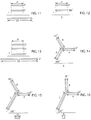
- Figs. 11 and 13 The effect of the reactive current from varying numbers of inverters 15 is illustrated, for example in Figs. 11 and 13 . It is known that an alternating current may be represented as a phasor quantity having an amplitude and an angle.
- Fig. 11 two inverters 15 are connected to the DC bus and the reactive current generated by each of the inverters 15 is represented as a current having a magnitude equal to "A" and an angle of zero degrees.
- the resulting reactive current at the output of the converter 11 has a magnitude equal to "2A" or twice the magnitude of each of the inverters 15 at an angle of zero degrees.
- Fig. 11 The effect of the reactive current from varying numbers of inverters 15 is illustrated, for example in Figs. 11 and 13 . It is known that an alternating current may be represented as a phasor quantity having an amplitude and an angle.
- Fig. 11 two inverters 15 are connected to the DC bus and the reactive current generated by each of the inverters 15
- three inverters 15 are connected to the DC bus and the reactive current generated by each of the inverters 15 is represented as a current having a magnitude equal to "A" and an angle of zero degrees.
- the resulting reactive current at the output of the converter 11 has a magnitude equal to "3A” or three times the magnitude of each of the inverters 15 at an angle of zero degrees.
- the phase angle of the reactive current generated from each of the inverters 15 is controlled such that the total reactive current on the shared DC bus 13 is reduced.
- Figs. 12 and 14 the effect of controlling the phase angle of the reactive current on the total reactive current is illustrated.
- Fig. 12 two inverters 15 are connected to the DC bus.
- the carrier phase angle of the first inverter 15 is set to zero degrees, and the reactive current generated by a first inverter 15 has a magnitude equal to "A" and an angle of zero degrees.
- the carrier phase angle of the second inverter 15 is set to ninety degrees, and the reactive current generated by the second inverter 15 has a magnitude equal to "A" and an angle of one hundred eighty degrees. Consequently, the reactive current generated by the second inverter cancels the reactive current generated by the first inverter and the resulting reactive current on the shared DC bus 13 is zero.
- three inverters 15 are connected to the DC bus.
- the carrier phase angle of the first inverter is set to zero degrees, and the reactive current generated by the first inverter 15 has a magnitude equal to "A" and an angle of zero degrees.
- the carrier phase angle of the second inverter is set to sixty degrees, and the reactive current generated by the first inverter 15 has a magnitude equal to "A" and an angle of one hundred twenty degrees.
- the carrier phase angle of the third inverter is set to one hundred twenty degrees, and the reactive current generated by the third inverter 15 has a magnitude equal to "A" and an angle of two hundred forty degrees. Consequently, the reactive currents generated by the three inverters cancel each other and the resulting reactive current on the shared DC bus 13 is zero.
- Figs. 12 and 14 represent idealized cancellation of reactive current and actual magnitudes and phases of the reactive currents generated by the inverters may vary.
- the magnitude of the resulting reactive current on the shared DC bus 13 is less than magnitude of the reactive current that would be present if any one of the inverters 15 is operating by itself.
- a preset value of the carrier phase angle may be assigned to each inverter 15 connected to the DC bus 13.
- the memory device 40, 50 in each of the remote devices 8, 10 may store the assigned carrier phase angle and the respective processor 38, 48 may retrieve the stored value for generation of the carrier signal.
- the value of the carrier phase angle may be selected as a function of the switching frequency or multiples thereof, the output frequency or multiples thereof, the number of remote devices 8, 10 connected to the common DC bus 24, the operating mode of a motor 16, 20 controlled by one of the remote devices 8, 10, or a combination thereof.
- the value of the carrier phase angle may be dynamically determined for each of the remote devices 8, 10.
- the memory device 40, 50 in each of the remote devices 8, 10 may have, for example, a look-up table in which multiple carrier phase angle values are stored.
- the carrier phase angle for each of the remote devices 8, 10 may be a first value if two inverter sections 32, 42 are connected to the DC bus 24 and a different value for each additional inverter section that is connected to the DC bus 24.
- three or more inverter sections may be connected but not all enabled at the same time to control their respective AC motor.
- the communication media 17 between processors may transmit data indicating the number of inverter sections that are currently enabled.
- the carrier phase angle for each device may be dynamically updated as different inverter sections are enabled and disabled. Further, the switching frequency of different inverter sections 32, 42 may be set to different values.
- the communication media 17 may also transmit data indicating the switching frequency of each inverter section.
- the inverter sections 32, 42 may then determine a carrier phase angle for each inverter section as a function of the number of inverter sections 32, 42 having either the same switching frequency or switching frequencies at multiples of each other.
- the processor 38, 48 in each remote device 8, 10 determines the carrier phase angle for the respective device.
- each of the processors 38, 48 transmit the operating status of the device to a master processor, which may be, for example, the processor 21 in the converter 27, and the master processor determines the carrier phase angle for each device and transmits the carrier phase angle to the respective devices.
- a master processor which may be, for example, the processor 21 in the converter 27, and the master processor determines the carrier phase angle for each device and transmits the carrier phase angle to the respective devices.
- the processor 38, 48 may measure the current present on the DC bus 24 and determine the carrier phase angle of each of the devices.
- the processor 38, 48 receives a feedback signal corresponding to the current present on the DC bus 24.
- the processor 38, 48 determines the spectral content of the feedback signal which contains amplitude information for varying frequencies present on the DC bus 24.
- the spectral content may be determined, for example, using a fourier transform, which may be a function of the output frequency and/or the switching frequency.
- a high frequency component of the current may be identified from the spectral content, for example, according to the component having the greatest amplitude.
- the phase of the identified frequency component may then be determined.
- Multiple processors 38, 48 communicate between each other the respective amplitude and/or phase of the identified frequency component to be compensated.
- the magnitude of the reactive current may be estimated as a function of the operating parameters conditions of each inverter section 32, 42.
- the processor 38, 42 receives a reference signal identifying desired operation of the motor 16 which is used to control operation of the motor drive 9.
- the reference signal may be, for example, a desired torque, speed, or angular position of the motor.
- the program generates, for example, an internal torque or current reference which is provided to a current regulator.
- the current regulator generates the desired voltage reference signal 102, 112 provided to the PWM module.
- each processor 38, 42 may be configured to determine an expected magnitude of reactive current.
- the carrier phase angle for each inverter section 32, 42 may then be determined to provide the best reduction of total reactive current on the DC bus 24 as a function of the measured current, estimated current, or a combination thereof.
- three inverters 15 are connected to the DC bus 13. Each of the inverters 15 determine that they are generating a reactive current at substantially the same frequency with magnitudes of "A", "B", and "C".
- the carrier phase angles of the inverters are set such that the phase angle of the respective reactive currents are zero degrees, one hundred twenty degrees, or two hundred forty degrees, as discussed above with respect to Fig. 14
- the resulting reactive current may have, for example, a magnitude equal to "D" at zero degrees as shown in Fig. 15 .
- the magnitude of "D" is less than the largest magnitude of the reactive current generated by any one of the inverters 15, it may not be the best obtainable reduction in reactive current.
- the carrier phase angle of the inverters 15 may be set such that the phase angle of each reactive current is zero degrees, ninety degrees, and two hundred thirty degrees.
- the resulting reactive current on the DC bus has a magnitude of "E” at zero degrees, where the magnitude of "E” is less than the magnitude of "D".
- the carrier phase angle may also be determined as a function of the magnitude of the reactive current generated by the inverters 15.
- one of the processors may be configured to generate carrier phase angles for each inverter 15.
- a control routine receives a reference corresponding, for example, to a desired magnitude of reactive current or a desired percentage reduction in the reactive current.
- the reactive current either measured or estimated at each inverter 15 is transmitted to the processor generating carrier phase angles.
- the control routine then generates carrier phase angles at which each inverter is to operate as a function or the reactive current and the reference signal.
- the carrier phase angle may be utilized to reduce conducted emissions generated by the inverters 15.
- the high frequency content of the reactive current may result in radiated and/or conducted emissions that are coupled back to the AC input voltage.
- leakage currents may be established through capacitive coupling between leads and the ground connections. If left unmitigated, these conducted emissions could interfere with other electrical devices receiving the same input voltage or connected elsewhere within the facility.
- the carrier phase angles of two inverters 15 operating under substantially identical operating conditions are set one hundred eighty degrees apart from each other, the emissions generated by the first inverter will offset the emissions generated by the second inverter. If more than two inverters 15 exist in the system, the carrier phase angle of a portion of the inverters 15 may be set to zero degrees and the carrier phase angle of the remaining inverters 15 may be set to one hundred eighty degrees.
- the reactive current may be amplified by setting the carrier phase angle of a first inverter 15 to zero degrees and a second inverter 15 to one hundred eighty degrees.
- the processor configured to generate carrier phase angles for each inverter 15 may further monitor the magnitude of current supplied by each inverter 15 to its corresponding motor to determine a desired operating mode. If for example, the current output to the motor is below a threshold, such as fifty percent of rated current for the inverter 15, the carrier phase angle may be controlled to minimize the conducted emissions generated by the inverter 15. If, however, the current output to the motor is above the threshold, the carrier phase angle may be controlled to minimize the reactive current on the DC bus 13.
- the processor may generate a transitional carrier signal during a transition between carrier phase angles.
- the inverter 15 is in a first operating mode and has determined a first carrier phase angle at which the carrier signal is to be generated.
- the operating conditions of the system change, for example, due to the motor controlled by an inverter 15 switching between motoring and regenerative operation or by the addition or subtraction of an enabled inverter 15 connected to the DC bus 13.
- a new carrier phase angle is determined for operation in a second operating mode.
- the carrier signal is changed from a triangle waveform to a ramp waveform.
- the carrier signal preferably remains a ramp waveform for one period 210 and then reverts to a triangle waveform having the new carrier phase angle during the third period 220. This transition between operating modes reduces undesirable step changes in the output of the inverter 15.
Description
- The subject matter disclosed herein relates generally to a system having a direct current (DC) bus which is shared by multiple inverters and, more specifically, to a system for reducing the amplitude of reactive current present on the DC bus as a result of the multiple inverters.
- As is known to those skilled in the art, a motor drive receives an input voltage and converts the input voltage to a suitable output voltage for controlling operation of a motor. In an Alternating Current (AC) motor drive, a three phase AC voltage is typically available at, for example, 230 V or 460 V as the input voltage. The motor drive includes a converter section that rectifies the AC input voltage into a Direct Current (DC) voltage. The DC voltage is present across a first rail and a second rail of a DC bus in the motor drive. An inverter section includes switches, such as transistors, thyristors, or silicon-controlled rectifiers to convert the DC voltage on the DC bus into an AC voltage output at the desired magnitude and frequency to control operation of the motor. It is also known that the converter, DC bus, and inverter sections may be enclosed in a single housing as a centralized motor drive configured to be mounted in a control cabinet. Alternately, a portion of the motor drive, such as the inverter section, may be included in
a separate housing or integrated into the motor housing and located by the motor to be controlled. The converter section may be included a housing configured to be mounted in the control cabinet. A DC link including a DC bus cable, as well as, inductive or capacitive elements connects the converter section to one or more distributed inverter sections. - The motor drive often utilizes a pulse-width modulation (PWM) routine to control the switches in the inverter section. The switches alternately connect and disconnect either the first or second rail of the DC bus to the AC output. The resulting output is, therefore, either zero volts or fully on at the voltage level present on the DC bus. In order to vary the magnitude of the output voltage, the PWM routine repeatedly executes at a predetermined interval, sometimes referred to as a carrier period, where the inverse of the carrier period is the carrier frequency. The PWM routine receives a reference signal corresponding to the desired output voltage magnitude and controls the switches such that the DC bus is connected to the output for a portion of the carrier period. Thus, during each carrier period, the output is on for a percentage of the carrier period and off for the remaining percentage of the carrier period and an average voltage magnitude for each carrier period results. By varying the percentage of the carrier period that each switch is on or off, the average voltage magnitude varies such that it corresponds to the reference signal input to the PWM routine. If the fundamental frequency of the desired AC voltage is much less than the carrier frequency, the resulting output voltage waveform approximates the desired AC voltage.
- However, the high frequency switching generates undesirable reactive currents at the carrier frequency and harmonics, or multiples, thereof, which may be present, for example, on the DC bus. The reactive current present on the DC bus is of particular concern in a distributed motor drive. The inverter sections may be a significant distance from the converter section, and the DC bus cable and other reactive DC link components such as inductors and capacitors present a significant impedance to the high frequency reactive currents. The reactive currents are dissipated, at least in part, as power losses in the DC link components as a result of these impedances. , In addition, if multiple inverter sections are connected to a single converter, each generates reactive currents which are transferred to the DC bus, increasing the potential maximum amplitude of the reactive currents.
- Historically, it has been known to increase the size of the DC link components for the DC bus between the converter section and the inverter sections to accommodate the increased current. However, in some applications the inverter sections are mounted on the machines that they control and distributed about a controlled machine or process. Thus, tens or hundreds of feet of cabling may be required to connect each inverter section to the converter section. An increase in the wire gauge or other DC link components results in a significant increase in cost and potentially undesirable weight to the controlled system.
- Thus, it would be desirable to control the switching of each inverter on a shared DC bus to reduce the overall reactive current present on the DC bus.
-
US 2005/225270 A1 discloses a variable speed drive having a converter to convert an AC voltage to a DC voltage, a DC link to filter and store energy from the converter, and a plurality of inverters. Each inverter is configured to convert a DC voltage to an AC voltage and is electrically connected in parallel to the DC link. An interleaved pulse width modulation control technique is used to control the operation of the plurality of inverters and possibly the converter to lower the RMS ripple current in the DC link. -
US 2012/153882 A1 discloses an inverter executing a PWM routine being configured to synchronize the switching periods of the PWM routine to an external signal. The external signal is generated by another inverter, a converter, or a high level controller. The external signal is generated periodically, and the switching period is resynchronized to the external signal each time the external signal is received. Either the start time or the midpoint of the switching period may be aligned with external signal. Further, the external signal is sent to multiple inverters. - It is therefore the object of the present invention to provide an improved system for reducing a reactive current present on a direct current bus.
- This object is solved by the subject matter of the independent claim.
- Preferred embodiments are defined by the dependent claims.
- The subject matter disclosed herein describes a system configured to reduce the amplitude of reactive current present on a DC bus shared by multiple inverters. The system may include one processor configured to control multiple inverters or multiple processors each configured to control a respective inverter. A synchronizing signal is generated by one of the processors to coordinate the start of each switching period for the modulation routines of each inverter. A carrier phase angle is determined for each of the inverters which defines the point within a carrier signal used by the modulation routine of each inverter that corresponds to the start of the switching period. The modulation routine of each inverter generates a reactive current, one component of which is known as a ripple current, on the shared DC bus. By controlling the carrier phase angle for each inverter, the reactive current of a first inverter may be generated at a phase angle that is offset from the phase angle of the reactive current generated by a second inverter. As a result, the reactive current from the first inverter cancels at least a portion of the reactive current from the second inverter, reducing the total reactive current present on the DC bus.
- According to one embodiment of the invention, a system for reducing a reactive current present on a DC bus is disclosed. The DC bus has a first voltage rail and a second voltage rail and is configured to have a DC voltage potential present between the first voltage rail and the second voltage rail. The system includes a plurality of inverters, and each inverter includes an input configured to connect to the first and second voltage rails of the DC bus, an output configured to connect to an alternating current (AC) load, and a plurality of switching devices. Each switching device is controlled by a switching signal to alternately connect and disconnect the input to the output.
- A modulation module is configured to execute at a periodic interval. During each periodic interval the modulation module determines each of the switching signals as a function of a carrier signal that repeats within the periodic interval and at least one voltage reference signal. Each carrier signal is defined at least in part by a carrier phase angle, and each voltage reference signal corresponds to a desired output voltage for each phase of the AC load. A synchronizing signal is in communication with each of the modulation modules and is used by each modulation module to start its corresponding periodic interval at substantially the same time.
- A controller generates the carrier phase angle for each inverter. The carrier phase angle for each inverter is determined such that a first reactive current generated by the plurality of switching devices which alternately connect and disconnect the input to the output in a first inverter is at least partially cancelled by a second reactive current generated by the plurality of switching devices which alternately connect and disconnect the input to the output in a second inverter.
- According to another embodiment of the invention, an inverter for connection to a common DC bus is disclosed. The common DC bus has a first voltage rail, a second voltage rail, a DC voltage potential present between the first voltage rail and the second voltage rail, and at least one additional inverter connected to the common DC bus. The inverter includes a first input configured to receive a synchronizing signal, a second input configured to receive an indication of the number of additional inverters connected to the common DC bus, a DC bus input configured to connect to the first and second voltage rails of the common DC bus, an output configured to connect to an AC load, a memory device configured to store an identifier corresponding to each inverter, a controller configured to generate a carrier phase angle, and a plurality of switching devices controlled by a switching signal to alternately connect and disconnect the DC bus input to the output. The carrier phase angle is determined as a function of the number of additional inverters connected to the common DC bus and of the identifier.
- A modulation module is configured to execute at a periodic interval. A start time of each periodic interval is defined, at least in part, by the synchronizing signal, and during each periodic interval, the modulation module determines each of the switching signals as a function of a carrier signal that repeats within the periodic interval and at least one voltage reference signal. Each carrier signal is defined at least in part by the carrier phase angle and corresponds to a desired output voltage for each phase of the AC load.
- According to yet another embodiment of the invention, a method of controlling a plurality of inverters, where each inverter converts a DC voltage from a shared DC bus to an AC voltage, is disclosed. According to the method, a synchronizing signal is generated with a controller, and the synchronizing signal defines a start of a periodic interval for a modulation routine for each of the inverters. A carrier phase angle is determined for each of the inverters with the controller such that a first reactive current generated by a first inverter is at least partially cancelled by a second reactive current generated by a second inverter. A carrier signal is generated for the modulation routine for each of the inverters with the controller as a function of the carrier phase angle. The modulation module is executing for each inverter to determine a plurality of switching signals as a function of the carrier signal and of at least one voltage reference signal. Each voltage reference signal corresponds to a desired output voltage for each phase of the AC voltage and each switching signal controls a switching device to alternately connect and disconnect the DC bus to an output of the inverter.
- These and other advantages and features of the invention will become apparent to those skilled in the art from the detailed description and the accompanying drawings. It should be understood, however, that the detailed description and accompanying drawings, while indicating preferred embodiments of the present invention, are given by way of illustration and not of limitation. Many changes and modifications may be made within the scope of the present invention, and the invention includes all such modifications.
- Various exemplary embodiments of the subject matter disclosed herein are illustrated in the accompanying drawings in which like reference numerals represent like parts throughout, and in which:
-
FIG. 1 is a block diagram representation of an exemplary system incorporating one embodiment of the present invention; -
FIG. 2 is a schematic representation of a multi-axis motor drive incorporating one embodiment of the present invention; -
FIG. 3 is a schematic representation of a distributed motor drive system incorporating one embodiment of the present invention; -
FIG. 4 is a schematic representation of an inverter section from one of the inverters ofFig. 3 ; -
FIG. 5 is a graphical representation of a pair of carrier signals aligned with each other according to one embodiment of the invention; -
FIG. 6 is a graphical representation of a pair of carrier signals offset from each other according to one embodiment of the invention; -
FIG. 7 is a graphical representation of the current drawn by two motors where each motor is in a motoring mode of operation and the pair of carrier signals are aligned with each other; -
FIG. 8 is a graphical representation of the current drawn by two motors where each motor is in a motoring mode of operation and the pair of carrier signals are offset from each other; -
FIG. 9 is a graphical representation of the current drawn by two motors where one motoring is in a regenerative mode of operation and the other motor is in a motoring mode of operation and the pair of carrier signals are aligned with each other; -
FIG. 10 is a graphical representation of the current drawn by two motors where one motoring is in a regenerative mode of operation and the other motor is in a motoring mode of operation and the pair of carrier signals are offset from each other; -
FIG. 11 is a vector representation of the reactive current generated by two inverters where the phase angle of the reactive current is in phase with each other; -
FIG. 12 is a vector representation of the reactive current generated by two inverters where the phase angle of the reactive current is out of phase with each other; -
FIG. 13 is a vector representation of the reactive current generated by three inverters where the phase angle of the reactive current is in phase with each other; -
FIG. 14 is a vector representation of the reactive current generated by three inverters where the phase angle of the reactive current is out of phase with each other; -
FIG. 15 is a vector representation of the reactive current generated by three inverters where the magnitude of each reactive current varies and the phase angle of the reactive current are out of phase with each other; -
FIG. 16 is a vector representation of the reactive current generated by three inverters where the magnitude of each reactive current varies and the phase angle of the reactive current are out of phase with each other; and -
FIG. 17 is a graphical representation of a carrier signal transitioning between operating modes according to one embodiment of the present invention. - In describing the various embodiments of the invention which are illustrated in the drawings, specific terminology will be resorted to for the sake of clarity. However, it is not intended that the invention be limited to the specific terms so selected and it is understood that each specific term includes all technical equivalents which operate in a similar manner to accomplish a similar purpose. For example, the word "connected," "attached," or terms similar thereto are often used. They are not limited to direct connection but include connection through other elements where such connection is recognized as being equivalent by those skilled in the art.
- Turning initially to
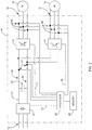
Fig. 1 , a block diagram representation of a system includingmultiple inverters 15 connected to asingle DC bus 13 is illustrated. According to the illustrated embodiment, aconverter 11 receives power in a first form and provides it to theDC bus 13. The input may be a DC voltage or an AC voltage, where the AC voltage is either single phase or multi-phase. Theconverter 11 is configured to supply a regulated DC voltage on theDC bus 13. The system includes at least afirst inverter 15 and asecond inverter 15, but may include any number ofadditional inverters 15. Eachinverter 15 converts the DC voltage present on theDC bus 13 to an AC voltage for use by an electrical load.Communication media 17 extends between theconverter 11 and eachinverter 15. Thecommunication media 17 may be a single electrical conductor, multiple electrical conductors, a network cable configured to transmit data packets, or any othersuitable communication media 17 configured to transmit data between the devices according to application requirements. Optionally, thecommunication media 17 may extend only between theinverters 15. - Turning next to
Fig. 2 , one embodiment of the present invention includes amotor drive 9 connected to a three phaseAC input voltage 12. Themotor drive 9 is configured withmultiple inverter sections multiple outputs motor drive 9 generates afirst output 14, illustrated as a three phase AC output voltage, to control afirst motor 16, and asecond output 18, also illustrated as a three phase AC output voltage, to control asecond motor 20. It is contemplated that the output voltage, 14 or 18, could be a single phase AC output voltage, a multi-phase AC output voltage, or a DC voltage, as required by the motor connected to the drive without deviating from the scope of the invention. - The
AC input voltage 12 is converted to a DC voltage present on theDC bus 24 by aconverter section 22. The DC voltage potential is present between afirst rail 28 and asecond rail 30 of theDC bus 24. ADC bus capacitor 26 is connected between the first and second rails, 28 and 30, to reduce the magnitude of the reactive voltage resulting from converting the AC voltage to a DC voltage. It is understood that theDC bus capacitor 26 may be a single capacitor or multiple capacitors connected in parallel, in series, or a combination thereof. The magnitude of the voltage potential between the first and second rails, 28 and 30, is generally about equal to or greater than the magnitude of the peak of the AC input voltage. It is further contemplated that the DC bus may include more than two rails including, but not limited to multiple positive rails, multiple negative rails, a neutral rail, or combinations thereof as would be present, for example, in a multilevel converter. - A
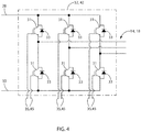
single converter section 22 is provided between theinput voltage 12 and theDC bus 24 while twoinverter sections common DC bus 24 and theirrespective output converter section 22 may be either passive or active, where a passive rectifier utilizes electronic devices such as diodes, which require no control signals, to convert the AC voltage to a DC voltage and an active converter utilizes, for example, transistors, which receiveswitching signals 25 to turn on and off, to convert theinput voltage 12 to the desired DC voltage. Referring also toFig. 4 , eachinverter section multiple switches 31 which selectively connect one phase of eachoutput first rail 28 or thesecond rail 30. Eachswitch 31 may be a transistor and further include adiode 33 connected in parallel to the transistor. Eachswitch 31 receives aswitching signal output first rail 28 or thesecond rail 30 of theDC bus 24. - The
processor 38 executes a program stored on amemory device 40, where the program includes a series of instructions executable on theprocessor 38 to control operation of themotor drive 9. Each program receives a reference signal identifying desired operation of themotor 16 connected to themotor drive 9. Theprocessor 38 also receives feedback signals from voltage and/or current sensors positioned within themotor drive 9.Sensors 34 may be provided to measure the voltage and/or current on theDC bus 24, andadditional sensors Figs. 7-10 . Theprocessor 38 also executes a modulation routine, such as pulse width modulation (PWM), to generate switching signals, 35 or 45, to control theswitches 31 of eachinverter section - Turning next to
Fig. 3 , another embodiment of the present invention includes aconverter 27, connected to the three phaseAC input voltage 12. ADC bus 24 distributes the DC voltage from theconverter 27 to a first remote device 8 and a secondremote device 10. The first and second remote devices, 8 and 10, may be, for example, distributed motor drives. The first remote device 8 generates afirst output 14, illustrated as a three phase AC output voltage, to control afirst motor 16, and the secondremote device 10 generates asecond output 18, also illustrated as a three phase AC output voltage, to control asecond motor 20. It is contemplated that still other embodiments of the invention may include various configurations of converters, inverters, and/or multiple axis motor drives connected to a common DC bus without deviating from the scope of the invention. It is further contemplated that the output voltage, 14 or 18, for the first or second remote device, 8 or 10 respectively, could be a single phase AC output voltage, a multi-phase AC output voltage, or a DC voltage, as required by the motor connected to the drive without deviating from the scope of the invention. - A
converter section 22 converts theAC input voltage 12 to a DC voltage potential present on theDC bus 24. Theconverter section 22 may be either passive or active, where a passive converter utilizes electronic devices such as diodes, which require no control signals, to convert the AC voltage to a DC voltage and an active converter utilizes, for example, transistors, which receiveswitching signals 25 to turn on and off, to convert the AC voltage to a DC voltage. The DC voltage potential is present between afirst rail 28 and asecond rail 30 of theDC bus 24. ADC bus capacitor 26 is connected between the first and second rails, 28 and 30, to reduce the magnitude of the reactive voltage resulting from converting the AC voltage to a DC voltage. It is understood that theDC bus capacitor 26 may be a single capacitor or multiple capacitors connected in parallel, in series, or a combination thereof. Theconverter section 22 includes aprocessor 21 configured to execute a program stored on amemory device 23. If theconverter section 22 is active, the processor may be configured to generate the switching signals 25. The processor may also be configured to generate a synchronizing signal to be output to each of the remote devices via, for example, thecommunication media 17. - Each of the
remote devices 8, 10 includes aDC bus 24 electrically connected to theDC bus 24 of theconverter 27. Referring also toFig. 4 , eachinverter section multiple switches 31 which selectively connect one of the output phases 14 to either thefirst rail 28 or thesecond rail 30. Eachswitch 31 may be a transistor and further include adiode 33 connected in parallel to the transistor. Eachswitch 31 receives aswitching signal output first rail 28 or thesecond rail 30 of theDC bus 24. Eachremote device 8, 10 also includes aprocessor memory device processor remote device 8, 10. Each program receives a reference signal identifying desired operation of themotor remote device 8, 10. The reference signal may be, for example, a desired speed or torque and may be transmitted viacommunication media 17 from theconverter 27 or from another controller. Eachprocessor Sensors DC bus 24, andadditional sensors outputs Figs. 7-10 . Theprocessor inverter section - In operation, a controller executes to coordinate the modulation routines of each
inverter section DC bus 24. According to one embodiment of the invention, as illustrated inFig. 2 , asingle processor 38 may be used. Theprocessor 38 may be configured to execute the modulation routines and generate switchingsignals inverter section processor 38 may be configured to coordinate operation of the modulation routines. According to another embodiment of the invention, as illustrated inFig. 2 , theconverter 27 and eachremote device 8, 10 may each include aprocessor processors other processors processors Fig. 3 ; however, the illustrated embodiment is not meant to be limiting. - One of the processors in the system is configured to be a master processor. For illustration, the
processor 21 in theconverter 27 will be designated as the master processor. Optionally, one of theprocessors master processor 21 generates a synchronizing signal, which is transmitted to each of theremote devices 8, 10. The synchronizing signal is used by each of theremote devices 8, 10 to coordinate their respective modulation routines. The synchronizing signal may be any suitable signal, such as a single pulse or a counter preset value. The synchronizing signal may be sent initially upon power up, at the start of operation of aremote device 8, 10, at a periodic interval or any combination thereof. - Referring also to
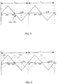
Fig. 5 , modulation routines repeatedly execute at a predefined interval known as a switching period, T, which is the inverse of the switching frequency. Eachremote device 8, 10 uses the synchronizing signal to coordinate the start of the switching period T, of its respective modulation routine with the otherremote devices 8, 10. As a result, the start of the switching period, T, for eachremote device 8, 10 begins at substantially the same time. Once coordinated, eachprocessor remote device 8, 10 is substantially the same. Once execution has begun, the modulation routines for eachremote device 8, 10 continue to operation in tandem. However, slight variations in clock frequencies or component tolerances may cause variations in the actual duration of the switching period, T, for each of theremote devices 8, 10. Periodically transmitting the synchronizing signal from themaster processor 21 allows theprocessors remote device 8, 10 to resynchronize the start of their respective switching period, T, with the otherremote devices 8, 10. Optionally, eachprocessor processors - Referring next to
Figs. 5 and 6 , eachprocessor remote device 8, 10 generates acarrier signal first inverter section 32 generates afirst carrier signal 100, and the modulation routine of thesecond inverter section 42 generates asecond carrier signal 110. Eachreference signal carrier signal Fig. 5 , each of the carrier signals 100, 110 have a carrier phase angle of zero degrees. Setting the carrier phase angle to a value other zero degrees, shifts thecarrier signal fig. 6 , the carrier phase angle of thefirst carrier signal 100 remains at zero degrees but the carrier phase angle of thesecond carrier signal 110 is set to ninety degrees. As a result, the periodic waveform is shifted by one quarter of the period, T. - Referring next to
Figs. 7-10 , theprocessor remote device 8, 10 executes the modulation routine to generate switchingsignals respective inverter section first processor 38 generates a firstvoltage reference signal 102a-c for each phase of theoutput 14 of the first remote device 8, and a control module executing on thesecond processor 48 generates a secondvoltage reference signal 112a-c for each phase of theoutput 18 of the secondremote device 10. Each of thevoltage reference signals 102a-c, 1 12a-c is compared against therespective carrier signal voltage reference signal 102a-c, 1 12a-c for one of the phases is greater than therespective carrier signal output DC bus 24. During the periods when each phase of theoutput DC bus 24, that phase conducts current 104, 114 to therespective motor remote device 8, 10. Exemplary waveforms for thecurrents 104a-c, 114a-c present on each phase of theoutput voltage reference signals 102a-c, 112a-c to the carrier signals 100, 110. The final waveform illustrates the DC bus current 120, IDC, present on theDC bus 24 as a result of the high frequency switching by each of theinverter sections remote devices 8, 10. - Each of the graphs in
Figs. 7-10 illustrates a different set of operating conditions for the tworemote devices 8, 10. For each of the exemplary operating conditions illustrated, theinverter sections remote device 8, 10 use the synchronizing signal to coordinate the start of the switching period, T, of its respective modulation routine, and the switching period, T, for eachinverter section Fig. 7 , each of themotors remote devices 8, 10 are operating in a motoring mode, and the carrier phase angle for the carrier signals 100, 110 generated by eachprocessor carrier signal voltage references 102a-c, 112a-c for each of therespective inverter sections output currents 104a-c, 114a-c for eachremote device 8, 10 that are substantially the same. As a result, the reactive current generated by eachinverter section inverter section - In contrast, each of the
motors remote devices 8, 10 are still operating in a motoring mode inFig. 8 ; however, the carrier phase angle of thefirst carrier signal 100 is set to zero degrees and the carrier phase angle of thesecond carrier signal 110 is set to ninety degrees. Thecurrents 104a-c generated by thefirst inverter section 32 are the same as illustrated inFig. 7 . However, theoutput currents 114a-c generated by thesecond inverter section 42 are shifted in phase as a result of the carrier phase angle offset. As a result, the reactive currents generated by eachinverter section second inverter section 42 at least partially cancels the reactive current generated by thefirst inverter section 32. The DC bus current 120, therefore, has a lower total reactive current present compared to the reactive current that would be generated by eitherinverter section - In
Figs. 9 and10 , themotor 16 controlled by the first remote device 8 is operating in a motoring mode; however, themotor 20 controlled by the secondremote device 10 is operating in a regenerative mode. The inventors observed that the effects on reactive current are reversed when compared toFigs. 7 and8 in which bothmotors Fig. 9 , the carrier phase angle for the carrier signals 100, 110 generated by eachprocessor second inverter section 42 is out of phase with the reactive current generated by thefirst inverter section 32 and, therefore, the reactive current generated by thesecond inverter section 42 at least partially cancels the reactive current generated by thefirst inverter section 32. The DC bus current 120, therefore, has a lower total reactive current present compared to the reactive current that would be generated by eitherinverter section - In
Fig. 10 , the carrier phase angle of thefirst carrier signal 100 is set to zero degrees and the carrier phase angle of thesecond carrier signal 110 is set to ninety degrees. Although theoutput currents 114a-c generated by thesecond inverter section 42 are still shifted as a result of the carrier phase angle offset, the reactive current generated by eachinverter section inverter section remote device 8, 10 is a function of whether the correspondingmotor remote device 8, 10 is operating in a motoring mode or in a regenerating mode. In addition, eachmotor motor motor processor remote device 8, 10 continue to cancel each other regardless of the operating mode of themotors - The carrier phase angle selected for each of the carrier signals 100, 110 is also a function of the number of inverter sections connected to the common DC bus. Referring again to
Fig. 1 , any number ofinverters 15 may be connected to theDC bus 13. The total current, IDC, present on the sharedDC bus 13 is equal to the sum of the currents (e.g., I1 + I2 + · · · + In) required by each of theinverters 15. Similarly, the reactive current generated by each of theinverters 15 is also present on theDC bus 13 and the total reactive current present on the sharedDC bus 13 is the sum of the reactive currents generated by each of theinverters 15. The effect of the reactive current from varying numbers ofinverters 15 is illustrated, for example inFigs. 11 and 13 . It is known that an alternating current may be represented as a phasor quantity having an amplitude and an angle. InFig. 11 , twoinverters 15 are connected to the DC bus and the reactive current generated by each of theinverters 15 is represented as a current having a magnitude equal to "A" and an angle of zero degrees. The resulting reactive current at the output of theconverter 11 has a magnitude equal to "2A" or twice the magnitude of each of theinverters 15 at an angle of zero degrees. InFig. 13 , threeinverters 15 are connected to the DC bus and the reactive current generated by each of theinverters 15 is represented as a current having a magnitude equal to "A" and an angle of zero degrees. The resulting reactive current at the output of theconverter 11 has a magnitude equal to "3A" or three times the magnitude of each of theinverters 15 at an angle of zero degrees. - By controlling the carrier phase angle of each of the carrier signals in the
inverters 15, the phase angle of the reactive current generated from each of theinverters 15 is controlled such that the total reactive current on the sharedDC bus 13 is reduced. Referring next toFigs. 12 and 14 , the effect of controlling the phase angle of the reactive current on the total reactive current is illustrated. InFig. 12 , twoinverters 15 are connected to the DC bus. The carrier phase angle of thefirst inverter 15 is set to zero degrees, and the reactive current generated by afirst inverter 15 has a magnitude equal to "A" and an angle of zero degrees. The carrier phase angle of thesecond inverter 15 is set to ninety degrees, and the reactive current generated by thesecond inverter 15 has a magnitude equal to "A" and an angle of one hundred eighty degrees. Consequently, the reactive current generated by the second inverter cancels the reactive current generated by the first inverter and the resulting reactive current on the sharedDC bus 13 is zero. InFig. 14 , threeinverters 15 are connected to the DC bus. The carrier phase angle of the first inverter is set to zero degrees, and the reactive current generated by thefirst inverter 15 has a magnitude equal to "A" and an angle of zero degrees. The carrier phase angle of the second inverter is set to sixty degrees, and the reactive current generated by thefirst inverter 15 has a magnitude equal to "A" and an angle of one hundred twenty degrees. The carrier phase angle of the third inverter is set to one hundred twenty degrees, and the reactive current generated by thethird inverter 15 has a magnitude equal to "A" and an angle of two hundred forty degrees. Consequently, the reactive currents generated by the three inverters cancel each other and the resulting reactive current on the sharedDC bus 13 is zero.Figs. 12 and 14 represent idealized cancellation of reactive current and actual magnitudes and phases of the reactive currents generated by the inverters may vary. By controlling the carrier phase angle and, in turn, controlling the phase angle of the reactive current, at least a portion of the reactive current from thefirst inverter 15 is cancelled by the reactive current from thesecond inverter 15. Thus, the magnitude of the resulting reactive current on the sharedDC bus 13 is less than magnitude of the reactive current that would be present if any one of theinverters 15 is operating by itself. - According to one embodiment of the invention, a preset value of the carrier phase angle may be assigned to each
inverter 15 connected to theDC bus 13. Referring again toFig. 3 , thememory device remote devices 8, 10 may store the assigned carrier phase angle and therespective processor remote devices 8, 10 connected to thecommon DC bus 24, the operating mode of amotor remote devices 8, 10, or a combination thereof. - According to another embodiment of the invention, the value of the carrier phase angle may be dynamically determined for each of the
remote devices 8, 10. Thememory device remote devices 8, 10 may have, for example, a look-up table in which multiple carrier phase angle values are stored. The carrier phase angle for each of theremote devices 8, 10 may be a first value if twoinverter sections DC bus 24 and a different value for each additional inverter section that is connected to theDC bus 24. Similarly, three or more inverter sections may be connected but not all enabled at the same time to control their respective AC motor. Thecommunication media 17 between processors may transmit data indicating the number of inverter sections that are currently enabled. Thus, the carrier phase angle for each device may be dynamically updated as different inverter sections are enabled and disabled. Further, the switching frequency ofdifferent inverter sections communication media 17 may also transmit data indicating the switching frequency of each inverter section. Theinverter sections inverter sections processor remote device 8, 10 determines the carrier phase angle for the respective device. According to another embodiment of the invention, each of theprocessors processor 21 in theconverter 27, and the master processor determines the carrier phase angle for each device and transmits the carrier phase angle to the respective devices. - According to yet another embodiment of the invention, the
processor DC bus 24 and determine the carrier phase angle of each of the devices. Theprocessor DC bus 24. Theprocessor DC bus 24. The spectral content may be determined, for example, using a fourier transform, which may be a function of the output frequency and/or the switching frequency. A high frequency component of the current may be identified from the spectral content, for example, according to the component having the greatest amplitude. The phase of the identified frequency component may then be determined.Multiple processors - It is further contemplated that the magnitude of the reactive current may be estimated as a function of the operating parameters conditions of each
inverter section processor motor 16 which is used to control operation of themotor drive 9. The reference signal may be, for example, a desired torque, speed, or angular position of the motor. The program generates, for example, an internal torque or current reference which is provided to a current regulator. The current regulator generates the desired voltage reference signal 102, 112 provided to the PWM module. Based on these desired operating conditions, the generated reference signals, the motor parameters, or a combination thereof, eachprocessor inverter section DC bus 24 as a function of the measured current, estimated current, or a combination thereof. With reference toFigs. 1 ,15, and 16 , threeinverters 15 are connected to theDC bus 13. Each of theinverters 15 determine that they are generating a reactive current at substantially the same frequency with magnitudes of "A", "B", and "C". If the carrier phase angles of the inverters are set such that the phase angle of the respective reactive currents are zero degrees, one hundred twenty degrees, or two hundred forty degrees, as discussed above with respect toFig. 14 , the resulting reactive current may have, for example, a magnitude equal to "D" at zero degrees as shown inFig. 15 . Although the magnitude of "D" is less than the largest magnitude of the reactive current generated by any one of theinverters 15, it may not be the best obtainable reduction in reactive current. For instance, with reference toFig. 16 , the carrier phase angle of theinverters 15 may be set such that the phase angle of each reactive current is zero degrees, ninety degrees, and two hundred thirty degrees. The resulting reactive current on the DC bus has a magnitude of "E" at zero degrees, where the magnitude of "E" is less than the magnitude of "D". Thus, the carrier phase angle may also be determined as a function of the magnitude of the reactive current generated by theinverters 15. - It is further contemplated that one of the processors may be configured to generate carrier phase angles for each
inverter 15. A control routine receives a reference corresponding, for example, to a desired magnitude of reactive current or a desired percentage reduction in the reactive current. The reactive current either measured or estimated at eachinverter 15 is transmitted to the processor generating carrier phase angles. The control routine then generates carrier phase angles at which each inverter is to operate as a function or the reactive current and the reference signal. - According to yet another embodiment of the invention, the carrier phase angle may be utilized to reduce conducted emissions generated by the
inverters 15. The high frequency content of the reactive current may result in radiated and/or conducted emissions that are coupled back to the AC input voltage. For example, leakage currents may be established through capacitive coupling between leads and the ground connections. If left unmitigated, these conducted emissions could interfere with other electrical devices receiving the same input voltage or connected elsewhere within the facility. If the carrier phase angles of twoinverters 15 operating under substantially identical operating conditions are set one hundred eighty degrees apart from each other, the emissions generated by the first inverter will offset the emissions generated by the second inverter. If more than twoinverters 15 exist in the system, the carrier phase angle of a portion of theinverters 15 may be set to zero degrees and the carrier phase angle of the remaininginverters 15 may be set to one hundred eighty degrees. - However, as previously discussed reactive currents are best reduced by carrier phase angles other than zero and one hundred eighty degrees. In fact, the reactive current may be amplified by setting the carrier phase angle of a
first inverter 15 to zero degrees and asecond inverter 15 to one hundred eighty degrees. Thus, the processor configured to generate carrier phase angles for eachinverter 15, may further monitor the magnitude of current supplied by eachinverter 15 to its corresponding motor to determine a desired operating mode. If for example, the current output to the motor is below a threshold, such as fifty percent of rated current for theinverter 15, the carrier phase angle may be controlled to minimize the conducted emissions generated by theinverter 15. If, however, the current output to the motor is above the threshold, the carrier phase angle may be controlled to minimize the reactive current on theDC bus 13. When the carrier phase angle of aninverter 15 is updated dynamically, it may result in an undesirable step change in the output of theinverter 15. Referring next toFig. 17 , the processor may generate a transitional carrier signal during a transition between carrier phase angles. During thefirst period 200, theinverter 15 is in a first operating mode and has determined a first carrier phase angle at which the carrier signal is to be generated. The operating conditions of the system change, for example, due to the motor controlled by aninverter 15 switching between motoring and regenerative operation or by the addition or subtraction of an enabledinverter 15 connected to theDC bus 13. A new carrier phase angle is determined for operation in a second operating mode. At the end of thefirst period 200, the carrier signal is changed from a triangle waveform to a ramp waveform. The carrier signal preferably remains a ramp waveform for oneperiod 210 and then reverts to a triangle waveform having the new carrier phase angle during thethird period 220. This transition between operating modes reduces undesirable step changes in the output of theinverter 15. - It should be understood that the invention is not limited in its application to the details of construction and arrangements of the components set forth herein. The invention is capable of other embodiments and of being practiced or carried out in various ways. Variations and modifications of the foregoing are within the scope of the present invention. It also being understood that the invention disclosed and defined herein extends to all alternative combinations of two or more of the individual features mentioned or evident from the text and/or drawings. All of these different combinations constitute various alternative aspects of the present invention. The embodiments described herein explain the best modes known for practicing the invention and will enable others skilled in the art to utilize the invention.
Claims (8)
- A system configured to reduce a reactive current present on a direct current, DC, bus (24), the DC bus having a first voltage rail and a second voltage rail wherein the DC bus is configured to have a DC voltage potential present between the first voltage rail and the second voltage rail, the system comprising:a plurality of inverters (15), with the reactive current including ripple currents originating from the plurality of inverters switchings, each inverter including:an input configured to connect to the first and second voltage rails of the DC bus,an output configured to connect to an alternating current, AC, load, wherein the AC load is a motor,a plurality of switching devices, each switching device controlled by a switching signal to alternately connect and disconnect the input to the output, anda modulation module configured to determine, at a periodic interval, each of the switching signals, wherein during each periodic interval the modulation module determines each of the switching signals as a function of a carrier signal that repeats each periodic interval and at least one voltage reference signal, wherein each carrier signal is defined, at least in part, by a carrier phase angle and each voltage reference signal corresponds to a desired output voltage for each phase of the AC load;a synchronizing signal in communication with each of the modulation modules, wherein the synchronizing signal is used by each modulation module to start its corresponding periodic interval at the same time;a controller configured to generate a carrier phase angle for each inverter,wherein the carrier phase angle for each inverter is dynamically updated during operation of the corresponding motor and is a function of whether the corresponding motor is operating in a motoring mode or in a regenerating mode,wherein the carrier signal is a first waveform during each of the motoring and regenerating modes, and the carrier signal is a second waveform, different from the first waveform, during at least one periodic interval (210) to transition between the motoring and regenerating modes; anda communication media (17) that extends between the controller and each inverter to transmit the carrier phase angle between the controller and each inverter such that a first reactive current generated by the plurality of switching devices alternately connecting and disconnecting the input to the output in a first inverter (32) is at least partially cancelled by a second reactive current generated by the plurality of switching devices alternately connecting and disconnecting the input to the output in a second inverter (42).
- The system of claim 1 wherein the controller includes a processor (21) configured to generate each of the carrier phase angles.
- The system of claim 1 or 2 wherein the processor (21) is further configured to generate each of the carrier phase angles to minimize the reactive current present on the DC bus (24).
- The system of any one of claims 1 to 3 wherein the processor (21) is further configured to generate each of the carrier phase angles to minimize the conducted emissions generated by each of the plurality of inverters.
- The system of any one of claims 1 to 4 wherein each inverter (15) further includes a processor (38, 48) and the controller is defined, at least in part, by the processors of each inverter and wherein each of the processors is configured to generate the carrier phase angle for its corresponding inverter.
- The system of any one of claims 1 to 5 wherein the carrier phase angle is determined as a function of a total number of the plurality of inverters (15) connected to the DC bus (24).
- The system of any one of claims 1 to 6 wherein the AC load connected to each inverter (15) is an AC motor and wherein the carrier phase angle of each of the inverters is determined as a function of whether the AC motor is operating in the motoring mode or in the regenerating mode.
- The system of any one of claims 1 to 7 wherein each inverter (15) includes a current sensor configured to generate a signal corresponding to the current present at the input and wherein the controller is configured to generate the carrier phase angle for each inverter as a function of the signal from the current sensor.
Applications Claiming Priority (1)
| Application Number | Priority Date | Filing Date | Title |
|---|---|---|---|
| US13/910,656 US9515484B2 (en) | 2013-06-05 | 2013-06-05 | System and method for reducing reactive current on a common DC bus with multiple inverters |
Publications (3)
| Publication Number | Publication Date |
|---|---|
| EP2811633A2 EP2811633A2 (en) | 2014-12-10 |
| EP2811633A3 EP2811633A3 (en) | 2015-07-15 |
| EP2811633B1 true EP2811633B1 (en) | 2021-04-14 |
Family
ID=50842188
Family Applications (1)
| Application Number | Title | Priority Date | Filing Date |
|---|---|---|---|
| EP14171100.2A Active EP2811633B1 (en) | 2013-06-05 | 2014-06-04 | System and method for reducing reactive current on a common DC bus with multiple inverters |
Country Status (3)
| Country | Link |
|---|---|
| US (1) | US9515484B2 (en) |
| EP (1) | EP2811633B1 (en) |
| CN (1) | CN104242739A (en) |
Families Citing this family (22)
| Publication number | Priority date | Publication date | Assignee | Title |
|---|---|---|---|---|
| DE102013225603B4 (en) * | 2013-12-11 | 2015-07-16 | Siemens Aktiengesellschaft | Power conversion device for a single or multi-axis arrangement and operating method |
| JP6424486B2 (en) * | 2014-06-18 | 2018-11-21 | 富士電機株式会社 | Power converter multiplexing system |
| US9882421B2 (en) * | 2015-05-14 | 2018-01-30 | Rockwell Automation Technologies, Inc. | Method and apparatus for increasing current capacity of a distributed drive system |
| EP3213952B1 (en) * | 2016-03-02 | 2020-08-26 | Airbus Defence and Space GmbH | Electric drive system for an aircraft and method of operating same |
| US11121636B2 (en) * | 2016-09-22 | 2021-09-14 | Sew-Eurodrive Gmbh & Co. Kg | System including a first inverter and a second inverter, and method for operating the system |
| US10291147B2 (en) * | 2016-09-29 | 2019-05-14 | Ge Global Sourcing Llc | Current reduction system for inverters connected to a common bus |
| EP3324527B1 (en) * | 2016-11-18 | 2021-06-30 | Aros Electronics AB | Dc bus ripple elimination for multiphase electric machines |
| DE102016223349A1 (en) | 2016-11-24 | 2018-05-24 | Brose Fahrzeugteile GmbH & Co. Kommanditgesellschaft, Würzburg | Method for operating a brushless electric motor of a motor vehicle |
| DE102016124099A1 (en) * | 2016-12-12 | 2018-06-14 | Ebm-Papst Mulfingen Gmbh & Co. Kg | EMC refrigerator |
| US10291145B2 (en) | 2016-12-14 | 2019-05-14 | Caterpillar Inc. | Inverter assembly for electric power system |
| US10581361B2 (en) * | 2017-01-17 | 2020-03-03 | Ford Global Technologies, Llc | Multiple inverter system for an electric machine |
| JP6383028B2 (en) * | 2017-02-10 | 2018-08-29 | ファナック株式会社 | Motor drive device |
| DE102017009836A1 (en) * | 2017-03-14 | 2018-09-20 | Diehl Ako Stiftung & Co. Kg | Method for operating a first converter and a second converter |
| AU2018253038B2 (en) * | 2017-04-12 | 2020-09-03 | Ge Global Sourcing Llc | Current reduction system for inverters connected to a common bus |
| EP3425786A1 (en) | 2017-07-03 | 2019-01-09 | Hamilton Sundstrand Corporation | Motor drive system |
| JP7007577B2 (en) * | 2018-02-26 | 2022-01-24 | ダイキン工業株式会社 | AC-AC converter, power converter |
| CN111082710A (en) * | 2019-12-25 | 2020-04-28 | 深圳万讯自控股份有限公司 | Servo motor direct current bus carrier control topological structure and method |
| US11664743B2 (en) | 2020-08-14 | 2023-05-30 | Ut-Battelle, Llc | System and method of inverter control |
| DE102020124496A1 (en) * | 2020-09-21 | 2022-03-24 | Audi Aktiengesellschaft | Method for operating at least two inverters connected to a DC network and a motor vehicle |
| EP4047809A1 (en) | 2021-02-22 | 2022-08-24 | Hamilton Sundstrand Corporation | Control distribution architecture |
| US11539283B1 (en) * | 2021-06-04 | 2022-12-27 | Rockwell Automation Technologies, Inc. | System and method for reducing delay in the modulation of a multi-phase output voltage from an inverter |
| DE102022206581A1 (en) | 2022-06-29 | 2024-01-04 | Zf Friedrichshafen Ag | Method for controlling the operation of an electrical arrangement |
Family Cites Families (15)
| Publication number | Priority date | Publication date | Assignee | Title |
|---|---|---|---|---|
| US4628460A (en) * | 1982-09-17 | 1986-12-09 | Eaton Corporation | Microprocessor controlled phase shifter |
| US5408404A (en) | 1993-03-25 | 1995-04-18 | Rockwell International Corp. | High frequency interleaved DC-to-AC power converter apparatus |
| JP3555567B2 (en) | 2000-09-04 | 2004-08-18 | 日産自動車株式会社 | Control device for rotating electric machine |
| US6864646B2 (en) | 2003-02-14 | 2005-03-08 | General Motors Corporation | Multiple inverter system with low power bus ripples and method therefor |
| JP2004274842A (en) * | 2003-03-06 | 2004-09-30 | Suzuki Motor Corp | Power controller of ac generator |
| US6897698B1 (en) | 2003-05-30 | 2005-05-24 | O2Micro International Limited | Phase shifting and PWM driving circuits and methods |
| US7425806B2 (en) * | 2004-04-12 | 2008-09-16 | York International Corporation | System and method for controlling a variable speed drive |
| US7295448B2 (en) | 2004-06-04 | 2007-11-13 | Siemens Vdo Automotive Corporation | Interleaved power converter |
| TWI265675B (en) | 2004-10-22 | 2006-11-01 | Chung Shan Inst Of Science | Interleaving control type inverter |
| JP2006149141A (en) * | 2004-11-24 | 2006-06-08 | Nippon Densan Corp | Motor drive control method and motor drive control device |
| US8421393B2 (en) * | 2007-10-19 | 2013-04-16 | Lockheed Martin Corporation | System and method for pulse edge synchronization |
| DE102008037543A1 (en) * | 2007-12-28 | 2009-07-02 | DENSO CORPORARTION, Kariya-shi | Engine control device, vehicle fan drive device and engine control method |
| CN101860319B (en) * | 2010-06-01 | 2012-05-23 | 华东交通大学 | Multi-target large powder inverter common-mode voltage suppressing method |
| US8963453B2 (en) * | 2010-12-16 | 2015-02-24 | Rockwell Automation Technologies, Inc. | Method and apparatus for synchronization of pulse width modulation |
| FR2979493B1 (en) | 2011-08-25 | 2013-09-13 | Converteam Technology Ltd | REACTIVE ENERGY COMPENSATOR COMPRISING N IN PARALLEL INVERTERS, N CAPACITOR BENCHES (S) AND CONNECTIONS FOR BENCHES THROUGH PASSIVE ELECTRICAL COMPONENTS |
-
2013
- 2013-06-05 US US13/910,656 patent/US9515484B2/en active Active
-
2014
- 2014-06-04 EP EP14171100.2A patent/EP2811633B1/en active Active
- 2014-06-05 CN CN201410246629.4A patent/CN104242739A/en active Pending
Non-Patent Citations (1)
| Title |
|---|
| None * |
Also Published As
| Publication number | Publication date |
|---|---|
| US20140361613A1 (en) | 2014-12-11 |
| CN104242739A (en) | 2014-12-24 |
| US9515484B2 (en) | 2016-12-06 |
| EP2811633A2 (en) | 2014-12-10 |
| EP2811633A3 (en) | 2015-07-15 |
Similar Documents
| Publication | Publication Date | Title |
|---|---|---|
| EP2811633B1 (en) | System and method for reducing reactive current on a common DC bus with multiple inverters | |
| JP4433099B1 (en) | Power converter | |
| RU2381610C1 (en) | Power controller and vehicle incorporating power controller | |
| US8963453B2 (en) | Method and apparatus for synchronization of pulse width modulation | |
| CN107482980B (en) | A kind of three phase alternating current motor drive system inhibiting common-mode noise | |
| KR101588147B1 (en) | Power conversion device | |
| JP5377604B2 (en) | Power converter | |
| CN111262235B (en) | Method for operating at least two pulse converters connected to a DC power supply system, circuit assembly and motor vehicle | |
| KR101579390B1 (en) | Power conversion device | |
| EP2605395A1 (en) | A track-bound vehicle inverter | |
| JPS63287397A (en) | Induction motor controller | |
| JP2017192196A (en) | Control device for ac electric motor | |
| US11218107B2 (en) | Control device for power converter | |
| JP2013055868A5 (en) | ||
| JP2013055866A5 (en) | ||
| JP2013055864A5 (en) | ||
| CN111837327A (en) | Power conversion device, motor drive system, and control method | |
| CN104471849A (en) | Active power factor correction for aircraft power system harmonic mitigation | |
| JP2010220382A (en) | Power conversion apparatus | |
| JP6091405B2 (en) | Elevator car power supply device | |
| US10122253B2 (en) | Power conversion apparatus and initial charging method of the same | |
| WO2015193964A1 (en) | Electric vehicle control device | |
| JPH10295080A (en) | Thyristor convertor | |
| Kumar et al. | A Zig-Zag Transformer and Three-leg VSC Based DSTATCOM for a Diesel Generator Based Microgrid | |
| JP7078869B2 (en) | Power conversion system |
Legal Events
| Date | Code | Title | Description |
|---|---|---|---|
| PUAI | Public reference made under article 153(3) epc to a published international application that has entered the european phase |
Free format text: ORIGINAL CODE: 0009012 |
|
| 17P | Request for examination filed |
Effective date: 20140604 |
|
| AK | Designated contracting states |
Kind code of ref document: A2 Designated state(s): AL AT BE BG CH CY CZ DE DK EE ES FI FR GB GR HR HU IE IS IT LI LT LU LV MC MK MT NL NO PL PT RO RS SE SI SK SM TR |
|
| AX | Request for extension of the european patent |
Extension state: BA ME |
|
| RIN1 | Information on inventor provided before grant (corrected) |
Inventor name: HUANG, RONGJUN Inventor name: WINTERHALTER, CRAIG Inventor name: GRIES, MARK Inventor name: LI, YE |
|
| PUAL | Search report despatched |
Free format text: ORIGINAL CODE: 0009013 |
|
| AK | Designated contracting states |
Kind code of ref document: A3 Designated state(s): AL AT BE BG CH CY CZ DE DK EE ES FI FR GB GR HR HU IE IS IT LI LT LU LV MC MK MT NL NO PL PT RO RS SE SI SK SM TR |
|
| AX | Request for extension of the european patent |
Extension state: BA ME |
|
| RIC1 | Information provided on ipc code assigned before grant |
Ipc: H02M 1/00 20070101ALI20150610BHEP Ipc: H02M 7/493 20070101ALI20150610BHEP Ipc: H02M 1/14 20060101AFI20150610BHEP |
|
| R17P | Request for examination filed (corrected) |
Effective date: 20160115 |
|
| RBV | Designated contracting states (corrected) |
Designated state(s): AL AT BE BG CH CY CZ DE DK EE ES FI FR GB GR HR HU IE IS IT LI LT LU LV MC MK MT NL NO PL PT RO RS SE SI SK SM TR |
|
| STAA | Information on the status of an ep patent application or granted ep patent |
Free format text: STATUS: EXAMINATION IS IN PROGRESS |
|
| 17Q | First examination report despatched |
Effective date: 20170215 |
|
| GRAP | Despatch of communication of intention to grant a patent |
Free format text: ORIGINAL CODE: EPIDOSNIGR1 |
|
| STAA | Information on the status of an ep patent application or granted ep patent |
Free format text: STATUS: GRANT OF PATENT IS INTENDED |
|
| INTG | Intention to grant announced |
Effective date: 20200806 |
|
| GRAJ | Information related to disapproval of communication of intention to grant by the applicant or resumption of examination proceedings by the epo deleted |
Free format text: ORIGINAL CODE: EPIDOSDIGR1 |
|
| STAA | Information on the status of an ep patent application or granted ep patent |
Free format text: STATUS: EXAMINATION IS IN PROGRESS |
|
| GRAP | Despatch of communication of intention to grant a patent |
Free format text: ORIGINAL CODE: EPIDOSNIGR1 |
|
| STAA | Information on the status of an ep patent application or granted ep patent |
Free format text: STATUS: GRANT OF PATENT IS INTENDED |
|
| INTC | Intention to grant announced (deleted) | ||
| INTG | Intention to grant announced |
Effective date: 20201125 |
|
| GRAS | Grant fee paid |
Free format text: ORIGINAL CODE: EPIDOSNIGR3 |
|
| GRAA | (expected) grant |
Free format text: ORIGINAL CODE: 0009210 |
|
| STAA | Information on the status of an ep patent application or granted ep patent |
Free format text: STATUS: THE PATENT HAS BEEN GRANTED |
|
| AK | Designated contracting states |
Kind code of ref document: B1 Designated state(s): AL AT BE BG CH CY CZ DE DK EE ES FI FR GB GR HR HU IE IS IT LI LT LU LV MC MK MT NL NO PL PT RO RS SE SI SK SM TR |
|
| REG | Reference to a national code |
Ref country code: GB Ref legal event code: FG4D |
|
| REG | Reference to a national code |
Ref country code: CH Ref legal event code: EP |
|
| REG | Reference to a national code |
Ref country code: DE Ref legal event code: R096 Ref document number: 602014076529 Country of ref document: DE |
|
| REG | Reference to a national code |
Ref country code: IE Ref legal event code: FG4D |
|
| REG | Reference to a national code |
Ref country code: AT Ref legal event code: REF Ref document number: 1383354 Country of ref document: AT Kind code of ref document: T Effective date: 20210515 |
|
| REG | Reference to a national code |
Ref country code: LT Ref legal event code: MG9D |
|
| REG | Reference to a national code |
Ref country code: AT Ref legal event code: MK05 Ref document number: 1383354 Country of ref document: AT Kind code of ref document: T Effective date: 20210414 |
|
| REG | Reference to a national code |
Ref country code: NL Ref legal event code: MP Effective date: 20210414 |
|
| PG25 | Lapsed in a contracting state [announced via postgrant information from national office to epo] |
Ref country code: NL Free format text: LAPSE BECAUSE OF FAILURE TO SUBMIT A TRANSLATION OF THE DESCRIPTION OR TO PAY THE FEE WITHIN THE PRESCRIBED TIME-LIMIT Effective date: 20210414 Ref country code: LT Free format text: LAPSE BECAUSE OF FAILURE TO SUBMIT A TRANSLATION OF THE DESCRIPTION OR TO PAY THE FEE WITHIN THE PRESCRIBED TIME-LIMIT Effective date: 20210414 Ref country code: FI Free format text: LAPSE BECAUSE OF FAILURE TO SUBMIT A TRANSLATION OF THE DESCRIPTION OR TO PAY THE FEE WITHIN THE PRESCRIBED TIME-LIMIT Effective date: 20210414 Ref country code: AT Free format text: LAPSE BECAUSE OF FAILURE TO SUBMIT A TRANSLATION OF THE DESCRIPTION OR TO PAY THE FEE WITHIN THE PRESCRIBED TIME-LIMIT Effective date: 20210414 Ref country code: BG Free format text: LAPSE BECAUSE OF FAILURE TO SUBMIT A TRANSLATION OF THE DESCRIPTION OR TO PAY THE FEE WITHIN THE PRESCRIBED TIME-LIMIT Effective date: 20210714 Ref country code: HR Free format text: LAPSE BECAUSE OF FAILURE TO SUBMIT A TRANSLATION OF THE DESCRIPTION OR TO PAY THE FEE WITHIN THE PRESCRIBED TIME-LIMIT Effective date: 20210414 |
|
| PG25 | Lapsed in a contracting state [announced via postgrant information from national office to epo] |
Ref country code: GR Free format text: LAPSE BECAUSE OF FAILURE TO SUBMIT A TRANSLATION OF THE DESCRIPTION OR TO PAY THE FEE WITHIN THE PRESCRIBED TIME-LIMIT Effective date: 20210715 Ref country code: LV Free format text: LAPSE BECAUSE OF FAILURE TO SUBMIT A TRANSLATION OF THE DESCRIPTION OR TO PAY THE FEE WITHIN THE PRESCRIBED TIME-LIMIT Effective date: 20210414 Ref country code: IS Free format text: LAPSE BECAUSE OF FAILURE TO SUBMIT A TRANSLATION OF THE DESCRIPTION OR TO PAY THE FEE WITHIN THE PRESCRIBED TIME-LIMIT Effective date: 20210814 Ref country code: PT Free format text: LAPSE BECAUSE OF FAILURE TO SUBMIT A TRANSLATION OF THE DESCRIPTION OR TO PAY THE FEE WITHIN THE PRESCRIBED TIME-LIMIT Effective date: 20210816 Ref country code: NO Free format text: LAPSE BECAUSE OF FAILURE TO SUBMIT A TRANSLATION OF THE DESCRIPTION OR TO PAY THE FEE WITHIN THE PRESCRIBED TIME-LIMIT Effective date: 20210714 Ref country code: PL Free format text: LAPSE BECAUSE OF FAILURE TO SUBMIT A TRANSLATION OF THE DESCRIPTION OR TO PAY THE FEE WITHIN THE PRESCRIBED TIME-LIMIT Effective date: 20210414 Ref country code: ES Free format text: LAPSE BECAUSE OF FAILURE TO SUBMIT A TRANSLATION OF THE DESCRIPTION OR TO PAY THE FEE WITHIN THE PRESCRIBED TIME-LIMIT Effective date: 20210414 Ref country code: SE Free format text: LAPSE BECAUSE OF FAILURE TO SUBMIT A TRANSLATION OF THE DESCRIPTION OR TO PAY THE FEE WITHIN THE PRESCRIBED TIME-LIMIT Effective date: 20210414 Ref country code: RS Free format text: LAPSE BECAUSE OF FAILURE TO SUBMIT A TRANSLATION OF THE DESCRIPTION OR TO PAY THE FEE WITHIN THE PRESCRIBED TIME-LIMIT Effective date: 20210414 |
|
| REG | Reference to a national code |
Ref country code: DE Ref legal event code: R097 Ref document number: 602014076529 Country of ref document: DE |
|
| PG25 | Lapsed in a contracting state [announced via postgrant information from national office to epo] |
Ref country code: SM Free format text: LAPSE BECAUSE OF FAILURE TO SUBMIT A TRANSLATION OF THE DESCRIPTION OR TO PAY THE FEE WITHIN THE PRESCRIBED TIME-LIMIT Effective date: 20210414 Ref country code: SK Free format text: LAPSE BECAUSE OF FAILURE TO SUBMIT A TRANSLATION OF THE DESCRIPTION OR TO PAY THE FEE WITHIN THE PRESCRIBED TIME-LIMIT Effective date: 20210414 Ref country code: EE Free format text: LAPSE BECAUSE OF FAILURE TO SUBMIT A TRANSLATION OF THE DESCRIPTION OR TO PAY THE FEE WITHIN THE PRESCRIBED TIME-LIMIT Effective date: 20210414 Ref country code: CZ Free format text: LAPSE BECAUSE OF FAILURE TO SUBMIT A TRANSLATION OF THE DESCRIPTION OR TO PAY THE FEE WITHIN THE PRESCRIBED TIME-LIMIT Effective date: 20210414 Ref country code: DK Free format text: LAPSE BECAUSE OF FAILURE TO SUBMIT A TRANSLATION OF THE DESCRIPTION OR TO PAY THE FEE WITHIN THE PRESCRIBED TIME-LIMIT Effective date: 20210414 Ref country code: RO Free format text: LAPSE BECAUSE OF FAILURE TO SUBMIT A TRANSLATION OF THE DESCRIPTION OR TO PAY THE FEE WITHIN THE PRESCRIBED TIME-LIMIT Effective date: 20210414 Ref country code: MC Free format text: LAPSE BECAUSE OF FAILURE TO SUBMIT A TRANSLATION OF THE DESCRIPTION OR TO PAY THE FEE WITHIN THE PRESCRIBED TIME-LIMIT Effective date: 20210414 |
|
| REG | Reference to a national code |
Ref country code: CH Ref legal event code: PL |
|
| PLBE | No opposition filed within time limit |
Free format text: ORIGINAL CODE: 0009261 |
|
| STAA | Information on the status of an ep patent application or granted ep patent |
Free format text: STATUS: NO OPPOSITION FILED WITHIN TIME LIMIT |
|
| REG | Reference to a national code |
Ref country code: BE Ref legal event code: MM Effective date: 20210630 |
|
| 26N | No opposition filed |
Effective date: 20220117 |
|
| PG25 | Lapsed in a contracting state [announced via postgrant information from national office to epo] |
Ref country code: LU Free format text: LAPSE BECAUSE OF NON-PAYMENT OF DUE FEES Effective date: 20210604 |
|
| PG25 | Lapsed in a contracting state [announced via postgrant information from national office to epo] |
Ref country code: LI Free format text: LAPSE BECAUSE OF NON-PAYMENT OF DUE FEES Effective date: 20210630 Ref country code: IE Free format text: LAPSE BECAUSE OF NON-PAYMENT OF DUE FEES Effective date: 20210604 Ref country code: CH Free format text: LAPSE BECAUSE OF NON-PAYMENT OF DUE FEES Effective date: 20210630 |
|
| PG25 | Lapsed in a contracting state [announced via postgrant information from national office to epo] |
Ref country code: IS Free format text: LAPSE BECAUSE OF FAILURE TO SUBMIT A TRANSLATION OF THE DESCRIPTION OR TO PAY THE FEE WITHIN THE PRESCRIBED TIME-LIMIT Effective date: 20210814 Ref country code: AL Free format text: LAPSE BECAUSE OF FAILURE TO SUBMIT A TRANSLATION OF THE DESCRIPTION OR TO PAY THE FEE WITHIN THE PRESCRIBED TIME-LIMIT Effective date: 20210414 |
|
| PG25 | Lapsed in a contracting state [announced via postgrant information from national office to epo] |
Ref country code: IT Free format text: LAPSE BECAUSE OF FAILURE TO SUBMIT A TRANSLATION OF THE DESCRIPTION OR TO PAY THE FEE WITHIN THE PRESCRIBED TIME-LIMIT Effective date: 20210414 Ref country code: BE Free format text: LAPSE BECAUSE OF NON-PAYMENT OF DUE FEES Effective date: 20210630 |
|
| PG25 | Lapsed in a contracting state [announced via postgrant information from national office to epo] |
Ref country code: HU Free format text: LAPSE BECAUSE OF FAILURE TO SUBMIT A TRANSLATION OF THE DESCRIPTION OR TO PAY THE FEE WITHIN THE PRESCRIBED TIME-LIMIT; INVALID AB INITIO Effective date: 20140604 |
|
| P01 | Opt-out of the competence of the unified patent court (upc) registered |
Effective date: 20230404 |
|
| PG25 | Lapsed in a contracting state [announced via postgrant information from national office to epo] |
Ref country code: CY Free format text: LAPSE BECAUSE OF FAILURE TO SUBMIT A TRANSLATION OF THE DESCRIPTION OR TO PAY THE FEE WITHIN THE PRESCRIBED TIME-LIMIT Effective date: 20210414 |
|
| PGFP | Annual fee paid to national office [announced via postgrant information from national office to epo] |
Ref country code: FR Payment date: 20230523 Year of fee payment: 10 Ref country code: DE Payment date: 20230523 Year of fee payment: 10 |
|
| PGFP | Annual fee paid to national office [announced via postgrant information from national office to epo] |
Ref country code: GB Payment date: 20230523 Year of fee payment: 10 |