EP2810399B1 - Empfangsanordnung für ein steuergerät in einem fahrzeug und verfahren zum erzeugen eines synchronisationspulses - Google Patents
Empfangsanordnung für ein steuergerät in einem fahrzeug und verfahren zum erzeugen eines synchronisationspulses Download PDFInfo
- Publication number
- EP2810399B1 EP2810399B1 EP13700896.7A EP13700896A EP2810399B1 EP 2810399 B1 EP2810399 B1 EP 2810399B1 EP 13700896 A EP13700896 A EP 13700896A EP 2810399 B1 EP2810399 B1 EP 2810399B1
- Authority
- EP
- European Patent Office
- Prior art keywords
- synchronization pulse
- sync
- current
- bus
- digital
- Prior art date
- Legal status (The legal status is an assumption and is not a legal conclusion. Google has not performed a legal analysis and makes no representation as to the accuracy of the status listed.)
- Active
Links
Images


Classifications
-
- B—PERFORMING OPERATIONS; TRANSPORTING
- B60—VEHICLES IN GENERAL
- B60R—VEHICLES, VEHICLE FITTINGS, OR VEHICLE PARTS, NOT OTHERWISE PROVIDED FOR
- B60R21/00—Arrangements or fittings on vehicles for protecting or preventing injuries to occupants or pedestrians in case of accidents or other traffic risks
- B60R21/01—Electrical circuits for triggering passive safety arrangements, e.g. airbags, safety belt tighteners, in case of vehicle accidents or impending vehicle accidents
-
- H—ELECTRICITY
- H04—ELECTRIC COMMUNICATION TECHNIQUE
- H04L—TRANSMISSION OF DIGITAL INFORMATION, e.g. TELEGRAPHIC COMMUNICATION
- H04L12/00—Data switching networks
- H04L12/28—Data switching networks characterised by path configuration, e.g. LAN [Local Area Networks] or WAN [Wide Area Networks]
- H04L12/40—Bus networks
- H04L12/40006—Architecture of a communication node
-
- H—ELECTRICITY
- H04—ELECTRIC COMMUNICATION TECHNIQUE
- H04L—TRANSMISSION OF DIGITAL INFORMATION, e.g. TELEGRAPHIC COMMUNICATION
- H04L25/00—Baseband systems
- H04L25/02—Details ; arrangements for supplying electrical power along data transmission lines
- H04L25/03—Shaping networks in transmitter or receiver, e.g. adaptive shaping networks
- H04L25/03828—Arrangements for spectral shaping; Arrangements for providing signals with specified spectral properties
- H04L25/03834—Arrangements for spectral shaping; Arrangements for providing signals with specified spectral properties using pulse shaping
-
- H—ELECTRICITY
- H04—ELECTRIC COMMUNICATION TECHNIQUE
- H04L—TRANSMISSION OF DIGITAL INFORMATION, e.g. TELEGRAPHIC COMMUNICATION
- H04L7/00—Arrangements for synchronising receiver with transmitter
- H04L7/04—Speed or phase control by synchronisation signals
-
- H—ELECTRICITY
- H04—ELECTRIC COMMUNICATION TECHNIQUE
- H04L—TRANSMISSION OF DIGITAL INFORMATION, e.g. TELEGRAPHIC COMMUNICATION
- H04L7/00—Arrangements for synchronising receiver with transmitter
- H04L7/04—Speed or phase control by synchronisation signals
- H04L7/041—Speed or phase control by synchronisation signals using special codes as synchronising signal
- H04L7/044—Speed or phase control by synchronisation signals using special codes as synchronising signal using a single bit, e.g. start stop bit
-
- H—ELECTRICITY
- H04—ELECTRIC COMMUNICATION TECHNIQUE
- H04Q—SELECTING
- H04Q9/00—Arrangements in telecontrol or telemetry systems for selectively calling a substation from a main station, in which substation desired apparatus is selected for applying a control signal thereto or for obtaining measured values therefrom
- H04Q9/04—Arrangements for synchronous operation
-
- H—ELECTRICITY
- H04—ELECTRIC COMMUNICATION TECHNIQUE
- H04L—TRANSMISSION OF DIGITAL INFORMATION, e.g. TELEGRAPHIC COMMUNICATION
- H04L7/00—Arrangements for synchronising receiver with transmitter
- H04L7/04—Speed or phase control by synchronisation signals
- H04L7/041—Speed or phase control by synchronisation signals using special codes as synchronising signal
- H04L2007/047—Speed or phase control by synchronisation signals using special codes as synchronising signal using a sine signal or unmodulated carrier
-
- H—ELECTRICITY
- H04—ELECTRIC COMMUNICATION TECHNIQUE
- H04L—TRANSMISSION OF DIGITAL INFORMATION, e.g. TELEGRAPHIC COMMUNICATION
- H04L12/00—Data switching networks
- H04L12/28—Data switching networks characterised by path configuration, e.g. LAN [Local Area Networks] or WAN [Wide Area Networks]
- H04L12/40—Bus networks
- H04L2012/40267—Bus for use in transportation systems
- H04L2012/40273—Bus for use in transportation systems the transportation system being a vehicle
Definitions
- the invention is based on a receiving arrangement for a control device in a vehicle according to the preamble of independent claim 1 and an associated method for generating a synchronization pulse according to the preamble of independent claim 8.
- peripheral sensors for occupant protection systems mostly use power interfaces (e.g. PAS4, PSI5).
- PSI5 power interfaces of the latest generation
- bus operation with several sensors on one receiver is enabled by means of synchronization.
- the central control unit (ECU) For the synchronization function, the central control unit (ECU) generates a work cycle in the form of a voltage pulse, which is detected by the sensors on the bus and marks the start of a new cycle for data transmission.
- This voltage pulse is called a synchronization pulse and is created with the help of current sources and current sinks, which charge or discharge the bus load. This voltage pulse is typically repeated every 500 microseconds.
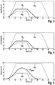
- an in Fig. 3 illustrated trapezoidal synchronization pulse P T is used with a predetermined edge steepness.
- the edge steepness lies between an edge steepness of a first Characteristic line representing a lower limit Vu and an edge sub-unit of a second characteristic line representing an upper limit Vo.
- EMC electromagnetic radiation
- a receiving device for receiving current signals comprises at least two bus connection devices for receiving current signals from several transmitters, each bus connection device being designed to be connected to at least one bus connection, and a control device for outputting synchronization pulses to the bus connection devices for synchronizing the transmitters.
- the bus connection devices output the synchronization pulses to the multiple transmitters with at least one time offset from one another, the synchronization pulses each having a trapezoidal shape with rounded corners.
- a transmission direction and a bus system for serial data transfer of binary data between at least two communication stations are known, which are coupled to one another via a single bus line.
- the transmitting device of a communication station has a circuit for setting the curve shape.
- a circuit for setting the curve shape generates an output signal from a data signal to be sent with signal edges that are as sinusoidal as possible.
- a transceiver circuit which receives data as a stepped sinusoidal signal wave over a twisted two-wire line.
- the receiving arrangement according to the invention for a control device in a vehicle with the features of independent claim 1 and the method according to the invention for generating a synchronization pulse with the features of independent claim 8 have the advantage that the sinusoidal configuration of the synchronization pulse within the specified limits means that it is as low as possible electromagnetic radiation, especially in the spectral range of signal transmission (100kHz to 300kHz), can be achieved.
- the core and advantage of the invention is not only to round off the corners of the synchronization pulse, but also to optimize the entire shape in such a way that that the electromagnetic radiation remains limited as far as possible to the range of the fundamental waves of the synchronization pulse.
- Embodiments of the present invention provide a receiving arrangement for a control device in a vehicle which has a voltage generator for generating a synchronization pulse which comprises a first voltage source, a current source and a current sink.
- the voltage generator generates the synchronization pulse within predetermined specification limits with a predetermined shape and a predetermined temporal behavior, and the receiving arrangement outputs the synchronization pulse to synchronize a signal transmission via a data bus to at least one sensor.
- the voltage generator generates the synchronization pulse via the current source and the current sink by charging and / or discharging a bus load, essentially as a sinusoidal oscillation.
- the current source can, for example, provide current values that are greater than or equal to 0 mA
- the current sink can, for example, provide current values that are less than 0 mA.
- a method for generating a synchronization pulse for synchronizing a subsequent signal transmission between a receiving arrangement and at least one sensor via a data bus in a vehicle is proposed.
- the synchronization pulse is generated within predetermined specification limits with a predetermined shape and a predetermined temporal behavior and is transmitted from the receiver arrangement to the at least one sensor.
- the synchronization pulse is generated essentially as a sinusoidal oscillation.
- the synchronization pulse can preferably be transmitted from the receiving arrangement to the at least one sensor before or at the beginning of the signal transmission between the at least one sensor and the receiver arrangement.
- the voltage generator comprises at least one digital control circuit and at least one digital-to-analog converter, which generate an essentially sinusoidal reference current and output it to the current source and the current sink.
- a first digital control circuit and a first digital-to-analog converter can generate an essentially sinusoidal reference current and output it to the current source.
- a second digital control circuit and a second digital-to-analog converter can also generate an essentially sinusoidal reference current and output it to the current sink.
- This advantageously enables a very robust implementation of the synchronization pulse and reduced electromagnetic radiation.
- the control of the synchronization pulse can be completely outsourced to the digital part of the circuit, which can lead to an area-efficient solution due to the increasingly advanced scaling of semiconductor technology.
- a voltage supply for the receiver can be decoupled from the data bus during the synchronization pulse, while the voltage generator for generating the synchronization pulse is activated. Since the voltage generator for generating the synchronization pulse comprises a current source and a current sink, there is no need for an additional switch in series with the current source and the current sink.
- a common digital control circuit and a common digital-to-analog converter can generate an essentially sinusoidal reference current and output it to the current source and the current sink.
- the form of the synchronization pulse can either be stored in the digital part or in the digital control circuit, or it can be calculated with the aid of an algorithm.
- the digital-to-analog converter generates a reference current from an N-bit data word, which is transferred to the data bus via the current source or current sink and the load on the data bus is charged or discharged.
- a substantially sinusoidal synchronization pulse ie a sinusoidal or an approximately sinusoidal synchronization pulse
- both the current source and the current sink are driven sinusoidally or approximately sinusoidally.
- the resolution of the data word can be selected in such a way that the synchronization pulse can be mapped without significant jumps.
- the capacity of the bus load integrates the bus current and in this way smooths the voltage on the data bus.
- the at least one digital control circuit can regulate the synchronization pulse based on the quiescent current and the bus load, the quiescent current regulation supplying a measure for the quiescent current and an achieved synchronization pulse amplitude providing a measure for the bus load.
- the synchronization pulse amplitude can be determined by evaluating the bus voltage.
- the information about the achieved synchronization pulse amplitude is obtained by evaluating the bus voltage.
- Knowledge of the quiescent current is necessary in order to ensure that the quiescent current is correctly taken over by the current sources of the voltage generator when the synchronization pulse starts.
- a decision threshold is defined and monitored within a defined time window, for example by a comparator.
- the at least one digital control circuit detects that the synchronization pulse amplitude is too high if the synchronization pulse reaches the decision threshold at a point in time which is before the time window.
- the at least one digital control circuit detects that the synchronization pulse amplitude is too low if the synchronization pulse does not reach the decision threshold during a period of the synchronization pulse.
- the at least one digital control circuit detects a correct synchronization pulse amplitude when the synchronization pulse reaches the decision threshold at a point in time which is within the time window.
- the evaluation of the synchronization pulse amplitude can be carried out at any point in the synchronization pulse, for example also along the rising or falling edge.
- the duration of the synchronization pulse is kept constant during the step heights of the reference current output by the digital-to-analog converter can be scaled according to the information from the amplitude evaluation.
- the step height can, for example, be calculated from the multiplication of the minimum possible step height by a scaling factor.
- the minimum step height results from the minimum current from the current source or current sink.
- the scaling factor is increased if the synchronization pulse is too low and reduced if the synchronization pulse is too high until the correct level is reached and the decision threshold is exceeded within the time window.
- the illustrated sensor arrangements 1, 1 ′ comprise a data bus 5, at least one sensor 7 and in each case an exemplary embodiment of a receiving arrangement 3, 3 ′ according to the invention for a control device in a vehicle.
- the receiving arrangements 3, 3 'according to the invention each comprise a voltage generator 30, 30' for generating a synchronization pulse P sync with a first voltage source 3.1, a current source 3.5 and a current sink 3.6.
- the voltage generator 30, 30 generates the synchronization pulse P sync via the current source 3.5 and the current sink 3.6 by charging and / or discharging a bus load essentially as a sinusoidal oscillation.
- the voltage generator 30, 30 'generates the synchronization pulse P sync within predetermined specification limits Vo, Vu with a predetermined shape and a predetermined temporal behavior.
- the receiving arrangement 3, 3 outputs the synchronization pulse P sync for synchronizing a subsequent signal transmission via a data bus 5 at least a sensor 7. So that a synchronous bus system with one sensor 7 or more sensors functions, the illustrated synchronization pulse P sync has a certain shape and a certain temporal behavior for all possible bus configurations and under all possible operating conditions. How out Fig.
- the synchronization pulse P sync has an edge steepness which is predetermined by the edge steepness of a first characteristic curve, which represents the lower limit Vu, and the edge steepness of a second characteristic curve, which represents the upper limit Vo. Due to the sine shape or the sine-like shape, the synchronization pulse P sync is optimized within the specified limits Vu, Vo in such a way that the lowest possible electromagnetic radiation can be achieved, especially in the spectral range of signal transmission (100kHz to 300kHz), which is based on the range of the fundamental waves Synchronization pulse P sync remains limited.
- the voltage generator 30, 30 comprises at least one digital control circuit 32, 42 and at least one digital-to-analog converter 34, 44, which generate an essentially sinusoidal reference current and output it to the current source 3.5 and the current sink 3.6.
- the exemplary embodiments shown enable a very robust implementation of the synchronization pulse P sync and reduced electromagnetic radiation.
- the control of the current source 3.5 and the current sink 3.6 for generating the synchronization pulse P sync can be completely outsourced to the digital part of the receiving arrangement 3, 3 ', which leads to an area-efficient solution due to the increasingly advanced scaling of semiconductor technology.
- a voltage supply 3.2 of the remaining circuits 3.3 of the receiving device 3, 'uncoupled during the generating and outputting of the synchronization pulse P sync via a switching unit 3.4 from the data bus 5, while the voltage generator 30, 30' 3 is activated to generate the synchronization pulse P sync becomes. Since the voltage generator 30, 30 'comprises the current source 3.5 and the current sink 3.6, there is no need for an additional switch in series with the current source 3.5 and the current sink 3.6.
- the illustrated first embodiment of the receiving arrangement 3 comprises a first voltage generator 30, which has a first digital control circuit 42 and a first digital-to-analog converter 44, which generate a substantially sinusoidal reference current and output it to the current source 3.5, and a second digital control circuit 32 and a second digital-to-analog converter 34, which generate a substantially sinusoidal reference current and output it to the current sink 3.6.
- the illustrated second exemplary embodiment of the receiving arrangement 3 ' comprises a second voltage generator 30', which comprises a common digital control circuit 32 and a common digital-to-analog converter 34, which generate a substantially sinusoidal reference current and are fed to the current source 3.5 and output the current sink 3.6.
- a second voltage generator 30' which comprises a common digital control circuit 32 and a common digital-to-analog converter 34, which generate a substantially sinusoidal reference current and are fed to the current source 3.5 and output the current sink 3.6.
- the number of components of the voltage generator 30 can be omitted Fig. 1 to reduce.
- the voltage generator 30 ' is omitted Fig. 1 compared to the voltage generator 30 Fig. 1 Layout area or silicon area.
- the form of the synchronization pulse P sync is either stored in the digital part or in the digital control circuit 32, 42 or is calculated in the digital part or in the digital control circuit 32, 42 with the aid of an algorithm.
- At least one digital-to-analog converter 34, 44 generates a reference current from the N-bit data word, which is conducted to the data bus via the current source 3.5 or current sink 3.6 and charges or discharges the load on the data bus.
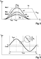
- Fig. 5 To get a sinusoidal or approximately sinusoidal synchronization pulse P sync
- both the current source 3.5 and the current sink 3.6 are driven sinusoidally or approximately sinusoidally.
- Figures 6 and 7 sketch the basic sequence control for generating the synchronization pulse P sync, where Fig.
- Fig. 7 shows a corresponding current pulse I sync .
- the current source 3.5 provides a quiescent current I 0 from the voltage supply 3.2 of the receiving arrangement 3, 3 '.
- the information about the quiescent current I 0 receives the current source 3.5 from a known from the prior art Quiescent current readjustment.
- the greatest current I sync flows from the current source 3.5 and at the maximum Max of the voltage pulse U sync , only the quiescent current I 0 flows from the current source 3.5.
- the current I sync is reduced by the current source 3.5 until it finally becomes zero and the current sink 3.6 starts a discharge process.
- the largest current I sync flows into the current sink 3.6 and then decreases again until the current source 3.5 intervenes again and delivers the current I sync in the last phase of the synchronization pulse P sync up to the end time t 2.
- the quiescent current is again taken over from the voltage supply 3.2 of the receiving arrangement 3, 3 '.
- the resolution of the data word is selected so that the synchronization pulse P sync can be mapped without significant jumps.
- the capacity of the bus load integrates the bus current I Bus and in this way smoothes the voltage U Bus on the data bus 5.
- the bus load can vary greatly depending on the bus operation and requires a certain driver capability of the current source 3.5 and the current sink 3.6. This means that the current source 3.5 and the current sink 3.6 are capable of providing or receiving a sufficiently high current to enable the desired shape of the synchronization pulse P sync without signal dips and signal deformations. This driver capability is an important influencing variable when choosing an appropriate resolution of the digital-to-analog converter 34, 44.
- Fig. 5 As can be seen, requirements are placed on the shape and edge steepness of the synchronization pulse P sync.
- the edge steepness must not be too low, since this results in higher tolerances in the detection time of the sensors 7. This in turn can limit the maximum number of sensors 7 and thus reduce the data throughput.
- the edge steepness must not be too high, as this leads to increased electromagnetic radiation.
- Two variables that strongly influence the behavior of the synchronization pulse P sync are the bus load and the quiescent current I 0 des Sensor 7 or the sensors. Different bus and sensor configurations have very different loads and quiescent currents I 0 . In order to be able to represent a synchronization pulse P sync within the specified limits Vu, Vo despite these strong bus load and quiescent current variations, the bus current I bus or the bus voltage U bus is regulated.
- the digital control circuit 32, 42 uses the information about the quiescent current I 0 from the quiescent current readjustment and the information about the achieved synchronization pulse amplitude Max to control the synchronization pulse P sync. Knowing the quiescent current I 0 is necessary at the start of the synchronization pulse P sync a correct implementation of the quiescent current to ensure I 0 by the power source voltage of 3.5 sync pulse generator.
- the voltage generator 30, 30 ' which generates the synchronization pulse P sync and the at least one digital control 32, 42, the at least one digital-to-analog converter 34, 44, the current source 3.5, the current sink 3.6 and the voltage supply 3.1 is referred to as the synchronization pulse generator for the power source 3.5 includes.
- the synchronization pulse amplitude Max is determined by evaluating the bus voltage U Bus. To evaluate the bus voltage U bus, a decision threshold U reg and a time window ⁇ t reg are defined. The at least one digital control circuit 32, 42 detects an excessively high synchronization pulse amplitude Max1 when the synchronization pulse P sync reaches the decision threshold U reg at a point in time t reg1 which is before the time window ⁇ t reg . This state is in Fig. 8 represented by a first characteristic curve K1. The at least one digital control circuit 32, recognizes 42 does not reach a too low synchronization pulse amplitude Max2 when the synchronization pulse P sync the decision threshold U reg during a period of time t sync the synchronization pulse P sync.
- This state is in Fig. 8 represented by a second characteristic curve K2.
- the at least one digital control circuit 32, 42 detects a correct synchronization pulse amplitude Max when the synchronization pulse P sync reaches the decision threshold U reg at a point in time t reg2 which is within the time window ⁇ t reg .
- This state is in Fig. 8 represented by a third characteristic curve K3.
- the decision threshold U reg can be monitored by a comparator, for example. If the decision threshold U reg is exceeded too early, ie before the monitoring window ⁇ t reg , then an excessively high synchronization pulse P sync was generated. If the decision threshold U reg is never exceeded, then a too low synchronization pulse P sync generated.
- a synchronization pulse P sync with a correct level Only when the decision threshold U reg has been exceeded in the monitored time window ⁇ t reg is a synchronization pulse P sync with a correct level.
- the evaluation of the synchronization pulse amplitude can be carried out at any point in the synchronization pulse P sync, for example also along the rising or falling edge.
- the lowest tolerances and thus the most reliable regulation are to be expected in the vicinity of the maximum of the pulse voltage U sync , since the voltage is subject to the smallest changes here.
- the duration of the synchronization pulse t sync is kept constant, while the step height S h of the output current pulse I sync based on the at least one digital-to-analog converter 34, 44 can be scaled according to the information from the amplitude evaluation.
- the step height S h is calculated from the multiplication of the minimum possible step height by a scaling factor.
- the minimum step height results from the minimum output current value of the current source 3.5 or current sink 3.6.
- the scaling factor is increased at too low a synchronization pulse P sync and reduced at too high a synchronization pulse P sync, until the correct height is reached and the decision threshold U reg within the time window is exceeded .DELTA.t reg.
- Embodiments of the method according to the invention for generating a synchronization pulse P sync for synchronizing a subsequent signal transmission between the receiving arrangement 3, 3 'and at least one sensor 7 via a data bus 5 in a vehicle generate the synchronization pulse P sync within predetermined specification limits Vo, Vu with a predetermined shape and a predetermined behavior over time.
- the synchronization pulse P sync is transmitted from the receiver arrangement 3, 3 ′ to the at least one sensor 7.
- the synchronization pulse P sync is generated essentially as a sinusoidal oscillation.
Landscapes
- Engineering & Computer Science (AREA)
- Computer Networks & Wireless Communication (AREA)
- Signal Processing (AREA)
- Physics & Mathematics (AREA)
- Spectroscopy & Molecular Physics (AREA)
- Power Engineering (AREA)
- Mechanical Engineering (AREA)
- Dc Digital Transmission (AREA)
- Analogue/Digital Conversion (AREA)
- Cable Transmission Systems, Equalization Of Radio And Reduction Of Echo (AREA)
- Arrangements For Transmission Of Measured Signals (AREA)
Description
- Die Erfindung geht aus von einer Empfangsanordnung für ein Steuergerät in einem Fahrzeug nach der Gattung des unabhängigen Patentanspruchs 1 und von einem zugehörigen Verfahren zum Erzeugen eines Synchronisationspulses nach der Gattung des unabhängigen Patentanspruchs 8.
- Zur Übertragung von Sensordaten an ein zentrales Steuergerät (ECU) in einem Fahrzeug nutzen periphere Sensoren für Insassenschutzsysteme meist Stromschnittstellen (z.B. PAS4, PSI5). Bei Stromschnittstellen der neuesten Generation (PSI5) wird mittels Synchronisierung der Busbetrieb mit mehreren Sensoren an einem Empfänger ermöglicht. Für die Funktion der Synchronisierung wird vom zentralen Steuergerät (ECU) ein Arbeitstakt in Form eines Spannungspulses erzeugt, welcher von den Sensoren am Bus detektiert wird und den Beginn eines neuen Zyklus für die Datenübertragung kennzeichnet. Dieser Spannungspuls wird als Synchronisationspuls bezeichnet und entsteht mit Hilfe von Stromquellen und Stromsenken, welche die Buslast auf- bzw. entladen. Typischerweise wird dieser Spannungspuls alle 500 µs wiederholt.
- Damit ein synchrones Bussystem mit einem Sensor oder mehreren Sensoren funktioniert, ist es wichtig, dass der Synchronisationspuls für alle möglichen Buskonfigurationen und unter allen möglichen Betriebsbedingungen eine bestimmte Form und ein bestimmtes zeitliches Verhalten aufweist. Daher wird bei bekannten synchronen Bussystemen in der Regel ein in
Fig. 3 dargestellter trapezförmiger Synchronisationspuls PT mit einer vorgegebenen Flankensteilheit verwendet. Hierbei liegt die Flankensteilheit zwischen einer Flankensteilheit einer ersten Kennlinie, welche eine untere Grenze Vu repräsentiert, und einer Flankensteileinheit einer zweiten Kennlinie, welche eine obere Grenze Vo repräsentiert. Während des synchronen Busbetriebs führt die Trapezform des Synchronisationspulses PT durch den hohen Oberwellenanteil zu verstärkter elektromagnetischer Abstrahlung (EMV) im Frequenzspektrum der Signalübertragung. Dem kann in gewissem Maße beispielsweise durch einen inFig. 4 dargestellten Synchronisationspuls PTr entgegengewirkt werden, welcher eine Trapezform mit vier abgerundeten Ecken aufweist. - In der Offenlegungsschrift
DE 10 2009 001 370 A1 werden eine Empfangseinrichtung zum Aufnehmen von Stromsignalen, eine Schaltungsanordnung mit einer solchen Empfangseinrichtung und ein Verfahren zum Übertragen von Stromsignalen über ein Bussystem beschrieben. Die beschriebene Empfangseinrichtung umfasst zum Aufnehmen von Stromsignalen mehrerer Sender mindestens zwei Busanschlusseinrichtungen, wobei jede Busanschlusseinrichtung zum Anschluss an jeweils mindestens eine Busverbindung ausgebildet ist, und eine Steuereinrichtung zur Ausgabe von Synchronisationspulsen an die Busanschlusseinrichtungen zur Synchronisierung der Sender. Die Busanschlusseinrichtungen geben die Synchronisationspulse mit mindestens einem Zeitversatz zueinander an die mehreren Sender aus, wobei die Synchronisationspulse jeweils eine Trapezform mit abgerundeten Ecken ausweisen. - Aus der
EP 0 959 595 A2 ist eine Sendeenrichtung und ein Bussystem zum seriellen Datentransfer von binären Daten zwischen mindestens zwei Kommunikationsstationen bekannt, die über eine einzelne Busleitung miteinander gekoppelt sind. Die Sendeeinrichtung einer Kommunikationsstation weist eine Schaltung zur Kurvenformeinstellung auf. Schaltung zur Kurvenformeinstellung erzeugt aus einem zu sendenden Datensignal ein Ausgangssignal mit möglichst sinushalbwellenförmigen Signalflanken. - Aus der
US 5,408,497 ist eine Transceiverschaltung bekannt, welche Daten als stufige sinusförmige Signalwelle über eine verdrillte Zweidrahtleitung empfängt. - Die erfindungsgemäße Empfangsanordnung für ein Steuergerät in einem Fahrzeug mit den Merkmalen des unabhängigen Patentanspruchs 1 und das erfindungsgemäße Verfahren zum Erzeugen eines Synchronisationspulses mit den Merkmalen des unabhängigen Patentanspruchs 8 haben demgegenüber den Vorteil, dass durch die sinusförmige Ausbildung des Synchronisationspulses in den vorgegebenen Grenzen eine möglichst geringe elektromagnetische Abstrahlung, insbesondere im Spektralbereich der Signalübertragung (100kHz bis 300kHz), erreicht werden kann.
- Der Kern und Vorteil der Erfindung besteht darin, nicht nur die Ecken des Synchronisationspulses abzurunden, sondern die ganze Form derart zu optimieren, dass die elektromagnetische Abstrahlung möglichst auf den Bereich der Grundwellen des Synchronisationspulses beschränkt bleibt.
- Ausführungsformen der vorliegenden Erfindung stellen eine Empfangsanordnung für ein Steuergerät in einem Fahrzeug zur Verfügung, welche einen Spannungsgenerator zur Erzeugung eines Synchronisationspulses aufweist, welcher eine erste Spannungsquelle, eine Stromquelle und eine Stromsenke umfasst. Der Spannungsgenerator erzeugt den Synchronisationspuls innerhalb von vorgegebenen Spezifikationsgrenzen mit einer vorgegebenen Form und einem vorgegebenen zeitlichen Verhalten, und die Empfangsanordnung gibt den Synchronisationspuls zur Synchronisierung einer Signalübertragung über einen Datenbus an mindestens einen Sensor aus. Erfindungsgemäß erzeugt der Spannungsgenerator den Synchronisationspuls über die Stromquelle und die Stromsenke durch Aufladen und/oder Entladen einer Buslast im Wesentlichen als Sinusschwingung. Hierbei kann die Stromquelle beispielsweise Stromwerte bereitstellen, welche größer oder gleich 0mA sind, und die Stromsenke kann beispielsweise Stromwerte bereitstellen, welche kleiner als 0mA sind.
- Zudem wird ein Verfahren zum Erzeugen eines Synchronisationspulses zur Synchronisierung einer nachfolgenden Signalübertragung zwischen einer Empfangsanordnung und mindestens einem Sensor über einen Datenbus in einem Fahrzeug vorgeschlagen. Der Synchronisationspuls wird innerhalb von vorgegebenen Spezifikationsgrenzen mit einer vorgegebenen Form und einem vorgegebenen zeitlichen Verhalten erzeugt und von der Empfängeranordnung an den mindestens einen Sensor übertragen. Erfindungsgemäß wird der Synchronisationspuls im Wesentlichen als Sinusschwingung erzeugt.
- Der Synchronisationspuls kann vorzugsweise vor bzw. zu Beginn der Signalübertragung zwischen dem mindestens einen Sensor und der Empfängeranordnung von der Empfangsanordnung an den mindestens einen Sensor übertragen werden.
- Durch die in den abhängigen Ansprüchen aufgeführten Maßnahmen und Weiterbildungen sind vorteilhafte Verbesserungen der im unabhängigen Patentanspruch 1 angegebenen Empfangsanordnung für ein Steuergerät in einem Fahrzeug möglich.
- Gemäss der Erfindung umfasst der Spannungsgenerator mindestens eine digitale Ansteuerschaltung und mindestens einen Digital-Analog-Wandler umfasst, welche einen im Wesentlichen sinusförmigen Referenzstrom erzeugen und an die Stromquelle und die Stromsenke ausgeben.
- In vorteilhafter Ausgestaltung der erfindungsgemäßen Empfangsanordnung können eine erste digitale Ansteuerschaltung und ein erster Digital-Analog-Wandler einen im Wesentlichen sinusförmigen Referenzstrom erzeugen und an die Stromquelle ausgeben. Eine zweite digitale Ansteuerschaltung und ein zweiter Digital-Analog-Wandler können ebenfalls einen im Wesentlichen sinusförmigen Referenzstrom erzeugen und an die Stromsenke ausgeben. Dies ermöglicht in vorteilhafter Weise eine sehr robuste Realisierung des Synchronisationspulses und eine reduzierte elektromagnetische Abstrahlung. Hinzu kommt, dass die Ansteuerung des Synchronisationspulses vollständig in den Digitalteil der Schaltung ausgelagert werden kann, was aufgrund der immer fortschrittlicheren Skalierung der Halbleitertechnologie zu einer flächeneffizienten Lösung führen kann. Eine Spannungsversorgung des Empfängers kann während des Synchronisationspulses vom Datenbus abgekoppelt werden, während der Spannungsgenerator zur Erzeugung des Synchronisationspulses aktiviert wird. Da der Spannungsgenerator zur Erzeugung des Synchronisationspulses eine Stromquelle und eine Stromsenke umfasst, kann die Notwendigkeit für einen zusätzlichen Schalter in Serie mit der Stromquelle und der Stromsenke entfallen.
- In weiterer vorteilhafter Ausgestaltung der erfindungsgemäßen Empfangsanordnung können eine gemeinsame digitale Ansteuerschaltung und ein gemeinsamer Digital-Analog-Wandler einen im Wesentlichen sinusförmigen Referenzstrom erzeugen und an die Stromquelle und die Stromsenke ausgeben. Durch eine gemeinsame Nutzung der digitalen Ansteuerschaltung und des Digital-Analog-Wandlers kann die Anzahl der Bauteile des Spannungsgenerators reduziert und Layoutfläche eingespart werden.
- Die Form des Synchronisationspulses kann entweder im Digitalteil bzw. in der digitalen Ansteuerschaltung hinterlegt oder mit Hilfe eines Algorithmus berechnet werden. Der Digital-Analog-Wandler erzeugt aus einem N-Bit Datenwort einen Referenzstrom, welcher über die Stromquelle bzw. Stromsenke auf den Datenbus geleitet wird und die am Datenbus anliegende Last auflädt bzw. entlädt. Um einen im Wesentlichen sinusförmigen Synchronisationspuls, d.h. einen sinusförmigen oder einen annähernd sinusförmigen Synchronisationspuls, zu erzeugen, wird sowohl die Stromquelle als auch die Stromsenke sinusförmig oder annähernd sinusförmig angesteuert. Die Auflösung des Datenworts kann aus Abstrahlgründen derart gewählt werden, dass der Synchronisationspuls ohne signifikante Sprünge abgebildet werden kann. Die Kapazität der Buslast integriert den Busstrom und glättet auf diese Weise die Spannung auf dem Datenbus.
- Die erfindungsgemässe Empfangsanordnung kann die mindestens eine digitale Ansteuerschaltung den Synchronisationspuls basierend auf dem Ruhestrom und der Buslast regeln, wobei die Ruhestromregelung ein Maß für den Ruhestrom und eine erreichte Synchronisationspulsamplitude ein Maß für die Buslast liefert. Die Synchronisationspulsamplitude kann durch eine Bewertung der Busspannung ermittelt werden. Die Information über die erreichte Synchronisationspulsamplitude wird über die Bewertung der Busspannung gewonnen. Die Kenntnis des Ruhestroms ist erforderlich, um beim Start des Synchronisationspulses eine korrekte Übernahme des Ruhestroms durch die Stromquellen des Spannungsgenerators zu gewährleisten. Zur Bewertung der Busspannung wird eine Entscheidungsschwelle definiert und innerhalb eines definierten Zeitfensters, beispielsweise von einem Komparator überwacht. Die mindestens eine digitale Ansteuerschaltung erkennt eine zu hohe Synchronisationspulsamplitude, wenn der Synchronisationspuls die Entscheidungsschwelle zu einem Zeitpunkt erreicht, welcher vor dem Zeitfenster liegt. Die mindestens eine digitale Ansteuerschaltung erkennt eine zu niedrige Synchronisationspulsamplitude, wenn der Synchronisationspuls die Entscheidungsschwelle während einer Periodendauer des Synchronisationspulses nicht erreicht. Die mindestens eine digitale Ansteuerschaltung erkennt eine korrekte Synchronisationspulsamplitude, wenn der Synchronisationspuls die Entscheidungsschwelle zu einem Zeitpunkt erreicht, welcher innerhalb des Zeitfensters liegt. Prinzipiell lässt sich die Bewertung der Synchronisationspulsamplitude an einer beliebigen Stelle des Synchronisationspulses durchführen, beispielsweise auch entlang der steigenden oder fallenden Flanke. Allerdings sind die geringsten Toleranzen und damit die zuverlässigste Regelung in der Umgebung des Maximums der Pulsspannung zu erwarten, da die Spannung hier den kleinsten Änderungen unterliegt. Die Dauer des Synchronisationspulses wird konstant gehalten, während die Stufenhöhen des vom Digital-Analog-Wandler ausgegebenen Referenzstromes entsprechend der Information aus der Amplitudenbewertung skaliert werden können. Die Stufenhöhe kann beispielsweise aus der Multiplikation der minimal möglichen Stufenhöhe mit einem Skalierungsfaktor berechnet werden. Die minimale Stufenhöhe ergibt sich aus dem minimalen Strom aus der Stromquelle bzw. Stromsenke. Der Skalierungsfaktor wird bei einem zu niedrigen Synchronisationspuls vergrößert und bei einem zu hohen Synchronisationspuls verkleinert, bis die richtige Höhe erreicht wird und die Entscheidungsschwelle innerhalb des Zeitfensters überschritten wird.
- Ausführungsbeispiele der Erfindung sind in den Zeichnungen dargestellt und werden in der nachfolgenden Beschreibung näher erläutert. In den Zeichnungen bezeichnen gleiche Bezugszeichen Komponenten bzw. Elemente, die gleiche bzw. analoge Funktionen ausführen.
-
-
Fig. 1 zeigt ein schematisches Blockdiagramm einer Sensoranordnung mit einem ersten Ausführungsbeispiel einer erfindungsgemäßen Empfängeranordnung für ein Steuergerät in einem Fahrzeug, welche einen optimierten Synchronisationspuls erzeugt und ausgibt. -
Fig. 2 zeigt ein schematisches Blockdiagramm einer Sensoranordnung mit einem zweiten Ausführungsbeispiel einer erfindungsgemäßen Empfängeranordnung für ein Steuergerät in einem Fahrzeug, welche einen optimierten Synchronisationspuls erzeugt und ausgibt. -
Fig. 3 zeigt eine schematische Darstellung der Form und des zeitlichen Verhaltens eines herkömmlichen trapezförmigen Synchronisationspulses innerhalb von vorgegebenen Grenzen. -
Fig. 4 zeigt eine schematische Darstellung der Form und des zeitlichen Verhaltens eines herkömmlichen abgerundeten trapezförmigen Synchronisationspulses innerhalb der vorgegebenen Grenzen. -
Fig. 5 zeigt eine schematische Darstellung der Form und des zeitlichen Verhaltens eines erfindungsgemäß optimierten Synchronisationspulses innerhalb der vorgegebenen Grenzen. -
Fig. 6 zeigt eine schematische Darstellung der Busspannung während eines erfindungsgemäß optimierten Synchronisationspulses. -
Fig. 7 zeigt eine erste schematische Darstellung des Busstroms während eines erfindungsgemäß optimierten Synchronisationspulses. -
Fig. 8 zeigt eine schematische Darstellung des Prinzips der Regelung der Synchronisationspulsamplitude mit drei Synchronisationspulsen mit unterschiedlichen Amplituden, von denen nur die mittlere Kurve innerhalb der spezifizierten Grenzen liegt. -
Fig. 9 zeigt eine zweite schematische Darstellung des Busstroms während eines erfindungsgemäß optimierten Synchronisationspulses. - Wie aus
Fig. 1 und 2 ersichtlich ist, umfassen die dargestellten Sensoranordnungen 1,1' einen Datenbus 5, mindestens einen Sensor 7 und jeweils ein Ausführungsbeispiel einer erfindungsgemäßen Empfangsanordnung 3, 3' für ein Steuergerät in einem Fahrzeug. Die erfindungsgemäßen Empfangsanordnungen 3, 3' umfassen jeweils einen Spannungsgenerator 30, 30' zur Erzeugung eines Synchronisationspulses Psync mit einer ersten Spannungsquelle 3.1, einer Stromquelle 3.5 und einer Stromsenke 3.6. Erfindungsgemäß erzeugt der Spannungsgenerator 30, 30' den Synchronisationspuls Psync über die Stromquelle 3.5 und die Stromsenke 3.6 durch Aufladen und/oder Entladen einer Buslast im Wesentlichen als Sinusschwingung. - Wie aus
Fig. 5 ersichtlich ist, erzeugt der Spannungsgenerator 30, 30' den Synchronisationspuls Psync innerhalb von vorgegebenen Spezifikationsgrenzen Vo, Vu mit einer vorgegebenen Form und einem vorgegebenen zeitlichen Verhalten. Die Empfangsanordnung 3, 3' gibt den Synchronisationspuls Psync zur Synchronisierung einer nachfolgenden Signalübertragung über einen Datenbus 5 an mindestens einen Sensor 7 aus. Damit ein synchrones Bussystem mit einem Sensor 7 oder mehreren Sensoren funktioniert, weist der dargestellte Synchronisationspuls Psync für alle möglichen Buskonfigurationen und unter allen möglichen Betriebsbedingungen eine bestimmte Form und ein bestimmtes zeitliches Verhalten auf. Wie ausFig. 5 weiter ersichtlich ist, weist der Synchronisationspuls Psync eine Flankensteilheit auf, welche durch die Flankensteilheit einer ersten Kennlinie, welche die untere Grenze Vu repräsentiert, und die Flankensteilheit einer zweiten Kennlinie, welche die obere Grenze Vo repräsentiert, vorgegeben wird. Durch die Sinusform oder die sinusähnliche Form ist der Synchronisationspuls Psync in den vorgegebenen Grenzen Vu, Vo derart optimiert, dass eine möglichst geringe elektromagnetische Abstrahlung, insbesondere im Spektralbereich der Signalübertragung (100kHz bis 300kHz) erreicht werden kann, welche auf den Bereich der Grundwellen des Synchronisationspulses Psync beschränkt bleibt. - Wie aus
Fig. 1 und 2 weiter ersichtlich ist, umfasst der Spannungsgenerator 30, 30' mindestens eine digitale Ansteuerschaltung 32, 42 und mindestens einen Digital-Analog-Wandler 34, 44, welche einen im Wesentlichen sinusförmigen Referenzstrom erzeugen und an die Stromquelle 3.5 und die Stromsenke 3.6 ausgeben. Die dargestellten Ausführungsbeispiele ermöglichen eine sehr robuste Realisierung des Synchronisationspulses Psync und eine reduzierte elektromagnetischen Abstrahlung. Zudem kann die Ansteuerung der Stromquelle 3.5 und der Stromsenke 3.6 zur Erzeugung des Synchronisationspulses Psync vollständig in den Digitalteil der Empfangsanordnung 3, 3' ausgelagert werden, was aufgrund der immer fortschrittlicheren Skalierung der Halbleitertechnologie zu einer flächeneffizienten Lösung führt. - Wie aus
Fig. 1 und 2 weiter ersichtlich ist, wird eine Spannungsversorgung 3.2 der restlichen Schaltkreise 3.3 der Empfangsanordnung 3, 3' während der Erzeugung und Ausgabe des Synchronisationspulses Psync über eine Schalteinheit 3.4 vom Datenbus 5 abgekoppelt, während der Spannungsgenerator 30, 30' zur Erzeugung des Synchronisationspulses Psync aktiviert wird. Da der Spannungsgenerator 30, 30' die Stromquelle 3.5 und die Stromsenke 3.6 umfasst, entfällt die Notwendigkeit für einen zusätzlichen Schalter in Serie mit der Stromquelle 3.5 und der Stromsenke 3.6. - Wie aus
Fig. 1 weiter ersichtlich ist, umfasst das dargestellte erste Ausführungsbeispiel der erfindungsgemäßen Empfangsanordnung 3 einen ersten Spannungsgenerator 30, welcher eine erste digitale Ansteuerschaltung 42 und einen ersten Digital-Analog-Wandler 44, welche einen im Wesentlichen sinusförmigen Referenzstrom erzeugen und an die Stromquelle 3.5 ausgeben, und eine zweite digitale Ansteuerschaltung 32 und einen zweiten Digital-Analog-Wandler 34 umfasst, welche einen im Wesentlichen sinusförmigen Referenzstrom erzeugen und an die Stromsenke 3.6 ausgeben. - Wie aus
Fig. 2 weiter ersichtlich ist, umfasst das dargestellte zweite Ausführungsbeispiel der erfindungsgemäßen Empfangsanordnung 3' einen zweiten Spannungsgenerator 30', welcher eine gemeinsame digitale Ansteuerschaltung 32 und einen gemeinsamen Digital-Analog-Wandler 34 umfasst, welche einen im Wesentlichen sinusförmigen Referenzstrom erzeugen und an die Stromquelle 3.5 und die Stromsenke 3.6 ausgeben. Durch die gemeinsame Nutzung der digitalen Ansteuerschaltung 32 und des Digital-Analog-Wandlers 34 für die Stromquelle 3.5 und die Stromsenke 3.6 lässt sich die Anzahl der Bauelemente des Spannungsgenerators 30 ausFig. 1 reduzieren. Dadurch spart der Spannungsgenerator 30' ausFig. 1 im Vergleich zum Spannungsgenerator 30 ausFig. 1 Layoutfläche bzw. Siliziumfläche ein. - Die Form des Synchronisationspulses Psync ist entweder im Digitalteil bzw. in der digitalen Ansteuerschaltung 32, 42 hinterlegt oder wird im Digitalteil bzw. in der digitalen Ansteuerschaltung 32, 42 mit Hilfe eines Algorithmus berechnet. Mindestens ein Digital-Analog-Wandler 34, 44 erzeugt aus dem N-Bit Datenwort einen Referenzstrom, welcher über die Stromquelle 3.5 bzw. Stromsenke 3.6 auf den Datenbus geleitet wird und die am Datenbus anliegende Last auf- bzw. entlädt. Um einen sinusförmigen oder annähernd sinusförmigen Synchronisationspuls Psync aus
Fig. 5 zu erzeugen, werden sowohl die Stromquelle 3.5 als auch die Stromsenke 3.6 sinusförmig oder annähernd sinusförmig angesteuert.Fig. 6 und 7 skizzieren die prinzipielle Ablaufsteuerung zur Erzeugung des Synchronisationspulses Psync, wobeiFig. 6 einen Spannungspuls Usync undFig. 7 einen korrespondierenden Strompuls Isync zeigt. Im Startpunkt t1 des Synchronisationspulses Psync stellt die Stromquelle 3.5 einen Ruhestrom I0 aus der Spannungsversorgung 3.2 der Empfangsanordnung 3, 3' bereit. Die Information über den Ruhestrom I0 erhält die Stromquelle 3.5 aus einer aus dem Stand der Technik bekannten Ruhestromnachregelung. Im ersten Wendepunkt des Spannungspulses Usync fließt der größte Strom Isync aus der Stromquelle 3.5 und im Maximum Max des Spannungspulses Usync fließt wiederum lediglich der Ruhestrom I0 aus der Stromquelle 3.5. Um die fallende Flanke des Synchronisationspulses Psync zu implementieren, wird nach Erreichen des Spannungsmaximums Max der Strom Isync durch die Stromquelle 3.5 reduziert, bis er schließlich zu Null wird und die Stromsenke 3.6 einen Entladevorgang startet. Im zweiten Wendepunkt des Spannungspulses Usync fließt dann der größte Strom Isync in die Stromsenke 3.6 und nimmt dann wieder ab, bis erneut die Stromquelle 3.5 eingreift und in der letzten Phase des Synchronisationspulses Psync bis zum Endzeitpunkt t2 den Strom Isync liefert. Zum Endzeitpunkt t2 wird der Ruhestrom wiederum aus der Spannungsversorgung 3.2 der Empfangsanordnung 3, 3' übernommen. Somit stellt die Stromquelle 3.5 während der Dauer tsync des Synchronisationspulses Psync Stromwerte bereit, welche größer oder gleich 0mA sind, und die Stromsenke 3.6 stellt Stromwerte bereit, welche kleiner als 0mA sind. - Die Auflösung des Datenworts ist aus Abstrahlgründen so gewählt, dass der Synchronisationspuls Psync ohne signifikante Sprünge abgebildet werden kann. Die Kapazität der Buslast integriert den Busstrom IBus und glättet auf diese Weise die Spannung UBus auf dem Datenbus 5. Die Buslast kann abhängig vom Busbetrieb stark variieren und macht eine gewisse Treiberfähigkeit der Stromquelle 3.5 und der Stromsenke 3.6 erforderlich. Das bedeutet, dass die Stromquelle 3.5 und die Stromsenke 3.6 in der Lage sind, einen ausreichend hohen Strom bereitzustellen bzw. aufzunehmen, um die gewünschte Form des Synchronisationspulses Psync ohne Signaleinbrüche und Signalverformungen zu ermöglichen. Diese Treiberfähigkeit ist eine wichtige Einflussgröße bei der Wahl einer angemessenen Auflösung des Digital-Analog-Wandlers 34, 44.
- Wie aus
Fig. 5 ersichtlich ist, werden Anforderungen an die Form und Flankensteilheit des Synchronisationspulses Psync gestellt. Zum einen darf die Flankensteilheit nicht zu gering sein, da dies höhere Toleranzen der Erkennungszeit der Sensoren 7 zur Folge hat. Dies wiederum kann die maximale Anzahl an Sensoren 7 beschränken und somit den Datendurchsatz reduzieren. Zum anderen darf die Flankensteilheit nicht zu hoch sein, da dies zu verstärkter elektromagnetischer Abstrahlung führt. Zwei Größen, welche das Verhalten des Synchronisationspulses Psync stark beeinflussen, sind die Buslast und der Ruhestrom I0 des Sensors 7 bzw. der Sensoren. Verschiedene Bus- und Sensorkonfigurationen weisen stark unterschiedliche Lasten und Ruheströme I0 auf. Um trotz dieser starken Buslast- und Ruhestromvariationen einen Synchronisationspuls Psync innerhalb der vorgegebenen Grenzen Vu, Vo darstellen zu können, wird eine Regelung des Busstroms IBus bzw. der Busspannung UBus durchgeführt. - Die digitale Ansteuerschaltung 32, 42 verwendet die Information über den Ruhestrom I0 aus der Ruhestromnachregelung und die Information über die erreichte Synchronisationspulsamplitude Max zur Regelung des Synchronisationspulses Psync. Die Kenntnis des Ruhestroms I0 ist notwendig, um beim Start des Synchronisationspulses Psync eine korrekte Übernahme des Ruhestroms I0 durch die Stromquelle 3.5 des Spannungssynchronisationspulsgenerators zu gewährleisten. Als Synchronisationspulsgenerator wird der Spannungsgenerator 30, 30' bezeichnet, welcher den Synchronisationspuls Psync erzeugt und die mindestens eine digitale Ansteuerung 32, 42, den mindestens einen Digital-Analog-Wandler 34, 44, die Stromquelle 3.5, die Stromsenke 3.6 und die Spannungsversorgung 3.1 für die Stromquelle 3.5 umfasst. Die Synchronisationspulsamplitude Max wird durch die Bewertung der Busspannung UBus ermittelt. Zur Bewertung der Busspannung UBus werden eine Entscheidungsschwelle Ureg und ein Zeitfenster Δtreg definiert. Die mindestens eine digitale Ansteuerschaltung 32, 42 erkennt eine zu hohe Synchronisationspulsamplitude Max1, wenn der Synchronisationspuls Psync die Entscheidungsschwelle Ureg zu einem Zeitpunkt treg1 erreicht, welcher vor dem Zeitfenster Δtreg liegt. Dieser Zustand wird in
Fig. 8 durch eine erste Kennlinie K1 repräsentiert. Die mindestens eine digitale Ansteuerschaltung 32, 42 erkennt eine zu niedrige Synchronisationspulsamplitude Max2, wenn der Synchronisationspuls Psync die Entscheidungsschwelle Ureg während einer Periodendauer tsync des Synchronisationspulses Psync nicht erreicht. Dieser Zustand wird inFig. 8 durch eine zweite Kennlinie K2 repräsentiert. Die mindestens eine digitale Ansteuerschaltung 32, 42 erkennt eine korrekte Synchronisationspulsamplitude Max, wenn der Synchronisationspuls Psync die Entscheidungsschwelle Ureg zu einem Zeitpunkt treg2 erreicht, welcher innerhalb des Zeitfensters Δtreg liegt. Dieser Zustand wird inFig. 8 durch eine dritte Kennlinie K3 repräsentiert. Die Entscheidungsschwelle Ureg kann beispielsweise von einem Komparator überwacht werden. Wird die Entscheidungsschwelle Ureg zu früh, d.h. vor dem Überwachungsfenster Δtreg, überschritten, dann wurde ein zu hoher Synchronisationspuls Psync erzeugt. Wird die Entscheidungsschwelle Ureg nie überschritten, dann wurde ein zu niedriger Synchronisationspuls Psync erzeugt. Erst wenn die Entscheidungsschwelle Ureg im überwachten Zeitfenster Δtreg überschritten wurde, liegt ein Synchronisationspuls Psync mit einer korrekten Höhe vor. Prinzipiell lässt sich die Bewertung der Synchronisationspulsamplitude an einer beliebigen Stelle des Synchronisationspulses Psync durchführen, beispielsweise auch entlang der ansteigenden oder abfallenden Flanke. Allerdings sind die geringsten Toleranzen und damit die zuverlässigste Regelung in der Umgebung des Maximums der Pulsspannung Usync zu erwarten, da die Spannung hier den kleinsten Änderungen unterliegt. - Wie aus
Fig. 9 ersichtlich ist, wird die Dauer des Synchronisationspulses tsync konstant gehalten, während die auf dem mindestens einen Digital-Analog-Wandler 34, 44 basierende Stufenhöhe Sh des ausgegebenen Strompulses Isync entsprechend der Information aus der Amplitudenbewertung skaliert werden kann. Die Stufenhöhe Sh wird aus der Multiplikation der minimal möglichen Stufenhöhe mit einem Skalierungsfaktor berechnet. Die minimale Stufenhöhe ergibt sich aus dem minimalen ausgebbaren Stromwert der Stromquelle 3.5 bzw. Stromsenke 3.6. Der Skalierungsfaktor wird bei einem zu niedrigen Synchronisationspuls Psync vergrößert und bei einem zu hohen Synchronisationspuls Psync verkleinert, bis die richtige Höhe erreicht wird und die Entscheidungsschwelle Ureg innerhalb des Zeitfensters Δtreg überschritten wird. - Ausführungsformen des erfindungsgemäßen Verfahrens zum Erzeugen eines Synchronisationspulses Psync zur Synchronisierung einer nachfolgenden Signalübertragung zwischen der Empfangsanordnung 3, 3' und mindestens einem Sensor 7 über einen Datenbus 5 in einem Fahrzeug erzeugen den Synchronisationspuls Psync innerhalb von vorgegebenen Spezifikationsgrenzen Vo, Vu mit einer vorgegebenen Form und einem vorgegebenen zeitlichen Verhalten. Zu Beginn der Signalübertragung zwischen dem mindestens einen Sensor 7 und der Empfängeranordnung 3, 3' wird der Synchronisationspuls Psync von der Empfängeranordnung 3, 3' an den mindestens einen Sensor 7 übertragen. Erfindungsgemäß wird der Synchronisationspuls Psync im Wesentlichen als Sinusschwingung erzeugt.
Claims (8)
- Empfangsanordnung (3, 3') für ein Steuergerät in einem Fahrzeug, wobei die Empfangsanordnung einen Spannungsgenerator (30, 30') zur Erzeugung eines Synchronisationspulses (Psync) umfasst, welcher eine erste Spannungsquelle (3.1), eine Stromquelle (3.5) und eine Stromsenke (3.6) umfasst, wobei der Spannungsgenerator (30, 30') den Synchronisationspuls (Psync) innerhalb von vorgegebenen Spezifikationsgrenzen (Vo, Vu) mit einer vorgegebenen Form und einem vorgegebenen zeitlichen Verhalten erzeugt, und wobei die Empfangsanordnung (3, 3') den Synchronisationspuls (Psync) zur Synchronisierung einer nachfolgenden Signalübertragung zwischen der Empfangsanordnung (3, 3') und mindestens einem Sensor (7) über einen Datenbus (5) an den mindestens einen Sensor (7) ausgibt, wobei der Spannungsgenerator (30, 30') den Synchronisationspuls (Psync) über die Stromquelle (3.5) und die Stromsenke (3.6) durch Aufladen und/oder Entladen einer an dem Datenbus (5) anliegenden Buslast im Wesentlichen als Sinusschwingung erzeugt, wobei
der Spannungsgenerator (30, 30') mindestens eine digitale Ansteuerschaltung (32, 42) und mindestens einen Digital-Analog-Wandler (34, 44) umfasst, welche einen im Wesentlichen sinusförmigen Referenzstrom erzeugen und zur Erzeugung des Synchronisationspuls (Psync) an die Stromquelle (3.5) und die Stromsenke (3.6) ausgeben, wobei die mindestens eine digitale Ansteuerschaltung (32, 42) den Synchronisationspuls (Psync) basierend auf einem Ruhestrom (t0) auf dem Datenbus und der Buslast regelt, wobei eine Ruhestromregelung ein Maß für den Ruhestrom (I0) und eine erreichte Synchronisationspulsamplitude (Max) ein Maß für die Buslast liefert, wobei die Synchronisationspulsamplitude (Max) durch eine Bewertung der Busspannung (UBus) ermittelbar ist. - Empfangsanordnung (3, 3') nach Anspruch 1, dadurch gekennzeichnet, dass die mindestens eine digitale Ansteuerschaltung (42) und der mindestens eine Digital-Analog-Wandler (44) einen im Wesentlichen sinusförmigen Referenzstrom erzeugen und an die Stromquelle (3.5) ausgeben.
- Empfangsanordnung (3, 3') nach Anspruch 1 oder 2, dadurch gekennzeichnet, dass eine zweite digitale Ansteuerschaltung (32) und ein zweiter Digital-Analog-Wandler (34) einen im Wesentlichen sinusförmigen Referenzstrom erzeugen und an die Stromsenke (3.6) ausgeben.
- Empfangsanordnung (3, 3') nach Anspruch 1, dadurch gekennzeichnet, dass die mindestens eine digitale Ansteuerungsschaltung eine gemeinsame digitale Ansteuerschaltung (32) ist, wobei die gemeinsame digitale Ansteuerschaltung und ein gemeinsamer Digital-Analog-Wandler (34) einen im Wesentlichen sinusförmigen Referenzstrom erzeugen und an die Stromquelle (3.5) und die Stromsenke (3.6) ausgeben.
- Empfangsanordnung (3, 3') nach einem der Ansprüche 1 bis 4, dadurch gekennzeichnet, dass die Stromquelle (3.5) Stromwerte bereitstellt, welche größer oder gleich 0mA sind, wobei die Stromsenke (3.6) Stromwerte bereitstellt, welche kleiner als 0mA sind.
- Empfangsanordnung (3, 3') nach einem der Ansprüche 1 bis 5, dadurch gekennzeichnet, dass die mindestens eine digitale Ansteuerschaltung (32, 42) die vorgegebene Form und das vorgegebene zeitliche Verhalten des Synchronisationspulses (Psync) speichert und/oder berechnet, wobei die mindestens eine digitale Ansteuerschaltung (32, 42) entsprechende digitale Datenworte an den mindestens einen Digital-Analog-Wandler (34, 44) ausgibt.
- Empfangsanordnung (3, 3') nach Anspruch 1, dadurch gekennzeichnet, dass zur Bewertung der Busspannung (UBus) eine Entscheidungsschwelle (Ureg) und ein Zeitfenster (Δtreg) definiert sind, wobei die mindestens eine digitale Ansteuerschaltung (32, 42) eine zu hohe Synchronisationspulsamplitude (Max1) erkennt, wenn der Synchronisationspuls (Psync) die Entscheidungsschwelle (Ureg) zu einem Zeitpunkt (treg1) erreicht, welcher vor dem Zeitfenster (Δtreg) liegt, wobei die mindestens eine digitale Ansteuerschaltung (32, 42) eine zu niedrige Synchronisationspulsamplitude (Max2) erkennt, wenn der Synchronisationspuls (Psync) die Entscheidungsschwelle (Ureg) während einer Periodendauer (tsync) des Synchronisationspulses (Psync) nicht erreicht, und wobei die mindestens eine digitale Ansteuerschaltung (32, 42) eine korrekte Synchronisationspulsamplitude (Max) erkennt, wenn der Synchronisationspuls (Psync) die Entscheidungsschwelle (Ureg) zu einem Zeitpunkt (treg2) erreicht, welcher innerhalb des Zeitfensters (Δtreg) liegt.
- Verfahren zum Erzeugen eines Synchronisationspulses zur Synchronisierung einer nachfolgenden Signalübertragung zwischen einer Empfangsanordnung (3, 3') und mindestens einem Sensor (7) über einen Datenbus (5) in einem Fahrzeug, wobei der Synchronisationspuls (Psync) innerhalb von vorgegebenen Spezifikationsgrenzen (Vo, Vu) mit einer vorgegebenen Form und einem vorgegebenen zeitlichen Verhalten erzeugt und von der Empfängeranordnung (3) an den mindestens einen Sensor (7) übertragen wird, wobei der Synchronisationspuls (Psync) im Wesentlichen als Sinusschwingung erzeugt wird, wobei zur Erzeugung des Synchronisationspuls (Psync) eine Buslast des Datenbus (5) aufgeladen und entladen wird, wobei die Aufladung und Entladung mittels einer Stromquelle (3.5) und einer Stromsenke (3.6) erfolgt, an welche ein im Wesentlichen sinusförmigen Referenzstrom ausgegeben wird, wobei
im Wesentlichen sinusförmige Referenzstrom mittels einer digitalen Ansteuerschaltung (32, 42) und mindestens einem Digital-Analog-Wandler (34, 44) erzeugt wird und zur Erzeugung des Synchronisationspuls (Psync) an die Stromquelle (3.5) und die Stromsenke (3.6) ausgegeben wird, wobei der Synchronisationspuls (Psync) basierend auf einem Ruhestrom (I0) auf dem Datenbus und der Buslast geregelt wird, wobei ein Maß für den Ruhestrom (I0) von eine Ruhestromregelung und ein Maß für die Buslast von einer erreichten Synchronisationspulsamplitude (Max) geliefert wird, wobei die Synchronisationspulsamplitude (Max) durch eine Bewertung der Busspannung (UBus) ermittelt wird.
Applications Claiming Priority (2)
| Application Number | Priority Date | Filing Date | Title |
|---|---|---|---|
| DE102012201596A DE102012201596A1 (de) | 2012-02-03 | 2012-02-03 | Empfangsanordnung für ein Steuergerät in einem Fahrzeug und Verfahren zum Erzeugen eines Synchronisationspulses |
| PCT/EP2013/050828 WO2013113570A1 (de) | 2012-02-03 | 2013-01-17 | Empfangsanordnung für ein steuergerät in einem fahrzeug und verfahren zum erzeugen eines synchronisationspulses |
Publications (2)
| Publication Number | Publication Date |
|---|---|
| EP2810399A1 EP2810399A1 (de) | 2014-12-10 |
| EP2810399B1 true EP2810399B1 (de) | 2021-03-10 |
Family
ID=47598830
Family Applications (1)
| Application Number | Title | Priority Date | Filing Date |
|---|---|---|---|
| EP13700896.7A Active EP2810399B1 (de) | 2012-02-03 | 2013-01-17 | Empfangsanordnung für ein steuergerät in einem fahrzeug und verfahren zum erzeugen eines synchronisationspulses |
Country Status (8)
| Country | Link |
|---|---|
| US (1) | US9937886B2 (de) |
| EP (1) | EP2810399B1 (de) |
| JP (1) | JP5980958B2 (de) |
| KR (1) | KR101998908B1 (de) |
| CN (1) | CN104160650B (de) |
| DE (1) | DE102012201596A1 (de) |
| TW (1) | TWI655853B (de) |
| WO (1) | WO2013113570A1 (de) |
Families Citing this family (6)
| Publication number | Priority date | Publication date | Assignee | Title |
|---|---|---|---|---|
| DE102012224390A1 (de) * | 2012-12-27 | 2014-07-03 | Robert Bosch Gmbh | Empfangsanordnung für ein Steuergerät in einem Fahrzeug und Verfahren zum Erzeugen eines Synchronisationspulses |
| DE102013226300B4 (de) * | 2013-12-17 | 2026-03-19 | Robert Bosch Gmbh | Verfahren zum Erzeugen eines Pulses und Schaltungseinrichtung für ein elektronisches Gerät zur Erzeugung eines Pulses |
| DE102013226642A1 (de) | 2013-12-19 | 2015-06-25 | Robert Bosch Gmbh | Verfahren und Steuergerät zum Ermitteln eines Kapazitätswerts eines Datenbusses |
| JP6520414B2 (ja) * | 2015-06-02 | 2019-05-29 | 株式会社デンソー | 流量測定装置 |
| US10784917B2 (en) * | 2018-11-27 | 2020-09-22 | Texas Instruments Incorporated | PSI5 base current sampling in synchronous mode |
| US11018843B2 (en) * | 2019-04-04 | 2021-05-25 | Veoneer Us, Inc. | Sensor communication control shaped for EMC compliance |
Family Cites Families (16)
| Publication number | Priority date | Publication date | Assignee | Title |
|---|---|---|---|---|
| US5408497A (en) * | 1993-07-14 | 1995-04-18 | Echelon Corporation | Transceiver for transmitting and receiving stair-stepped sinusoidal waveforms |
| US5461321A (en) * | 1993-09-17 | 1995-10-24 | Penberthy, Inc. | Apparatus and method for measuring capacitance from the duration of a charge-discharge charge cycle |
| DE19822259C2 (de) * | 1998-05-18 | 2000-07-06 | Siemens Ag | Sendeeinrichtung und Bussystem zur Datenübertragung |
| US6188314B1 (en) * | 1999-02-03 | 2001-02-13 | Trw Inc. | Energy distribution and communication system and method utilizing a communication message frame for a multi-device vehicle occupant protection system |
| US6496173B1 (en) * | 2000-03-29 | 2002-12-17 | Koninklijke Philips Electronics N.V. | RLCD transconductance sample and hold column buffer |
| CA2350344A1 (en) * | 2000-06-15 | 2001-12-15 | Schneider Automation Inc. | A low power transceiver |
| US6791356B2 (en) * | 2001-06-28 | 2004-09-14 | Intel Corporation | Bidirectional port with clock channel used for synchronization |
| US7248646B1 (en) * | 2002-04-19 | 2007-07-24 | Analog Devices Inc. | Digital reconfigurable core for multi-mode base-band transmitter |
| DE10223364A1 (de) * | 2002-05-25 | 2003-12-04 | Bosch Gmbh Robert | Steuergerät in einem Fahrzeug und Sensor |
| DE102004023145A1 (de) * | 2004-05-07 | 2005-11-24 | Endress + Hauser Wetzer Gmbh + Co. Kg | Vorrichtung zur Analog/Digital Wandlung einer Messspannung |
| JP4839699B2 (ja) * | 2005-07-01 | 2011-12-21 | トヨタ自動車株式会社 | 車両用センサ制御システム |
| US7443310B2 (en) * | 2005-11-23 | 2008-10-28 | Autoliv Asp, Inc. | Remote sensor network system with redundancy |
| US7830157B2 (en) * | 2007-12-28 | 2010-11-09 | 3M Innovative Properties Company | Pulsed capacitance measuring circuits and methods |
| US20090254956A1 (en) * | 2008-04-04 | 2009-10-08 | Sunrise Telecom Incorporated | Communication signal characteristic measurement system |
| DE102009001370B4 (de) | 2009-03-06 | 2018-08-23 | Robert Bosch Gmbh | Empfangseinrichtung zum Aufnehmen von Stromsignalen, Schaltungsanordnung mit einer Empfangseinrichtung und Verfahren zum Übertragen von Stromsignalen über ein Bussystem |
| DE102009027471A1 (de) * | 2009-07-06 | 2011-01-13 | Robert Bosch Gmbh | Signalübertragungsvorrichtung und Fahrzeugkomponente |
-
2012
- 2012-02-03 DE DE102012201596A patent/DE102012201596A1/de not_active Withdrawn
-
2013
- 2013-01-17 EP EP13700896.7A patent/EP2810399B1/de active Active
- 2013-01-17 WO PCT/EP2013/050828 patent/WO2013113570A1/de not_active Ceased
- 2013-01-17 CN CN201380007513.9A patent/CN104160650B/zh active Active
- 2013-01-17 KR KR1020147021491A patent/KR101998908B1/ko active Active
- 2013-01-17 US US14/376,328 patent/US9937886B2/en active Active
- 2013-01-17 JP JP2014555141A patent/JP5980958B2/ja active Active
- 2013-02-01 TW TW102103859A patent/TWI655853B/zh active
Non-Patent Citations (1)
| Title |
|---|
| None * |
Also Published As
| Publication number | Publication date |
|---|---|
| CN104160650B (zh) | 2018-06-26 |
| JP2015511902A (ja) | 2015-04-23 |
| WO2013113570A1 (de) | 2013-08-08 |
| TWI655853B (zh) | 2019-04-01 |
| US20150151701A1 (en) | 2015-06-04 |
| KR20140121829A (ko) | 2014-10-16 |
| KR101998908B1 (ko) | 2019-07-10 |
| DE102012201596A1 (de) | 2013-08-08 |
| CN104160650A (zh) | 2014-11-19 |
| US9937886B2 (en) | 2018-04-10 |
| JP5980958B2 (ja) | 2016-08-31 |
| TW201347494A (zh) | 2013-11-16 |
| EP2810399A1 (de) | 2014-12-10 |
Similar Documents
| Publication | Publication Date | Title |
|---|---|---|
| WO1997040604A2 (de) | Bussystem für die übertragung von nachrichten | |
| EP1427086B2 (de) | Elektrisches Gerät und Verfahren zum Betreiben eines elektrischen Geräts | |
| EP2810399A1 (de) | Empfangsanordnung für ein steuergerät in einem fahrzeug und verfahren zum erzeugen eines synchronisationspulses | |
| EP3222009B1 (de) | Teilnehmerstation für ein bussystem und ein verfahren zum regeln eines timings eines sendesignals für ein bussystem | |
| DE102014217882A1 (de) | Leistungselektronisches System zum Betreiben einer Last und Verfahren zur Synchronisation von Leistungsmodulen | |
| DE2809633B2 (de) | Gesteuerter Erzeuger von Perioden-Signalbildern | |
| WO2016037770A1 (de) | Vorrichtung und verfahren zum erzeugen eines signals mit einem einstellbaren tastverhältnis | |
| EP2813040A1 (de) | Anordnung und verfahren zum erzeugen eines im wesentlichen sinusförmigen synchronisationspulses | |
| EP4181628A1 (de) | Hf-system für eine hochfrequenzlampe | |
| DE102017128507A1 (de) | Erzeugung einer Radarwellenform mit mehreren Modulationselementen | |
| DE112016005597T5 (de) | Objekterfassungsvorrichtung und Objekterfassungssystem | |
| DE102008041030A1 (de) | Vorrichtung und Verfahren zur Erfassung einer Messgröße | |
| EP1864443A1 (de) | Verfahren und vorrichtung zum übertragen von daten auf einer datenleitung zwischen einem steuergerät und einem dezentralen datenverarbeitungsgerät | |
| WO2014102053A1 (de) | Empfangsanordnung für ein steuergerät in einem fahrzeug und verfahren zum erzeugen eines synchronisationspulses | |
| EP3895383B1 (de) | Netzwerkkommunikationssystem mit bidirektionaler strommodulation zur datenübertragung | |
| DE102008046108A1 (de) | Steuervorrichtung für einen Wechselstromgenerator in einem Fahrzeug | |
| EP3375087B1 (de) | Schnittstelle | |
| EP1879092B1 (de) | Verfahren zum Regeln einer Busgerätespannung und Vorschalteinrichtung | |
| EP1684457B1 (de) | Spannungsversorgungsvorrichtung für einen Buskoppler und entsprechendes Betriebsverfahren | |
| WO2022171641A1 (de) | Identifizieren einer störung in empfangenen echosignalen einer gruppe von sensoren | |
| DE102005029410B4 (de) | Vorrichtung und Verfahren zur Kommunikation zwischen einem Regler für eine Spannungsquelle und einem Steuergerät in einem Kraftfahrzeug | |
| WO2026104216A1 (de) | Vorrichtung und verfahren zur bereitstellung mehrerer ausgangsspannungen für ein powered device in einem power-over-data-line (podl) oder power-over-coax (poc) system | |
| DE102019215201A1 (de) | Verfahren zum Versorgen einer Recheneinheit mit Energie und Recheneinheiten | |
| EP3696625B1 (de) | Analog-eingabebaugruppe | |
| EP2175539B1 (de) | Verfahren zum Regeln einer Busgerätespannung und Vorschalteinrichtung |
Legal Events
| Date | Code | Title | Description |
|---|---|---|---|
| PUAI | Public reference made under article 153(3) epc to a published international application that has entered the european phase |
Free format text: ORIGINAL CODE: 0009012 |
|
| 17P | Request for examination filed |
Effective date: 20140903 |
|
| AK | Designated contracting states |
Kind code of ref document: A1 Designated state(s): AL AT BE BG CH CY CZ DE DK EE ES FI FR GB GR HR HU IE IS IT LI LT LU LV MC MK MT NL NO PL PT RO RS SE SI SK SM TR |
|
| AX | Request for extension of the european patent |
Extension state: BA ME |
|
| DAX | Request for extension of the european patent (deleted) | ||
| STAA | Information on the status of an ep patent application or granted ep patent |
Free format text: STATUS: EXAMINATION IS IN PROGRESS |
|
| 17Q | First examination report despatched |
Effective date: 20190211 |
|
| 17Q | First examination report despatched |
Effective date: 20190218 |
|
| RAP1 | Party data changed (applicant data changed or rights of an application transferred) |
Owner name: ROBERT BOSCH GMBH |
|
| GRAP | Despatch of communication of intention to grant a patent |
Free format text: ORIGINAL CODE: EPIDOSNIGR1 |
|
| STAA | Information on the status of an ep patent application or granted ep patent |
Free format text: STATUS: GRANT OF PATENT IS INTENDED |
|
| INTG | Intention to grant announced |
Effective date: 20201009 |
|
| GRAS | Grant fee paid |
Free format text: ORIGINAL CODE: EPIDOSNIGR3 |
|
| GRAA | (expected) grant |
Free format text: ORIGINAL CODE: 0009210 |
|
| STAA | Information on the status of an ep patent application or granted ep patent |
Free format text: STATUS: THE PATENT HAS BEEN GRANTED |
|
| AK | Designated contracting states |
Kind code of ref document: B1 Designated state(s): AL AT BE BG CH CY CZ DE DK EE ES FI FR GB GR HR HU IE IS IT LI LT LU LV MC MK MT NL NO PL PT RO RS SE SI SK SM TR |
|
| REG | Reference to a national code |
Ref country code: GB Ref legal event code: FG4D Free format text: NOT ENGLISH |
|
| REG | Reference to a national code |
Ref country code: AT Ref legal event code: REF Ref document number: 1371036 Country of ref document: AT Kind code of ref document: T Effective date: 20210315 Ref country code: CH Ref legal event code: EP |
|
| REG | Reference to a national code |
Ref country code: IE Ref legal event code: FG4D Free format text: LANGUAGE OF EP DOCUMENT: GERMAN |
|
| REG | Reference to a national code |
Ref country code: DE Ref legal event code: R096 Ref document number: 502013015552 Country of ref document: DE |
|
| REG | Reference to a national code |
Ref country code: SE Ref legal event code: TRGR |
|
| REG | Reference to a national code |
Ref country code: LT Ref legal event code: MG9D |
|
| PG25 | Lapsed in a contracting state [announced via postgrant information from national office to epo] |
Ref country code: FI Free format text: LAPSE BECAUSE OF FAILURE TO SUBMIT A TRANSLATION OF THE DESCRIPTION OR TO PAY THE FEE WITHIN THE PRESCRIBED TIME-LIMIT Effective date: 20210310 Ref country code: HR Free format text: LAPSE BECAUSE OF FAILURE TO SUBMIT A TRANSLATION OF THE DESCRIPTION OR TO PAY THE FEE WITHIN THE PRESCRIBED TIME-LIMIT Effective date: 20210310 Ref country code: GR Free format text: LAPSE BECAUSE OF FAILURE TO SUBMIT A TRANSLATION OF THE DESCRIPTION OR TO PAY THE FEE WITHIN THE PRESCRIBED TIME-LIMIT Effective date: 20210611 Ref country code: LT Free format text: LAPSE BECAUSE OF FAILURE TO SUBMIT A TRANSLATION OF THE DESCRIPTION OR TO PAY THE FEE WITHIN THE PRESCRIBED TIME-LIMIT Effective date: 20210310 Ref country code: BG Free format text: LAPSE BECAUSE OF FAILURE TO SUBMIT A TRANSLATION OF THE DESCRIPTION OR TO PAY THE FEE WITHIN THE PRESCRIBED TIME-LIMIT Effective date: 20210610 Ref country code: NO Free format text: LAPSE BECAUSE OF FAILURE TO SUBMIT A TRANSLATION OF THE DESCRIPTION OR TO PAY THE FEE WITHIN THE PRESCRIBED TIME-LIMIT Effective date: 20210610 |
|
| REG | Reference to a national code |
Ref country code: NL Ref legal event code: MP Effective date: 20210310 |
|
| PG25 | Lapsed in a contracting state [announced via postgrant information from national office to epo] |
Ref country code: LV Free format text: LAPSE BECAUSE OF FAILURE TO SUBMIT A TRANSLATION OF THE DESCRIPTION OR TO PAY THE FEE WITHIN THE PRESCRIBED TIME-LIMIT Effective date: 20210310 Ref country code: RS Free format text: LAPSE BECAUSE OF FAILURE TO SUBMIT A TRANSLATION OF THE DESCRIPTION OR TO PAY THE FEE WITHIN THE PRESCRIBED TIME-LIMIT Effective date: 20210310 |
|
| PG25 | Lapsed in a contracting state [announced via postgrant information from national office to epo] |
Ref country code: NL Free format text: LAPSE BECAUSE OF FAILURE TO SUBMIT A TRANSLATION OF THE DESCRIPTION OR TO PAY THE FEE WITHIN THE PRESCRIBED TIME-LIMIT Effective date: 20210310 |
|
| PG25 | Lapsed in a contracting state [announced via postgrant information from national office to epo] |
Ref country code: CZ Free format text: LAPSE BECAUSE OF FAILURE TO SUBMIT A TRANSLATION OF THE DESCRIPTION OR TO PAY THE FEE WITHIN THE PRESCRIBED TIME-LIMIT Effective date: 20210310 Ref country code: EE Free format text: LAPSE BECAUSE OF FAILURE TO SUBMIT A TRANSLATION OF THE DESCRIPTION OR TO PAY THE FEE WITHIN THE PRESCRIBED TIME-LIMIT Effective date: 20210310 Ref country code: SM Free format text: LAPSE BECAUSE OF FAILURE TO SUBMIT A TRANSLATION OF THE DESCRIPTION OR TO PAY THE FEE WITHIN THE PRESCRIBED TIME-LIMIT Effective date: 20210310 |
|
| PG25 | Lapsed in a contracting state [announced via postgrant information from national office to epo] |
Ref country code: SK Free format text: LAPSE BECAUSE OF FAILURE TO SUBMIT A TRANSLATION OF THE DESCRIPTION OR TO PAY THE FEE WITHIN THE PRESCRIBED TIME-LIMIT Effective date: 20210310 Ref country code: PL Free format text: LAPSE BECAUSE OF FAILURE TO SUBMIT A TRANSLATION OF THE DESCRIPTION OR TO PAY THE FEE WITHIN THE PRESCRIBED TIME-LIMIT Effective date: 20210310 Ref country code: PT Free format text: LAPSE BECAUSE OF FAILURE TO SUBMIT A TRANSLATION OF THE DESCRIPTION OR TO PAY THE FEE WITHIN THE PRESCRIBED TIME-LIMIT Effective date: 20210712 Ref country code: ES Free format text: LAPSE BECAUSE OF FAILURE TO SUBMIT A TRANSLATION OF THE DESCRIPTION OR TO PAY THE FEE WITHIN THE PRESCRIBED TIME-LIMIT Effective date: 20210310 Ref country code: IS Free format text: LAPSE BECAUSE OF FAILURE TO SUBMIT A TRANSLATION OF THE DESCRIPTION OR TO PAY THE FEE WITHIN THE PRESCRIBED TIME-LIMIT Effective date: 20210710 Ref country code: RO Free format text: LAPSE BECAUSE OF FAILURE TO SUBMIT A TRANSLATION OF THE DESCRIPTION OR TO PAY THE FEE WITHIN THE PRESCRIBED TIME-LIMIT Effective date: 20210310 |
|
| REG | Reference to a national code |
Ref country code: DE Ref legal event code: R097 Ref document number: 502013015552 Country of ref document: DE |
|
| PLBE | No opposition filed within time limit |
Free format text: ORIGINAL CODE: 0009261 |
|
| STAA | Information on the status of an ep patent application or granted ep patent |
Free format text: STATUS: NO OPPOSITION FILED WITHIN TIME LIMIT |
|
| PG25 | Lapsed in a contracting state [announced via postgrant information from national office to epo] |
Ref country code: DK Free format text: LAPSE BECAUSE OF FAILURE TO SUBMIT A TRANSLATION OF THE DESCRIPTION OR TO PAY THE FEE WITHIN THE PRESCRIBED TIME-LIMIT Effective date: 20210310 Ref country code: AL Free format text: LAPSE BECAUSE OF FAILURE TO SUBMIT A TRANSLATION OF THE DESCRIPTION OR TO PAY THE FEE WITHIN THE PRESCRIBED TIME-LIMIT Effective date: 20210310 |
|
| 26N | No opposition filed |
Effective date: 20211213 |
|
| PG25 | Lapsed in a contracting state [announced via postgrant information from national office to epo] |
Ref country code: SI Free format text: LAPSE BECAUSE OF FAILURE TO SUBMIT A TRANSLATION OF THE DESCRIPTION OR TO PAY THE FEE WITHIN THE PRESCRIBED TIME-LIMIT Effective date: 20210310 |
|
| PG25 | Lapsed in a contracting state [announced via postgrant information from national office to epo] |
Ref country code: IS Free format text: LAPSE BECAUSE OF FAILURE TO SUBMIT A TRANSLATION OF THE DESCRIPTION OR TO PAY THE FEE WITHIN THE PRESCRIBED TIME-LIMIT Effective date: 20210710 |
|
| PG25 | Lapsed in a contracting state [announced via postgrant information from national office to epo] |
Ref country code: MC Free format text: LAPSE BECAUSE OF FAILURE TO SUBMIT A TRANSLATION OF THE DESCRIPTION OR TO PAY THE FEE WITHIN THE PRESCRIBED TIME-LIMIT Effective date: 20210310 |
|
| REG | Reference to a national code |
Ref country code: CH Ref legal event code: PL |
|
| GBPC | Gb: european patent ceased through non-payment of renewal fee |
Effective date: 20220117 |
|
| REG | Reference to a national code |
Ref country code: BE Ref legal event code: MM Effective date: 20220131 |
|
| PG25 | Lapsed in a contracting state [announced via postgrant information from national office to epo] |
Ref country code: LU Free format text: LAPSE BECAUSE OF NON-PAYMENT OF DUE FEES Effective date: 20220117 Ref country code: GB Free format text: LAPSE BECAUSE OF NON-PAYMENT OF DUE FEES Effective date: 20220117 |
|
| PG25 | Lapsed in a contracting state [announced via postgrant information from national office to epo] |
Ref country code: FR Free format text: LAPSE BECAUSE OF NON-PAYMENT OF DUE FEES Effective date: 20220131 Ref country code: BE Free format text: LAPSE BECAUSE OF NON-PAYMENT OF DUE FEES Effective date: 20220131 |
|
| PG25 | Lapsed in a contracting state [announced via postgrant information from national office to epo] |
Ref country code: LI Free format text: LAPSE BECAUSE OF NON-PAYMENT OF DUE FEES Effective date: 20220131 Ref country code: CH Free format text: LAPSE BECAUSE OF NON-PAYMENT OF DUE FEES Effective date: 20220131 |
|
| PG25 | Lapsed in a contracting state [announced via postgrant information from national office to epo] |
Ref country code: IE Free format text: LAPSE BECAUSE OF NON-PAYMENT OF DUE FEES Effective date: 20220117 |
|
| REG | Reference to a national code |
Ref country code: AT Ref legal event code: MM01 Ref document number: 1371036 Country of ref document: AT Kind code of ref document: T Effective date: 20220117 |
|
| PG25 | Lapsed in a contracting state [announced via postgrant information from national office to epo] |
Ref country code: AT Free format text: LAPSE BECAUSE OF NON-PAYMENT OF DUE FEES Effective date: 20220117 |
|
| PG25 | Lapsed in a contracting state [announced via postgrant information from national office to epo] |
Ref country code: HU Free format text: LAPSE BECAUSE OF FAILURE TO SUBMIT A TRANSLATION OF THE DESCRIPTION OR TO PAY THE FEE WITHIN THE PRESCRIBED TIME-LIMIT; INVALID AB INITIO Effective date: 20130117 |
|
| PG25 | Lapsed in a contracting state [announced via postgrant information from national office to epo] |
Ref country code: MK Free format text: LAPSE BECAUSE OF FAILURE TO SUBMIT A TRANSLATION OF THE DESCRIPTION OR TO PAY THE FEE WITHIN THE PRESCRIBED TIME-LIMIT Effective date: 20210310 Ref country code: CY Free format text: LAPSE BECAUSE OF FAILURE TO SUBMIT A TRANSLATION OF THE DESCRIPTION OR TO PAY THE FEE WITHIN THE PRESCRIBED TIME-LIMIT Effective date: 20210310 |
|
| PG25 | Lapsed in a contracting state [announced via postgrant information from national office to epo] |
Ref country code: MT Free format text: LAPSE BECAUSE OF FAILURE TO SUBMIT A TRANSLATION OF THE DESCRIPTION OR TO PAY THE FEE WITHIN THE PRESCRIBED TIME-LIMIT Effective date: 20210310 |
|
| PGFP | Annual fee paid to national office [announced via postgrant information from national office to epo] |
Ref country code: SE Payment date: 20250122 Year of fee payment: 13 |
|
| PGFP | Annual fee paid to national office [announced via postgrant information from national office to epo] |
Ref country code: IT Payment date: 20250131 Year of fee payment: 13 |
|
| PG25 | Lapsed in a contracting state [announced via postgrant information from national office to epo] |
Ref country code: TR Free format text: LAPSE BECAUSE OF FAILURE TO SUBMIT A TRANSLATION OF THE DESCRIPTION OR TO PAY THE FEE WITHIN THE PRESCRIBED TIME-LIMIT Effective date: 20210310 |
|
| PGFP | Annual fee paid to national office [announced via postgrant information from national office to epo] |
Ref country code: DE Payment date: 20260319 Year of fee payment: 14 |