EP2806208B1 - Light unit with light guide plate - Google Patents
Light unit with light guide plate Download PDFInfo
- Publication number
- EP2806208B1 EP2806208B1 EP14171998.9A EP14171998A EP2806208B1 EP 2806208 B1 EP2806208 B1 EP 2806208B1 EP 14171998 A EP14171998 A EP 14171998A EP 2806208 B1 EP2806208 B1 EP 2806208B1
- Authority
- EP
- European Patent Office
- Prior art keywords
- light
- light guide
- guide plate
- unit
- light emitting
- Prior art date
- Legal status (The legal status is an assumption and is not a legal conclusion. Google has not performed a legal analysis and makes no representation as to the accuracy of the status listed.)
- Active
Links
- 238000000034 method Methods 0.000 claims description 20
- 239000000758 substrate Substances 0.000 claims description 17
- 239000000463 material Substances 0.000 claims description 13
- 239000000853 adhesive Substances 0.000 claims description 10
- 230000001070 adhesive effect Effects 0.000 claims description 10
- 239000004033 plastic Substances 0.000 claims description 3
- 229920003023 plastic Polymers 0.000 claims description 3
- 230000003287 optical effect Effects 0.000 description 11
- 239000011347 resin Substances 0.000 description 4
- 229920005989 resin Polymers 0.000 description 4
- 239000003086 colorant Substances 0.000 description 3
- 238000009792 diffusion process Methods 0.000 description 3
- 235000019557 luminance Nutrition 0.000 description 3
- -1 acryl Chemical group 0.000 description 2
- 239000004973 liquid crystal related substance Substances 0.000 description 2
- 230000003252 repetitive effect Effects 0.000 description 2
- 239000012780 transparent material Substances 0.000 description 2
- 229910000980 Aluminium gallium arsenide Inorganic materials 0.000 description 1
- 229910001218 Gallium arsenide Inorganic materials 0.000 description 1
- 239000004698 Polyethylene Substances 0.000 description 1
- 239000003795 chemical substances by application Substances 0.000 description 1
- 150000001875 compounds Chemical class 0.000 description 1
- 238000001746 injection moulding Methods 0.000 description 1
- 239000002184 metal Substances 0.000 description 1
- 238000012986 modification Methods 0.000 description 1
- 230000004048 modification Effects 0.000 description 1
- 239000004417 polycarbonate Substances 0.000 description 1
- 229920000515 polycarbonate Polymers 0.000 description 1
- 229920000573 polyethylene Polymers 0.000 description 1
- 239000011112 polyethylene naphthalate Substances 0.000 description 1
- 239000004065 semiconductor Substances 0.000 description 1
- 238000009751 slip forming Methods 0.000 description 1
- 230000001360 synchronised effect Effects 0.000 description 1
Images

Classifications
-
- G—PHYSICS
- G02—OPTICS
- G02B—OPTICAL ELEMENTS, SYSTEMS OR APPARATUS
- G02B6/00—Light guides; Structural details of arrangements comprising light guides and other optical elements, e.g. couplings
- G02B6/0001—Light guides; Structural details of arrangements comprising light guides and other optical elements, e.g. couplings specially adapted for lighting devices or systems
- G02B6/0011—Light guides; Structural details of arrangements comprising light guides and other optical elements, e.g. couplings specially adapted for lighting devices or systems the light guides being planar or of plate-like form
- G02B6/0013—Means for improving the coupling-in of light from the light source into the light guide
- G02B6/0023—Means for improving the coupling-in of light from the light source into the light guide provided by one optical element, or plurality thereof, placed between the light guide and the light source, or around the light source
- G02B6/0028—Light guide, e.g. taper
-
- G—PHYSICS
- G02—OPTICS
- G02B—OPTICAL ELEMENTS, SYSTEMS OR APPARATUS
- G02B6/00—Light guides; Structural details of arrangements comprising light guides and other optical elements, e.g. couplings
- G02B6/0001—Light guides; Structural details of arrangements comprising light guides and other optical elements, e.g. couplings specially adapted for lighting devices or systems
- G02B6/0011—Light guides; Structural details of arrangements comprising light guides and other optical elements, e.g. couplings specially adapted for lighting devices or systems the light guides being planar or of plate-like form
- G02B6/0013—Means for improving the coupling-in of light from the light source into the light guide
- G02B6/0015—Means for improving the coupling-in of light from the light source into the light guide provided on the surface of the light guide or in the bulk of it
- G02B6/002—Means for improving the coupling-in of light from the light source into the light guide provided on the surface of the light guide or in the bulk of it by shaping at least a portion of the light guide, e.g. with collimating, focussing or diverging surfaces
- G02B6/0021—Means for improving the coupling-in of light from the light source into the light guide provided on the surface of the light guide or in the bulk of it by shaping at least a portion of the light guide, e.g. with collimating, focussing or diverging surfaces for housing at least a part of the light source, e.g. by forming holes or recesses
-
- G—PHYSICS
- G02—OPTICS
- G02B—OPTICAL ELEMENTS, SYSTEMS OR APPARATUS
- G02B6/00—Light guides; Structural details of arrangements comprising light guides and other optical elements, e.g. couplings
- G02B6/0001—Light guides; Structural details of arrangements comprising light guides and other optical elements, e.g. couplings specially adapted for lighting devices or systems
- G02B6/0011—Light guides; Structural details of arrangements comprising light guides and other optical elements, e.g. couplings specially adapted for lighting devices or systems the light guides being planar or of plate-like form
- G02B6/0066—Light guides; Structural details of arrangements comprising light guides and other optical elements, e.g. couplings specially adapted for lighting devices or systems the light guides being planar or of plate-like form characterised by the light source being coupled to the light guide
- G02B6/0068—Arrangements of plural sources, e.g. multi-colour light sources
-
- G—PHYSICS
- G02—OPTICS
- G02F—OPTICAL DEVICES OR ARRANGEMENTS FOR THE CONTROL OF LIGHT BY MODIFICATION OF THE OPTICAL PROPERTIES OF THE MEDIA OF THE ELEMENTS INVOLVED THEREIN; NON-LINEAR OPTICS; FREQUENCY-CHANGING OF LIGHT; OPTICAL LOGIC ELEMENTS; OPTICAL ANALOGUE/DIGITAL CONVERTERS
- G02F1/00—Devices or arrangements for the control of the intensity, colour, phase, polarisation or direction of light arriving from an independent light source, e.g. switching, gating or modulating; Non-linear optics
- G02F1/01—Devices or arrangements for the control of the intensity, colour, phase, polarisation or direction of light arriving from an independent light source, e.g. switching, gating or modulating; Non-linear optics for the control of the intensity, phase, polarisation or colour
- G02F1/13—Devices or arrangements for the control of the intensity, colour, phase, polarisation or direction of light arriving from an independent light source, e.g. switching, gating or modulating; Non-linear optics for the control of the intensity, phase, polarisation or colour based on liquid crystals, e.g. single liquid crystal display cells
- G02F1/133—Constructional arrangements; Operation of liquid crystal cells; Circuit arrangements
- G02F1/1333—Constructional arrangements; Manufacturing methods
- G02F1/1335—Structural association of cells with optical devices, e.g. polarisers or reflectors
-
- G—PHYSICS
- G02—OPTICS
- G02B—OPTICAL ELEMENTS, SYSTEMS OR APPARATUS
- G02B6/00—Light guides; Structural details of arrangements comprising light guides and other optical elements, e.g. couplings
- G02B6/0001—Light guides; Structural details of arrangements comprising light guides and other optical elements, e.g. couplings specially adapted for lighting devices or systems
- G02B6/0011—Light guides; Structural details of arrangements comprising light guides and other optical elements, e.g. couplings specially adapted for lighting devices or systems the light guides being planar or of plate-like form
- G02B6/0066—Light guides; Structural details of arrangements comprising light guides and other optical elements, e.g. couplings specially adapted for lighting devices or systems the light guides being planar or of plate-like form characterised by the light source being coupled to the light guide
- G02B6/0073—Light emitting diode [LED]
Definitions
- This invention relates to a light unit.
- a light emitting diode constitutes a light emitting source by using a compound semiconductor material such as a GaAs based material, AlGaAs based material, GaN based material, InGaN based material, InGaAlP based material and the like.
- Such an LED is packaged and used as a light emitting device emitting various colors.
- the light emitting device is now being used as various light sources such as a lighting indicator indicating colors, a character indicator and an image display and the WO 2008/102297 A1 discloses a lighting system with a collimator strip adapted to receive light emitted by LEDs and to forward the light into light guides.
- US2001/0017774 A1 discloses a surface light source system comprising a light introducing portion between a light source and a light guide plate in combination with a reflector. Art.
- EPC documents EP 2 124 078 A1 and EP 2 228 594 A1 disclose respectively a backlight assembly and a light source with light guides and individual control of LEDs outputting light into the light guides via light guide extensions and a reflective member under the light guides.
- the present invention provides a light unit according to claim 1.
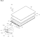
- Fig. 1 is a perspective view of a display apparatus
- Fig. 2 is a perspective view of a light source unit of the display apparatus of Fig. 1
- Fig. 3 is a side view of Fig. 2 .
- a display apparatus 100 includes a light unit 105 and a display panel 107.
- the light unit 105 includes a light source unit 101 and an optical sheet 103.
- the light unit 105 can be housed in a groove of a bottom cover (not shown).
- the display panel 107 displays image information by using light irradiated from the light unit 105.
- the display panel 107 can be made by using a liquid crystal display panel.
- the display panel 107 includes an upper substrate, a lower substrate, a liquid crystal layer interposed between the two substrates.
- the display panel 107 may further include polarized sheets which are in close contact with the top surface of the upper substrate and the bottom surface of the lower substrate respectively.
- the display panel 107 can be divided into a plurality of areas and driven in correspondence to a local dimming driving method or an impulsive driving method.
- the driving method of the display panel 107 is not limited to the aforementioned ones.
- the optical sheet 103 of the light unit 105 may be placed under the display panel 107.
- the optical sheet 103 can be detached.
- the placement of the optical sheet 103 is not limited to this.
- the optical sheet 103 may include a diffusion sheet (not shown) and/or a prism sheet (not shown).
- the diffusion sheet diffuses light emitted from a light guide plate 120 to be mentioned later.
- the diffused light is collected into a light emitting area by the prism sheet.
- the prism sheet may comprises a horizontal or/and vertical prism sheet and at least one brightness enhancement film.
- the type and number of the optical sheet 103 may be changed and are not limited to this.
- a light source unit 101 generating surface light is disposed under the optical sheet 103.
- the light source unit 101 includes a module substrate 110, a light guide plate 120, a light guide extension 130 and at least one light emitting diode 115.
- the light guide plate 120 comprises a transparent material.
- the transparent material includes at least one of an acryl resin based material like a polymethyl metaacrylate (PMMA), a polyethylene terephthlate (PET) resin, a poly carbonate (PC) resin and a polyethylene naphthalate (PEN) resin.
- PMMA polymethyl metaacrylate
- PET polyethylene terephthlate
- PC poly carbonate
- PEN polyethylene naphthalate
- the top surface thereof functioning as a surface light source is flat.
- At least one groove 122 is formed on the bottom surface of the light guide plate 120 in one direction of the bottom surface.
- a diffusion pattern may be further formed on the top surface of the light guide plate 120.
- the groove 122 may be formed to cross from one end to the other end of the light guide plate 120.
- the groove 122 includes a first surface 122a, a second surface 122b and an intersection 122c through which the first surface 122a and the second surface 122b meet each other.
- the first surface 122a may slope toward the flat of the light guide plate 120.
- the second surface 122b may be perpendicular to the flat of the light guide plate 120. However, without being limited to this, the second surface 122b may may slope toward the flat of the light guide plate 120.
- the length of the intersection 122c is equal to the longitudinal length of the groove 122. That is, the intersection 122c has a length from one end to the other end of the light guide plate 120.
- the light guide plate 120 having at least one groove 122 on one side thereof can be integrally formed with respect to one display panel 107 by employing an injection molding method or an extruding method.
- the groove 122 can be continuously formed on the bottom surface of the light guide plate 120.
- the first surface 122a and the second surface 122b may be alternately formed on the bottom surface of the light guide plate 120.
- the light guide extension 130 is formed on the second surface 122b of the groove 122 and on one lateral surface of the light guide plate 120 parallel with a longitudinal direction of the groove 122.
- the light guide extension 130 may have a rectangular parallelepiped shape.
- An adhesive member 131 is interposed between the light guide extension 130 and the light guide plate 120.
- the adhesive member 131 is, for example, made of a plastic based transparent UV bonding material.
- the light guide extension 130 may include the same material as that of the light guide plate 120.
- the light guide plate 120 may have the same refractive index as that of the adhesive member 131. Therefore, when light incident on the light guide extension 130 passes through the adhesive member 131 and is incident on the light guide plate 120, there occurs little reflection loss due to no refractive index difference, so optical characteristic is not affected.
- the light guide plate 120 and the light guide extension 130 are made of PMMA material, they and a plastic based adhesive member 131 have the same refractive index of about 1.5.
- the at least one light emitting diode 115 are arranged adjacently to one side of the light guide extension 130.
- a module substrate 110 on which the light emitting diodes 115 are mounted is arranged under each of the grooves 122.
- the module substrate 110 may comprise a metal core PCB, a FR-4 PCB, a common PCB, a flexible substrate and the like and the material of the module substrate 110 can also be variously changed.
- a plurality of the bar-typed module substrate 110 may be arranged or a single module substrate 110 having a size corresponding to the total area of a plurality of the light guide plate 120 is arranged.
- the arrangement of the module substrate 110 is not limited to this.
- the at least one light emitting diode 115 may be a white LED or a colored LED emitting at least one color among colors such as red, blue, green and the like.
- the colored LED may include a red LED, a blue LED and a green LED.
- the arrangement of the light emitting diodes and the light emitted from the light emitting diodes are changeable.
- the module substrate 110 supplies electric power to the light emitting diode 115 of each area of the light guide plate 120, thereby individually driving the light emitting diode of each area. Accordingly, the areas of the light guide plate 120 are able to emit lights having different luminances from those of others.
- the at least one light emitting diode 115 has a side light emitting type and is arranged at one side of the light guide extension 130.
- the light emitting diode 115 allows light to be incident on a lateral surface of the light guide extension 130.
- the light guide plate 120 guides light incident from the second surface 122b of the groove 122 and emits the light through the top surface in the form of a surface light.
- a reflective member 140 such as a reflective sheet, a reflective agent and a reflective plate is arranged under or on the bottom surface of the light guide plate 120 and re-reflects the light leaked from the light guide plate 120.
- the reflective member 140 may be formed under or on the bottom surface of the light guide extension 130.
- the reflective member 140 may be formed on the first surface 122a of the groove 122 of the light guide plate 120.
- the reflective member 140 is not formed on the second surface 122, that is, a light incident surface of the groove 122 of the light guide plate 120.
- the light emitted from the at least one light emitting diode 115 may be covered with the reflective member 140 formed on the first surface 122a of the groove 122 in the light emission direction.
- the light guide extension 130 is designed to have an appropriate length for hot spot not to be created.
- a plurality of the grooves 122 are formed on the bottom surface of the light guide plate 120 and at least one light emitting diode 115 is arranged at one side of each of the grooves 122. As a result, it is possible to provide an improved optical uniformity.
- the light guide plate 120 having the grooves 122 on the bottom surface thereof is integrally formed and the light guide extension 130 is adhered to each of the grooves 122 by using the adhesive member 131. Accordingly, it is possible to improve the hot spot and to obtain the optical uniformity.
- a partial driving method such as a local dimming driving method and an impulsive driving method and the like, thereby reducing power consumption, improving screen contrast and improving the image quality of the display apparatus.
- the integrally formed light guide plate 120 i.e., a backlight unit which is partially driven makes it possible to individually drive its lighting areas. It is also possible to precisely control a light quantity distribution through the individual lighting area. Moreover, the light emitting diodes are driven individually according to the sub-areas of the entire lighting area, so that the sub-areas can emit lights having different luminances from those of others. Therefore, the display apparatus can show image of enhanced quality.
- Fig. 4 is a plan view showing an individual driving method of a light unit of the display apparatus.
- the light unit 105 is driven by an entire driving method or a partial driving method.
- the partial driving method includes a local dimming driving method or an impulsive driving method and the like.
- the display panel 107 When the at least one light emitting diode 115 is driven by the local dimming driving method, the display panel 107 includes a plurality of unit lighting areas. The luminance of the at least the one light emitting diode 115 can be individually controlled according to the gray peak value of each of the unit lighting areas "A".
- each of the lighting areas is synchronized in terms of time with the display panel 107 and is sequentially lighted.
- the light guide plate 120 is integrally formed, the individual lighting area is created by the groove 122 formed on the bottom surface of the light guide plate 120. Therefore, the light unit 105 can be partially driven and an optical uniformity can be obtained. In other words, while the embodiment shows that the individual unit lighting area "A" is created on the display panel 107, this does not mean that the unit lighting area "A" is physically divided.
- the integrally formed light guide plate 120 is able to produce a high lighting quality of the boundary of each unit lighting area "A".
- the driving method of the at least one light emitting diode 115 is variously changed according to the circuit design thereof. There is no limit to the driving method of the light emitting diode 115.
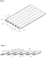
- Fig. 5 is a plan view showing an embodiment of the light unit according to the invention.
- the light guide extension and the light emitting diode arranged on the outer surface of the light guide plate are shown and described. While the light guide extension and the light emitting diode arranged inside the groove are not shown, it can be expected that the light guide extension and the light emitting diode are formed in the same shapes as those of Fig. 5 .
- a light guide extension 130 of the light unit 105 is formed to have the same length as that of each of the grooves 122.
- the light guide extension 230 is divided into two or more light guide extensions 231 and 232 with respect to the length of the edge of the light unit 105 in consideration of the specification and the light generation range of the light emitting diode 115 and.
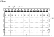
- Fig. 6 is a plan view showing further another embodiment of the light unit according to the invention.
- the light guide extension 333 of the light unit is formed corresponding one-to-one to the light emitting diodes 115 in consideration of the specification and the light generation range of the light emitting diode 115.
- a plurality of the light guide extensions 333 are adhered to one side of the light guide plate 120 and to one side of the groove by means of the adhesive member 131.
- the light emitting diodes 115 are arranged one-to-one correspondingly to the one side of the light guide extensions 333.
Landscapes
- Physics & Mathematics (AREA)
- General Physics & Mathematics (AREA)
- Optics & Photonics (AREA)
- Nonlinear Science (AREA)
- Mathematical Physics (AREA)
- Chemical & Material Sciences (AREA)
- Crystallography & Structural Chemistry (AREA)
- Planar Illumination Modules (AREA)
- Illuminated Signs And Luminous Advertising (AREA)
- Liquid Crystal (AREA)
Applications Claiming Priority (2)
| Application Number | Priority Date | Filing Date | Title |
|---|---|---|---|
| KR1020090069135A KR20110011463A (ko) | 2009-07-28 | 2009-07-28 | 라이트 유닛 및 이를 구비한 표시장치 |
| EP10169316.6A EP2280217B1 (en) | 2009-07-28 | 2010-07-12 | Light unit with light guide plate and display apparatus having the same |
Related Parent Applications (2)
| Application Number | Title | Priority Date | Filing Date |
|---|---|---|---|
| EP10169316.6A Division EP2280217B1 (en) | 2009-07-28 | 2010-07-12 | Light unit with light guide plate and display apparatus having the same |
| EP10169316.6A Division-Into EP2280217B1 (en) | 2009-07-28 | 2010-07-12 | Light unit with light guide plate and display apparatus having the same |
Publications (2)
| Publication Number | Publication Date |
|---|---|
| EP2806208A1 EP2806208A1 (en) | 2014-11-26 |
| EP2806208B1 true EP2806208B1 (en) | 2019-09-04 |
Family
ID=42650477
Family Applications (2)
| Application Number | Title | Priority Date | Filing Date |
|---|---|---|---|
| EP10169316.6A Not-in-force EP2280217B1 (en) | 2009-07-28 | 2010-07-12 | Light unit with light guide plate and display apparatus having the same |
| EP14171998.9A Active EP2806208B1 (en) | 2009-07-28 | 2010-07-12 | Light unit with light guide plate |
Family Applications Before (1)
| Application Number | Title | Priority Date | Filing Date |
|---|---|---|---|
| EP10169316.6A Not-in-force EP2280217B1 (en) | 2009-07-28 | 2010-07-12 | Light unit with light guide plate and display apparatus having the same |
Country Status (5)
| Country | Link |
|---|---|
| US (1) | US8662729B2 (da) |
| EP (2) | EP2280217B1 (da) |
| JP (1) | JP5623165B2 (da) |
| KR (1) | KR20110011463A (da) |
| CN (1) | CN101986003B (da) |
Families Citing this family (8)
| Publication number | Priority date | Publication date | Assignee | Title |
|---|---|---|---|---|
| US7872705B2 (en) * | 2007-07-29 | 2011-01-18 | Cree, Inc. | LED backlight system for LCD displays |
| KR101287493B1 (ko) * | 2010-12-23 | 2013-07-18 | 엘지이노텍 주식회사 | 백라이트유닛 및 이를 이용한 액정표시장치 |
| KR101824036B1 (ko) | 2011-06-30 | 2018-03-14 | 엘지이노텍 주식회사 | 디스플레이 장치 |
| CN102620211B (zh) * | 2012-04-05 | 2013-09-18 | 深圳市华星光电技术有限公司 | 背光模组及液晶显示器 |
| SE540740C2 (sv) * | 2015-03-24 | 2018-10-30 | Crusader Int Ab | Glasenhet |
| KR101685989B1 (ko) * | 2016-01-04 | 2016-12-13 | 엘지전자 주식회사 | 이동 단말기 |
| US10392301B2 (en) | 2016-04-15 | 2019-08-27 | Furcifer Inc. | Integration of electrochromic films on a substrate |
| US10605980B2 (en) | 2017-06-04 | 2020-03-31 | Svv Technology Innovations, Inc. | Stepped light guide illumination systems |
Family Cites Families (30)
| Publication number | Priority date | Publication date | Assignee | Title |
|---|---|---|---|---|
| JP2001312916A (ja) * | 2000-02-24 | 2001-11-09 | Sony Corp | 面光源装置 |
| JP2002042537A (ja) | 2000-07-27 | 2002-02-08 | Asahi National Lighting Co Ltd | 導光板装置 |
| US6929288B2 (en) * | 2001-12-20 | 2005-08-16 | Usui Kokusai Sangyo Kaisha Limited | Connecting structure of branch connector in fuel pressure accumulating container |
| JP4029743B2 (ja) * | 2003-02-24 | 2008-01-09 | ソニー株式会社 | バックライト |
| KR100590535B1 (ko) | 2004-01-24 | 2006-06-15 | 삼성전자주식회사 | 백라이트 유니트 |
| JP5616570B2 (ja) | 2005-04-21 | 2014-10-29 | 日亜化学工業株式会社 | 電光表示針と導光体 |
| KR101157254B1 (ko) | 2005-06-28 | 2012-06-15 | 엘지디스플레이 주식회사 | 백라이트 및 이를 구비한 액정표시장치 |
| KR100638874B1 (ko) * | 2005-07-06 | 2006-10-27 | 삼성전기주식회사 | Led 광원이 도광판에 삽입된 백라이트 장치의광원-도광판 구조 및 이를 포함하는 백라이트 장치 |
| JP2007041605A (ja) * | 2005-08-04 | 2007-02-15 | Boe Hydis Technology Co Ltd | 液晶表示装置のバックライト構造体 |
| JP4600218B2 (ja) | 2005-08-29 | 2010-12-15 | カシオ計算機株式会社 | 面光源及び液晶表示装置 |
| KR100699266B1 (ko) * | 2005-09-09 | 2007-03-27 | 삼성전자주식회사 | 백라이트 유닛과 이를 포함하는 표시장치 |
| KR101049859B1 (ko) * | 2007-11-28 | 2011-07-19 | 대한민국 | N-말단 pI 값 조절에 의한 수용성 재조합 단백질 생산방법 |
| KR100754400B1 (ko) | 2006-04-21 | 2007-08-31 | 삼성전자주식회사 | 백라이트 유닛 및 이를 채용한 디스플레이 장치 |
| WO2008032275A1 (en) | 2006-09-15 | 2008-03-20 | Koninklijke Philips Electronics N.V. | Flat and thin led-based luminary |
| CN101517754A (zh) | 2006-09-15 | 2009-08-26 | 皇家飞利浦电子股份有限公司 | 提供准直光的基于led的平薄照明设备 |
| JP2008191429A (ja) | 2007-02-06 | 2008-08-21 | Alps Electric Co Ltd | 操作ユニット |
| TW200900766A (en) * | 2007-02-21 | 2009-01-01 | Koninkl Philips Electronics Nv | Lighting system with improved rigidity |
| US20080205078A1 (en) | 2007-02-23 | 2008-08-28 | Luminus Devices, Inc. | Illumination tiles and related methods |
| JP4505554B2 (ja) | 2007-04-27 | 2010-07-21 | 株式会社日立製作所 | 表示装置 |
| JP2008293826A (ja) | 2007-05-25 | 2008-12-04 | Mitsubishi Electric Corp | 面状光源装置および表示装置 |
| KR100920229B1 (ko) | 2007-06-28 | 2009-10-05 | 포항공과대학교 산학협력단 | Bp의 고속 시스톨릭 어레이 시스템과 이를 이용한 메시지처리 방법 |
| US8040459B2 (en) * | 2007-07-27 | 2011-10-18 | Sharp Kabushiki Kaisha | Illuminating device and liquid crystal display device |
| KR20090019208A (ko) | 2007-08-20 | 2009-02-25 | 엘지디스플레이 주식회사 | 평판표시장치용 백라이트 유닛 |
| KR101565934B1 (ko) | 2008-05-23 | 2015-11-06 | 삼성디스플레이 주식회사 | 백라이트 어셈블리 및 이를 갖는 표시장치 |
| RU2456502C2 (ru) * | 2008-05-30 | 2012-07-20 | Шарп Кабусики Кайся | Устройство освещения, устройство отображения и светопроводящая пластина |
| US20110109836A1 (en) * | 2008-07-07 | 2011-05-12 | Sharp Kabushiki Kaisha | Illumination device and liquid crystal display device |
| US8405796B2 (en) * | 2008-07-14 | 2013-03-26 | Sharp Kabushiki Kaisha | Illumination device, surface light source device, and liquid crystal display device |
| KR101539956B1 (ko) * | 2008-12-16 | 2015-07-29 | 삼성디스플레이 주식회사 | 표시장치 |
| KR20100103736A (ko) * | 2009-03-10 | 2010-09-28 | 엘지이노텍 주식회사 | 라이트 유닛 및 이를 구비한 표시장치 |
| KR101611616B1 (ko) * | 2009-08-28 | 2016-04-11 | 엘지전자 주식회사 | 백라이트 유닛 및 그를 이용한 디스플레이 장치 |
-
2009
- 2009-07-28 KR KR1020090069135A patent/KR20110011463A/ko active Search and Examination
-
2010
- 2010-06-18 US US12/818,671 patent/US8662729B2/en active Active
- 2010-07-12 EP EP10169316.6A patent/EP2280217B1/en not_active Not-in-force
- 2010-07-12 EP EP14171998.9A patent/EP2806208B1/en active Active
- 2010-07-15 JP JP2010160387A patent/JP5623165B2/ja not_active Expired - Fee Related
- 2010-07-21 CN CN201010235505.8A patent/CN101986003B/zh not_active Expired - Fee Related
Non-Patent Citations (1)
| Title |
|---|
| None * |
Also Published As
| Publication number | Publication date |
|---|---|
| US8662729B2 (en) | 2014-03-04 |
| US20110026269A1 (en) | 2011-02-03 |
| JP5623165B2 (ja) | 2014-11-12 |
| CN101986003A (zh) | 2011-03-16 |
| KR20110011463A (ko) | 2011-02-08 |
| JP2011029182A (ja) | 2011-02-10 |
| EP2280217B1 (en) | 2014-08-06 |
| EP2806208A1 (en) | 2014-11-26 |
| EP2280217A1 (en) | 2011-02-02 |
| CN101986003B (zh) | 2014-09-03 |
Similar Documents
| Publication | Publication Date | Title |
|---|---|---|
| EP2806208B1 (en) | Light unit with light guide plate | |
| TWI529459B (zh) | 背光單元及具有其之顯示裝置 | |
| JP5085645B2 (ja) | 発光素子および液晶表示装置 | |
| US7201488B2 (en) | Planar light source apparatus and liquid display apparatus | |
| JP4529573B2 (ja) | 面状光源装置及び液晶表示装置 | |
| US8292447B2 (en) | Backlight unit and display apparatus having the same | |
| CN101832491B (zh) | 光源和具有该光源的显示设备 | |
| JP2009128647A (ja) | 液晶表示装置 | |
| US20080291694A1 (en) | Planar light source device and display device | |
| KR20100095812A (ko) | 백 라이트 유닛 및 이를 포함하는 액정표시장치 | |
| KR101637592B1 (ko) | 백라이트 유닛 및 이를 포함하는 표시 장치 | |
| KR101734545B1 (ko) | 라이트 유닛 및 표시장치 | |
| KR20090081664A (ko) | 발광 다이오드 백라이트 유닛 및 이를 구비한 액정표시장치 | |
| JP2008047482A (ja) | 照明装置、液晶装置及び電子機器 | |
| KR20070077255A (ko) | 발광다이오드를 갖는 백라이트 어셈블리 | |
| KR20110139365A (ko) | 백라이트 유닛 및 이를 포함하는 표시 장치 | |
| KR20120016973A (ko) | 백라이트 유닛 | |
| KR20110139364A (ko) | 백라이트 유닛 및 이를 포함하는 표시 장치 | |
| KR20110136651A (ko) | 백라이트 유닛 및 이를 포함하는 표시 장치 | |
| KR20120016971A (ko) | 백라이트 유닛 | |
| KR20110136650A (ko) | 백라이트 유닛 및 이를 포함하는 표시 장치 | |
| KR20120016970A (ko) | 백라이트 유닛 | |
| KR20110136648A (ko) | 백라이트 유닛 및 이를 포함하는 표시 장치 |
Legal Events
| Date | Code | Title | Description |
|---|---|---|---|
| PUAI | Public reference made under article 153(3) epc to a published international application that has entered the european phase |
Free format text: ORIGINAL CODE: 0009012 |
|
| 17P | Request for examination filed |
Effective date: 20140611 |
|
| AC | Divisional application: reference to earlier application |
Ref document number: 2280217 Country of ref document: EP Kind code of ref document: P |
|
| AK | Designated contracting states |
Kind code of ref document: A1 Designated state(s): AL AT BE BG CH CY CZ DE DK EE ES FI FR GB GR HR HU IE IS IT LI LT LU LV MC MK MT NL NO PL PT RO SE SI SK SM TR |
|
| R17P | Request for examination filed (corrected) |
Effective date: 20150526 |
|
| RBV | Designated contracting states (corrected) |
Designated state(s): AL AT BE BG CH CY CZ DE DK EE ES FI FR GB GR HR HU IE IS IT LI LT LU LV MC MK MT NL NO PL PT RO SE SI SK SM TR |
|
| RAP1 | Party data changed (applicant data changed or rights of an application transferred) |
Owner name: LG INNOTEK CO., LTD. |
|
| STAA | Information on the status of an ep patent application or granted ep patent |
Free format text: STATUS: EXAMINATION IS IN PROGRESS |
|
| 17Q | First examination report despatched |
Effective date: 20171214 |
|
| GRAP | Despatch of communication of intention to grant a patent |
Free format text: ORIGINAL CODE: EPIDOSNIGR1 |
|
| STAA | Information on the status of an ep patent application or granted ep patent |
Free format text: STATUS: GRANT OF PATENT IS INTENDED |
|
| INTG | Intention to grant announced |
Effective date: 20190227 |
|
| RIN1 | Information on inventor provided before grant (corrected) |
Inventor name: OH, NAM SEOK |
|
| GRAS | Grant fee paid |
Free format text: ORIGINAL CODE: EPIDOSNIGR3 |
|
| GRAA | (expected) grant |
Free format text: ORIGINAL CODE: 0009210 |
|
| STAA | Information on the status of an ep patent application or granted ep patent |
Free format text: STATUS: THE PATENT HAS BEEN GRANTED |
|
| AC | Divisional application: reference to earlier application |
Ref document number: 2280217 Country of ref document: EP Kind code of ref document: P |
|
| AK | Designated contracting states |
Kind code of ref document: B1 Designated state(s): AL AT BE BG CH CY CZ DE DK EE ES FI FR GB GR HR HU IE IS IT LI LT LU LV MC MK MT NL NO PL PT RO SE SI SK SM TR |
|
| REG | Reference to a national code |
Ref country code: GB Ref legal event code: FG4D |
|
| REG | Reference to a national code |
Ref country code: CH Ref legal event code: EP |
|
| REG | Reference to a national code |
Ref country code: AT Ref legal event code: REF Ref document number: 1175857 Country of ref document: AT Kind code of ref document: T Effective date: 20190915 |
|
| REG | Reference to a national code |
Ref country code: DE Ref legal event code: R096 Ref document number: 602010060951 Country of ref document: DE |
|
| REG | Reference to a national code |
Ref country code: IE Ref legal event code: FG4D |
|
| REG | Reference to a national code |
Ref country code: NL Ref legal event code: MP Effective date: 20190904 |
|
| REG | Reference to a national code |
Ref country code: LT Ref legal event code: MG4D |
|
| PG25 | Lapsed in a contracting state [announced via postgrant information from national office to epo] |
Ref country code: SE Free format text: LAPSE BECAUSE OF FAILURE TO SUBMIT A TRANSLATION OF THE DESCRIPTION OR TO PAY THE FEE WITHIN THE PRESCRIBED TIME-LIMIT Effective date: 20190904 Ref country code: HR Free format text: LAPSE BECAUSE OF FAILURE TO SUBMIT A TRANSLATION OF THE DESCRIPTION OR TO PAY THE FEE WITHIN THE PRESCRIBED TIME-LIMIT Effective date: 20190904 Ref country code: LT Free format text: LAPSE BECAUSE OF FAILURE TO SUBMIT A TRANSLATION OF THE DESCRIPTION OR TO PAY THE FEE WITHIN THE PRESCRIBED TIME-LIMIT Effective date: 20190904 Ref country code: FI Free format text: LAPSE BECAUSE OF FAILURE TO SUBMIT A TRANSLATION OF THE DESCRIPTION OR TO PAY THE FEE WITHIN THE PRESCRIBED TIME-LIMIT Effective date: 20190904 Ref country code: NO Free format text: LAPSE BECAUSE OF FAILURE TO SUBMIT A TRANSLATION OF THE DESCRIPTION OR TO PAY THE FEE WITHIN THE PRESCRIBED TIME-LIMIT Effective date: 20191204 Ref country code: BG Free format text: LAPSE BECAUSE OF FAILURE TO SUBMIT A TRANSLATION OF THE DESCRIPTION OR TO PAY THE FEE WITHIN THE PRESCRIBED TIME-LIMIT Effective date: 20191204 |
|
| PG25 | Lapsed in a contracting state [announced via postgrant information from national office to epo] |
Ref country code: ES Free format text: LAPSE BECAUSE OF FAILURE TO SUBMIT A TRANSLATION OF THE DESCRIPTION OR TO PAY THE FEE WITHIN THE PRESCRIBED TIME-LIMIT Effective date: 20190904 Ref country code: LV Free format text: LAPSE BECAUSE OF FAILURE TO SUBMIT A TRANSLATION OF THE DESCRIPTION OR TO PAY THE FEE WITHIN THE PRESCRIBED TIME-LIMIT Effective date: 20190904 Ref country code: GR Free format text: LAPSE BECAUSE OF FAILURE TO SUBMIT A TRANSLATION OF THE DESCRIPTION OR TO PAY THE FEE WITHIN THE PRESCRIBED TIME-LIMIT Effective date: 20191205 Ref country code: AL Free format text: LAPSE BECAUSE OF FAILURE TO SUBMIT A TRANSLATION OF THE DESCRIPTION OR TO PAY THE FEE WITHIN THE PRESCRIBED TIME-LIMIT Effective date: 20190904 |
|
| REG | Reference to a national code |
Ref country code: AT Ref legal event code: MK05 Ref document number: 1175857 Country of ref document: AT Kind code of ref document: T Effective date: 20190904 |
|
| PG25 | Lapsed in a contracting state [announced via postgrant information from national office to epo] |
Ref country code: PT Free format text: LAPSE BECAUSE OF FAILURE TO SUBMIT A TRANSLATION OF THE DESCRIPTION OR TO PAY THE FEE WITHIN THE PRESCRIBED TIME-LIMIT Effective date: 20200106 Ref country code: IT Free format text: LAPSE BECAUSE OF FAILURE TO SUBMIT A TRANSLATION OF THE DESCRIPTION OR TO PAY THE FEE WITHIN THE PRESCRIBED TIME-LIMIT Effective date: 20190904 Ref country code: RO Free format text: LAPSE BECAUSE OF FAILURE TO SUBMIT A TRANSLATION OF THE DESCRIPTION OR TO PAY THE FEE WITHIN THE PRESCRIBED TIME-LIMIT Effective date: 20190904 Ref country code: AT Free format text: LAPSE BECAUSE OF FAILURE TO SUBMIT A TRANSLATION OF THE DESCRIPTION OR TO PAY THE FEE WITHIN THE PRESCRIBED TIME-LIMIT Effective date: 20190904 Ref country code: NL Free format text: LAPSE BECAUSE OF FAILURE TO SUBMIT A TRANSLATION OF THE DESCRIPTION OR TO PAY THE FEE WITHIN THE PRESCRIBED TIME-LIMIT Effective date: 20190904 Ref country code: PL Free format text: LAPSE BECAUSE OF FAILURE TO SUBMIT A TRANSLATION OF THE DESCRIPTION OR TO PAY THE FEE WITHIN THE PRESCRIBED TIME-LIMIT Effective date: 20190904 Ref country code: EE Free format text: LAPSE BECAUSE OF FAILURE TO SUBMIT A TRANSLATION OF THE DESCRIPTION OR TO PAY THE FEE WITHIN THE PRESCRIBED TIME-LIMIT Effective date: 20190904 |
|
| PG25 | Lapsed in a contracting state [announced via postgrant information from national office to epo] |
Ref country code: SK Free format text: LAPSE BECAUSE OF FAILURE TO SUBMIT A TRANSLATION OF THE DESCRIPTION OR TO PAY THE FEE WITHIN THE PRESCRIBED TIME-LIMIT Effective date: 20190904 Ref country code: IS Free format text: LAPSE BECAUSE OF FAILURE TO SUBMIT A TRANSLATION OF THE DESCRIPTION OR TO PAY THE FEE WITHIN THE PRESCRIBED TIME-LIMIT Effective date: 20200224 Ref country code: SM Free format text: LAPSE BECAUSE OF FAILURE TO SUBMIT A TRANSLATION OF THE DESCRIPTION OR TO PAY THE FEE WITHIN THE PRESCRIBED TIME-LIMIT Effective date: 20190904 Ref country code: CZ Free format text: LAPSE BECAUSE OF FAILURE TO SUBMIT A TRANSLATION OF THE DESCRIPTION OR TO PAY THE FEE WITHIN THE PRESCRIBED TIME-LIMIT Effective date: 20190904 |
|
| REG | Reference to a national code |
Ref country code: DE Ref legal event code: R097 Ref document number: 602010060951 Country of ref document: DE |
|
| PLBE | No opposition filed within time limit |
Free format text: ORIGINAL CODE: 0009261 |
|
| STAA | Information on the status of an ep patent application or granted ep patent |
Free format text: STATUS: NO OPPOSITION FILED WITHIN TIME LIMIT |
|
| PG2D | Information on lapse in contracting state deleted |
Ref country code: IS |
|
| PG25 | Lapsed in a contracting state [announced via postgrant information from national office to epo] |
Ref country code: DK Free format text: LAPSE BECAUSE OF FAILURE TO SUBMIT A TRANSLATION OF THE DESCRIPTION OR TO PAY THE FEE WITHIN THE PRESCRIBED TIME-LIMIT Effective date: 20190904 Ref country code: IS Free format text: LAPSE BECAUSE OF FAILURE TO SUBMIT A TRANSLATION OF THE DESCRIPTION OR TO PAY THE FEE WITHIN THE PRESCRIBED TIME-LIMIT Effective date: 20200105 |
|
| 26N | No opposition filed |
Effective date: 20200605 |
|
| PG25 | Lapsed in a contracting state [announced via postgrant information from national office to epo] |
Ref country code: SI Free format text: LAPSE BECAUSE OF FAILURE TO SUBMIT A TRANSLATION OF THE DESCRIPTION OR TO PAY THE FEE WITHIN THE PRESCRIBED TIME-LIMIT Effective date: 20190904 |
|
| PG25 | Lapsed in a contracting state [announced via postgrant information from national office to epo] |
Ref country code: MC Free format text: LAPSE BECAUSE OF FAILURE TO SUBMIT A TRANSLATION OF THE DESCRIPTION OR TO PAY THE FEE WITHIN THE PRESCRIBED TIME-LIMIT Effective date: 20190904 |
|
| REG | Reference to a national code |
Ref country code: CH Ref legal event code: PL |
|
| GBPC | Gb: european patent ceased through non-payment of renewal fee |
Effective date: 20200712 |
|
| REG | Reference to a national code |
Ref country code: BE Ref legal event code: MM Effective date: 20200731 |
|
| PG25 | Lapsed in a contracting state [announced via postgrant information from national office to epo] |
Ref country code: CH Free format text: LAPSE BECAUSE OF NON-PAYMENT OF DUE FEES Effective date: 20200731 Ref country code: GB Free format text: LAPSE BECAUSE OF NON-PAYMENT OF DUE FEES Effective date: 20200712 Ref country code: LI Free format text: LAPSE BECAUSE OF NON-PAYMENT OF DUE FEES Effective date: 20200731 Ref country code: LU Free format text: LAPSE BECAUSE OF NON-PAYMENT OF DUE FEES Effective date: 20200712 Ref country code: FR Free format text: LAPSE BECAUSE OF NON-PAYMENT OF DUE FEES Effective date: 20200731 |
|
| PG25 | Lapsed in a contracting state [announced via postgrant information from national office to epo] |
Ref country code: BE Free format text: LAPSE BECAUSE OF NON-PAYMENT OF DUE FEES Effective date: 20200731 |
|
| PG25 | Lapsed in a contracting state [announced via postgrant information from national office to epo] |
Ref country code: IE Free format text: LAPSE BECAUSE OF NON-PAYMENT OF DUE FEES Effective date: 20200712 |
|
| REG | Reference to a national code |
Ref country code: DE Ref legal event code: R081 Ref document number: 602010060951 Country of ref document: DE Owner name: SUZHOU LEKIN SEMICONDUCTOR CO. LTD., TAICANG, CN Free format text: FORMER OWNER: LG INNOTEK CO., LTD., SEOUL, KR |
|
| PG25 | Lapsed in a contracting state [announced via postgrant information from national office to epo] |
Ref country code: TR Free format text: LAPSE BECAUSE OF FAILURE TO SUBMIT A TRANSLATION OF THE DESCRIPTION OR TO PAY THE FEE WITHIN THE PRESCRIBED TIME-LIMIT Effective date: 20190904 Ref country code: MT Free format text: LAPSE BECAUSE OF FAILURE TO SUBMIT A TRANSLATION OF THE DESCRIPTION OR TO PAY THE FEE WITHIN THE PRESCRIBED TIME-LIMIT Effective date: 20190904 Ref country code: CY Free format text: LAPSE BECAUSE OF FAILURE TO SUBMIT A TRANSLATION OF THE DESCRIPTION OR TO PAY THE FEE WITHIN THE PRESCRIBED TIME-LIMIT Effective date: 20190904 |
|
| PG25 | Lapsed in a contracting state [announced via postgrant information from national office to epo] |
Ref country code: MK Free format text: LAPSE BECAUSE OF FAILURE TO SUBMIT A TRANSLATION OF THE DESCRIPTION OR TO PAY THE FEE WITHIN THE PRESCRIBED TIME-LIMIT Effective date: 20190904 |
|
| PGFP | Annual fee paid to national office [announced via postgrant information from national office to epo] |
Ref country code: DE Payment date: 20230607 Year of fee payment: 14 |