EP2804180A1 - Mehrstufiger MRAM für geringen Stromverbrauch und zuverlässiger Schreiboperation - Google Patents
Mehrstufiger MRAM für geringen Stromverbrauch und zuverlässiger Schreiboperation Download PDFInfo
- Publication number
- EP2804180A1 EP2804180A1 EP13290108.3A EP13290108A EP2804180A1 EP 2804180 A1 EP2804180 A1 EP 2804180A1 EP 13290108 A EP13290108 A EP 13290108A EP 2804180 A1 EP2804180 A1 EP 2804180A1
- Authority
- EP
- European Patent Office
- Prior art keywords
- storage
- tunnel junction
- magnetization
- storage layer
- magnetic tunnel
- Prior art date
- Legal status (The legal status is an assumption and is not a legal conclusion. Google has not performed a legal analysis and makes no representation as to the accuracy of the status listed.)
- Withdrawn
Links
Images


Classifications
-
- G—PHYSICS
- G11—INFORMATION STORAGE
- G11C—STATIC STORES
- G11C11/00—Digital stores characterised by the use of particular electric or magnetic storage elements; Storage elements therefor
- G11C11/02—Digital stores characterised by the use of particular electric or magnetic storage elements; Storage elements therefor using magnetic elements
- G11C11/16—Digital stores characterised by the use of particular electric or magnetic storage elements; Storage elements therefor using magnetic elements using elements in which the storage effect is based on magnetic spin effect
- G11C11/165—Auxiliary circuits
- G11C11/1675—Writing or programming circuits or methods
-
- G—PHYSICS
- G11—INFORMATION STORAGE
- G11C—STATIC STORES
- G11C11/00—Digital stores characterised by the use of particular electric or magnetic storage elements; Storage elements therefor
- G11C11/02—Digital stores characterised by the use of particular electric or magnetic storage elements; Storage elements therefor using magnetic elements
- G11C11/16—Digital stores characterised by the use of particular electric or magnetic storage elements; Storage elements therefor using magnetic elements using elements in which the storage effect is based on magnetic spin effect
- G11C11/161—Digital stores characterised by the use of particular electric or magnetic storage elements; Storage elements therefor using magnetic elements using elements in which the storage effect is based on magnetic spin effect details concerning the memory cell structure, e.g. the layers of the ferromagnetic memory cell
-
- G—PHYSICS
- G11—INFORMATION STORAGE
- G11C—STATIC STORES
- G11C11/00—Digital stores characterised by the use of particular electric or magnetic storage elements; Storage elements therefor
- G11C11/56—Digital stores characterised by the use of particular electric or magnetic storage elements; Storage elements therefor using storage elements with more than two stable states represented by steps, e.g. of voltage, current, phase, frequency
- G11C11/5607—Digital stores characterised by the use of particular electric or magnetic storage elements; Storage elements therefor using storage elements with more than two stable states represented by steps, e.g. of voltage, current, phase, frequency using magnetic storage elements
Definitions
- the present disclosure concerns a multilevel thermally assisted MRAM cell for writing a plurality of data states with lower power consumption and improved reliability compared to conventional MRAM cells.
- MRAM cells comprise a magnetic tunnel junction comprising a ferromagnetic reference layer having a fixed magnetization and a ferromagnetic storage layer.
- the resistance of the cell is determined by the orientation of the storage layer magnetization relative to the orientation of the reference layer magnetization. For example, when the magnetizations of the two layers are oriented parallel the resistance is low (corresponding to a data state "0"). Conversely, when the magnetizations of the two layers are oriented anti- parallel the resistance is high (corresponding to a data state "1").
- the storage layer magnetization can be pinned by an antiferromagnetic layer when the magnetic tunnel junction is at a low threshold temperature, being at or below a blocking temperature of the antiferromagnetic layer.
- the magnetic tunnel junction is heated above the blocking temperature, or at a high threshold temperature, such as to free the storage layer magnetization.
- the blocking temperature is typically between 150°C to 300°C such that TAS MRAM cells have increased stability at normal operating temperatures, i.e., when the MRAM cell is not written. In other words, the pinned storage layer magnetization is not affected by external fields and noise.
- the orientation of the reference layer magnetization can be freely varied with an external applied magnetic field.
- the orientation of the reference layer magnetization is varied and compared to the storage layer magnetization being pinned.
- MRAM cells with a multilevel state write operation have also been proposed, allowing for writing more than the two level states "0" and "1" as described above.
- Such multilevel MRAM cell can be based on orienting the storage layer magnetization in various intermediate positions between the parallel and antiparallel orientations using relatively low magnetic fields.
- Such multilevel MRAM cells require at least two current lines increasing the complexity of the cell.
- it is difficult to obtain reproducible write at low field due to variations in the orientation of storage layer magnetization caused by irregularities in the storage layer. Such irregularities are typically shape and/or edge roughness generated by the fabrication process of the storage layer.
- the present disclosure concerns a MRAM cell comprising a magnetic tunnel junction comprising a storage layer having a storage magnetization, a reference layer having a reference magnetization and a barrier layer between the storage and reference layer; the magnetic tunnel junction further comprising an antiferromagnetic layer exchange-coupling the storage layer such as to pin the storage magnetization at a low temperature threshold and free it at a high temperature threshold; the storage layer being arranged such that the storage magnetization comprises a micromagnetic object that is movable within the storage layer (23) when the magnetic tunnel junction is at the high temperature threshold and a write data is applied; the resistance of the magnetic tunnel junction being determined by the relative position of the micromagnetic object in the storage layer within the storage layer.
- said micromagnetic object can comprise a magnetic vortex with a vortex center, the resistance of the magnetic tunnel junction being determined by the position of the vortex center within the storage layer.
- the storage layer can have an aspect ratio below 3.
- said micromagnetic object can comprise a domain wall defining two magnetic domains; and the resistance of the magnetic tunnel junction can be determined by the relative size of the two magnetic domains, which is determined by the domain wall position.
- the storage layer can have an aspect ratio being comprised between 1.5 and 5.
- the storage layer can be rectangular, diamond or elliptical shaped.
- the storage layer can have a thickness being smaller than 200 nm and preferably smaller than 20 nm.
- the storage layer can further comprise a FeNi -based alloy.
- the reference magnetization can be fixed or can be freely switchable with an external applied magnetic field.
- the present disclosure also pertains to a method for writing to the MRAM cell comprising:
- applying the write data comprises passing a field current in the MRAM cell such as to generate a write magnetic field adapted for moving the vortex center or domain wall.
- Applying the write data can comprise passing a spin-polarized current in the magnetic tunnel junction, the domain wall or the vortex center position being determined by the magnitude and polarity of the spin-polarized current.
- said write data can be applied such as to move the micromagnetic object to a plurality of distinct positions corresponding to a plurality of distinct magnetoresistance values, respectively.
- the plurality of distinct positions can be comprised between two and ten such that the magnetoresistance of the magnetic tunnel junction can be varied between two and ten distinct values.
- the MRAM cell disclosed herein allows for writing a plurality of data states with lower power consumption and improved reliability compared to conventional MRAM cells.
- Fig. 1 illustrates a MRAM cell 1 according to an embodiment.
- the MRAM cell 1 comprises a magnetic tunnel junction 2 comprising a storage layer 23 having a storage magnetization 230, a reference layer 21 having a reference magnetization 210 and a barrier layer 22 between the storage and reference layer 23, 21.
- the magnetic tunnel junction 2 further comprises an antiferromagnetic layer 24 exchange-coupling the storage layer 23 such as to pin the storage magnetization 230 at a low temperature threshold and free it at a high temperature threshold.
- the MRAM cell 1 further comprises a current line 3 in electrical contact with one end of the magnetic tunnel junction 2.
- the current line 3 is arranged for passing a write data 33, 41.
- the storage layer 23 is arranged such that the storage magnetization 230 comprises a single magnetic vortex 71 within the storage layer 23.
- the vortex 71 comprises a micromagnetic object, or vortex center 7 in the storage layer 23, with magnetization perpendicular to the plane of the storage layer 23 and the main part of the magnetization 230 with an in-plane flux-closure magnetization distribution.
- the direction and the magnitude of the storage magnetization 230 depend on the position of the magnetic vortex 7.
- the configuration of the magnetic vortex 71 is represented by the little arrows.
- the magnetic vortex 71 can be moved by applying the write data 33, 41 when the magnetic tunnel junction 2 is heated at the high temperature threshold.
- a resistance R of the magnetic tunnel junction 2 is thus determined by the orientation and the magnitude of the storage magnetization 230, depending in turn of the position of the vortex center 7.
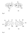
- FIG. 3a shows the storage layer 23 where the domain wall 6 is positioned such that the magnetic domain 61 on the right side is larger than the one on the left side, such that the resulting storage magnetization 230 being oriented towards the left.
- the domain wall 6 is positioned such that the magnetic domain 61 on the left side is larger than the one on the right side such that the resulting storage magnetization 230 being oriented towards the right.
- a method for writing to the MRAM cell 1 comprises:
- Heating the magnetic tunnel junction 2 can be performed by passing a heating current 32 in the magnetic tunnel junction 2 via the current line 3. Cooling (in the absence of the heating current 32) is required for stabilizing the position of the vortex center 7 or domain wall 6 and thus, stabilizing the written data state.
- applying the write data is performed by passing a spin-polarized current 33 in the magnetic tunnel junction 2 via the current line 3.
- the spin-polarized current 33 exerts a torque on the storage magnetization 230 and the domain wall 6, or the vortex center position 7, is determined by the magnitude and polarity of the spin-polarized current 33.
- a read operation of the MRAM cell 1 can comprise a step of passing a read current 31 in the magnetic tunnel junction, for example via the current line 3.
- the voltage measured across the magnetic tunnel junction 2 yields the resistance R of the magnetic tunnel junction 2, which value depends on the orientation of the fixed reference magnetization 210 relative to the resulting orientation of the storage magnetization 230.
- a self-referenced read operation of the MRAM cell 1 can comprise:
- the first and second read magnetic field 52, 53 can be applied by passing a read field current 51 in the current line 3, wherein the read field current 51 has a first polarity and a second polarity opposed to the first polarity, respectively.
- the write field current 41 and the read field current 51 with the first polarity are represented in Fig. 1 exiting the page and the corresponding write magnetic field 42 and first read magnetic field 52, respectively, by the arrow drawn with a plain line.
- the read field current 51 with the second polarity is represented entering the page and the second read magnetic field 53 is represented by the arrow in phantom line.
- the first resistance value R 1 can be compared with the second resistance value R 2 such as to determine the data written in the MRAM cell 1.
- the storage magnetization 230 having a single domain wall 6 can be obtained by the storage layer 23 having a shape with a high aspect ratio.
- the shape of the storage layer 23 can be further optimized such as to facilitates the propagation of the domain wall 6.
- a high aspect ratio of the storage layer 23 allows for increasing the length of accessible position of the domain wall 6 in the pillar, thus increasing the resistance difference between the different stored states.
- the aspect ratio should not be too high such as to avoid having more than one domain wall 6 in the storage layer 23.
- the storage layer 23 has an aspect ratio being comprised between 1.5 and 5.
- the storage layer 23 can have a rectangular shape, allowing moving the domain wall 6 or the vortex center 7 with the write magnetic field 42 having a magnitude being comprised between 5 Oe and 100 Oe, and preferably between 10 Oe and 20 Oe (corresponding to the write field current 41 having a few milliamps).
- the rectangular shape of the storage layer 23 can further have rounded edges such as to ensure a proper magnetic state with a unique domain wall 6 or vortex center 7.
- the storage layer 23 can further have a diamond shape or an elliptical shape.
- the storage layer 23 can have a small aspect ratio, preferably below 3.
- the storage layer 23 can be circular or square-shaped.
- the storage layer 23 can further have a thickness being smaller than 200 nm and preferably smaller than 20 nm.
- the storage layer 23 can further comprise a FeNi -based alloy or any alloy that allows for stabilizing the domain wall 6 or the vortex center 7.
- the write magnetic field 42 is applied such that the vortex center 7 or domain wall 6 of the storage magnetization 230 can be moved in a plurality of distinct positions, such as to write a plurality of data states in the MRAM cell 1.
- the write data 33, 41 is applied such as to move the domain wall 6 of the storage magnetization 230 in four distinct positions.
- Fig. 4a shows the domain wall 6 being moved in a first position such that the first magnetic domain 61 with the storage magnetization 230 oriented towards the right is much smaller than the second magnetic domain 61 with the storage magnetization 230 oriented towards the left, resulting in the storage magnetization 230 being substantially oriented towards the left and having a large magnitude.
- FIG. 4d shows the domain wall 6 being moved in a fourth position such that the second magnetic domain 61 with the storage magnetization 230 oriented towards the left is much smaller than the first magnetic domain 61 with the storage magnetization 230 oriented towards the right, resulting in the storage magnetization 230 being substantially oriented towards the right and having a large magnitude.
- Figs. 4b and 4c shows the second and third intermediate positions of the domain wall 6 where the magnetic domains 61 are such that a small resulting storage magnetization 230 is oriented towards the left ( Fig. 4b ) or towards the right ( Fig. 4c ) and having a smaller magnitude than in case a and d.
- Each distinct position of the domain wall 6 corresponds to a distinct resistance R of the magnetic tunnel junction 2.
- the resistance R of the magnetic tunnel junction 2 measured during the read operation, will yield a resistance value R 1 that is minimum in the configuration of Fig. 4a and increasing from the first intermediate value R 2 (configuration of Fig. 4b ) to the second intermediate value R 3 (configuration of Fig. 4c ), and maximum R 4 in the configuration of Fig. 4d .
- the distinct positions of the domain wall 6 are such that the difference in resistance R of the magnetic tunnel junction 2 between each position (or the difference between R 1 , R 2 , R 3 and R 4 ) is substantially equal.
- the equal difference between each subsequent resistance R 1 , R 2 , R 3 and R 4 can be obtained for example by the storage layer 23 having an elliptical shape, a diamond shape, or any shape that provides proper micromagnetic state.
- the domain wall 6 of the storage magnetization 230 can be moved within the storage layer 23 between two and ten distinct positions. Each distinct position of the domain wall 6 corresponds to a distinct value of the resistance R of the magnetic tunnel junction 2.
- the vortex center 7, and thus of the magnetic vortex 71 can be moved within the storage layer 23 between a plurality of distinct positions.
- a plurality of distinct resistances R can thus be obtained, each distinct resistance R being determined by the orientation and the magnitude of the storage magnetization 230 in accordance to the position of the vortex center 7.
- the vortex center 7 can be moved between two and ten distinct positions such as to obtain between two and ten distinct resistances R of the magnetic tunnel junction 2.
- the highest and lowest resistance R is obtained by saturating the storage magnetization 230 in a first direction or a second direction opposite to the first direction. Saturating the storage magnetization 230 results in moving the vortex center 7, or domain wall 6, outside the storage layer 23, i.e., the storage magnetization does not comprise the vortex center 7, or domain wall 6.
- the vortex center 7, or domain wall 6, can be reformed by applying the appropriate writing magnetic field 42 or by passing the appropriate spin-polarized current 33.
- the domain wall 6 or the vortex center position is determined by the applied writing field 42 magnitude and direction.
Priority Applications (1)
| Application Number | Priority Date | Filing Date | Title |
|---|---|---|---|
| EP13290108.3A EP2804180A1 (de) | 2013-05-15 | 2013-05-15 | Mehrstufiger MRAM für geringen Stromverbrauch und zuverlässiger Schreiboperation |
Applications Claiming Priority (1)
| Application Number | Priority Date | Filing Date | Title |
|---|---|---|---|
| EP13290108.3A EP2804180A1 (de) | 2013-05-15 | 2013-05-15 | Mehrstufiger MRAM für geringen Stromverbrauch und zuverlässiger Schreiboperation |
Publications (1)
| Publication Number | Publication Date |
|---|---|
| EP2804180A1 true EP2804180A1 (de) | 2014-11-19 |
Family
ID=48672530
Family Applications (1)
| Application Number | Title | Priority Date | Filing Date |
|---|---|---|---|
| EP13290108.3A Withdrawn EP2804180A1 (de) | 2013-05-15 | 2013-05-15 | Mehrstufiger MRAM für geringen Stromverbrauch und zuverlässiger Schreiboperation |
Country Status (1)
| Country | Link |
|---|---|
| EP (1) | EP2804180A1 (de) |
Cited By (2)
| Publication number | Priority date | Publication date | Assignee | Title |
|---|---|---|---|---|
| US9721636B1 (en) | 2016-01-28 | 2017-08-01 | Western Digital Technologies, Inc. | Method for controlled switching of a MRAM device |
| US10056126B1 (en) | 2017-10-27 | 2018-08-21 | Honeywell International Inc. | Magnetic tunnel junction based memory device |
Citations (5)
| Publication number | Priority date | Publication date | Assignee | Title |
|---|---|---|---|---|
| WO2008090305A1 (en) * | 2007-01-27 | 2008-07-31 | University Of Durham | Magnetic structure with multiple-bit storage capabilities |
| US20080205125A1 (en) * | 2007-02-27 | 2008-08-28 | Takeshi Kajiyama | Magnetic random access memory and write method thereof |
| US20090027948A1 (en) * | 2007-07-24 | 2009-01-29 | Manfred Ruehrig | Integrated Circuits, Method of Programming a Cell, Thermal Select Magnetoresistive Element, Memory Module |
| EP2109111A1 (de) * | 2008-04-07 | 2009-10-14 | Crocus Technology S.A. | System und Verfahren zum Schreiben von Daten auf magnetoresistive Direktzugriffsspeicherzellen |
| US20100097848A1 (en) * | 2008-10-16 | 2010-04-22 | Sony Corporation | Information storage element and method of writing/reading information into/from information storage element |
-
2013
- 2013-05-15 EP EP13290108.3A patent/EP2804180A1/de not_active Withdrawn
Patent Citations (5)
| Publication number | Priority date | Publication date | Assignee | Title |
|---|---|---|---|---|
| WO2008090305A1 (en) * | 2007-01-27 | 2008-07-31 | University Of Durham | Magnetic structure with multiple-bit storage capabilities |
| US20080205125A1 (en) * | 2007-02-27 | 2008-08-28 | Takeshi Kajiyama | Magnetic random access memory and write method thereof |
| US20090027948A1 (en) * | 2007-07-24 | 2009-01-29 | Manfred Ruehrig | Integrated Circuits, Method of Programming a Cell, Thermal Select Magnetoresistive Element, Memory Module |
| EP2109111A1 (de) * | 2008-04-07 | 2009-10-14 | Crocus Technology S.A. | System und Verfahren zum Schreiben von Daten auf magnetoresistive Direktzugriffsspeicherzellen |
| US20100097848A1 (en) * | 2008-10-16 | 2010-04-22 | Sony Corporation | Information storage element and method of writing/reading information into/from information storage element |
Cited By (2)
| Publication number | Priority date | Publication date | Assignee | Title |
|---|---|---|---|---|
| US9721636B1 (en) | 2016-01-28 | 2017-08-01 | Western Digital Technologies, Inc. | Method for controlled switching of a MRAM device |
| US10056126B1 (en) | 2017-10-27 | 2018-08-21 | Honeywell International Inc. | Magnetic tunnel junction based memory device |
Similar Documents
| Publication | Publication Date | Title |
|---|---|---|
| US10354710B2 (en) | Magnetoelectric random access memory array and methods of operating the same | |
| US9721637B2 (en) | Method of writing to a spin torque magnetic random access memory | |
| JP4620459B2 (ja) | 改良された記憶密度を備えた多値mram | |
| US7881099B2 (en) | Multibit magnetic random access memory device | |
| US8514615B2 (en) | Structures and methods for a field-reset spin-torque MRAM | |
| KR100604913B1 (ko) | 멀티 비트 셀 어레이 구조를 가지는 마그네틱 램 | |
| US20150213867A1 (en) | Multi-level cell designs for high density low power gshe-stt mram | |
| US7133309B2 (en) | Method and structure for generating offset fields for use in MRAM devices | |
| CN105280214A (zh) | 电流驱动型磁随机存取存储器和自旋逻辑器件 | |
| KR20060048867A (ko) | 보텍스 자기 랜덤 액세스 메모리 | |
| US9576635B2 (en) | Thermally-assisted magnetic writing device | |
| US8139397B2 (en) | Spatial correlation of reference cells in resistive memory array | |
| US9799384B2 (en) | Multi-bit MRAM cell and method for writing and reading to such MRAM cell | |
| JPWO2007111319A1 (ja) | 磁気ランダムアクセスメモリ及びその動作方法 | |
| KR20060124578A (ko) | 자기저항효과에 의해 데이터를 기억하는 자기기억소자 | |
| US6798690B1 (en) | Magnetic switching with expanded hard-axis magnetization volume at magnetoresistive bit ends | |
| JPWO2007111318A1 (ja) | 磁気ランダムアクセスメモリ及びその動作方法 | |
| US7548452B2 (en) | MRAM read bit with askew fixed layer | |
| EP2804180A1 (de) | Mehrstufiger MRAM für geringen Stromverbrauch und zuverlässiger Schreiboperation | |
| RU2704732C1 (ru) | Ячейка магнитной памяти с произвольным доступом | |
| US7248496B2 (en) | MRAM read sequence using canted bit magnetization | |
| US9875781B2 (en) | Method for writing to a MRAM device configured for self-referenced read operation with improved reproducibly |
Legal Events
| Date | Code | Title | Description |
|---|---|---|---|
| PUAI | Public reference made under article 153(3) epc to a published international application that has entered the european phase |
Free format text: ORIGINAL CODE: 0009012 |
|
| 17P | Request for examination filed |
Effective date: 20130515 |
|
| AK | Designated contracting states |
Kind code of ref document: A1 Designated state(s): AL AT BE BG CH CY CZ DE DK EE ES FI FR GB GR HR HU IE IS IT LI LT LU LV MC MK MT NL NO PL PT RO RS SE SI SK SM TR |
|
| AX | Request for extension of the european patent |
Extension state: BA ME |
|
| STAA | Information on the status of an ep patent application or granted ep patent |
Free format text: STATUS: THE APPLICATION IS DEEMED TO BE WITHDRAWN |
|
| 18D | Application deemed to be withdrawn |
Effective date: 20150520 |