US9799384B2 - Multi-bit MRAM cell and method for writing and reading to such MRAM cell - Google Patents
Multi-bit MRAM cell and method for writing and reading to such MRAM cell Download PDFInfo
- Publication number
- US9799384B2 US9799384B2 US15/309,229 US201515309229A US9799384B2 US 9799384 B2 US9799384 B2 US 9799384B2 US 201515309229 A US201515309229 A US 201515309229A US 9799384 B2 US9799384 B2 US 9799384B2
- Authority
- US
- United States
- Prior art keywords
- magnetic
- tunnel junction
- magnetic tunnel
- storage
- threshold temperature
- Prior art date
- Legal status (The legal status is an assumption and is not a legal conclusion. Google has not performed a legal analysis and makes no representation as to the accuracy of the status listed.)
- Active
Links
Images


Classifications
-
- G—PHYSICS
- G11—INFORMATION STORAGE
- G11C—STATIC STORES
- G11C11/00—Digital stores characterised by the use of particular electric or magnetic storage elements; Storage elements therefor
- G11C11/02—Digital stores characterised by the use of particular electric or magnetic storage elements; Storage elements therefor using magnetic elements
- G11C11/16—Digital stores characterised by the use of particular electric or magnetic storage elements; Storage elements therefor using magnetic elements using elements in which the storage effect is based on magnetic spin effect
- G11C11/161—Digital stores characterised by the use of particular electric or magnetic storage elements; Storage elements therefor using magnetic elements using elements in which the storage effect is based on magnetic spin effect details concerning the memory cell structure, e.g. the layers of the ferromagnetic memory cell
-
- G—PHYSICS
- G11—INFORMATION STORAGE
- G11C—STATIC STORES
- G11C11/00—Digital stores characterised by the use of particular electric or magnetic storage elements; Storage elements therefor
- G11C11/02—Digital stores characterised by the use of particular electric or magnetic storage elements; Storage elements therefor using magnetic elements
- G11C11/14—Digital stores characterised by the use of particular electric or magnetic storage elements; Storage elements therefor using magnetic elements using thin-film elements
- G11C11/15—Digital stores characterised by the use of particular electric or magnetic storage elements; Storage elements therefor using magnetic elements using thin-film elements using multiple magnetic layers
-
- G—PHYSICS
- G11—INFORMATION STORAGE
- G11C—STATIC STORES
- G11C11/00—Digital stores characterised by the use of particular electric or magnetic storage elements; Storage elements therefor
- G11C11/02—Digital stores characterised by the use of particular electric or magnetic storage elements; Storage elements therefor using magnetic elements
- G11C11/16—Digital stores characterised by the use of particular electric or magnetic storage elements; Storage elements therefor using magnetic elements using elements in which the storage effect is based on magnetic spin effect
- G11C11/165—Auxiliary circuits
- G11C11/1673—Reading or sensing circuits or methods
-
- G—PHYSICS
- G11—INFORMATION STORAGE
- G11C—STATIC STORES
- G11C11/00—Digital stores characterised by the use of particular electric or magnetic storage elements; Storage elements therefor
- G11C11/02—Digital stores characterised by the use of particular electric or magnetic storage elements; Storage elements therefor using magnetic elements
- G11C11/16—Digital stores characterised by the use of particular electric or magnetic storage elements; Storage elements therefor using magnetic elements using elements in which the storage effect is based on magnetic spin effect
- G11C11/165—Auxiliary circuits
- G11C11/1675—Writing or programming circuits or methods
-
- G—PHYSICS
- G11—INFORMATION STORAGE
- G11C—STATIC STORES
- G11C11/00—Digital stores characterised by the use of particular electric or magnetic storage elements; Storage elements therefor
- G11C11/02—Digital stores characterised by the use of particular electric or magnetic storage elements; Storage elements therefor using magnetic elements
- G11C11/16—Digital stores characterised by the use of particular electric or magnetic storage elements; Storage elements therefor using magnetic elements using elements in which the storage effect is based on magnetic spin effect
- G11C11/165—Auxiliary circuits
- G11C11/1693—Timing circuits or methods
-
- G—PHYSICS
- G11—INFORMATION STORAGE
- G11C—STATIC STORES
- G11C11/00—Digital stores characterised by the use of particular electric or magnetic storage elements; Storage elements therefor
- G11C11/56—Digital stores characterised by the use of particular electric or magnetic storage elements; Storage elements therefor using storage elements with more than two stable states represented by steps, e.g. of voltage, current, phase, frequency
- G11C11/5607—Digital stores characterised by the use of particular electric or magnetic storage elements; Storage elements therefor using storage elements with more than two stable states represented by steps, e.g. of voltage, current, phase, frequency using magnetic storage elements
Definitions
- the invention relates generally to a multi-bit magnetic random access memory (MRAM) cell and a method for writing and reading to such MRAM cell.
- MRAM magnetic random access memory
- the invention also relates to memory devices including multi-bit MRAM cells.
- MRAM devices have become the subject of increasing interest, in view of the discovery of magnetic tunnel junctions having a strong magnetoresistance at ambient temperatures. MRAM devices offer a number of benefits, such as faster speed of writing and reading, non-volatility, and insensitivity to ionizing radiations. Consequently, MRAM devices are increasingly replacing memory devices that are based on a charge state of a capacitor, such as dynamic random access memory devices and flash memory devices.
- a MRAM device includes an array of MRAM cells, each of which includes a magnetic tunnel junction formed of a pair of ferromagnetic layers separated by a thin insulating layer.
- One ferromagnetic layer, the so-called reference layer is characterized by a magnetization with a fixed direction
- the other ferromagnetic layer, the so-called storage layer is characterized by a magnetization with a direction that is varied upon writing of the device, such as by applying a magnetic field.
- a resistance of the magnetic tunnel junction is high, namely having a resistance value Rmax corresponding to a high logic state “1”.
- the resistance of the magnetic tunnel junction is low, namely having a resistance value Rmin corresponding to a low logic state “0”.
- a logic state of a MRAM cell is read by comparing its resistance value to a reference resistance value Rref, which is derived from a reference cell or a group of reference cells and represents an in-between resistance value between that of the high logic state “1” and the low logic state “0”.
- a multibit MRAM device a storage layer having a storage magnetization direction, a sense layer having a sense magnetization direction, and a spacer layer disposed between the storage layer and the sense layer has been proposed in US2012201074 by the present applicant.
- the storage layer has a magnetization direction that is switchable between m directions to store data corresponding to one of m logic states, with m>2, and during a read operation, the sense layer has a magnetization direction that is varied, relative to the magnetization direction of the storage layer, to determine the data stored by the storage layer.
- the MRAM device allows for storing up to 4-bits.
- the read operation relies on measuring a minimum resistance of the magnetic tunnel junction by varying the direction of the sense layer magnetization.
- EP2447949 discloses a multilevel magnetic element comprising a first tunnel barrier layer between a soft ferromagnetic layer having a magnetization that can be freely aligned and a first hard ferromagnetic layer having a magnetization that is fixed at a first high temperature threshold and freely alignable at a first low temperature threshold.
- the magnetic element further comprises a second tunnel barrier layer and a second hard ferromagnetic layer having a magnetization that is fixed at a second high temperature threshold and freely alignable at a first low temperature threshold; the soft ferromagnetic layer being comprised between the first and second tunnel barrier layers.
- a multi-bit MRAM cell comprising a double magnetic tunnel junction including: a first magnetic storage layer, a second magnetic storage layer, a magnetic sense layer, a first spacer layer between the first magnetic storage layer and the magnetic sense layer, and a second spacer layer between the second magnetic storage layer and the sense layer; the first and second storage magnetization being switchable between m directions to store data corresponding to one of m logic states, with m>2.
- the present disclosure further concerns a method for a method for writing and reading to the MRAM cell and to memory devices including multi-bit MRAM cells.
- FIG. 1 shows a MRAM cell comprising a magnetic tunnel junction, according to an embodiment
- FIG. 2 shows an exploded view of the magnetic tunnel junction of the MRAM cell, according to an embodiment
- FIG. 3 shows a top view of a first and second storage layer of the magnetic tunnel junction, according to an embodiment
- FIG. 4 illustrates a first and second write magnetic fields and projected along a plane, according to an embodiment
- FIGS. 5 ( a )-( d ) and 6 illustrate a TAS-type write operation of the MRAM cell, according to an embodiment
- FIG. 7 shows a resistance response of the magnetic tunnel junction
- FIG. 8 shows a second local derivative of the resistance response
- FIG. 9 shows an extracted second derivative with a fitted global minimum peak
- FIG. 10 shows a modified second local derivative after subtracting a portion of the fitted global minimum peak from the extracted second local derivative.
- FIG. 1 shows a MRAM cell 1 , according to an embodiment.
- the MRAM cell 1 includes a double magnetic tunnel junction 2 which comprises a first magnetic storage layer 231 having a first storage magnetization 232 , a second magnetic storage layer 233 having a second storage magnetization direction 234 , and a magnetic sense layer 211 having a sense magnetization 212 .
- the expression “magnetic tunnel junction” is used for “double magnetic tunnel junction”.
- the magnetic tunnel junction 2 also comprises a first spacer layer 221 that is disposed between the first magnetic storage layer 231 and the magnetic sense layer 211 , and a second spacer layer 222 that is disposed between the second magnetic storage layer 233 and the sense layer 211 .
- the MRAM cell 1 further includes a bit line 3 that is electrically coupled to the magnetic tunnel junction 2 (on the side of the first storage layer 231 ) and a first field line 4 that is magnetically coupled to the magnetic tunnel junction 2 and is substantially orthogonal to the bit line 3 (which is disposed below and magnetically coupled to the magnetic tunnel junction 2 on the side of the second storage layer 233 ).
- the MRAM cell 1 also includes a selection transistor 8 , which is electrically coupled, through a strap 7 , to the magnetic tunnel junction 2 on the side of the second storage layer 233 .
- the relative positioning of the first storage layer 231 and the second storage layer 233 can be reversed in the magnetic tunnel junction 2 , with the sense layer 211 disposed above the first storage layer 231 .
- Each of the sense layer 211 and the first and second storage layers 231 , 233 includes, or is formed of, a magnetic material and, in particular, a magnetic material of the ferromagnetic type.
- a ferromagnetic material can be characterized by a substantially planar magnetization with a particular coercivity, which is indicative of a magnitude of a magnetic field to reverse the magnetization after it is driven to saturation in one direction.
- the sense layer 211 and the storage layers 231 , 233 can include the same ferromagnetic material or different ferromagnetic materials.
- the sense layer 211 can include a soft ferromagnetic material, namely one having a relatively low coercivity, such as no greater than about 0.01 Oe, while the storage layers 231 , 233 can include a hard ferromagnetic material, namely one having a relatively high coercivity, such as greater than about 0.01 Oe.
- a magnetization of the sense layer 211 can be readily varied under low-intensity magnetic fields during read operations, while a magnetization of the storage layers 231 , 233 remain stable.
- Suitable ferromagnetic materials include transition metals, rare earth elements, and their alloys, either with or without main group elements.
- suitable ferromagnetic materials include iron (“Fe”), cobalt (“Co”), nickel (“Ni”), and their alloys, such as permalloy (or Ni80Fe20); alloys based on Ni, Fe, and boron (“B”); Co90Fe10; and alloys based on Co, Fe, and B.
- alloys based on Ni and Fe (and optionally B) can have a smaller coercivity than alloys based on Co and Fe (and optionally B).
- a thickness of each of the sense layer 200 and the storage layer 202 can be in the nanometer (“nm”) range, such as from about 1 nm to about 20 nm or from about 1 nm to about 10 nm.
- sense layer 211 and the storage layers 231 , 233 are contemplated.
- sense layer 211 and each of the storage layers 231 , 233 can include multiple sub-layers in a fashion similar to that of the so-called synthetic antiferromagnetic layer.
- Each of the first and second spacer layers 221 , 222 functions as a tunnel barrier and includes, or is formed of, an insulating material.
- Suitable insulating materials include oxides, such as aluminum oxide (e.g., Al 2 O 3 ) and magnesium oxide (e.g., MgO).
- a thickness of each of the spacer layers 221 , 222 can be in the nm range, such as from about 1 nm to about 10 nm.
- the magnetic tunnel junction 2 also includes a first antiferromagnetic layer 24 , which is disposed adjacent to the first storage layer 231 and, through exchange bias, pins the first storage magnetization direction 232 along a particular one of the m directions when a temperature within, or in the vicinity of, the first antiferromagnetic layer 24 is at a low threshold temperature T L , i.e., below a blocking temperature, such as a Neel temperature, or another threshold temperature of the antiferromagnetic layer 24 .
- T L i.e., below a blocking temperature, such as a Neel temperature, or another threshold temperature of the antiferromagnetic layer 24 .
- the first antiferromagnetic layer 24 unpins, or frees, the first storage magnetization direction 232 when the temperature is at a first high threshold temperature T H1 , i.e., above the blocking temperature, thereby allowing the first storage magnetization direction 232 to be switched to another one of the m directions.
- the magnetic tunnel junction 2 also includes a second antiferromagnetic layer 25 , which is disposed adjacent to the second storage layer 233 and, through exchange bias, pins the second storage magnetization direction 234 along a particular one of the m directions when a temperature within, or in the vicinity of, the second antiferromagnetic layer 25 is at a low threshold temperature T L .
- the second antiferromagnetic layer 25 unpins, or frees, the second storage magnetization direction 234 when the temperature is at a second high threshold temperature T H2 that is lower than the first high threshold temperature T H1 and higher than the low threshold temperature T L , thereby allowing the second storage magnetization direction 234 to be switched to another one of the m directions.
- such an antiferromagnetic layer is omitted adjacent to the sense layer 211 , and, as a result, the sense layer 211 has a sense magnetization direction 212 that is unpinned and is readily varied, with the substantial absence of exchange bias.
- the first and second antiferromagnetic layer 24 , 25 includes, or is formed of, a magnetic material and, in particular, a magnetic material of the antiferromagnetic type.
- Suitable antiferromagnetic materials include transition metals and their alloys.
- suitable antiferromagnetic materials include alloys based on manganese (“Mn”), such as alloys based on iridium (“Ir”) and Mn (e.g., IrMn); alloys based on Fe and Mn (e.g., FeMn); alloys based on platinum (“Pt”) and Mn (e.g., PtMn); and alloys based on Ni and Mn (e.g., NiMn).
- the second antiferromagnetic layer 25 can include, or be formed of, an alloy based on Ir and Mn (or based on Fe and Mn) having a second high threshold temperature T H2 in the range of about 120° C. to about 220° C., or about 150° C. to about 200° C.
- the first antiferromagnetic layer 24 can include, or be formed of, an alloy based on Pt and Mn (or based on Ni and Mn), having a first high threshold temperature T H1 in the range of about 300° C. to about 350° C.
- the first and second threshold temperatures T H1 , T H2 can be selected to accommodate a desired application, such as a high temperature application, in the absence of, or without regard to, a threshold temperature that would otherwise set an upper bound of an operating temperature window.
- FIG. 2 shows an exploded view of the magnetic tunnel junction 2 .
- the MRAM cell 1 is implemented to store data corresponding to any of three or more logic states.
- the MRAM cell 1 is a multi-bit cell that stores a multi-bit data value.
- the implementation of such a multi-bit cell enhances a storage density of the MRAM cell 1 , relative to an implementation with single-bit or binary cells.
- each of the first storage magnetization 232 and the second storage magnetization 234 is switchable between m directions, corresponding to m 2 logic states, with m>2.
- FIG. 3 is a top view of the first and second storage layers 231 and 233 showing the, respectively, first and second storage magnetizations 232 and 234 being switched in one of m other possible directions, represented by the dashed lines.
- the magnetic tunnel junction 2 is heated by applying a first heating current 31 through the magnetic tunnel junction 2 via the bit line 3 (see FIG. 1 ), with the selection transistor 8 in a saturated mode.
- the magnetic tunnel junction 2 is heated to the first high threshold temperature T H1 , such that a first storage magnetization 232 is unpinned and can be freely switched.
- the first field line 4 and the bit line 3 are activated to induce a set of write magnetic fields 42 , 52 to switch the first storage magnetizations 232 from an initial one of m directions to another one of the m directions, or first direction. Since the second storage magnetization 234 is also unpinned at the first high threshold temperature T H1 , the second storage magnetizations 234 is also switched to one of the m directions, in accordance with the set of write magnetic fields 42 , 52 .
- the write operation further comprises heating the MRAM cell 1 at the second high threshold temperature T H2 such that the first storage magnetization 232 is pinned and a second storage magnetization 234 is unpinned. Simultaneously or after a short time delay, the first field line 4 and the bit line 3 (functioning as another field line) are activated to induce a set of write magnetic fields 42 , 52 to switch the second storage magnetizations 234 from an initial one of m directions to another one of the m directions, or second direction. The first storage magnetization 232 is pinned at the second high threshold temperature T H2 and remains aligned in the first direction.
- a first write current 41 is applied through the first field line 4 to induce a first write magnetic field 42 .
- a second write current 51 is applied through the bit line 3 to induce a second write magnetic field 52
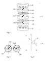
- FIG. 4 illustrates the first and second write magnetic fields 42 and 52 projected along a plane (here, an x-y plane) in which the first and second storage magnetizations 232 and 234 are switchable.
- Hx represents the x-component of the first write magnetic field 42 when projected along the plane
- Hy represents the y-component of the second write magnetic field 52 when projected along the plane.
- a resultant write magnetic field which is represented as H
- ⁇ arctangent (Hy/Hx) when H lies in quadrant I
- ⁇ 180°+arctangent (Hy/Hx) when H lies in quadrant II or III
- ⁇ 360°+arctangent (Hy/Hx) when H lies in quadrant IV.
- FIG. 3 illustrates an example of the first storage magnetization 232 being written in a direction corresponding to a first alignment angle ⁇ 1 , and the second storage magnetization 234 being written in a direction corresponding to a second alignment angle ⁇ 2 .
- FIG. 5 illustrates the magnetic tunnel junction 2 during the TAS-type write operation according to an embodiment and FIG. 6 shows a corresponding chronogram of the write operation.
- the first and second storage magnetization directions 232 and 234 Prior to the write operation, the first and second storage magnetization directions 232 and 234 being oriented in an initial one of m directions ( FIG. 5 a ).
- the first heating current 31 i heat, 1
- the selection transistor 8 is switched to a blocked mode to inhibit current flow through the magnetic tunnel junction 2 , thereby cooling the magnetic tunnel junction 2 to the low threshold temperature T L (see FIGS. 5 d and 6 d ). Either, or both, of the write magnetic fields 42 and 52 can be maintained during cooling of the magnetic tunnel junction 2 , and can be deactivated once the magnetic tunnel junction 2 has cooled at the low threshold temperature T L . Because the first and second storage magnetization directions 232 , 234 are pinned by the exchange bias of the first and second antiferromagnetic layer 24 , 25 , respectively, the switched orientation of the first and second storage magnetization directions 232 , 234 remains stable so as to retain the written data.
- a write operation of the MRAM cell 1 can be carried out by applying a write current through the magnetic tunnel junction 2 via the bit line 3 , using the so-called spin transfer torque (“STT”) effect.
- STT spin transfer torque
- the write current can become spin polarized by passing through a polarizing magnetic layer (not illustrated) or through the sense layer 211 , and a first and second storage magnetization 232 , 234 of the first and second storage layer 231 , 233 , respectively, can be switched according to a spin-polarized orientation of the write current.
- Switching of the first and second storage magnetization 232 , 234 with the spin-polarized write current also can be combined with a TAS-type write operation, such as by heating the magnetic tunnel junction 2 at the first high threshold temperature T H1 and then applying the spin-polarized write current through the magnetic tunnel junction 2 , and heating the magnetic tunnel junction 2 at the second high threshold temperature T H2 and then applying the spin-polarized write current through the magnetic tunnel junction 2 .
- the bit line 3 (functioning as a field line) and the first field line 4 are activated to induce a set of read magnetic fields 44 , 54 to vary a magnetization of the sense layer 211 .
- a first read current 43 can be applied through the first field line 4 to induce a first read magnetic field 44 .
- a second read current 53 can also be applied through the bit line 3 to induce a second read magnetic field 54 .
- the sense magnetization direction 212 is varied in accordance with a resultant read magnetic field corresponding to the combination of the first and second read magnetic fields 44 , 54 .
- the sense magnetization direction 212 can be readily varied under low-intensity magnetic fields and at a temperature that is at the low threshold temperature T L , while the first and second storage magnetization directions 232 , 234 remain stable in their written direction.
- the read operation of the MRAM cell 1 is carried out in multiple read cycles, in which the first and second read magnetic fields 44 , 54 are induced, such that the sense magnetization direction 212 is aligned relative to the switched direction of the first and second storage magnetization 232 , 234 for each read cycle. Because the sense magnetization direction 211 can be aligned according to the resultant read magnetic fields 61 , the sense magnetization direction 211 can be successively switched between m directions according to each read cycle. In such manner, the sense magnetization direction is rotated to m distinct values of ⁇ according to the read operation scheme.
- a degree of alignment between the sense magnetization direction 211 and the first and second storage magnetization directions 232 , 234 is determined by applying a sense current 33 though the magnetic tunnel junction 2 via the bit line 3 , with the selection transistor 8 in a saturated mode. Measuring a resulting voltage across the magnetic tunnel junction 2 when the sense current 33 is applied yields a resistance value R of the magnetic tunnel junction 2 for a particular read cycle, and for a particular alignment of the sense magnetization 211 relative to the orientations of the first and second storage magnetizations 232 , 234 , i.e., for a first angle ⁇ 1 and a second angle ⁇ 2 of the first and second storage magnetizations 232 , 234 , respectively.
- a resistance value can be determined by applying a voltage across the magnetic tunnel junction 2 and measuring a resulting current.
- a resistance value R of the magnetic tunnel junction 2 typically corresponds to a maximum value, namely Rmax, and, when the respective magnetizations are parallel, a resistance value of the magnetic tunnel junction 2 typically corresponds to a minimum value, namely Rmin.
- a resistance value of the magnetic tunnel junction 2 is typically between Rmax and Rmin.
- the read operation further comprises a step of extracting a second local derivative of the resistance response (see FIG. 8 ).
- the read operation further comprises a step of determining a first angle ⁇ 1 corresponding the first direction of the first storage magnetization 232 , and determining a second angle ⁇ 2 corresponding the second direction of the second storage magnetization 234 from the extracted second local derivative.
- determining the first angle ⁇ 1 can be performed by locating a first global minimum M 1 of the extracted second local derivative.
- the local fitting can be performed by using a peak function, such as a Gaussian function.
- a portion of the fitted global minimum peak can then be subtracted around the first global minimum M 1 of the extracted second local derivative, such as to obtain a modified second local derivative.
- the second angle ⁇ 2 can be determined by locating a second global minimum M 2 of the modified second local derivative.
- FIG. 10 shows an example of a modified second local derivative after subtracting a portion of the fitted global minimum peak from the extracted second local derivative.
- the portion of the fitted global minimum peak does correspond to the full fitted global minimum peak. Indeed, in the case the first storage magnetization 232 is parallel to the second storage magnetization 234 , the second angle ⁇ 2 could not be determined.
- the portion comprises about 90% of the fitted global minimum peak.
- the first angle ⁇ 1 and the second angle ⁇ 2 can be stored.
- the read operation can further comprise the step of matching the first angle ⁇ 1 and the second angle ⁇ 2 with a lookup table such as to determine the data written in the MRAM cell 1 .
- the read operation of the MRAM cell 1 explained above is self-referenced, since it can be carried out based on the relative alignment of magnetizations within the MRAM cell 1 , without requiring a comparison to a reference cell or a group of reference cells.
- the self-referenced read implementation of the MRAM cell 1 is particularly desirable when reading multi-bit data, which otherwise would involve a comparison to multiple reference resistance values and would be prone to errors in view of manufacturing variability.
- a faster speed of reading can be achieved by skipping certain of m directions, with a resistance value corresponding to a skipped direction determined by interpolation from adjacent logic states.
- a faster speed of reading also can be achieved by skipping certain of m 2 logic states and using a suitable search technique to locate a minimum resistance value, such as by leveraging symmetries, incremental changes, or curvature related to resistance values of a subset of the m logic states.
- the MRAM cell includes a second field line magnetically coupled to the magnetic tunnel junction 2 .
- the second field line can be located, for example, above the bit line 3 or below the first field line 4 , orthogonal to the first field line 4 .
- a second write current 51 can be applied through the second field line to induce a second write magnetic field to switch a first and/or storage magnetization direction 232 , 234 accordingly.
- a second read current 53 can be applied through the second field line to induce a second read magnetic field 54 to vary a sense magnetization direction 211 accordingly.
- the second field line can be activated in combination with the first field line 4 to induce a resultant magnetic field during writing and reading.
- the bit line 3 can be used only for passing the first and second heating currents 31 , 32 and the sense current 33 , separately from the second write and read currents.
- a memory device implemented in accordance with an embodiment of the invention includes a set of MRAM cells 1 .
- Each of the MRAM cells 1 includes a magnetic tunnel junction 2 and a selection transistor 8 .
- the MRAM cells 1 can be arranged in rows and columns along substantially orthogonal directions of a square or rectangular array, although other two-dimensional and three-dimensional arrays are contemplated.
- the memory device can include a set of bit lines 3 electrically connecting each MRAM cell 1 of the memory device along a row.
- the memory device further includes a set of first field lines 4 magnetically coupled to the magnetic tunnel junction 2 of each MRAM cell 1 along a column of the memory device.
- the memory device can further include a set of control lines, which are electrically coupled to the MRAM cells 1 through the selection transistor 8 along one column of the array. During write and read operations, the control lines switch the selection transistors 8 between a blocked mode (OFF) and a saturated mode (ON).
- OFF blocked mode
- ON saturated mode
- the field lines 4 can be combined into a common field line that is magnetically coupled to, and shared by, the MRAM cells 1 in two adjacent different columns.
- the first field lines 4 can be disposed above the bit lines 3 , rather than below the bit lines 3 .
- a set of second field lines can be included above the bit lines 3 , in addition to the first field lines 4 .
Landscapes
- Engineering & Computer Science (AREA)
- Computer Hardware Design (AREA)
- Mram Or Spin Memory Techniques (AREA)
- Hall/Mr Elements (AREA)
Abstract
Description
- 1 MRAM cell
- 2 magnetic tunnel junction
- 211 magnetic sense layer
- 212 sense magnetization
- 221 first spacer layer
- 222 second spacer layer
- 231 first magnetic storage layer
- 232 first storage magnetization
- 233 second magnetic storage layer
- 234 second storage magnetization
- 24 first antiferromagnetic layer
- 25 second antiferromagnetic layer
- 3 bit line
- 31 first heating current
- 32 second heating current
- 33 sense current
- 4 first field line
- 41 first write current
- 42 first write magnetic field
- 43 first read current
- 44 first read magnetic field
- 5 second field line
- 51 second write current
- 52 second write magnetic field
- 53 second read current
- 54 second read magnetic field
- θ1 first angle
- θ2 second angle
- M1 first global minimum
- M2 second global minimum
- R resistance of the magnetic tunnel junction
- TL low threshold temperature
- TH1 first high threshold temperature
- TH2 second high threshold temperature
Claims (18)
Applications Claiming Priority (4)
| Application Number | Priority Date | Filing Date | Title |
|---|---|---|---|
| EP14290144 | 2014-05-09 | ||
| EP14290144.6A EP2942780B1 (en) | 2014-05-09 | 2014-05-09 | Multi-bit MRAM cell and method for writing and reading to such MRAM cell |
| EP14290144.6 | 2014-05-09 | ||
| PCT/EP2015/058797 WO2015169610A1 (en) | 2014-05-09 | 2015-04-23 | Multi-bit mram cell and method for writing and reading to such mram cell |
Publications (2)
| Publication Number | Publication Date |
|---|---|
| US20170076771A1 US20170076771A1 (en) | 2017-03-16 |
| US9799384B2 true US9799384B2 (en) | 2017-10-24 |
Family
ID=50897500
Family Applications (1)
| Application Number | Title | Priority Date | Filing Date |
|---|---|---|---|
| US15/309,229 Active US9799384B2 (en) | 2014-05-09 | 2015-04-23 | Multi-bit MRAM cell and method for writing and reading to such MRAM cell |
Country Status (3)
| Country | Link |
|---|---|
| US (1) | US9799384B2 (en) |
| EP (1) | EP2942780B1 (en) |
| WO (1) | WO2015169610A1 (en) |
Cited By (1)
| Publication number | Priority date | Publication date | Assignee | Title |
|---|---|---|---|---|
| US11437083B2 (en) | 2021-02-05 | 2022-09-06 | International Business Machines Corporation | Two-bit magnetoresistive random-access memory device architecture |
Families Citing this family (7)
| Publication number | Priority date | Publication date | Assignee | Title |
|---|---|---|---|---|
| US10593396B2 (en) * | 2018-07-06 | 2020-03-17 | Spin Memory, Inc. | Multi-bit cell read-out techniques for MRAM cells with mixed pinned magnetization orientations |
| US10692569B2 (en) | 2018-07-06 | 2020-06-23 | Spin Memory, Inc. | Read-out techniques for multi-bit cells |
| US10559338B2 (en) * | 2018-07-06 | 2020-02-11 | Spin Memory, Inc. | Multi-bit cell read-out techniques |
| US10600478B2 (en) * | 2018-07-06 | 2020-03-24 | Spin Memory, Inc. | Multi-bit cell read-out techniques for MRAM cells with mixed pinned magnetization orientations |
| CN109585644A (en) * | 2018-11-09 | 2019-04-05 | 中国科学院微电子研究所 | Spin(-)orbit torque magnetic random access memory and wiring method, device |
| CN115482853B (en) * | 2022-08-11 | 2026-02-03 | 桂林电子科技大学 | Bit logic operator and electronic device |
| CN117130834B (en) * | 2023-01-30 | 2024-06-14 | 荣耀终端有限公司 | Method for preventing magnetic field from interfering with operation of electronic equipment and electronic equipment |
Citations (5)
| Publication number | Priority date | Publication date | Assignee | Title |
|---|---|---|---|---|
| EP2447949A1 (en) | 2010-10-26 | 2012-05-02 | Crocus Technology | Multi level magnetic element |
| US20120201074A1 (en) | 2011-02-08 | 2012-08-09 | Neal Berger | Magnetic Random Access Memory Devices Configured for Self-Referenced Read Operation |
| US20130070520A1 (en) * | 2011-09-21 | 2013-03-21 | Mourad El Baraji | Magnetic Random Access Memory Devices Including Shared Heating Straps |
| US8411500B2 (en) * | 2010-07-07 | 2013-04-02 | Crocus Technology Sa | Magnetic device with optimized heat confinement |
| WO2014063939A1 (en) | 2012-10-25 | 2014-05-01 | Crocus Technology | Thermally assisted mram cell and method for writing a plurality of bits in the mram cell |
-
2014
- 2014-05-09 EP EP14290144.6A patent/EP2942780B1/en active Active
-
2015
- 2015-04-23 US US15/309,229 patent/US9799384B2/en active Active
- 2015-04-23 WO PCT/EP2015/058797 patent/WO2015169610A1/en not_active Ceased
Patent Citations (5)
| Publication number | Priority date | Publication date | Assignee | Title |
|---|---|---|---|---|
| US8411500B2 (en) * | 2010-07-07 | 2013-04-02 | Crocus Technology Sa | Magnetic device with optimized heat confinement |
| EP2447949A1 (en) | 2010-10-26 | 2012-05-02 | Crocus Technology | Multi level magnetic element |
| US20120201074A1 (en) | 2011-02-08 | 2012-08-09 | Neal Berger | Magnetic Random Access Memory Devices Configured for Self-Referenced Read Operation |
| US20130070520A1 (en) * | 2011-09-21 | 2013-03-21 | Mourad El Baraji | Magnetic Random Access Memory Devices Including Shared Heating Straps |
| WO2014063939A1 (en) | 2012-10-25 | 2014-05-01 | Crocus Technology | Thermally assisted mram cell and method for writing a plurality of bits in the mram cell |
Non-Patent Citations (2)
| Title |
|---|
| International Search Report for PCT/EP2015/058797 dated Apr. 23, 2015. |
| Written Opinion for PCT/EP2015/058797 dated Apr. 23, 2015. |
Cited By (1)
| Publication number | Priority date | Publication date | Assignee | Title |
|---|---|---|---|---|
| US11437083B2 (en) | 2021-02-05 | 2022-09-06 | International Business Machines Corporation | Two-bit magnetoresistive random-access memory device architecture |
Also Published As
| Publication number | Publication date |
|---|---|
| WO2015169610A1 (en) | 2015-11-12 |
| EP2942780A1 (en) | 2015-11-11 |
| EP2942780B1 (en) | 2019-10-30 |
| US20170076771A1 (en) | 2017-03-16 |
Similar Documents
| Publication | Publication Date | Title |
|---|---|---|
| US9799384B2 (en) | Multi-bit MRAM cell and method for writing and reading to such MRAM cell | |
| US9837602B2 (en) | Spin-orbit torque bit design for improved switching efficiency | |
| EP2249350B1 (en) | Magnetic memory with a thermally assisted spin transfer torque writing procedure using a low writing current | |
| US8625336B2 (en) | Memory devices with series-interconnected magnetic random access memory cells | |
| US8503225B2 (en) | Multibit cell with synthetic storage layer | |
| US8576615B2 (en) | Magnetic random access memory devices including multi-bit cells | |
| US9818465B2 (en) | Self-referenced memory device and method using spin-orbit torque for reduced size | |
| EP2725580B1 (en) | Thermally assisted MRAM cell and method for writing a plurality of bits in the MRAM cell | |
| US8488372B2 (en) | Magnetic random access memory devices including multi-bit cells | |
| US20130163318A1 (en) | Self-Referenced MRAM Cell and Method for Writing the Cell Using a Spin Transfer Torque Write Operation | |
| US8467234B2 (en) | Magnetic random access memory devices configured for self-referenced read operation | |
| US9054029B2 (en) | Memory devices with magnetic random access memory (MRAM) cells and associated structures for connecting the MRAM cells | |
| US9679624B2 (en) | Magnetic random access memory (MRAM) cell with low power consumption | |
| US9305628B2 (en) | Self-referenced magnetic random access memory (MRAM) and method for writing to the MRAM cell with increased reliability and reduced power consumption | |
| US9947381B2 (en) | Self-referenced multibit MRAM cell having a synthetic antiferromagnetic storage layer | |
| US10115445B2 (en) | Magnetic memory device that is protected against reading using an external magnetic field and method for operating such magnetic memory device | |
| US9875781B2 (en) | Method for writing to a MRAM device configured for self-referenced read operation with improved reproducibly |
Legal Events
| Date | Code | Title | Description |
|---|---|---|---|
| AS | Assignment |
Owner name: CROCUS TECHNOLOGY SA, FRANCE Free format text: ASSIGNMENT OF ASSIGNORS INTEREST;ASSIGNOR:STAINER, QUENTIN;REEL/FRAME:041180/0505 Effective date: 20170201 |
|
| STCF | Information on status: patent grant |
Free format text: PATENTED CASE |
|
| AS | Assignment |
Owner name: LLC "SBERBANK INVESTMENTS", RUSSIAN FEDERATION Free format text: SECURITY INTEREST;ASSIGNOR:CROCUS TECHNOLOGY, INC.;REEL/FRAME:045938/0810 Effective date: 20180314 |
|
| MAFP | Maintenance fee payment |
Free format text: PAYMENT OF MAINTENANCE FEE, 4TH YR, SMALL ENTITY (ORIGINAL EVENT CODE: M2551); ENTITY STATUS OF PATENT OWNER: SMALL ENTITY Year of fee payment: 4 |
|
| AS | Assignment |
Owner name: CROCUS TECHNOLOGY SA, FRANCE Free format text: CHANGE OF ADDRESS;ASSIGNOR:CROCUS TECHNOLOGY SA;REEL/FRAME:064658/0730 Effective date: 20180529 |
|
| AS | Assignment |
Owner name: CROCUS TECHNOLOGY, INC., FRANCE Free format text: RELEASE BY SECURED PARTY;ASSIGNOR:LLC "SBERBANK INVESTMENTS";REEL/FRAME:064783/0420 Effective date: 20220412 |
|
| AS | Assignment |
Owner name: ALLEGRO MICROSYSTEMS, LLC, NEW HAMPSHIRE Free format text: ASSIGNMENT OF ASSIGNORS INTEREST;ASSIGNOR:CROCUS TECHNOLOGY SA;REEL/FRAME:066350/0729 Effective date: 20240101 Owner name: ALLEGRO MICROSYSTEMS, LLC, NEW HAMPSHIRE Free format text: ASSIGNMENT OF ASSIGNORS INTEREST;ASSIGNOR:CROCUS TECHNOLOGY SA;REEL/FRAME:066350/0669 Effective date: 20240101 |
|
| FEPP | Fee payment procedure |
Free format text: ENTITY STATUS SET TO UNDISCOUNTED (ORIGINAL EVENT CODE: BIG.); ENTITY STATUS OF PATENT OWNER: LARGE ENTITY |
|
| MAFP | Maintenance fee payment |
Free format text: PAYMENT OF MAINTENANCE FEE, 8TH YEAR, LARGE ENTITY (ORIGINAL EVENT CODE: M1552); ENTITY STATUS OF PATENT OWNER: LARGE ENTITY Year of fee payment: 8 |