EP2802005A1 - Semiconductor device and method for manufacturing same - Google Patents
Semiconductor device and method for manufacturing same Download PDFInfo
- Publication number
- EP2802005A1 EP2802005A1 EP12864530.6A EP12864530A EP2802005A1 EP 2802005 A1 EP2802005 A1 EP 2802005A1 EP 12864530 A EP12864530 A EP 12864530A EP 2802005 A1 EP2802005 A1 EP 2802005A1
- Authority
- EP
- European Patent Office
- Prior art keywords
- hole
- semiconductor substrate
- stage
- etching
- shape portion
- Prior art date
- Legal status (The legal status is an assumption and is not a legal conclusion. Google has not performed a legal analysis and makes no representation as to the accuracy of the status listed.)
- Granted
Links
- 239000004065 semiconductor Substances 0.000 title claims abstract description 240
- 238000000034 method Methods 0.000 title claims description 156
- 238000004519 manufacturing process Methods 0.000 title claims description 45
- 239000000758 substrate Substances 0.000 claims abstract description 196
- 229910052751 metal Inorganic materials 0.000 claims abstract description 33
- 239000002184 metal Substances 0.000 claims abstract description 33
- 238000001312 dry etching Methods 0.000 claims description 75
- 229910000679 solder Inorganic materials 0.000 claims description 30
- 238000005229 chemical vapour deposition Methods 0.000 claims description 16
- 239000010410 layer Substances 0.000 description 57
- 238000005530 etching Methods 0.000 description 38
- 229920002120 photoresistant polymer Polymers 0.000 description 35
- 239000011521 glass Substances 0.000 description 25
- 238000010586 diagram Methods 0.000 description 24
- VYPSYNLAJGMNEJ-UHFFFAOYSA-N Silicium dioxide Chemical compound O=[Si]=O VYPSYNLAJGMNEJ-UHFFFAOYSA-N 0.000 description 21
- 238000003384 imaging method Methods 0.000 description 19
- 239000010949 copper Substances 0.000 description 17
- 229910052710 silicon Inorganic materials 0.000 description 17
- 239000010703 silicon Substances 0.000 description 17
- XUIMIQQOPSSXEZ-UHFFFAOYSA-N Silicon Chemical compound [Si] XUIMIQQOPSSXEZ-UHFFFAOYSA-N 0.000 description 15
- 229910052802 copper Inorganic materials 0.000 description 15
- RYGMFSIKBFXOCR-UHFFFAOYSA-N Copper Chemical compound [Cu] RYGMFSIKBFXOCR-UHFFFAOYSA-N 0.000 description 14
- 229910018503 SF6 Inorganic materials 0.000 description 14
- SFZCNBIFKDRMGX-UHFFFAOYSA-N sulfur hexafluoride Chemical compound FS(F)(F)(F)(F)F SFZCNBIFKDRMGX-UHFFFAOYSA-N 0.000 description 14
- 238000001020 plasma etching Methods 0.000 description 10
- 238000004544 sputter deposition Methods 0.000 description 10
- 239000012790 adhesive layer Substances 0.000 description 9
- 230000015572 biosynthetic process Effects 0.000 description 9
- 238000000206 photolithography Methods 0.000 description 8
- 239000000463 material Substances 0.000 description 7
- 238000002161 passivation Methods 0.000 description 7
- 229920005989 resin Polymers 0.000 description 7
- 239000011347 resin Substances 0.000 description 7
- BOTDANWDWHJENH-UHFFFAOYSA-N Tetraethyl orthosilicate Chemical compound CCO[Si](OCC)(OCC)OCC BOTDANWDWHJENH-UHFFFAOYSA-N 0.000 description 6
- 238000010438 heat treatment Methods 0.000 description 6
- 238000005498 polishing Methods 0.000 description 6
- 230000001681 protective effect Effects 0.000 description 6
- 238000009792 diffusion process Methods 0.000 description 5
- 230000002265 prevention Effects 0.000 description 5
- 239000000853 adhesive Substances 0.000 description 4
- 230000001070 adhesive effect Effects 0.000 description 4
- 238000004380 ashing Methods 0.000 description 4
- FFBHFFJDDLITSX-UHFFFAOYSA-N benzyl N-[2-hydroxy-4-(3-oxomorpholin-4-yl)phenyl]carbamate Chemical compound OC1=C(NC(=O)OCC2=CC=CC=C2)C=CC(=C1)N1CCOCC1=O FFBHFFJDDLITSX-UHFFFAOYSA-N 0.000 description 4
- 239000004020 conductor Substances 0.000 description 4
- BCCOBQSFUDVTJQ-UHFFFAOYSA-N octafluorocyclobutane Chemical compound FC1(F)C(F)(F)C(F)(F)C1(F)F BCCOBQSFUDVTJQ-UHFFFAOYSA-N 0.000 description 4
- 235000019407 octafluorocyclobutane Nutrition 0.000 description 4
- 238000005268 plasma chemical vapour deposition Methods 0.000 description 4
- 239000000126 substance Substances 0.000 description 4
- 239000002344 surface layer Substances 0.000 description 4
- 229920001169 thermoplastic Polymers 0.000 description 4
- 239000004416 thermosoftening plastic Substances 0.000 description 4
- 229910052581 Si3N4 Inorganic materials 0.000 description 3
- 238000005520 cutting process Methods 0.000 description 3
- 230000007547 defect Effects 0.000 description 3
- 230000000694 effects Effects 0.000 description 3
- HQVNEWCFYHHQES-UHFFFAOYSA-N silicon nitride Chemical compound N12[Si]34N5[Si]62N3[Si]51N64 HQVNEWCFYHHQES-UHFFFAOYSA-N 0.000 description 3
- 125000006850 spacer group Chemical group 0.000 description 3
- 229960000909 sulfur hexafluoride Drugs 0.000 description 3
- 239000010936 titanium Substances 0.000 description 3
- NRTOMJZYCJJWKI-UHFFFAOYSA-N Titanium nitride Chemical compound [Ti]#N NRTOMJZYCJJWKI-UHFFFAOYSA-N 0.000 description 2
- 229910052782 aluminium Inorganic materials 0.000 description 2
- XAGFODPZIPBFFR-UHFFFAOYSA-N aluminium Chemical compound [Al] XAGFODPZIPBFFR-UHFFFAOYSA-N 0.000 description 2
- 230000001413 cellular effect Effects 0.000 description 2
- 238000007772 electroless plating Methods 0.000 description 2
- 238000002474 experimental method Methods 0.000 description 2
- 238000000227 grinding Methods 0.000 description 2
- 238000007747 plating Methods 0.000 description 2
- 239000010453 quartz Substances 0.000 description 2
- 229910052814 silicon oxide Inorganic materials 0.000 description 2
- 229910052719 titanium Inorganic materials 0.000 description 2
- 239000004593 Epoxy Substances 0.000 description 1
- JOYRKODLDBILNP-UHFFFAOYSA-N Ethyl urethane Chemical compound CCOC(N)=O JOYRKODLDBILNP-UHFFFAOYSA-N 0.000 description 1
- 239000004642 Polyimide Substances 0.000 description 1
- RTAQQCXQSZGOHL-UHFFFAOYSA-N Titanium Chemical compound [Ti] RTAQQCXQSZGOHL-UHFFFAOYSA-N 0.000 description 1
- NIXOWILDQLNWCW-UHFFFAOYSA-N acrylic acid group Chemical group C(C=C)(=O)O NIXOWILDQLNWCW-UHFFFAOYSA-N 0.000 description 1
- 229910045601 alloy Inorganic materials 0.000 description 1
- 239000000956 alloy Substances 0.000 description 1
- 230000000295 complement effect Effects 0.000 description 1
- 239000010432 diamond Substances 0.000 description 1
- 229910003460 diamond Inorganic materials 0.000 description 1
- 230000005684 electric field Effects 0.000 description 1
- 238000010894 electron beam technology Methods 0.000 description 1
- 239000003822 epoxy resin Substances 0.000 description 1
- 230000002452 interceptive effect Effects 0.000 description 1
- 239000011229 interlayer Substances 0.000 description 1
- 238000003475 lamination Methods 0.000 description 1
- 239000007788 liquid Substances 0.000 description 1
- 229910044991 metal oxide Inorganic materials 0.000 description 1
- 150000004706 metal oxides Chemical class 0.000 description 1
- 150000002739 metals Chemical class 0.000 description 1
- 229920003986 novolac Polymers 0.000 description 1
- 229920000647 polyepoxide Polymers 0.000 description 1
- 229920001721 polyimide Polymers 0.000 description 1
- 238000000926 separation method Methods 0.000 description 1
- MZLGASXMSKOWSE-UHFFFAOYSA-N tantalum nitride Chemical compound [Ta]#N MZLGASXMSKOWSE-UHFFFAOYSA-N 0.000 description 1
- 229920001187 thermosetting polymer Polymers 0.000 description 1
- 239000012780 transparent material Substances 0.000 description 1
- 239000011800 void material Substances 0.000 description 1
- 238000001039 wet etching Methods 0.000 description 1
Images


Classifications
-
- H—ELECTRICITY
- H01—ELECTRIC ELEMENTS
- H01L—SEMICONDUCTOR DEVICES NOT COVERED BY CLASS H10
- H01L21/00—Processes or apparatus adapted for the manufacture or treatment of semiconductor or solid state devices or of parts thereof
- H01L21/70—Manufacture or treatment of devices consisting of a plurality of solid state components formed in or on a common substrate or of parts thereof; Manufacture of integrated circuit devices or of parts thereof
- H01L21/71—Manufacture of specific parts of devices defined in group H01L21/70
- H01L21/768—Applying interconnections to be used for carrying current between separate components within a device comprising conductors and dielectrics
- H01L21/76801—Applying interconnections to be used for carrying current between separate components within a device comprising conductors and dielectrics characterised by the formation and the after-treatment of the dielectrics, e.g. smoothing
- H01L21/76802—Applying interconnections to be used for carrying current between separate components within a device comprising conductors and dielectrics characterised by the formation and the after-treatment of the dielectrics, e.g. smoothing by forming openings in dielectrics
- H01L21/76814—Applying interconnections to be used for carrying current between separate components within a device comprising conductors and dielectrics characterised by the formation and the after-treatment of the dielectrics, e.g. smoothing by forming openings in dielectrics post-treatment or after-treatment, e.g. cleaning or removal of oxides on underlying conductors
-
- H—ELECTRICITY
- H01—ELECTRIC ELEMENTS
- H01L—SEMICONDUCTOR DEVICES NOT COVERED BY CLASS H10
- H01L21/00—Processes or apparatus adapted for the manufacture or treatment of semiconductor or solid state devices or of parts thereof
- H01L21/70—Manufacture or treatment of devices consisting of a plurality of solid state components formed in or on a common substrate or of parts thereof; Manufacture of integrated circuit devices or of parts thereof
- H01L21/71—Manufacture of specific parts of devices defined in group H01L21/70
- H01L21/768—Applying interconnections to be used for carrying current between separate components within a device comprising conductors and dielectrics
- H01L21/76898—Applying interconnections to be used for carrying current between separate components within a device comprising conductors and dielectrics formed through a semiconductor substrate
-
- H—ELECTRICITY
- H01—ELECTRIC ELEMENTS
- H01L—SEMICONDUCTOR DEVICES NOT COVERED BY CLASS H10
- H01L21/00—Processes or apparatus adapted for the manufacture or treatment of semiconductor or solid state devices or of parts thereof
- H01L21/02—Manufacture or treatment of semiconductor devices or of parts thereof
- H01L21/04—Manufacture or treatment of semiconductor devices or of parts thereof the devices having at least one potential-jump barrier or surface barrier, e.g. PN junction, depletion layer or carrier concentration layer
- H01L21/18—Manufacture or treatment of semiconductor devices or of parts thereof the devices having at least one potential-jump barrier or surface barrier, e.g. PN junction, depletion layer or carrier concentration layer the devices having semiconductor bodies comprising elements of Group IV of the Periodic System or AIIIBV compounds with or without impurities, e.g. doping materials
- H01L21/30—Treatment of semiconductor bodies using processes or apparatus not provided for in groups H01L21/20 - H01L21/26
- H01L21/302—Treatment of semiconductor bodies using processes or apparatus not provided for in groups H01L21/20 - H01L21/26 to change their surface-physical characteristics or shape, e.g. etching, polishing, cutting
- H01L21/306—Chemical or electrical treatment, e.g. electrolytic etching
- H01L21/3065—Plasma etching; Reactive-ion etching
- H01L21/30655—Plasma etching; Reactive-ion etching comprising alternated and repeated etching and passivation steps, e.g. Bosch process
-
- H—ELECTRICITY
- H01—ELECTRIC ELEMENTS
- H01L—SEMICONDUCTOR DEVICES NOT COVERED BY CLASS H10
- H01L21/00—Processes or apparatus adapted for the manufacture or treatment of semiconductor or solid state devices or of parts thereof
- H01L21/02—Manufacture or treatment of semiconductor devices or of parts thereof
- H01L21/04—Manufacture or treatment of semiconductor devices or of parts thereof the devices having at least one potential-jump barrier or surface barrier, e.g. PN junction, depletion layer or carrier concentration layer
- H01L21/18—Manufacture or treatment of semiconductor devices or of parts thereof the devices having at least one potential-jump barrier or surface barrier, e.g. PN junction, depletion layer or carrier concentration layer the devices having semiconductor bodies comprising elements of Group IV of the Periodic System or AIIIBV compounds with or without impurities, e.g. doping materials
- H01L21/30—Treatment of semiconductor bodies using processes or apparatus not provided for in groups H01L21/20 - H01L21/26
- H01L21/31—Treatment of semiconductor bodies using processes or apparatus not provided for in groups H01L21/20 - H01L21/26 to form insulating layers thereon, e.g. for masking or by using photolithographic techniques; After treatment of these layers; Selection of materials for these layers
- H01L21/3105—After-treatment
- H01L21/311—Etching the insulating layers by chemical or physical means
- H01L21/31105—Etching inorganic layers
- H01L21/31111—Etching inorganic layers by chemical means
- H01L21/31116—Etching inorganic layers by chemical means by dry-etching
-
- H—ELECTRICITY
- H01—ELECTRIC ELEMENTS
- H01L—SEMICONDUCTOR DEVICES NOT COVERED BY CLASS H10
- H01L21/00—Processes or apparatus adapted for the manufacture or treatment of semiconductor or solid state devices or of parts thereof
- H01L21/70—Manufacture or treatment of devices consisting of a plurality of solid state components formed in or on a common substrate or of parts thereof; Manufacture of integrated circuit devices or of parts thereof
- H01L21/71—Manufacture of specific parts of devices defined in group H01L21/70
- H01L21/768—Applying interconnections to be used for carrying current between separate components within a device comprising conductors and dielectrics
- H01L21/76801—Applying interconnections to be used for carrying current between separate components within a device comprising conductors and dielectrics characterised by the formation and the after-treatment of the dielectrics, e.g. smoothing
- H01L21/76802—Applying interconnections to be used for carrying current between separate components within a device comprising conductors and dielectrics characterised by the formation and the after-treatment of the dielectrics, e.g. smoothing by forming openings in dielectrics
- H01L21/76816—Aspects relating to the layout of the pattern or to the size of vias or trenches
-
- H—ELECTRICITY
- H01—ELECTRIC ELEMENTS
- H01L—SEMICONDUCTOR DEVICES NOT COVERED BY CLASS H10
- H01L21/00—Processes or apparatus adapted for the manufacture or treatment of semiconductor or solid state devices or of parts thereof
- H01L21/70—Manufacture or treatment of devices consisting of a plurality of solid state components formed in or on a common substrate or of parts thereof; Manufacture of integrated circuit devices or of parts thereof
- H01L21/71—Manufacture of specific parts of devices defined in group H01L21/70
- H01L21/768—Applying interconnections to be used for carrying current between separate components within a device comprising conductors and dielectrics
- H01L21/76838—Applying interconnections to be used for carrying current between separate components within a device comprising conductors and dielectrics characterised by the formation and the after-treatment of the conductors
- H01L21/76877—Filling of holes, grooves or trenches, e.g. vias, with conductive material
-
- H—ELECTRICITY
- H01—ELECTRIC ELEMENTS
- H01L—SEMICONDUCTOR DEVICES NOT COVERED BY CLASS H10
- H01L23/00—Details of semiconductor or other solid state devices
- H01L23/48—Arrangements for conducting electric current to or from the solid state body in operation, e.g. leads, terminal arrangements ; Selection of materials therefor
- H01L23/481—Internal lead connections, e.g. via connections, feedthrough structures
-
- H—ELECTRICITY
- H01—ELECTRIC ELEMENTS
- H01L—SEMICONDUCTOR DEVICES NOT COVERED BY CLASS H10
- H01L27/00—Devices consisting of a plurality of semiconductor or other solid-state components formed in or on a common substrate
- H01L27/14—Devices consisting of a plurality of semiconductor or other solid-state components formed in or on a common substrate including semiconductor components sensitive to infrared radiation, light, electromagnetic radiation of shorter wavelength or corpuscular radiation and specially adapted either for the conversion of the energy of such radiation into electrical energy or for the control of electrical energy by such radiation
- H01L27/144—Devices controlled by radiation
- H01L27/146—Imager structures
- H01L27/14601—Structural or functional details thereof
- H01L27/14618—Containers
-
- H—ELECTRICITY
- H01—ELECTRIC ELEMENTS
- H01L—SEMICONDUCTOR DEVICES NOT COVERED BY CLASS H10
- H01L27/00—Devices consisting of a plurality of semiconductor or other solid-state components formed in or on a common substrate
- H01L27/14—Devices consisting of a plurality of semiconductor or other solid-state components formed in or on a common substrate including semiconductor components sensitive to infrared radiation, light, electromagnetic radiation of shorter wavelength or corpuscular radiation and specially adapted either for the conversion of the energy of such radiation into electrical energy or for the control of electrical energy by such radiation
- H01L27/144—Devices controlled by radiation
- H01L27/146—Imager structures
- H01L27/14601—Structural or functional details thereof
- H01L27/14636—Interconnect structures
-
- H—ELECTRICITY
- H01—ELECTRIC ELEMENTS
- H01L—SEMICONDUCTOR DEVICES NOT COVERED BY CLASS H10
- H01L27/00—Devices consisting of a plurality of semiconductor or other solid-state components formed in or on a common substrate
- H01L27/14—Devices consisting of a plurality of semiconductor or other solid-state components formed in or on a common substrate including semiconductor components sensitive to infrared radiation, light, electromagnetic radiation of shorter wavelength or corpuscular radiation and specially adapted either for the conversion of the energy of such radiation into electrical energy or for the control of electrical energy by such radiation
- H01L27/144—Devices controlled by radiation
- H01L27/146—Imager structures
- H01L27/14683—Processes or apparatus peculiar to the manufacture or treatment of these devices or parts thereof
-
- H—ELECTRICITY
- H01—ELECTRIC ELEMENTS
- H01L—SEMICONDUCTOR DEVICES NOT COVERED BY CLASS H10
- H01L2224/00—Indexing scheme for arrangements for connecting or disconnecting semiconductor or solid-state bodies and methods related thereto as covered by H01L24/00
- H01L2224/01—Means for bonding being attached to, or being formed on, the surface to be connected, e.g. chip-to-package, die-attach, "first-level" interconnects; Manufacturing methods related thereto
- H01L2224/02—Bonding areas; Manufacturing methods related thereto
- H01L2224/023—Redistribution layers [RDL] for bonding areas
- H01L2224/0237—Disposition of the redistribution layers
- H01L2224/02372—Disposition of the redistribution layers connecting to a via connection in the semiconductor or solid-state body
-
- H—ELECTRICITY
- H01—ELECTRIC ELEMENTS
- H01L—SEMICONDUCTOR DEVICES NOT COVERED BY CLASS H10
- H01L2224/00—Indexing scheme for arrangements for connecting or disconnecting semiconductor or solid-state bodies and methods related thereto as covered by H01L24/00
- H01L2224/01—Means for bonding being attached to, or being formed on, the surface to be connected, e.g. chip-to-package, die-attach, "first-level" interconnects; Manufacturing methods related thereto
- H01L2224/02—Bonding areas; Manufacturing methods related thereto
- H01L2224/04—Structure, shape, material or disposition of the bonding areas prior to the connecting process
- H01L2224/0401—Bonding areas specifically adapted for bump connectors, e.g. under bump metallisation [UBM]
-
- H—ELECTRICITY
- H01—ELECTRIC ELEMENTS
- H01L—SEMICONDUCTOR DEVICES NOT COVERED BY CLASS H10
- H01L2224/00—Indexing scheme for arrangements for connecting or disconnecting semiconductor or solid-state bodies and methods related thereto as covered by H01L24/00
- H01L2224/01—Means for bonding being attached to, or being formed on, the surface to be connected, e.g. chip-to-package, die-attach, "first-level" interconnects; Manufacturing methods related thereto
- H01L2224/02—Bonding areas; Manufacturing methods related thereto
- H01L2224/04—Structure, shape, material or disposition of the bonding areas prior to the connecting process
- H01L2224/05—Structure, shape, material or disposition of the bonding areas prior to the connecting process of an individual bonding area
- H01L2224/0554—External layer
- H01L2224/05541—Structure
- H01L2224/05548—Bonding area integrally formed with a redistribution layer on the semiconductor or solid-state body
-
- H—ELECTRICITY
- H01—ELECTRIC ELEMENTS
- H01L—SEMICONDUCTOR DEVICES NOT COVERED BY CLASS H10
- H01L2224/00—Indexing scheme for arrangements for connecting or disconnecting semiconductor or solid-state bodies and methods related thereto as covered by H01L24/00
- H01L2224/01—Means for bonding being attached to, or being formed on, the surface to be connected, e.g. chip-to-package, die-attach, "first-level" interconnects; Manufacturing methods related thereto
- H01L2224/10—Bump connectors; Manufacturing methods related thereto
- H01L2224/12—Structure, shape, material or disposition of the bump connectors prior to the connecting process
- H01L2224/13—Structure, shape, material or disposition of the bump connectors prior to the connecting process of an individual bump connector
- H01L2224/13001—Core members of the bump connector
- H01L2224/1302—Disposition
- H01L2224/13022—Disposition the bump connector being at least partially embedded in the surface
-
- H—ELECTRICITY
- H01—ELECTRIC ELEMENTS
- H01L—SEMICONDUCTOR DEVICES NOT COVERED BY CLASS H10
- H01L2224/00—Indexing scheme for arrangements for connecting or disconnecting semiconductor or solid-state bodies and methods related thereto as covered by H01L24/00
- H01L2224/01—Means for bonding being attached to, or being formed on, the surface to be connected, e.g. chip-to-package, die-attach, "first-level" interconnects; Manufacturing methods related thereto
- H01L2224/10—Bump connectors; Manufacturing methods related thereto
- H01L2224/12—Structure, shape, material or disposition of the bump connectors prior to the connecting process
- H01L2224/13—Structure, shape, material or disposition of the bump connectors prior to the connecting process of an individual bump connector
- H01L2224/13001—Core members of the bump connector
- H01L2224/1302—Disposition
- H01L2224/13024—Disposition the bump connector being disposed on a redistribution layer on the semiconductor or solid-state body
-
- H—ELECTRICITY
- H01—ELECTRIC ELEMENTS
- H01L—SEMICONDUCTOR DEVICES NOT COVERED BY CLASS H10
- H01L2224/00—Indexing scheme for arrangements for connecting or disconnecting semiconductor or solid-state bodies and methods related thereto as covered by H01L24/00
- H01L2224/01—Means for bonding being attached to, or being formed on, the surface to be connected, e.g. chip-to-package, die-attach, "first-level" interconnects; Manufacturing methods related thereto
- H01L2224/10—Bump connectors; Manufacturing methods related thereto
- H01L2224/12—Structure, shape, material or disposition of the bump connectors prior to the connecting process
- H01L2224/13—Structure, shape, material or disposition of the bump connectors prior to the connecting process of an individual bump connector
- H01L2224/13001—Core members of the bump connector
- H01L2224/13099—Material
- H01L2224/131—Material with a principal constituent of the material being a metal or a metalloid, e.g. boron [B], silicon [Si], germanium [Ge], arsenic [As], antimony [Sb], tellurium [Te] and polonium [Po], and alloys thereof
-
- H—ELECTRICITY
- H01—ELECTRIC ELEMENTS
- H01L—SEMICONDUCTOR DEVICES NOT COVERED BY CLASS H10
- H01L23/00—Details of semiconductor or other solid state devices
- H01L23/52—Arrangements for conducting electric current within the device in operation from one component to another, i.e. interconnections, e.g. wires, lead frames
- H01L23/522—Arrangements for conducting electric current within the device in operation from one component to another, i.e. interconnections, e.g. wires, lead frames including external interconnections consisting of a multilayer structure of conductive and insulating layers inseparably formed on the semiconductor body
- H01L23/525—Arrangements for conducting electric current within the device in operation from one component to another, i.e. interconnections, e.g. wires, lead frames including external interconnections consisting of a multilayer structure of conductive and insulating layers inseparably formed on the semiconductor body with adaptable interconnections
Definitions
- the present invention relates to a semiconductor device which can be manufactured at low cost and which includes a through-electrode having high connection reliability, and a method for manufacturing the same.
- a solid-state imaging device including a semiconductor device such as a CCD or a CMOS
- camera functions associated with cellular phones a camera module constituted by a solid-state imaging device and a lens system has been built into cellular phones.
- a high-resolution solid-state imaging device which is small-sized, lightweight, and thin is required for these applications. Consequently, in order to realize a pixel count resolution of, for example, 10 million pixels using a small-sized solid-state imaging element, a fine pixel having a size of approximately several ⁇ m square has been manufactured.
- a solid-state imaging device has been manufactured as follows (see Patent Document 1). First, a solid-state imaging element of an integrated circuit and a circuit pattern of an integrated circuit are created on the surface of a semiconductor substrate such as a silicon substrate by a single-sided exposure process. A glass substrate 20 is bonded to the surface of the semiconductor substrate, the thickness of the semiconductor substrate is reduced by polishing the substrate from the back surface thereof, and a through-hole (through-silicon via: hereinafter, abbreviated as a TSV) is processed on the semiconductor substrate.
- a through-hole through-silicon via: hereinafter, abbreviated as a TSV
- a conductive substance is formed on the inner wall of the TSV to form a through-electrode, and an electrical signal of image information obtained in a solid-state imaging element formed on the surface of the semiconductor substrate is sent to the back surface of the semiconductor substrate through the through-electrode.
- Electrical connection to an external circuit can be performed through a connection terminal 16 of a BGA (Ball Grid Array) formed on the back surface of the semiconductor substrate.
- a single-sided exposure process of an element-forming surface is used for forming a semiconductor element on a semiconductor substrate such as a silicon substrate.
- a through-electrode in which a conductor layer is formed on the wall surface of a through-hole with an insulating film interposed therebetween is required for performing multi-layer lamination on a semiconductor chip.
- the through-hole is normally formed by a dry-etching method using plasma.
- the etching depth is several times or more that in a normal semiconductor process, for example, 20 to 500 ⁇ m, the etching time also increases. For this reason, plasma exerts an influence on the semiconductor element formed on the semiconductor substrate. Exposure to plasma for a long period of time causes a rise in the temperature of the surface of the semiconductor substrate, or the occurrence of a defect in the semiconductor element due to an electric field of the plasma.
- CMP chemical mechanical polishing
- Patent Document 2 the following processes are described.
- the present invention is contrived in view of the problems described above, and is to provide a semiconductor device including a through-electrode which is capable of being manufactured by a low-cost manufacturing method, and has high quality and high reliability.
- a semiconductor device to which the present invention is applied is not limited to a package in which an integrated circuit element (IC-chip) is connected to an external circuit in a state where the element is sealed and held.
- the semiconductor device can also be applied to a printed substrate (for example, an interposer) in which a bare chip is mounted onto the upper surface and a terminal is included at the lower surface.
- a semiconductor device including: a semiconductor substrate having a first surface in which an integrated circuit and an I/O pad electrically connected to the integrated circuit are formed, and a second surface which is an opposite side to the first surface; a two-stage through-hole formed in the semiconductor substrate, including a first shape portion having a tapered shape which has a wall surface and of which a diameter of an opening becomes smaller toward a bottom of the hole from the second surface side to a predetermined position of the semiconductor substrate in a thickness direction, and including a second shape portion having a cylindrical shape which extends from the first shape portion to the I/O pad on the first surface side; an inorganic insulating film which is formed on the wall surface of the two-stage through-hole and the second surface; a through-electrode of a metal layer which is formed on the I/O pad and the wall surface of the two-stage through-hole; and a wiring pattern formed on the second surface and connected to the through-electrode.
- a depth of the second shape portion is equal to or less than four times a diameter of the second shape portion.
- the first shape portion includes a tapered wall surface, and in a cross-section of the first shape portion, the tapered wall surface has a tilt with respect to the second surface which is equal to or greater than 60 degrees and equal to or less than 80 degrees.
- the semiconductor device further includes a solder resist protecting the second surface and filled into the first shape portion.
- a method for manufacturing a semiconductor device including: forming an integrated circuit and an I/O pad electrically connected to the integrated circuit on a first surface side of a semiconductor substrate; forming a pattern of a resist for dry-etching having an opening on a second surface side which is an opposite side to the first surface; forming a first shape portion opened from the second surface side to a predetermined position of the semiconductor substrate in a thickness direction so that a diameter of an opening of the first shape portion in the second surface side is larger than a diameter of an opening of the resist for dry-etching and the first shape portion is formed in a tapered shape of which a hole diameter of the first shape portion becomes smaller toward a bottom of the first shape portion, by dry-etching the semiconductor substrate in an RIE mode using a dry-etching apparatus using the resist for dry-etching as a mask; forming a second shape portion including a cylindrical wall surface with the same diameter as that of the opening of the resist for dry-etching which extends
- the method for manufacturing a semiconductor device further includes forming a solder resist for protecting the second surface, and filling the solder resist in the first shape portion.
- the two-stage through-hole constituted by the first shape portion having a tapered shape and the second shape portion having a perpendicular cylindrical wall surface is formed in the semiconductor substrate, thereby allowing a uniform high-quality inorganic insulating film to be formed in the wall surface and bottom of the two-stage through-hole using a chemical vapor deposition method.
- the through-electrode of a uniform and high-quality metal film can be formed on the I/O pad and the wall surface of the two-stage through-hole. Therefore, a semiconductor device is obtained which is capable of being manufactured by a low-cost manufacturing method and in which a through-electrode having good quality and high reliability is formed.
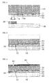
- Fig. 1 is a schematic cross-sectional view illustrating a schematic structure of a semiconductor device 100 according to the present embodiment.
- Fig. 1 shows a cross-sectional view of the semiconductor device 100 cut off along a plane perpendicular to the surface of a semiconductor substrate 10.
- the semiconductor device 100 includes the semiconductor substrate 10 having an integrated circuit 11 of a solid-state imaging element formed therein, a glass substrate 20 arranged at a light-receiving surface (hereinafter, referred to as the first surface) side of the solid-state imaging element of the integrated circuit 11 formed in the semiconductor substrate 10, and a cavity dam 30 which is a spacer for forming a predetermined space (cavity 32) between the semiconductor device 100 and the glass substrate 20.
- a solder ball is mounted as an external connection terminal 40 on the surface (hereinafter, referred to as the second surface) on the opposite side to the surface on which the integrated circuit 11 in the semiconductor substrate 10 is formed.
- the semiconductor substrate 10 for example, using a silicon (111) substrate as a semiconductor substrate 10A, the semiconductor substrate 10 is used in which the thickness of the semiconductor substrate 10A is reduced to equal to or less than 100 ⁇ m.
- the integrated circuit 11 formed on the first surface side of the semiconductor substrate 10 is the integrated circuit 11 in which a solid-state imaging element such as, for example, a CMOS (Complementary Metal Oxide Semiconductor) sensor, a CCD (Charge Coupled Device) sensor, or a photodiode is formed.
- An I/O pad 12 is formed on the first surface side of the semiconductor substrate 10 using a portion of patterns of wirings 12a in the integrated circuit 11 which are formed on an insulating layer 12b.
- a two-stage through-hole 13 which penetrates from the second surface side to the first surface to reach the I/O pad 12 is formed in the semiconductor substrate 10.
- An insulating film 14 is formed on the sidewall of the two-stage through-hole 13, and a through-electrode 15 formed of a metal is formed on the wall surface of the insulating film 14.
- the through-electrode 15 electrically connects the I/O pad 12 and a wiring pattern 41 on the second surface of the semiconductor substrate 10. That is, in the through-electrode 15, the wiring of the semiconductor substrate 10 is extracted from the I/O pad 12 to the wiring pattern 41 on the second surface side.
- solder resist 42 of an insulating resin for protecting the second surface side having the wiring pattern 41 of the semiconductor substrate 10 formed thereon is formed.
- the external connection terminal 40 is formed by forming a solder ball on the wiring pattern 41 exposed to an opening 43 of the solder resist 42.
- the two-stage through-hole 13 of the semiconductor substrate 10 has a first hole (first shape portion) 13a which has a wide opening portion at the second surface side and of which the hole diameter becomes smaller in a tapered shape.
- the first hole 13a is tapered in shape, and thus has the effect of being capable of filling the entirety of the first hole 13a with the solder resist 42.
- the integrated circuit 11 When the integrated circuit 11 is formed by, for example, a CMOS sensor or a photodiode, the integrated circuit 11 has a configuration in which a plurality of pixels of one solid-state imaging element constituted by a semiconductor element such as a CMOS sensor or a photodiode are arranged in a two-dimensional array on the first surface of the semiconductor substrate 10.
- a color filter layer 50 including a RGB color filter corresponding to each pixel and a passivation layer is formed in a region in which pixels of the solid-state imaging element of the integrated circuit 11 formed on the first surface side of the semiconductor substrate 10 are formed.
- a light-shielding film that covers a region in which the solid-state imaging element of the integrated circuit 11 in the first surface of the semiconductor substrate 10 is not formed can also be formed in the portion of the color filter layer 50.
- a condensing micro-lens array 51 can also be formed at a place corresponding to each solid-state imaging element of the integrated circuit 11, on the surface of the color filter layer 50.
- the cavity dam 30 serving as a spacer surrounding the peripheries of the color filter layer 50 and the micro-lens array 51 on the semiconductor substrate 10 is formed on the transparent glass substrate 20.
- the cavity dam 30 of the glass substrate 20 is bonded to the first surface of the semiconductor substrate 10. That is, the lower side of the micro-lens array 51 on the first surface of the semiconductor substrate 10 is covered with the transparent glass substrate 20, and the lateral side of the micro-lens array 51 is covered with the cavity dam 30.
- the integrated circuit 11 of the semiconductor substrate 10, the color filter layer 50, and the cavity 32 in which all directions of the micro-lens array 51 are blocked by the glass substrate 20 and the cavity dam 30 are formed.
- the I/O pad 12 is formed on the first surface side of the semiconductor substrate 10 using a portion of the wirings 12a of the integrated circuit 11.
- the wiring 12a of the integrated circuit 11 including a pattern of the I/O pad 12 can be formed of, for example, aluminum (Al) film.
- Al aluminum
- the wiring 12a of the integrated circuit 11 is not limited thereto, but various electric conductor films such as a copper (Cu) film, a titanium (Ti) film, other metal films, an alloy film, or a laminated film thereof can be used therefor.
- wirings are extracted by the through-electrode 15 from the I/O pad 12 formed by a portion of patterns of wirings 12a of the integrated circuit 11 formed on the first surface of the semiconductor substrate 10 to the second surface side of the semiconductor substrate 10.
- the wiring of the through-electrode 15 is connected to the wiring pattern 41 and the external connection terminal 40 which are formed on the second surface of the semiconductor substrate 10.
- the through-electrode 15 is formed using the two-stage through-hole 13 (also referred to as a contact hole) which penetrates the semiconductor substrate 10 from the second surface side to reach the I/O pad 12 on the first surface. That is, the insulating film 14 is formed on the wall surface of the two-stage through-hole 13, and the through-electrode 15 is formed of a metal film on the insulating film 14.
- the insulating film 14 formed on the wall surface within the two-stage through-hole 13 prevents the through-electrode 15 and the semiconductor substrate 10 from being directly in contact with each other.
- the insulating film 14 also extends onto the second surface of the semiconductor substrate 10, and has the wiring pattern 41 on the second surface side formed thereon, to thereby prevent the wiring pattern 41 and the semiconductor substrate 10 from being directly in contact with each other.
- the through-electrode 15 is electrically connected to the I/O pad 17 exposed to the bottom of the two-stage through-hole 13.
- the through-electrode 15 and the wiring pattern 41 are formed of a conductive layer of the same metal.
- the conductive layer for forming the through-electrode 15 and the wiring pattern 41 can also be formed of, for example, an A1 film, or, can also be formed of a Cu film using a laminated film of Ti and Cu as an underlying layer.
- the thickness of the conductive layer may be, for example, approximately 5 ⁇ m.
- the insulating solder resist 42 is formed on the second surface side of the semiconductor substrate 10 having the wiring pattern 41 formed thereon.
- the solder resist 42 can be formed using, for example, a photosensitive epoxy-based insulating resin.
- the opening 43 in which a solder ball of the external connection terminal 40 is selectively mounted is formed in the solder resist 42.
- the external connection terminal 40 is formed in the opening 43 by self-aligning liquid solder to mount a solder ball.
- the solder resist 42 protects the semiconductor substrate 10 from heat.
- the first hole 13a having a tapered shape opened to the second surface side of the two-stage through-hole 13 is filled with the solder resist 42.
- the filling portion of the solder resist 42 serves as an anchor and thus the solder resist 42 can be tightly fixed to the second surface. Therefore, it is possible to increase the reliability of adhesion to the second surface of the solder resist 42.
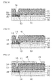
- Figs. 2 to 13 are process diagrams illustrating a method for manufacturing the semiconductor device 100 according to the present embodiment.
- a so-called W-CSP Wafer Level Chip Size Package
- W-CSP Wafer Level Chip Size Package
- the integrated circuit 11 constituted by a large number of solid-state imaging elements is formed on the surface (first surface) of the semiconductor substrate 10A of a silicon wafer having a diameter of 20 cm, 30 cm, or other sizes.
- the I/O pad 12 is formed using a portion of patterns of the wirings 12a formed on the insulating layer 12b of the integrated circuit 11.
- the color filter layer 50 for color separation and the condensing micro-lens array 51 are sequentially formed on the solid-state imaging element on the first surface in association with each pixel.
- the I/O pad 12 of a portion of the wirings 12a of the integrated circuit 11 on the first surface of the semiconductor substrate 10A in Fig. 2 is a basic conductor pattern for forming the through-electrode 15 on the I/O pad 12.
- the cavity dam 30 serving as a spacer surrounding the peripheries of the color filter layer 50 and the micro-lens array 51 on the semiconductor substrate 10A is formed on the transparent glass substrate 20.
- Materials of the cavity dam 30 to be used may include thermosetting polyimide, an epoxy resin, or an acrylic urethane-based photosensitive resin which is used as a resin film with high adhesion.
- the cavity dam 30 having a thickness of approximately 50 to 100 ⁇ m is formed on the glass substrate 20 by a photolithography method having an exposure and development process after a photosensitive resin is applied to the glass substrate 20, as shown in Fig. 3 , with desired patterns located at positions surrounding the color filter and the micro-lens on the semiconductor substrate 10.
- the cavity dam 30 is bonded to the first surface of the semiconductor substrate 10, and the lower side of the micro-lens array 51 on the first surface of the semiconductor substrate 10 is covered with the transparent glass substrate 20.
- the cavity 32 is formed in which all directions are blocked by the semiconductor substrate 10, the glass substrate 20 and the cavity dam 30.
- a void of the cavity 32 is secured between the glass substrate 20 thereof, and the micro-lens array 51, and thus the light-condensing effect of each micro-lens can be prevented from being damaged.
- the thickness of the semiconductor substrate 10A is reduced from the second surface side. This can be performed by combining, for example, grinding, CMP (chemical mechanical polishing), and wet etching as necessary.
- the film thickness of the semiconductor substrate 10 after a reduction in thickness be set to be approximately equal to or less than 50 to 100 ⁇ m. Thereby, a further reduction in size and a further reduction in thickness can be made while maintaining the rigidity of the semiconductor device 100.
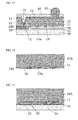
- a photoresist 60 for dry-etching having a thickness of 10 ⁇ m is formed on the second surface of the semiconductor substrate 10 of which the thickness is reduced and has a thickness, of for example, 100 ⁇ m using photolithography.
- a novolac positive-type photosensitive photoresist 60 for dry-etching is applied to the surface of the semiconductor substrate 10 by a spin coater so as to have finally a thickness of 10 ⁇ m, and heated (130°C) and dried by an oven.
- the photoresist 60 for dry-etching is exposed and developed by an exposure apparatus, and thus a pattern having an opening 61 with a diameter of 20 ⁇ m is formed in a region in which the two-stage through-hole 13 located at a position corresponding to the I/O pad 12 is formed.
- the semiconductor substrate 10 is dry-etched by a dry-etching apparatus for five minutes in an RIE (Reactive Ion Etching) mode from the second surface side, using the photoresist 60 for dry-etching as a mask.
- a mixed gas of O 2 which contains SF 6 (sulfur hexafluoride) gas as a main component
- the first hole 13a having a depth of 50 ⁇ m is formed in the second surface side of the semiconductor substrate 10, the hole having an opening with a diameter of 50 ⁇ m which is larger than the diameter of the opening 61 under the opening 61 with a diameter of 20 ⁇ m of the photoresist 60 for dry-etching, and having a tapered shape with a smaller diameter toward the first surface side.
- dry-etching of a Bosch mode is performed in which etching using SF 6 and the protective film formation of the sidewall using C 4 F 8 (perfluorocyclobutane) are alternately performed.
- the dry-etching of a Bosch mode is performed until reaching the I/O pad 12 by alternately repeating an etching step of 6 seconds and a passivation step of 2 seconds of forming a protective film at a coil voltage of 2,500 W.
- a second hole (second shape portion) 13b having a depth of 50 ⁇ m, extending from the bottom of the first hole 13a having a tapered shape which is formed in advance through the semiconductor substrate 10 and the insulating layer 12b to the I/O pad 12 on the first surface side is formed by the dry-etching of a Bosch mode.
- the second hole 13b is formed so as to have a perpendicular cylindrical wall surface with a diameter of 20 ⁇ m of the same size as the diameter of the opening 61 of the photoresist 60 for dry-etching.
- the first hole 13a is first formed which has an opening diameter of 50 ⁇ m from the second surface side of the semiconductor substrate 10, and of which the diameter becomes smaller in a tapered shape from the second surface side to the first surface side.
- the second hole 13b is formed which has a perpendicular cylindrical wall surface with a diameter of 20 ⁇ m extending from the bottom of the first hole 13a to the I/O pad 12.
- the two-stage through-hole 13 is formed which is constituted by the first hole 13a and the second hole 13b passing through the semiconductor substrate 10 having a thickness of 100 ⁇ m to reach the I/O pad 12.
- the cross-sectional shape of the two-stage through-hole 13 is formed to have a wine glass (or cocktail glass) shape.
- the upper portion of the two-stage through-hole 13 is constituted by the first hole 13a of which the diameter becomes smaller in a tapered shape as the wall surface goes from the top to the bottom in a tapered shape.
- This tapered wall surface is suitable for a film forming process of an insulating film 14A in the two-stage through-hole 13 and a film forming process of the through-electrode 15 on the insulating film 14A.
- the wall surface of the second hole 13b extending from the bottom of the first hole 13a of the two-stage through-hole 13 to the underlying I/O pad 12 has a perpendicular cylinder shape and is constant in hole diameter. Even when the thickness of the semiconductor substrate 10 changes, the opening diameter of a hole located below the two-stage through-hole 13 is the same as the hole diameter of the second hole 13b.
- Such a structure is suitable for a film forming process of the stable insulating film 14A in the wall surface extending from the bottom of the first hole 13a of the two-stage through-hole 13 to the I/O pad 12 and a film forming process of the through-electrode 15 on the insulating film 14A.
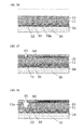
- the photoresist 60 for dry-etching on the surface layer is peeled off by an ashing apparatus using O 2 gas.
- the insulating film 14A is formed on the second surface of the silicon semiconductor substrate 10 and the wall surface of the two-stage through-hole 13.
- the insulating film 14A is formed of an inorganic insulating film such as a silicon oxide film (SiO 2 ) or a silicon nitride film (SiN).
- the insulating film 14A can be formed using CVD (Chemical Vapor Deposition) or the like.
- CVD Chemical Vapor Deposition
- the insulating film 14A of SiO 2 can be formed using ethyl orthosilicate Si(OC 2 H 5 ) 4 , TEOS (Tetraethoxysilane) or the like as a material gas.
- the uniform insulating film 14A was formed up to the wall surface of the two-stage through-hole 13 and the bottom of the two-stage through-hole 13.
- the reason for being able to form a uniform high-quality film is that the two-stage through-hole 13 is a complex of the first hole 13a having a tapered shape and the second hole 13b having a perpendicular cylindrical wall surface.
- the insulating film 14A of SiO 2 in the vicinity of the opening of the first hole 13a of the two-stage through-hole 13 had a film thickness of 1.5 ⁇ m.
- the insulating film 14A having a thickness of 0.6 ⁇ m was formed on the perpendicular cylindrical wall surface of the second hole 13b of the two-stage through-hole 13 which is not likely to form a film.
- the insulating film 14A having a thickness of 0.5 ⁇ m was formed on the I/O pad 12 located below the second hole 13b of the two-stage through-hole 13.
- a resist mask is not used, and etching is performed over the entire surface of the semiconductor substrate 10 by a dry-etching apparatus for an oxide film, using a mixed gas of C 4 F 8 gas which contains SF 6 gas as a main component. The etching is performed until the SiO 2 film of 0.5 ⁇ m located below the two-stage through-hole 13 is removed and the I/O pad 12 located below the hole is exposed.
- the insulating film 14 having a thickness of 0.5 ⁇ m was left on the perpendicular cylindrical wall surface of the second hole 13b of the two-stage through-hole 13.
- the insulating film 14 having a thickness of 0.7 ⁇ m was left in the vicinity of the opening of the first hole 13a of the two-stage through-hole 13, and the insulating film 14 having a thickness of 0.7 ⁇ m was also left on the upper surface of the semiconductor substrate 10.
- the insulating film 14 can be left on the sidewall of the two-stage through-hole 13, and the insulating film 14 can also be left on the second surface of the semiconductor substrate 10.
- the insulating film 14A is removed by dry-etching so as to expose only the I/O pad 12 located below the two-stage through-hole 13, and thus the insulating film 14 can be left on the wall surface of the two-stage through-hole 13 and the second surface of the semiconductor substrate 10 except for that.
- the two-stage through-hole 13 is formed of a complex of the first hole 13 a having a tapered shape and the second hole 13b having a perpendicular cylindrical wall surface, and thus it is possible to form a structure obtained by exposing the I/O pad 12 located below the two-stage through-hole 13 from the insulating film 14 through a low-cost method using an overall etching process of the insulating film 14A in which a resist mask is not used.
- the reason for being able to expose the I/O pad 12 located below of the two-stage through-hole 13 from the insulating film 14 through a low-cost method using an overall etching process of the insulating film 14A in which a resist mask is not used is because the first hole 13a having a tapered shape and the second hole having a perpendicular cylindrical shape which constitute the two-stage through-hole 13 have the following configurations.
- the second hole 13b constituting the two-stage through-hole 13 has a perpendicular cylindrical shape with a diameter of approximately 20 ⁇ m. However, the depth thereof is equal to or less than four times the diameter (the depth of the second hole 13b is equal to or less than 70 ⁇ m when the diameter of the second hole 13b is 18 ⁇ m) and is relatively small. Therefore, when the insulating film 14A is formed by a chemical vapor deposition method in Process 9, the uniform insulating film 14A is formed on the wall surface of the second hole 13b, with a relative large thickness.
- a material gas in a chemical vapor deposition method for forming the insulating film 14A circulates freely without interfering with the inside of the first hole 13a, thereby allowing the gas to reach the second hole 13b.
- the tapered wall surface have a tilt to the second surface of equal to or greater than 60 degrees.
- the reason is because it is preferable that the diameter of the opening of the first hole be made to be smaller than (diameter of the bottom of the first hole 13a) + (half of the thickness of the semiconductor substrate 10), and that the diameter of the opening of the through-electrode 15 be made to be smaller than the thickness of the semiconductor substrate 10.
- the tapered wall surface in the cross-section of the through-hole 13 (or first hole 13a), have a tilt to the second surface which is equal to or greater than 60 degrees and equal to or less than 80 degrees (tilt to the axis of the through-hole 13 is equal to or greater than 10 degrees and equal to or less than 30 degrees).
- the tilt of the tapered wall surface can be controlled by adjusting process conditions of etching of the semiconductor substrate 10.
- the through-electrode 15 is a through-silicon via (TSV) for electrical conduction between the surface and the back surface of the semiconductor substrate 10 which is a silicon substrate.
- TSV through-silicon via
- the thickness of the A1 layer in the vicinity of the opening located at the upper end of the two-stage through-hole 13 was 6 ⁇ m, and a metal layer of A1 was able to be formed which has a thickness of 0.2 ⁇ m on the perpendicular cylindrical wall surface of the second hole 13b located below the two-stage through-hole 13 which is not most likely to allow attachment of a film, and has a thickness of 0.3 ⁇ m on the I/O pad 12 located below the two-stage through-hole 13.
- the two-stage through-hole 13 is formed of a complex of the first hole 13a having a tapered shape and the second hole 13b having a perpendicular cylindrical wall surface, thereby allowing the uniform high-quality through-electrode 15 to be formed on the inner wall surface of the two-stage through-hole 13 by a vacuum film formation method.
- the metal layer in order to form a metal layer, even when a vacuum film formation method of a CVD method is used without being limited to a sputtering method, the metal layer can be formed satisfactorily without the occurrence of a defect on the wall surface of the two-stage through-hole 13.
- a photoresist is formed on a metal layer that covers the second surface side of the semiconductor substrate 10 by photolithography.
- the wiring pattern 41 is formed on the second surface of the semiconductor substrate 10 by etching and removing patterns other than the metal layer protected by this photoresist.
- a solution of a solder resist is applied to the second surface side of the semiconductor substrate 10 on which the wiring pattern 41 is formed.
- the solder resist is dried, and is next patterned by a photolithography process and an etching process. Thereby, as shown in Fig. 12 , the solder resist 42 having the opening 43 formed therein is formed in a place for mounting a solder ball of the external connection terminal 40.
- the first hole 13 a which has a wide opening portion and of which the hole diameter becomes smaller in a tapered shape is formed at the second surface side of the semiconductor substrate 10. Since the shape thereof is tapered, the entirety of the first hole 13a can be filled with the solder resist 42.
- a solder ball is mounted on a wiring pattern exposed to the opening 43 of the solder resist 42 to form the external connection terminal 40.
- the semiconductor substrate 10 is diced along a scribe region using, for example, a diamond cutter or a laser beam. Thereby, the semiconductor device 100 formed in a two-dimensional array on the semiconductor substrate 10 of silicon is fragmented.
- the two-stage through-hole 13 constituted by the first hole 13a having a tapered shape extending from the second surface to the I/O pad 12 on the first surface and the second hole 13b having a cylindrical wall surface is formed in the semiconductor substrate 10 having the integrated circuit 11 as a semiconductor element formed on the first surface.
- the high-quality insulating film 14 and the high-quality through-electrode 15 (TSV) having a metal layer can be formed in the two-stage through-hole 13. Therefore, the semiconductor device 100 is obtained in which the wiring of the integrated circuit 11 and the wiring pattern 41 on the second surface side are electrically connected to each other through the high-quality through-electrode 15.
- the first hole 13a and the second hole 13b may not necessarily be formed to have the same depth.
- the first hole 13a may be formed up to a predetermined position of the semiconductor substrate 10 in a thickness direction, and the second hole 13b may be formed thereunder.
- a second embodiment is different from the first embodiment in that a semiconductor device except for a solid-state imaging device is manufactured.
- the through-electrode 15 (TSV) and wiring pattern 41 are formed in a metal layer using copper.
- the integrated circuit 11 is formed on the surface of the semiconductor substrate 10A of a silicon wafer, and the I/O pad 12 is formed using a portion of the wirings 12a formed on the insulating layer 12b of the integrated circuit 11.
- a support substrate 12 is attached to the semiconductor substrate 10A to form an integral structure.
- the semiconductor substrate 10A is easily handled, and the thickness of the semiconductor substrate 10A is reduced to approximately 10 ⁇ m to 50 ⁇ m.
- a passivation film 33 such as a silicon nitride film is first formed which covers the integrated circuit 11 and the I/O pad 12 on the surface of the semiconductor substrate 10A of silicon. Further, an adhesive layer 34 is applied onto the passivation film 33, and the support substrate 12 is bonded to the semiconductor substrate 10A through the adhesive layer 34.
- the support substrate 12 can employ a wafer such was quartz, glass, or silicon.
- the adhesive layer 34 also has a function of protecting an element surface electrode 4, a semiconductor element, and an interlayer insulating film.
- the adhesive layer 34 uses a peelable material capable of stripping the semiconductor substrate 10 and the support substrate 12. That is, the adhesive layer 34 uses, for example, a thermoplastic adhesive.
- the thermoplastic adhesive can be softened by heating to perform bonding or stripping.
- a transparent material such as quartz or glass is used in the support substrate 12, and an ultraviolet curing resin is used in the adhesive layer 34, thereby allowing the support substrate 12 to be bonded to the semiconductor substrate 10.
- the semiconductor substrate in a method of peeling off the semiconductor substrate 10 from the support substrate 12, the semiconductor substrate can be stripped by local heating of a bonded surface using a laser or overall heating.
- the back surface of the semiconductor substrate 10A is cut off to thereby reduce the thickness thereof.
- a method of cutting off the back surface of the semiconductor substrate 10A includes grinding, polishing or the like, but it is particularly preferable to perform dry polishing, etching, or CMP (chemical mechanical polishing).
- the semiconductor substrate 10 is formed to have a thickness equal to or less than 100 ⁇ m, preferably equal to or less than 50 ⁇ m by cutting off the back surface.
- the thickness of the semiconductor substrate 10 be equal to or less than 30 ⁇ m.
- the through-electrode (TSV) 15 and the wiring pattern 41 in which copper is used in a metal layer are formed by the following processes 4 to 11.
- a photoresist 60 for dry-etching having a thickness of 10 ⁇ m is formed by photolithography on the second surface of the semiconductor substrate 10, having a thickness of, for example, 100 ⁇ m, of which the thickness is reduced.
- the photoresist 60 for dry-etching is exposed and developed by an exposure apparatus, and thus a pattern having an opening 61 with a diameter of 20 ⁇ m is formed in a region in which the two-stage through-hole 13 located at a position corresponding to the I/O pad 12 is formed.
- the semiconductor substrate 10 is dry-etched by a dry-etching apparatus for five minutes in an RIE mode from the second surface side, using the photoresist 60 for dry-etching as a mask.
- a mixed gas of O 2 which contains SF 6 (sulfur hexafluoride) gas as a main component
- the first hole 13a having a depth of 50 ⁇ m is formed in the second surface side of the semiconductor substrate 10, the hole having an opening with a diameter of 50 ⁇ m which is larger than the diameter of the opening 61 under the opening 61 with a diameter of 20 ⁇ m of the photoresist 60 for dry-etching, and having a tapered shape with a smaller diameter toward the first surface side.
- a Bosch mode is performed in which etching using SF 6 and the protective film formation of the sidewall using C 4 F 8 (perfluorocyclobutane) are alternately performed.
- a second hole 13b having a depth of 50 ⁇ m, extending from the bottom of the first hole 13a having a tapered shape which is formed in advance through the semiconductor substrate 10 of silicon and the insulating layer 12b to the I/O pad 12 located below the insulating layer 12b of the semiconductor substrate 10 is formed by the dry-etching of a Bosch mode.
- the second hole 13b is formed so as to have a perpendicular cylindrical wall surface with a diameter of 20 ⁇ m of the same size as the diameter of the opening 61 of the photoresist 60 for dry-etching.
- the first hole 13a is first formed which has an opening diameter of 50 ⁇ m from the second surface side of the semiconductor substrate 10, and of which the diameter becomes smaller in a tapered shape from the second surface side to the first surface side.
- the second hole 13b is formed which has a perpendicular cylindrical wall surface with a diameter of 20 ⁇ m extending from the bottom of the first hole 13a to the I/O pad 12.
- the two-stage through-hole 13 is formed which is constituted by the first hole 13 a and the second hole 13b passing through the semiconductor substrate 10 having a thickness of 100 ⁇ m to reach the I/O pad 12.
- the cross-sectional shape of the two-stage through-hole 13 is formed to have a wine glass (or cocktail glass) shape.
- the upper portion of the two-stage through-hole 13 is constituted by the first hole 13a of which the diameter becomes smaller in a tapered shape as the wall surface goes from the top to the bottom in a tapered shape.
- This tapered wall surface is suitable for a film forming process of an insulating film 14A in the two-stage through-hole 13 and a film forming process of the through-electrode 15 on the insulating film 14A.
- the wall surface of the second hole 13b extending from the bottom of the first hole 13a of the two-stage through-hole 13 to the underlying I/O pad 12 has a perpendicular cylinder shape and is constant in hole diameter. Even when the thickness of the semiconductor substrate 10 changes, the opening diameter of a hole located below the two-stage through-hole 13 is the same as the hole diameter of the second hole 13b.
- Such a structure is suitable for a film forming process of the stable insulating film 14A in the wall surface of the second hole 13b extending from the bottom of the first hole 13a of the two-stage through-hole 13 to the I/O pad 12 and a film forming process of the through-electrode 15 on the insulating film 14A.
- the photoresist 60 for dry-etching on the surface layer is peeled off by an ashing apparatus using O 2 gas.
- the insulating film 14A is formed on the second surface of the silicon semiconductor substrate 10 and the wall surface of the two-stage through-hole 13.
- the insulating film 14A is formed of an inorganic insulating film such as a silicon oxide film (SiO 2 ) or a silicon nitride film (SiN).
- the insulating film 14A is formed using CVD or the like.
- the uniform insulating film 14A is formed up to the wall surface of the two-stage through-hole 13 and the bottom of the two-stage through-hole 13.
- the reason for being able to form a uniform high-quality film is that the two-stage through-hole 13 is a complex of the first hole 13a having a tapered shape and the second hole 13b having a perpendicular cylindrical wall surface.
- the thickness of the insulating film 14A of SiO 2 was 1.5 ⁇ m in the vicinity of the opening of the first hole 13a of the two-stage through-hole 13, and was 0.6 ⁇ m in the perpendicular cylindrical wall surface of the second hole 13b of the two-stage through-hole 13.
- the insulating film 14A having a thickness of 0.5 ⁇ m was formed on the I/O pad 12 located below the second hole 13b of the two-stage through-hole 13.
- a resist mask is not used, and etching is performed over the entire surface of the semiconductor substrate 10 by an oxide film etching apparatus, using a mixed gas of C 4 F 8 gas which contains SF 6 gas as a main component.
- the etching is performed until the SiO 2 film of 0.5 ⁇ m located below the two-stage through-hole 13 is removed and the I/O pad 12 is exposed to the hole bottom.
- a film thickness of 0.5 ⁇ m is left on the perpendicular cylindrical wall surface of the second hole 13b of the two-stage through-hole 13.
- a film thickness left in the vicinity of the opening of the first hole 13a of the two-stage through-hole 13 may be 0.7 ⁇ m, and a film thickness left on the upper surface of the semiconductor substrate 10 may also be 0.7 ⁇ m.
- the insulating film 14 can be left on the sidewall of the two-stage through-hole 13, and the insulating film 14 can also be left on the second surface of the semiconductor substrate 10.
- the insulating film 14A is removed by etching so as to expose only the I/O pad 12 located below the two-stage through-hole 13, and thus the insulating film 14 can be left on the wall surface of the two-stage through-hole 13 and the second surface of the semiconductor substrate 10 except for that.
- a diffusion prevention layer such as titanium nitride (TiN) or tantalum nitride (TaN) is formed on the second surface of the semiconductor substrate 10 and the inner wall of the two-stage through-hole 13.
- the diffusion prevention layer may be formed by a CVD method.
- a seed layer of copper is formed by a sputtering method, and copper is formed with a large thickness by an electroless plating method to form a conductive layer.
- the formation of the seed layer of copper may be performed by electroless copper plating instead of the sputtering method.
- the through-electrode 15 in which copper is used as a metal layer is formed through such a process.
- the through-electrode 15 is a through-silicon via (TSV) for electrical conduction between the surface and the back surface of the semiconductor substrate 10 of silicon.
- TSV through-silicon via
- the diffusion prevention layer is formed on the inner wall surface of the two-stage through-hole 13 by a vacuum film formation method, and the metal layer of copper is formed, thereby allowing the uniform high-quality through-electrode 15 to be formed. Thereby, film formation can be performed without the occurrence of a defect up to the bottom of the two-stage through-hole 13.
- a photoresist is formed on a metal layer that covers the second surface side of the semiconductor substrate 10 by photolithography. As shown in Fig. 23 , the wiring pattern 41 is formed on the second surface of the semiconductor substrate 10 by etching and removing patterns other than the metal layer protected by the photoresist.
- the semiconductor substrate 10 is stripped from the support substrate 12. That is, when a thermoplastic adhesive is used in the adhesive layer 34, the thermoplastic adhesive is softened by heating, and the semiconductor substrate 10 is stripped from the support substrate 12. In addition, when bonding is performed using the adhesive layer 34 of an ultraviolet curing resin, the semiconductor substrate 10 is stripped from the support substrate 12 by local heating of a bonded surface using a laser or overall heating.
- the semiconductor substrate 10 having a thickness of 80 ⁇ m, of which the thickness was reduced, was formed, as shown in Fig. 17 , by processes 1 to 3 according to the second embodiment.
- the photoresist 60 for dry-etching having a thickness of 10 ⁇ m was formed by photolithography on the second surface of the semiconductor substrate 10 having a thickness of 80 ⁇ m.
- the photoresist 60 for dry-etching was formed as a pattern having an opening 61 having a diameter of 20 ⁇ m, in a region in which the two-stage through-hole 13 located at a position corresponding to the I/O pad 12 is formed.
- RIE Reactive Ion Etching
- the flow rate of SF 6 (sulfur hexafluoride) gas was set to 100 sccm
- the flow rate of O 2 gas was set to 250 sccm
- a coil voltage was set to 2,600 W.
- the first hole 13a having a depth of 45 ⁇ m was formed in the second surface side of the semiconductor substrate 10, the hole having an opening with a diameter of 60 ⁇ m which is larger than the diameter of the opening 61 under the opening 61 with a diameter of 20 ⁇ m of the photoresist 60 for dry-etching, and having a tapered shape with a smaller diameter toward the first surface side.
- an etching step of 2.5 seconds was performed at a coil voltage of 2,000 W in a state where the flow rate of SF 6 gas is set to 250 sccm.
- a passivation step of forming a protective film on the sidewall for one second at a coil voltage of 2,000 W in a state where the flow rate of C 4 F 8 (perfluorocyclobutane) is set to 250 sccm was performed, and a cycle of alternately performing both steps was repeated.
- the cycle of dry-etching of the Bosch mode was performed 70 times for four minutes and five seconds.
- the second hole 13b having a depth of 35 ⁇ m, extending from the bottom of the first hole 13a having a tapered shape which is formed in advance to the I/O pad 12 on the first surface side of the semiconductor substrate 10 was formed.
- the second hole 13b was formed so as to have a perpendicular cylindrical wall surface with a diameter of 20 ⁇ m of the same size as the diameter of the opening 61 of the photoresist 60 for dry-etching.
- the first hole 13a having a depth of 45 ⁇ m was formed which has an opening diameter of 60 ⁇ m from the second surface, side of the semiconductor substrate 10, and of which the diameter becomes smaller in a tapered shape from the second surface side to the first surface side.
- the second hole 13b having a perpendicular cylindrical wall surface was formed with a depth of 35 ⁇ m extending from the bottom of the first hole 13a to the I/O pad 12, and with a diameter of 20 ⁇ m.
- the two-stage through-hole 13 was formed which is constituted by the first hole 13a and the second hole 13b passing through the semiconductor substrate 10 having a thickness of 80 ⁇ m to reach the I/O pad 12.
- the cross-sectional shape of the two-stage through-hole 13 was formed to have a wine glass (or cocktail glass) shape.
- the photoresist 60 for dry-etching on the surface layer was peeled off by an ashing apparatus using O 2 gas.
- the insulating film 14A of inorganic SiO 2 was formed on the second surface of the semiconductor substrate 10 and the wall surface of the two-stage through-hole 13, using a plasma CVD apparatus, by a chemical vapor deposition method in which TEOS (Tetraethoxysilane) is used in a material gas.
- TEOS Tetraethoxysilane
- the uniform insulating film 14A of SiO 2 was formed up to the wall surface of the two-stage through-hole 13 and the bottom of the two-stage through-hole 13.
- the thickness of the insulating film 14A was 1.5 ⁇ m in the vicinity of the opening of the first hole 13a of the two-stage through-hole 13, and was 0.6 ⁇ m in the perpendicular cylindrical wall surface of the second hole 13b of the two-stage through-hole 13.
- the insulating film 14A having a thickness of 0.5 ⁇ m was formed on the I/O pad 12 located below the second hole 13b of the two-stage through-hole 13.
- a resist mask was not used, and etching was performed over the entire surface of the semiconductor substrate 10 by a dry-etching apparatus for an oxide film, using a mixed gas of C 4 F 8 gas which contains SF 6 gas as a main component. The etching was performed until the SiO 2 film of 0.5 ⁇ m located below the two-stage through-hole 13 was removed and the I/O pad 12 located below the hole was exposed.
- the insulating film 14 having a thickness of 0.5 ⁇ m was left on the perpendicular cylindrical wall surface of the second hole 13b of the two-stage through-hole 13
- the insulating film 14 having a thickness of 0.7 ⁇ m was left in the vicinity of the opening of the first hole 13a of the two-stage through-hole 13
- the insulating film 14 having a thickness of 0.7 ⁇ m was also left on the upper surface of the semiconductor substrate 10.
- the insulating film 14 was able to be left on the sidewall of the two-stage through-hole 13, and the insulating film 14 could also be left on the second surface of the semiconductor substrate 10.
- the insulating film 14A was removed by etching so as to expose only the I/O pad 12 located below the two-stage through-hole 13, and thus the insulating film 14 was able to be left on the wall surface of the two-stage through-hole 13 and the second surface of the semiconductor substrate 10 except for that.
- a metal film of an A1 layer was deposited on the second surface of the semiconductor substrate 10 and the inner wall and bottom of the two-stage through-hole 13, to form the through-electrode (TSV) 15.
- the metal film of an A1 layer was formed uniformly up to the tapered wall surface of the first hole 13a located above the two-stage through-hole 13, the perpendicular cylindrical wall surface of the second hole 13b located below the two-stage through-hole 13, and the bottom of the two-stage through-hole 13, and thus the through-electrode 15 able to be formed.
- each portion of the metal film of an Al layer was 6 ⁇ m in the vicinity of the opening of the first hole 13a located at the upper end of the two-stage through-hole 13, was 0.2 ⁇ m on the perpendicular cylindrical wall surface of the second hole 13b located below the two-stage through-hole 13, and was 0.3 ⁇ m on the I/O pad 12 located below the two-stage through-hole 13.
- the semiconductor substrate 10, having a thickness of 90 ⁇ m, of which the thickness is reduced was formed, as shown in Fig. 17 , by processes 1 to 3 according to the second embodiment.
- the photoresist 60 for dry-etching having a thickness of 10 ⁇ m was formed by photolithography on the second surface of the semiconductor substrate 10, having a thickness of 90 ⁇ m, of which the thickness is reduced.
- the photoresist 60 for dry-etching was formed in a pattern having an opening 61 having a diameter of 20 ⁇ m, in a region in which the two-stage through-hole 13 located at a position corresponding to the I/O pad 12 is formed.
- Example 2 dry-etching performed in an RIE mode from the second surface side of the semiconductor substrate 10 having a thickness of 90 ⁇ m, using the photoresist 60 for dry-etching having the opening 61 as a mask. Further, as shown in Fig. 18 , the first hole 13a having a depth of 45 ⁇ m was formed on the second surface side on the semiconductor substrate 10 in a tapered shape having an opening with a diameter of 60 ⁇ m.
- an etching step of 2.5 second was performed at a coil voltage of 2,000 W in a state where the flow rate of SF 6 gas is set to 250 sccm.
- a passivation step of forming a protective film on the sidewall for one second at a coil voltage of 2,000 W in a state where the flow rate of C 4 F 8 (perfluorocyclobutane) is set to 250 sccm was performed, and a cycle of alternately performing both steps was repeated.
- the cycle of dry-etching of the Bosch mode was performed 90 times for five minutes and fifteen seconds.
- the second hole 13b having a depth of 45 ⁇ m, extending from the bottom of the first hole 13a having a tapered shape which is formed in advance to the I/O pad 12 on the first surface side of the semiconductor substrate 10 was formed.
- the second hole 13b was formed so as to have a perpendicular cylindrical wall surface with a diameter of 20 ⁇ m of the same size as the diameter of the opening 61 of the photoresist 60 for dry-etching.
- the first hole 13a having a depth of 45 ⁇ m was formed which has an opening diameter of 60 ⁇ m from the second surface side of the semiconductor substrate 10, and of which the diameter becomes smaller in a tapered shape from the second surface side to the first surface side.
- the second hole 13b having a perpendicular cylindrical wall surface was formed with a depth of 45 ⁇ m extending from the bottom of the first hole 13a to the I/O pad 12, and with a diameter of 20 ⁇ m.
- the two-stage through-hole 13 formed which is constituted by the first hole 13a and the second hole 13b passing through the semiconductor substrate 10 having a thickness of 90 ⁇ m to reach the I/O pad 12.
- the cross-sectional shape of the two-stage through-hole 13 was formed to have a wine glass (or cocktail glass) shape.
- the insulating film 14A of inorganic SiO 2 was formed on the second surface of the semiconductor substrate 10 and the wall surface of the two-stage through-hole 13, by a chemical vapor deposition method.
- the uniform insulating film 14A of SiO 2 was formed up to the wall surface of the two-stage through-hole 13 and the bottom of the two-stage through-hole 13.
- the thickness of the insulating film 14A was 1.5 ⁇ m in the vicinity of the opening of the first hole 13a of the two-stage through-hole 13, and was 0.6 ⁇ m in the perpendicular cylindrical wall surface of the second hole 13b of the two-stage through-hole 13.
- the insulating film 14A having a thickness of 0.5 ⁇ m was formed on the I/O pad 12 located below the second hole 13b of the two-stage through-hole 13.
- a resist mask was not used, and etching was performed over the entire surface of the semiconductor substrate 10 by a dry-etching apparatus for an oxide film, using a mixed gas of C 4 F 8 gas which contains SF 6 gas a main component. The etching performed until the SiO 2 film of 0.5 ⁇ m located below the two-stage through-hole 13 was removed and the I/O pad 12 located below the hole was exposed.
- the insulating film 14 having a thickness of 0.5 ⁇ m was left on the perpendicular cylindrical wall surface of the second hole 13b of the two-stage through-hole 13, the insulating film 14 having a thickness of 0.7 ⁇ m was left in the vicinity of the opening of the first hole 13a of the two-stage through-hole 13, and the insulating film 14 having a thickness of 0.7 ⁇ m also left on the upper surface of the semiconductor substrate 10.
- a diffusion prevention layer of titanium nitride (TiN) was formed on the second surface of the semiconductor substrate 10 and the inner wall of the two-stage through-hole 13.
- a seed layer of copper was formed by a sputtering method.
- TSV through-electrode
- the present invention is not limited to the configurations described in the examples and embodiments above.
- the first hole 13a having a tapered shape was formed by performing etching in an RIE mode from the second surface side of the semiconductor substrate 10, and the second hole 13b having a perpendicular cylindrical wall surface in a Bosch mode from the bottom of the first hole 13a was next formed.
- the present invention is not limited to such a procedure, but the two-stage through-hole 13 can also be formed by the following procedure.
- a hole is formed which has a perpendicular cylindrical wall surface with a diameter of 20 ⁇ m in a Bosch mode from the second surface side of the semiconductor substrate 10 close to the I/O pad 12.
- the first hole 13a having a diameter larger than that of the opening 61 of the photoresist 60 for dry-etching is formed on the second surface side in an RIE mode.
- an aluminum layer was formed on the insulating film 14 of the two-stage through-hole 13 by sputtering and the through-electrode 15 was formed.
- a diffusion prevention layer was formed on the insulating film 14 of the two-stage through-hole 13 by sputtering, and the through-electrode 15 was formed by plating copper.
- a metal for forming a conductive layer of the through-electrode 15 according to the first and second embodiments can be appropriately replaced and used.
- metal for forming the conductive layer of the through-electrode 15 metals other than Al, copper or the like can also be appropriately used.
- the cross-section perpendicular to an axis of the two-stage through-hole 13 of the semiconductor device according to the present invention can be formed in a circular, elliptical, or quadrilateral shape.
- the photoresist 60 for dry-etching which is used in the present invention is not limited to a photoresist, but a resist capable of being drawn by an electron beam, or a resist for dry-etching capable of forming the opening 61 using other methods can be used.
- a material of the semiconductor substrate 10 of the semiconductor device according to the present invention is not limited to a silicon substrate.
- the two-stage through-hole 13 having the same shape as that in the above embodiment is formed on the I/O pad 12, a layer of the insulating film 14A is formed on the inner wall surface using a chemical vapor deposition method, and overall dry-etching is performed, thereby allowing a structure in which the insulating film 14A located on the I/O pad 12 is removed to be formed while the insulating film 14 is left on the wall surface of the two-stage through-hole 13.
- the two-stage through-hole 13 allows the high-quality through-electrode 15 of a uniform metal film to be formed.
- the present invention can be applied to a semiconductor device which is capable of being manufactured at low cost and which includes a through-electrode having high connection reliability, and a method for manufacturing the same.
Abstract
Description
- The present invention relates to a semiconductor device which can be manufactured at low cost and which includes a through-electrode having high connection reliability, and a method for manufacturing the same.
- Priority is claimed on Japanese Patent Application No.
2012-001155, filed January 6, 2012 - In recent years, digital cameras and video cameras have been manufactured by mounting a solid-state imaging device including a semiconductor device such as a CCD or a CMOS to cameras. Further, regarding camera functions associated with cellular phones, a camera module constituted by a solid-state imaging device and a lens system has been built into cellular phones. A high-resolution solid-state imaging device which is small-sized, lightweight, and thin is required for these applications. Consequently, in order to realize a pixel count resolution of, for example, 10 million pixels using a small-sized solid-state imaging element, a fine pixel having a size of approximately several µm square has been manufactured.
- Conventionally, a solid-state imaging device has been manufactured as follows (see Patent Document 1). First, a solid-state imaging element of an integrated circuit and a circuit pattern of an integrated circuit are created on the surface of a semiconductor substrate such as a silicon substrate by a single-sided exposure process. A
glass substrate 20 is bonded to the surface of the semiconductor substrate, the thickness of the semiconductor substrate is reduced by polishing the substrate from the back surface thereof, and a through-hole (through-silicon via: hereinafter, abbreviated as a TSV) is processed on the semiconductor substrate. Further, a conductive substance is formed on the inner wall of the TSV to form a through-electrode, and an electrical signal of image information obtained in a solid-state imaging element formed on the surface of the semiconductor substrate is sent to the back surface of the semiconductor substrate through the through-electrode. Electrical connection to an external circuit can be performed through a connection terminal 16 of a BGA (Ball Grid Array) formed on the back surface of the semiconductor substrate. -
- [Patent Document 1] Japanese Unexamined Patent Application, First Publication No.
2011-003863 - [Patent Document 2] Japanese Unexamined Patent Application, First Publication No.
2007-053149 - Was described above, a single-sided exposure process of an element-forming surface is used for forming a semiconductor element on a semiconductor substrate such as a silicon substrate. However, a through-electrode in which a conductor layer is formed on the wall surface of a through-hole with an insulating film interposed therebetween is required for performing multi-layer lamination on a semiconductor chip. The through-hole is normally formed by a dry-etching method using plasma. However, since the etching depth is several times or more that in a normal semiconductor process, for example, 20 to 500 µm, the etching time also increases. For this reason, plasma exerts an influence on the semiconductor element formed on the semiconductor substrate. Exposure to plasma for a long period of time causes a rise in the temperature of the surface of the semiconductor substrate, or the occurrence of a defect in the semiconductor element due to an electric field of the plasma.
- In addition, in order to shorten the time when the through-hole is formed so as to reach the back surface of the semiconductor substrate, chemical mechanical polishing (CMP) is performed on the back surface of the semiconductor substrate, or the thickness thereof is reduced by cutting off the back surface through etching. However, it takes time to cut off the back surface, and manufacturing costs increase.
- In order to form the through-hole as described above at low cost, there is also a method of forming a photoresist for dry-etching having an opening for processing a hole through dry-etching, performing isotropic etching for processing the semiconductor substrate up to a portion located further outside than the opening, and forming a first hole having a tapered shape (see Patent Document 2). According to such a method, anisotropic etching is next performed, and a second hole is formed which has a perpendicular cylindrical wall surface with a diameter of an opening of the photoresist for dry-etching, from the bottom of the first hole having a tapered shape to an insulating film located at a position of an I/
O pad 12 located below the semiconductor substrate. In this manner, the lower hole of a two-stage through-hole is formed up to the insulating film located at a position of the I/O pad 12. - In Patent Document 2, the following processes are described.
- (1) An insulating film is formed on the wall surface and bottom of the lower hole of the two-stage through-hole, and an A1 film for an etching resist is formed on the insulating film.
- (2) A pattern of an etching resist having an opening at the bottom of the two-stage through-hole is formed on the A1 film for an etching resist.
- (3) The A1 film exposed to an opening of the etching resist is etched by an etching solution.
- (4) The etching resist is removed.
- (5) Using the A1 film having an opening at the bottom of the two-stage through-hole as a protective film of etching, the insulating film exposed to the opening portion is removed by dry-etching.
In the processes so far, the two-stage through-hole reaching the I/O pad 12 is manufactured. - (6) The A1 film is removed.
- (7) A conductor is formed on the wall surface of the two-stage through-hole which is connected to the I/
O pad 12. - However, in the above method of Patent Document 2, a lot of processes are required for manufacturing the through-electrode, and manufacturing costs increase. In addition, since manufacturing processes are complicated, the yield rate of the through-electrode is reduced, and the reliability of the through-electrode deteriorates.
- The present invention is contrived in view of the problems described above, and is to provide a semiconductor device including a through-electrode which is capable of being manufactured by a low-cost manufacturing method, and has high quality and high reliability.
- A semiconductor device to which the present invention is applied is not limited to a package in which an integrated circuit element (IC-chip) is connected to an external circuit in a state where the element is sealed and held. The semiconductor device can also be applied to a printed substrate (for example, an interposer) in which a bare chip is mounted onto the upper surface and a terminal is included at the lower surface.
- In addition, there are also various types of integrated circuit elements mounted in the package or the interposer. However, in the following description, a solid-state imaging element is chiefly illustrated by way of example.
- According to one aspect of the present invention, a semiconductor device is provided, including: a semiconductor substrate having a first surface in which an integrated circuit and an I/O pad electrically connected to the integrated circuit are formed, and a second surface which is an opposite side to the first surface; a two-stage through-hole formed in the semiconductor substrate, including a first shape portion having a tapered shape which has a wall surface and of which a diameter of an opening becomes smaller toward a bottom of the hole from the second surface side to a predetermined position of the semiconductor substrate in a thickness direction, and including a second shape portion having a cylindrical shape which extends from the first shape portion to the I/O pad on the first surface side; an inorganic insulating film which is formed on the wall surface of the two-stage through-hole and the second surface; a through-electrode of a metal layer which is formed on the I/O pad and the wall surface of the two-stage through-hole; and a wiring pattern formed on the second surface and connected to the through-electrode.
- In the semiconductor device according to the above-described aspect of the present invention, a depth of the second shape portion is equal to or less than four times a diameter of the second shape portion.
- In the semiconductor device according to the above-described aspect of the present invention, the first shape portion includes a tapered wall surface, and in a cross-section of the first shape portion, the tapered wall surface has a tilt with respect to the second surface which is equal to or greater than 60 degrees and equal to or less than 80 degrees.
- The semiconductor device according to the above-described aspect of the present invention further includes a solder resist protecting the second surface and filled into the first shape portion.
- In addition, according to one aspect of the present invention, a method for manufacturing a semiconductor device is provided, including: forming an integrated circuit and an I/O pad electrically connected to the integrated circuit on a first surface side of a semiconductor substrate; forming a pattern of a resist for dry-etching having an opening on a second surface side which is an opposite side to the first surface; forming a first shape portion opened from the second surface side to a predetermined position of the semiconductor substrate in a thickness direction so that a diameter of an opening of the first shape portion in the second surface side is larger than a diameter of an opening of the resist for dry-etching and the first shape portion is formed in a tapered shape of which a hole diameter of the first shape portion becomes smaller toward a bottom of the first shape portion, by dry-etching the semiconductor substrate in an RIE mode using a dry-etching apparatus using the resist for dry-etching as a mask; forming a second shape portion including a cylindrical wall surface with the same diameter as that of the opening of the resist for dry-etching which extends from the bottom of the first shape portion to the I/O pad, by performing dry-etching in a Bosch mode using the dry-etching apparatus using the resist for dry-etching as a mask; forming an inorganic insulating film using a chemical vapor deposition method, on a wall surface of a two-stage through-hole constituted by the first shape portion and the second shape portion and on the second surface; dry-etching an entire surface of the insulating film, and removing the insulating film located on the I/O pad while leaving the insulating film on the wall surface of the two-stage through-hole and on the second surface; forming a through-electrode by a metal film in the I/O pad and the wall surface of the two-stage through-hole; and forming a wiring pattern on the second surface which is connected to the through-electrode.
- The method for manufacturing a semiconductor device according to the above-described aspect of the present invention further includes forming a solder resist for protecting the second surface, and filling the solder resist in the first shape portion.
- According to the above-described aspect of the present invention, the two-stage through-hole constituted by the first shape portion having a tapered shape and the second shape portion having a perpendicular cylindrical wall surface is formed in the semiconductor substrate, thereby allowing a uniform high-quality inorganic insulating film to be formed in the wall surface and bottom of the two-stage through-hole using a chemical vapor deposition method.
- In addition, dry-etching is performed on the entire surface of the insulating film, thereby allowing a structure in which the insulating film located on the I/O pad is removed to be formed at low cost while the insulating film is left on the wall surface of the two-stage through-hole thereof, and on the second surface of the semiconductor substrate. Further, the through-electrode of a uniform and high-quality metal film can be formed on the I/O pad and the wall surface of the two-stage through-hole. Therefore, a semiconductor device is obtained which is capable of being manufactured by a low-cost manufacturing method and in which a through-electrode having good quality and high reliability is formed.
-
-
Fig. 1 is a schematic cross-sectional view illustrating a schematic structure of a semiconductor device according to a first embodiment of the present invention. -
Fig. 2 is a process diagram (1) illustrating a method for manufacturing a semiconductor device according to the first embodiment of the present invention. -
Fig. 3 is a process diagram (2) illustrating a method for manufacturing the semiconductor device according to the first embodiment of the present invention. -
Fig. 4 is a process diagram (3) illustrating a method for manufacturing the semiconductor device according to the first embodiment of the present invention. -
Fig. 5 is a process diagram (4) illustrating a method for manufacturing the semiconductor device according to the first embodiment of the present invention. -
Fig. 6 is a process diagram (5) illustrating a method for manufacturing the semiconductor device according to the first embodiment of the present invention. -
Fig. 7 is a process diagram (6) illustrating a method for manufacturing the semiconductor device according to the first embodiment of the present invention. -
Fig. 8 is a process diagram (7) illustrating a method for manufacturing the semiconductor device according to the first embodiment of the present invention. -
Fig. 9 is a process diagram (8) illustrating a method for manufacturing the semiconductor device according to the first embodiment of the present invention. -
Fig. 10 is a process diagram (9) illustrating a method for manufacturing the semiconductor device according to the first embodiment of the present invention. -
Fig. 11 is a process diagram (10) illustrating a method for manufacturing the semiconductor device according to the first embodiment of the present invention. -
Fig. 12 is a process diagram (11) illustrating a method for manufacturing the semiconductor device according to the first embodiment of the present invention. -
Fig. 13 is a process diagram (12) illustrating a method for manufacturing the semiconductor device according to the first embodiment of the present invention. -
Fig. 14 is a process diagram (1) illustrating a method for manufacturing a semiconductor device according to a second embodiment of the present invention. -
Fig. 15 is a process diagram (2) illustrating a method for manufacturing the semiconductor device according to the second embodiment of the present invention. -
Fig. 16 is a process diagram (3) illustrating a method for manufacturing the semiconductor device according to the second embodiment of the present invention. -
Fig. 17 is a process diagram (4) illustrating a method for manufacturing the semiconductor device according to the second embodiment of the present invention. -
Fig. 18 is a process diagram (5) illustrating a method for manufacturing the semiconductor device according to the second embodiment of the present invention. -
Fig. 19 is a process diagram (6) illustrating a method for manufacturing the semiconductor device according to the second embodiment of the present invention. -
Fig. 20 is a process diagram (7) illustrating a method for manufacturing the semiconductor device according to the second embodiment of the present invention. -
Fig. 21 is a process diagram (8) illustrating a method for manufacturing the semiconductor device according to the second embodiment of the present invention. -
Fig. 22 is a process diagram (9) illustrating a method for manufacturing the semiconductor device according to the second embodiment of the present invention. -
Fig. 23 is a process diagram (10) illustrating a method for manufacturing the semiconductor device according to the second embodiment of the present invention. -
Fig. 24 is a process diagram (11) illustrating a method for manufacturing the semiconductor device according to the second embodiment of the present invention. - A semiconductor device according to an embodiment of the present invention will be described below in detail with reference to the accompanying drawings.
- A semiconductor device of a solid-state imaging device according to a first embodiment of the present invention will be described in detail with reference to the drawings.
Fig. 1 is a schematic cross-sectional view illustrating a schematic structure of asemiconductor device 100 according to the present embodiment.Fig. 1 shows a cross-sectional view of thesemiconductor device 100 cut off along a plane perpendicular to the surface of asemiconductor substrate 10. - As shown in
Fig. 1 , thesemiconductor device 100 includes thesemiconductor substrate 10 having an integratedcircuit 11 of a solid-state imaging element formed therein, aglass substrate 20 arranged at a light-receiving surface (hereinafter, referred to as the first surface) side of the solid-state imaging element of theintegrated circuit 11 formed in thesemiconductor substrate 10, and acavity dam 30 which is a spacer for forming a predetermined space (cavity 32) between thesemiconductor device 100 and theglass substrate 20. A solder ball is mounted as anexternal connection terminal 40 on the surface (hereinafter, referred to as the second surface) on the opposite side to the surface on which the integratedcircuit 11 in thesemiconductor substrate 10 is formed. - In the
semiconductor substrate 10, for example, using a silicon (111) substrate as asemiconductor substrate 10A, thesemiconductor substrate 10 is used in which the thickness of thesemiconductor substrate 10A is reduced to equal to or less than 100 µm. Theintegrated circuit 11 formed on the first surface side of thesemiconductor substrate 10 is theintegrated circuit 11 in which a solid-state imaging element such as, for example, a CMOS (Complementary Metal Oxide Semiconductor) sensor, a CCD (Charge Coupled Device) sensor, or a photodiode is formed. An I/O pad 12 is formed on the first surface side of thesemiconductor substrate 10 using a portion of patterns ofwirings 12a in theintegrated circuit 11 which are formed on an insulatinglayer 12b. - A two-stage through-
hole 13 which penetrates from the second surface side to the first surface to reach the I/O pad 12 is formed in thesemiconductor substrate 10. An insulatingfilm 14 is formed on the sidewall of the two-stage through-hole 13, and a through-electrode 15 formed of a metal is formed on the wall surface of the insulatingfilm 14. The through-electrode 15 electrically connects the I/O pad 12 and awiring pattern 41 on the second surface of thesemiconductor substrate 10. That is, in the through-electrode 15, the wiring of thesemiconductor substrate 10 is extracted from the I/O pad 12 to thewiring pattern 41 on the second surface side. - Next, a solder resist 42 of an insulating resin for protecting the second surface side having the
wiring pattern 41 of thesemiconductor substrate 10 formed thereon is formed. Theexternal connection terminal 40 is formed by forming a solder ball on thewiring pattern 41 exposed to anopening 43 of the solder resist 42. - The two-stage through-
hole 13 of thesemiconductor substrate 10 has a first hole (first shape portion) 13a which has a wide opening portion at the second surface side and of which the hole diameter becomes smaller in a tapered shape. Thefirst hole 13a is tapered in shape, and thus has the effect of being capable of filling the entirety of thefirst hole 13a with the solder resist 42. - When the
integrated circuit 11 is formed by, for example, a CMOS sensor or a photodiode, theintegrated circuit 11 has a configuration in which a plurality of pixels of one solid-state imaging element constituted by a semiconductor element such as a CMOS sensor or a photodiode are arranged in a two-dimensional array on the first surface of thesemiconductor substrate 10. - A
color filter layer 50 including a RGB color filter corresponding to each pixel and a passivation layer is formed in a region in which pixels of the solid-state imaging element of theintegrated circuit 11 formed on the first surface side of thesemiconductor substrate 10 are formed. - A light-shielding film that covers a region in which the solid-state imaging element of the
integrated circuit 11 in the first surface of thesemiconductor substrate 10 is not formed can also be formed in the portion of thecolor filter layer 50. A condensingmicro-lens array 51 can also be formed at a place corresponding to each solid-state imaging element of theintegrated circuit 11, on the surface of thecolor filter layer 50. - Further, the
cavity dam 30 serving as a spacer surrounding the peripheries of thecolor filter layer 50 and themicro-lens array 51 on thesemiconductor substrate 10 is formed on thetransparent glass substrate 20. In addition, thecavity dam 30 of theglass substrate 20 is bonded to the first surface of thesemiconductor substrate 10. That is, the lower side of themicro-lens array 51 on the first surface of thesemiconductor substrate 10 is covered with thetransparent glass substrate 20, and the lateral side of themicro-lens array 51 is covered with thecavity dam 30. Thereby, theintegrated circuit 11 of thesemiconductor substrate 10, thecolor filter layer 50, and thecavity 32 in which all directions of themicro-lens array 51 are blocked by theglass substrate 20 and thecavity dam 30 are formed. - The I/
O pad 12 is formed on the first surface side of thesemiconductor substrate 10 using a portion of thewirings 12a of theintegrated circuit 11. Thewiring 12a of theintegrated circuit 11 including a pattern of the I/O pad 12 can be formed of, for example, aluminum (Al) film. However, thewiring 12a of theintegrated circuit 11 is not limited thereto, but various electric conductor films such as a copper (Cu) film, a titanium (Ti) film, other metal films, an alloy film, or a laminated film thereof can be used therefor. - Further, wirings are extracted by the through-
electrode 15 from the I/O pad 12 formed by a portion of patterns ofwirings 12a of theintegrated circuit 11 formed on the first surface of thesemiconductor substrate 10 to the second surface side of thesemiconductor substrate 10. The wiring of the through-electrode 15 is connected to thewiring pattern 41 and theexternal connection terminal 40 which are formed on the second surface of thesemiconductor substrate 10. - The through-
electrode 15 is formed using the two-stage through-hole 13 (also referred to as a contact hole) which penetrates thesemiconductor substrate 10 from the second surface side to reach the I/O pad 12 on the first surface. That is, the insulatingfilm 14 is formed on the wall surface of the two-stage through-hole 13, and the through-electrode 15 is formed of a metal film on the insulatingfilm 14. - The insulating
film 14 formed on the wall surface within the two-stage through-hole 13 prevents the through-electrode 15 and thesemiconductor substrate 10 from being directly in contact with each other. In addition, the insulatingfilm 14 also extends onto the second surface of thesemiconductor substrate 10, and has thewiring pattern 41 on the second surface side formed thereon, to thereby prevent thewiring pattern 41 and thesemiconductor substrate 10 from being directly in contact with each other. - When the metal film of the through-
electrode 15 is formed, a conductive layer of thewiring pattern 41 on the second surface is also formed together. In addition, the through-electrode 15 is electrically connected to the I/O pad 17 exposed to the bottom of the two-stage through-hole 13. - The through-
electrode 15 and thewiring pattern 41 are formed of a conductive layer of the same metal. The conductive layer for forming the through-electrode 15 and thewiring pattern 41 can also be formed of, for example, an A1 film, or, can also be formed of a Cu film using a laminated film of Ti and Cu as an underlying layer. The thickness of the conductive layer may be, for example, approximately 5 µm. - The insulating solder resist 42 is formed on the second surface side of the
semiconductor substrate 10 having thewiring pattern 41 formed thereon. The solder resist 42 can be formed using, for example, a photosensitive epoxy-based insulating resin. Theopening 43 in which a solder ball of theexternal connection terminal 40 is selectively mounted is formed in the solder resist 42. Theexternal connection terminal 40 is formed in theopening 43 by self-aligning liquid solder to mount a solder ball. - The solder resist 42 protects the
semiconductor substrate 10 from heat. In addition, thefirst hole 13a having a tapered shape opened to the second surface side of the two-stage through-hole 13 is filled with the solder resist 42. Thereby, the filling portion of the solder resist 42 serves as an anchor and thus the solder resist 42 can be tightly fixed to the second surface. Therefore, it is possible to increase the reliability of adhesion to the second surface of the solder resist 42. - Next, a method for manufacturing the
semiconductor device 100 according to the present embodiment will be described in detail with reference to the accompanying drawings. -
Figs. 2 to 13 are process diagrams illustrating a method for manufacturing thesemiconductor device 100 according to the present embodiment. In the method for manufacturing thesemiconductor device 100 according to the present embodiment, a so-called W-CSP (Wafer Level Chip Size Package) technique is used in which a plurality ofsemiconductor devices 100 are created with reference to one wafer. However, in the following, for the purpose of simplifying the description, attention is focused on one chip (semiconductor device 100). - In the present embodiment, first, the
integrated circuit 11 constituted by a large number of solid-state imaging elements is formed on the surface (first surface) of thesemiconductor substrate 10A of a silicon wafer having a diameter of 20 cm, 30 cm, or other sizes. In addition, the I/O pad 12 is formed using a portion of patterns of thewirings 12a formed on the insulatinglayer 12b of theintegrated circuit 11. - After the
integrated circuit 11 is formed on the first surface side of thesemiconductor substrate 10A in this manner, as shown in the cross-sectional view ofFig. 2 , thecolor filter layer 50 for color separation and the condensingmicro-lens array 51 are sequentially formed on the solid-state imaging element on the first surface in association with each pixel. The I/O pad 12 of a portion of thewirings 12a of theintegrated circuit 11 on the first surface of thesemiconductor substrate 10A inFig. 2 is a basic conductor pattern for forming the through-electrode 15 on the I/O pad 12. - Next, as shown in
Fig. 3 , thecavity dam 30 serving as a spacer surrounding the peripheries of thecolor filter layer 50 and themicro-lens array 51 on thesemiconductor substrate 10A is formed on thetransparent glass substrate 20. - Materials of the
cavity dam 30 to be used may include thermosetting polyimide, an epoxy resin, or an acrylic urethane-based photosensitive resin which is used as a resin film with high adhesion. Thecavity dam 30 having a thickness of approximately 50 to 100 µm is formed on theglass substrate 20 by a photolithography method having an exposure and development process after a photosensitive resin is applied to theglass substrate 20, as shown inFig. 3 , with desired patterns located at positions surrounding the color filter and the micro-lens on thesemiconductor substrate 10. - Subsequently, as shown in
Fig. 4 , thecavity dam 30 is bonded to the first surface of thesemiconductor substrate 10, and the lower side of themicro-lens array 51 on the first surface of thesemiconductor substrate 10 is covered with thetransparent glass substrate 20. Thereby, as shown inFig. 5 , thecavity 32 is formed in which all directions are blocked by thesemiconductor substrate 10, theglass substrate 20 and thecavity dam 30. Thereby, a void of thecavity 32 is secured between theglass substrate 20 thereof, and themicro-lens array 51, and thus the light-condensing effect of each micro-lens can be prevented from being damaged. - Next, as shown in
Fig. 5 , the thickness of thesemiconductor substrate 10A is reduced from the second surface side. This can be performed by combining, for example, grinding, CMP (chemical mechanical polishing), and wet etching as necessary. In addition, it is preferable that the film thickness of thesemiconductor substrate 10 after a reduction in thickness be set to be approximately equal to or less than 50 to 100 µm. Thereby, a further reduction in size and a further reduction in thickness can be made while maintaining the rigidity of thesemiconductor device 100. - Next, as shown in
Fig. 6 , aphotoresist 60 for dry-etching having a thickness of 10 µm is formed on the second surface of thesemiconductor substrate 10 of which the thickness is reduced and has a thickness, of for example, 100 µm using photolithography. A novolac positive-typephotosensitive photoresist 60 for dry-etching is applied to the surface of thesemiconductor substrate 10 by a spin coater so as to have finally a thickness of 10 µm, and heated (130°C) and dried by an oven. Thephotoresist 60 for dry-etching is exposed and developed by an exposure apparatus, and thus a pattern having anopening 61 with a diameter of 20 µm is formed in a region in which the two-stage through-hole 13 located at a position corresponding to the I/O pad 12 is formed. - Thereafter, using a mixed gas of O2 which contains SF6 (sulfur hexafluoride) gas as a main component, the
semiconductor substrate 10 is dry-etched by a dry-etching apparatus for five minutes in an RIE (Reactive Ion Etching) mode from the second surface side, using thephotoresist 60 for dry-etching as a mask. - Thereby, as shown in
Fig. 7 , thefirst hole 13a having a depth of 50 µm is formed in the second surface side of thesemiconductor substrate 10, the hole having an opening with a diameter of 50 µm which is larger than the diameter of theopening 61 under theopening 61 with a diameter of 20 µm of thephotoresist 60 for dry-etching, and having a tapered shape with a smaller diameter toward the first surface side. - Next, dry-etching of a Bosch mode is performed in which etching using SF6 and the protective film formation of the sidewall using C4F8 (perfluorocyclobutane) are alternately performed. The dry-etching of a Bosch mode is performed until reaching the I/
O pad 12 by alternately repeating an etching step of 6 seconds and a passivation step of 2 seconds of forming a protective film at a coil voltage of 2,500 W. - As shown in
Fig. 8 , a second hole (second shape portion) 13b, having a depth of 50 µm, extending from the bottom of thefirst hole 13a having a tapered shape which is formed in advance through thesemiconductor substrate 10 and the insulatinglayer 12b to the I/O pad 12 on the first surface side is formed by the dry-etching of a Bosch mode. Thesecond hole 13b is formed so as to have a perpendicular cylindrical wall surface with a diameter of 20 µm of the same size as the diameter of theopening 61 of thephotoresist 60 for dry-etching. - As described above, the
first hole 13a is first formed which has an opening diameter of 50 µm from the second surface side of thesemiconductor substrate 10, and of which the diameter becomes smaller in a tapered shape from the second surface side to the first surface side. Further, thesecond hole 13b is formed which has a perpendicular cylindrical wall surface with a diameter of 20 µm extending from the bottom of thefirst hole 13a to the I/O pad 12. In this manner, the two-stage through-hole 13 is formed which is constituted by thefirst hole 13a and thesecond hole 13b passing through thesemiconductor substrate 10 having a thickness of 100 µm to reach the I/O pad 12. As shown inFig. 8 , the cross-sectional shape of the two-stage through-hole 13 is formed to have a wine glass (or cocktail glass) shape. - The upper portion of the two-stage through-
hole 13 is constituted by thefirst hole 13a of which the diameter becomes smaller in a tapered shape as the wall surface goes from the top to the bottom in a tapered shape. This tapered wall surface is suitable for a film forming process of an insulatingfilm 14A in the two-stage through-hole 13 and a film forming process of the through-electrode 15 on the insulatingfilm 14A. - In addition, the wall surface of the
second hole 13b extending from the bottom of thefirst hole 13a of the two-stage through-hole 13 to the underlying I/O pad 12 has a perpendicular cylinder shape and is constant in hole diameter. Even when the thickness of thesemiconductor substrate 10 changes, the opening diameter of a hole located below the two-stage through-hole 13 is the same as the hole diameter of thesecond hole 13b. Such a structure is suitable for a film forming process of the stableinsulating film 14A in the wall surface extending from the bottom of thefirst hole 13a of the two-stage through-hole 13 to the I/O pad 12 and a film forming process of the through-electrode 15 on the insulatingfilm 14A. - Next, the
photoresist 60 for dry-etching on the surface layer is peeled off by an ashing apparatus using O2 gas. - Next, as shown in
Fig. 9 , the insulatingfilm 14A is formed on the second surface of thesilicon semiconductor substrate 10 and the wall surface of the two-stage through-hole 13. The insulatingfilm 14A is formed of an inorganic insulating film such as a silicon oxide film (SiO2) or a silicon nitride film (SiN). - In order to form the inorganic
insulating film 14A, the insulatingfilm 14A can be formed using CVD (Chemical Vapor Deposition) or the like. For example, when the insulatingfilm 14A of SiO2 is formed by a chemical vapor deposition method using a plasma CVD apparatus, the insulatingfilm 14A of SiO2 can be formed using ethyl orthosilicate Si(OC2H5)4, TEOS (Tetraethoxysilane) or the like as a material gas. - As the results of an experiment, when the insulating
film 14A of inorganic SiO2 is formed by a chemical vapor deposition method using a plasma CVD apparatus, the uniform insulatingfilm 14A was formed up to the wall surface of the two-stage through-hole 13 and the bottom of the two-stage through-hole 13. The reason for being able to form a uniform high-quality film is that the two-stage through-hole 13 is a complex of thefirst hole 13a having a tapered shape and thesecond hole 13b having a perpendicular cylindrical wall surface. - Regarding the thickness in each portion of the instating
film 14A, the insulatingfilm 14A of SiO2 in the vicinity of the opening of thefirst hole 13a of the two-stage through-hole 13 had a film thickness of 1.5 µm. The insulatingfilm 14A having a thickness of 0.6 µm was formed on the perpendicular cylindrical wall surface of thesecond hole 13b of the two-stage through-hole 13 which is not likely to form a film. In addition, the insulatingfilm 14A having a thickness of 0.5 µm was formed on the I/O pad 12 located below thesecond hole 13b of the two-stage through-hole 13. - Next, as shown in
Fig. 10 , a resist mask is not used, and etching is performed over the entire surface of thesemiconductor substrate 10 by a dry-etching apparatus for an oxide film, using a mixed gas of C4F8 gas which contains SF6 gas as a main component. The etching is performed until the SiO2 film of 0.5 µm located below the two-stage through-hole 13 is removed and the I/O pad 12 located below the hole is exposed. - According to this process, when the SiO2 film of 0.5 µm located below the two-stage through-
hole 13 was removed and the I/O pad 12 located below the hole was exposed, the insulatingfilm 14 having a thickness of 0.5 µm was left on the perpendicular cylindrical wall surface of thesecond hole 13b of the two-stage through-hole 13. The insulatingfilm 14 having a thickness of 0.7 µm was left in the vicinity of the opening of thefirst hole 13a of the two-stage through-hole 13, and the insulatingfilm 14 having a thickness of 0.7 µm was also left on the upper surface of thesemiconductor substrate 10. - That is, while the I/
O pad 12 located below the two-stage through-hole 13 is exposed by an overall dry-etching process without using a resist mask, the insulatingfilm 14 can be left on the sidewall of the two-stage through-hole 13, and the insulatingfilm 14 can also be left on the second surface of thesemiconductor substrate 10. In this manner, in the manufacturing method in which a resist mask is not used, the insulatingfilm 14A is removed by dry-etching so as to expose only the I/O pad 12 located below the two-stage through-hole 13, and thus the insulatingfilm 14 can be left on the wall surface of the two-stage through-hole 13 and the second surface of thesemiconductor substrate 10 except for that. - In this manner, in the present embodiment, the two-stage through-
hole 13 is formed of a complex of thefirst hole 13 a having a tapered shape and thesecond hole 13b having a perpendicular cylindrical wall surface, and thus it is possible to form a structure obtained by exposing the I/O pad 12 located below the two-stage through-hole 13 from the insulatingfilm 14 through a low-cost method using an overall etching process of the insulatingfilm 14A in which a resist mask is not used. - The reason for being able to expose the I/
O pad 12 located below of the two-stage through-hole 13 from the insulatingfilm 14 through a low-cost method using an overall etching process of the insulatingfilm 14A in which a resist mask is not used is because thefirst hole 13a having a tapered shape and the second hole having a perpendicular cylindrical shape which constitute the two-stage through-hole 13 have the following configurations. - The
second hole 13b constituting the two-stage through-hole 13 has a perpendicular cylindrical shape with a diameter of approximately 20 µm. However, the depth thereof is equal to or less than four times the diameter (the depth of thesecond hole 13b is equal to or less than 70 µm when the diameter of thesecond hole 13b is 18 µm) and is relatively small. Therefore, when the insulatingfilm 14A is formed by a chemical vapor deposition method in Process 9, the uniform insulatingfilm 14A is formed on the wall surface of thesecond hole 13b, with a relative large thickness. - Next, in the present embodiment, when the diameter of the opening of the
first hole 13a constituting the two-stage through-hole 13 is 50 µm, the depth thereof is 50 µm, and the diameter of the bottom is 30 µm, the tilt of the tapered wall surface (that is, tilt to the second surface when seen from the cross-section of the through-hole 13 or thefirst hole 13a) is arctan (50/10) = 79 degrees. When the tilt of the tapered wall surface of thefirst hole 13a constituting the two-stage through-hole 13 is equal to or less than 80 degrees, a material gas in a chemical vapor deposition method for forming the insulatingfilm 14A circulates freely without interfering with the inside of thefirst hole 13a, thereby allowing the gas to reach thesecond hole 13b. - In addition, it is preferable that in the cross-section of the
first hole 13a, the tapered wall surface have a tilt to the second surface of equal to or greater than 60 degrees. When thefirst hole 13a is formed up to about half the depth of the thickness of thesemiconductor substrate 10, the reason is because it is preferable that the diameter of the opening of the first hole be made to be smaller than (diameter of the bottom of thefirst hole 13a) + (half of the thickness of the semiconductor substrate 10), and that the diameter of the opening of the through-electrode 15 be made to be smaller than the thickness of thesemiconductor substrate 10. - From the above reasons, it is preferable that in the cross-section of the through-hole 13 (or
first hole 13a), the tapered wall surface have a tilt to the second surface which is equal to or greater than 60 degrees and equal to or less than 80 degrees (tilt to the axis of the through-hole 13 is equal to or greater than 10 degrees and equal to or less than 30 degrees). The tilt of the tapered wall surface can be controlled by adjusting process conditions of etching of thesemiconductor substrate 10. - Next, using a sputtering apparatus, as shown in
Fig. 11 , a metal film of an A1 layer is deposited on the second surface of thesemiconductor substrate 10 and the inner wall and bottom of the two-stage through-hole 13, to form the through-electrode 15. The through-electrode 15 is a through-silicon via (TSV) for electrical conduction between the surface and the back surface of thesemiconductor substrate 10 which is a silicon substrate. - As the results of the experiment, a metal film of an A1 layer was formed uniformly up to the tapered wall surface of the
first hole 13 a located above the two-stage through-hole 13, the perpendicular cylindrical wall surface of thesecond hole 13b located below the two-stage through-hole 13, and the bottom of the two-stage through-hole 13, and thus the through-electrode 15 was able to be formed. In addition, the thickness of the A1 layer in the vicinity of the opening located at the upper end of the two-stage through-hole 13 was 6 µm, and a metal layer of A1 was able to be formed which has a thickness of 0.2 µm on the perpendicular cylindrical wall surface of thesecond hole 13b located below the two-stage through-hole 13 which is not most likely to allow attachment of a film, and has a thickness of 0.3 µm on the I/O pad 12 located below the two-stage through-hole 13. - In this manner, the two-stage through-
hole 13 is formed of a complex of thefirst hole 13a having a tapered shape and thesecond hole 13b having a perpendicular cylindrical wall surface, thereby allowing the uniform high-quality through-electrode 15 to be formed on the inner wall surface of the two-stage through-hole 13 by a vacuum film formation method. - In addition, in the present embodiment, in order to form a metal layer, even when a vacuum film formation method of a CVD method is used without being limited to a sputtering method, the metal layer can be formed satisfactorily without the occurrence of a defect on the wall surface of the two-stage through-
hole 13. - Next, a photoresist is formed on a metal layer that covers the second surface side of the
semiconductor substrate 10 by photolithography. Thewiring pattern 41 is formed on the second surface of thesemiconductor substrate 10 by etching and removing patterns other than the metal layer protected by this photoresist. - A solution of a solder resist is applied to the second surface side of the
semiconductor substrate 10 on which thewiring pattern 41 is formed. The solder resist is dried, and is next patterned by a photolithography process and an etching process. Thereby, as shown inFig. 12 , the solder resist 42 having the opening 43 formed therein is formed in a place for mounting a solder ball of theexternal connection terminal 40. - The
first hole 13 a which has a wide opening portion and of which the hole diameter becomes smaller in a tapered shape is formed at the second surface side of thesemiconductor substrate 10. Since the shape thereof is tapered, the entirety of thefirst hole 13a can be filled with the solder resist 42. - Next, using an existing ball mount apparatus, as shown in
Fig. 13 , a solder ball is mounted on a wiring pattern exposed to theopening 43 of the solder resist 42 to form theexternal connection terminal 40. - Next, the
semiconductor substrate 10 is diced along a scribe region using, for example, a diamond cutter or a laser beam. Thereby, thesemiconductor device 100 formed in a two-dimensional array on thesemiconductor substrate 10 of silicon is fragmented. - As described above, in the
semiconductor device 100 according to the present embodiment, the two-stage through-hole 13 constituted by thefirst hole 13a having a tapered shape extending from the second surface to the I/O pad 12 on the first surface and thesecond hole 13b having a cylindrical wall surface is formed in thesemiconductor substrate 10 having the integratedcircuit 11 as a semiconductor element formed on the first surface. Thereby, the high-quality insulating film 14 and the high-quality through-electrode 15 (TSV) having a metal layer can be formed in the two-stage through-hole 13. Therefore, thesemiconductor device 100 is obtained in which the wiring of theintegrated circuit 11 and thewiring pattern 41 on the second surface side are electrically connected to each other through the high-quality through-electrode 15. - The
first hole 13a and thesecond hole 13b may not necessarily be formed to have the same depth. Thefirst hole 13a may be formed up to a predetermined position of thesemiconductor substrate 10 in a thickness direction, and thesecond hole 13b may be formed thereunder. - A second embodiment is different from the first embodiment in that a semiconductor device except for a solid-state imaging device is manufactured. In addition, in the second embodiment, the through-electrode 15 (TSV) and
wiring pattern 41 are formed in a metal layer using copper. - Hereinafter, a method for manufacturing a semiconductor device according to the second embodiment will be described in the accompanying drawings.
- In the present embodiment, as shown in the cross-sectional view of
Fig. 14 , theintegrated circuit 11 is formed on the surface of thesemiconductor substrate 10A of a silicon wafer, and the I/O pad 12 is formed using a portion of thewirings 12a formed on the insulatinglayer 12b of theintegrated circuit 11. - Next, as shown in
Fig. 15 , asupport substrate 12 is attached to thesemiconductor substrate 10A to form an integral structure. Thereby, it is possible to improve the accuracy and yield rate of processing of forming a structure in which the rigidity of the integral structure is increased, thesemiconductor substrate 10A is easily handled, and the thickness of thesemiconductor substrate 10A is reduced to approximately 10 µm to 50 µm. - That is, as shown in
Fig. 15 , apassivation film 33 such as a silicon nitride film is first formed which covers theintegrated circuit 11 and the I/O pad 12 on the surface of thesemiconductor substrate 10A of silicon. Further, anadhesive layer 34 is applied onto thepassivation film 33, and thesupport substrate 12 is bonded to thesemiconductor substrate 10A through theadhesive layer 34. Thesupport substrate 12 can employ a wafer such was quartz, glass, or silicon. - The
adhesive layer 34 also has a function of protecting an element surface electrode 4, a semiconductor element, and an interlayer insulating film. - After the back surface of the
semiconductor substrate 10 reduced in thickness is processed, theadhesive layer 34 uses a peelable material capable of stripping thesemiconductor substrate 10 and thesupport substrate 12. That is, theadhesive layer 34 uses, for example, a thermoplastic adhesive. The thermoplastic adhesive can be softened by heating to perform bonding or stripping. - In addition, a transparent material such as quartz or glass is used in the
support substrate 12, and an ultraviolet curing resin is used in theadhesive layer 34, thereby allowing thesupport substrate 12 to be bonded to thesemiconductor substrate 10. In this case, in a method of peeling off thesemiconductor substrate 10 from thesupport substrate 12, the semiconductor substrate can be stripped by local heating of a bonded surface using a laser or overall heating. - Next, as shown in
Fig. 16 , the back surface of thesemiconductor substrate 10A is cut off to thereby reduce the thickness thereof. A method of cutting off the back surface of thesemiconductor substrate 10A includes grinding, polishing or the like, but it is particularly preferable to perform dry polishing, etching, or CMP (chemical mechanical polishing). Thesemiconductor substrate 10 is formed to have a thickness equal to or less than 100 µm, preferably equal to or less than 50 µm by cutting off the back surface. In addition, in order to reduce the thickness of the semiconductor device having a large number ofsemiconductor substrates 10 laminated therein, it is preferable that the thickness of thesemiconductor substrate 10 be equal to or less than 30 µm. - Next, the through-electrode (TSV) 15 and the
wiring pattern 41 in which copper is used in a metal layer are formed by the following processes 4 to 11. - Next, as shown in
Fig. 17 , aphotoresist 60 for dry-etching having a thickness of 10 µm is formed by photolithography on the second surface of thesemiconductor substrate 10, having a thickness of, for example, 100 µm, of which the thickness is reduced. Thephotoresist 60 for dry-etching is exposed and developed by an exposure apparatus, and thus a pattern having anopening 61 with a diameter of 20 µm is formed in a region in which the two-stage through-hole 13 located at a position corresponding to the I/O pad 12 is formed. - Thereafter, using a mixed gas of O2 which contains SF6 (sulfur hexafluoride) gas as a main component, the
semiconductor substrate 10 is dry-etched by a dry-etching apparatus for five minutes in an RIE mode from the second surface side, using thephotoresist 60 for dry-etching as a mask. - Thereby, as shown in
Fig. 18 , thefirst hole 13a having a depth of 50 µm is formed in the second surface side of thesemiconductor substrate 10, the hole having an opening with a diameter of 50 µm which is larger than the diameter of theopening 61 under theopening 61 with a diameter of 20 µm of thephotoresist 60 for dry-etching, and having a tapered shape with a smaller diameter toward the first surface side. - Next, dry-etching of a Bosch mode is performed in which etching using SF6 and the protective film formation of the sidewall using C4F8 (perfluorocyclobutane) are alternately performed. As shown in
Fig. 19 , asecond hole 13b, having a depth of 50 µm, extending from the bottom of thefirst hole 13a having a tapered shape which is formed in advance through thesemiconductor substrate 10 of silicon and the insulatinglayer 12b to the I/O pad 12 located below the insulatinglayer 12b of thesemiconductor substrate 10 is formed by the dry-etching of a Bosch mode. Thesecond hole 13b is formed so as to have a perpendicular cylindrical wall surface with a diameter of 20 µm of the same size as the diameter of theopening 61 of thephotoresist 60 for dry-etching. - As described above, the
first hole 13a is first formed which has an opening diameter of 50 µm from the second surface side of thesemiconductor substrate 10, and of which the diameter becomes smaller in a tapered shape from the second surface side to the first surface side. Further, thesecond hole 13b is formed which has a perpendicular cylindrical wall surface with a diameter of 20 µm extending from the bottom of thefirst hole 13a to the I/O pad 12. In this manner, the two-stage through-hole 13 is formed which is constituted by thefirst hole 13 a and thesecond hole 13b passing through thesemiconductor substrate 10 having a thickness of 100 µm to reach the I/O pad 12. As shown inFig. 8 , the cross-sectional shape of the two-stage through-hole 13 is formed to have a wine glass (or cocktail glass) shape. - In the present embodiment, as is the case with the first embodiment, the upper portion of the two-stage through-
hole 13 is constituted by thefirst hole 13a of which the diameter becomes smaller in a tapered shape as the wall surface goes from the top to the bottom in a tapered shape. This tapered wall surface is suitable for a film forming process of an insulatingfilm 14A in the two-stage through-hole 13 and a film forming process of the through-electrode 15 on the insulatingfilm 14A. - In addition, the wall surface of the
second hole 13b extending from the bottom of thefirst hole 13a of the two-stage through-hole 13 to the underlying I/O pad 12 has a perpendicular cylinder shape and is constant in hole diameter. Even when the thickness of thesemiconductor substrate 10 changes, the opening diameter of a hole located below the two-stage through-hole 13 is the same as the hole diameter of thesecond hole 13b. Such a structure is suitable for a film forming process of the stableinsulating film 14A in the wall surface of thesecond hole 13b extending from the bottom of thefirst hole 13a of the two-stage through-hole 13 to the I/O pad 12 and a film forming process of the through-electrode 15 on the insulatingfilm 14A. - Next, the
photoresist 60 for dry-etching on the surface layer is peeled off by an ashing apparatus using O2 gas. - As shown in
Fig. 20 , the insulatingfilm 14A is formed on the second surface of thesilicon semiconductor substrate 10 and the wall surface of the two-stage through-hole 13. The insulatingfilm 14A is formed of an inorganic insulating film such as a silicon oxide film (SiO2) or a silicon nitride film (SiN). - In order to form the inorganic
insulating film 14A, the insulatingfilm 14A is formed using CVD or the like. - When the insulating
film 14A of inorganic SiO2 is formed by a chemical vapor deposition method using a plasma CVD apparatus, the uniform insulatingfilm 14A is formed up to the wall surface of the two-stage through-hole 13 and the bottom of the two-stage through-hole 13. The reason for being able to form a uniform high-quality film is that the two-stage through-hole 13 is a complex of thefirst hole 13a having a tapered shape and thesecond hole 13b having a perpendicular cylindrical wall surface. - The thickness of the insulating
film 14A of SiO2 was 1.5 µm in the vicinity of the opening of thefirst hole 13a of the two-stage through-hole 13, and was 0.6 µm in the perpendicular cylindrical wall surface of thesecond hole 13b of the two-stage through-hole 13. The insulatingfilm 14A having a thickness of 0.5 µm was formed on the I/O pad 12 located below thesecond hole 13b of the two-stage through-hole 13. - Next, a resist mask is not used, and etching is performed over the entire surface of the
semiconductor substrate 10 by an oxide film etching apparatus, using a mixed gas of C4F8 gas which contains SF6 gas as a main component. As shown inFig. 21 , the etching is performed until the SiO2 film of 0.5 µm located below the two-stage through-hole 13 is removed and the I/O pad 12 is exposed to the hole bottom. Thereby, a film thickness of 0.5 µm is left on the perpendicular cylindrical wall surface of thesecond hole 13b of the two-stage through-hole 13. A film thickness left in the vicinity of the opening of thefirst hole 13a of the two-stage through-hole 13 may be 0.7 µm, and a film thickness left on the upper surface of thesemiconductor substrate 10 may also be 0.7 µm. - That is, while the I/
O pad 12 located below the two-stage through-hole 13 is exposed by an overall etching process without using a resist mask, the insulatingfilm 14 can be left on the sidewall of the two-stage through-hole 13, and the insulatingfilm 14 can also be left on the second surface of thesemiconductor substrate 10. In this manner, in the manufacturing method in which a resist mask is not used, the insulatingfilm 14A is removed by etching so as to expose only the I/O pad 12 located below the two-stage through-hole 13, and thus the insulatingfilm 14 can be left on the wall surface of the two-stage through-hole 13 and the second surface of thesemiconductor substrate 10 except for that. - Using a sputtering apparatus, as shown in
Fig. 22 , a diffusion prevention layer such as titanium nitride (TiN) or tantalum nitride (TaN) is formed on the second surface of thesemiconductor substrate 10 and the inner wall of the two-stage through-hole 13. Alternatively, the diffusion prevention layer may be formed by a CVD method. - Next, a seed layer of copper is formed by a sputtering method, and copper is formed with a large thickness by an electroless plating method to form a conductive layer. The formation of the seed layer of copper may be performed by electroless copper plating instead of the sputtering method. The through-
electrode 15 in which copper is used as a metal layer is formed through such a process. The through-electrode 15 is a through-silicon via (TSV) for electrical conduction between the surface and the back surface of thesemiconductor substrate 10 of silicon. - In this manner, the diffusion prevention layer is formed on the inner wall surface of the two-stage through-
hole 13 by a vacuum film formation method, and the metal layer of copper is formed, thereby allowing the uniform high-quality through-electrode 15 to be formed. Thereby, film formation can be performed without the occurrence of a defect up to the bottom of the two-stage through-hole 13. - A photoresist is formed on a metal layer that covers the second surface side of the
semiconductor substrate 10 by photolithography. As shown inFig. 23 , thewiring pattern 41 is formed on the second surface of thesemiconductor substrate 10 by etching and removing patterns other than the metal layer protected by the photoresist. - As shown in
Fig. 24 , thesemiconductor substrate 10 is stripped from thesupport substrate 12. That is, when a thermoplastic adhesive is used in theadhesive layer 34, the thermoplastic adhesive is softened by heating, and thesemiconductor substrate 10 is stripped from thesupport substrate 12. In addition, when bonding is performed using theadhesive layer 34 of an ultraviolet curing resin, thesemiconductor substrate 10 is stripped from thesupport substrate 12 by local heating of a bonded surface using a laser or overall heating. - Hereinafter, examples of forming the two-stage through-
hole 13 will be described. - First, the
semiconductor substrate 10, having a thickness of 80 µm, of which the thickness was reduced, was formed, as shown inFig. 17 , byprocesses 1 to 3 according to the second embodiment. - The
photoresist 60 for dry-etching having a thickness of 10 µm was formed by photolithography on the second surface of thesemiconductor substrate 10 having a thickness of 80 µm. Thephotoresist 60 for dry-etching was formed as a pattern having anopening 61 having a diameter of 20 µm, in a region in which the two-stage through-hole 13 located at a position corresponding to the I/O pad 12 is formed. - Thereafter, using a dry-etching apparatus, dry-etching was performed for six minutes in an RIE (Reactive Ion Etching) mode from the second surface side of the
semiconductor substrate 10 having a thickness of 80 µm, using thephotoresist 60 for dry-etching having the opening 61 as a mask. In the RIE mode, the flow rate of SF6 (sulfur hexafluoride) gas was set to 100 sccm, the flow rate of O2 gas was set to 250 sccm, and a coil voltage was set to 2,600 W. - Thereby, as shown in
Fig. 18 , thefirst hole 13a having a depth of 45 µm was formed in the second surface side of thesemiconductor substrate 10, the hole having an opening with a diameter of 60 µm which is larger than the diameter of theopening 61 under theopening 61 with a diameter of 20 µm of thephotoresist 60 for dry-etching, and having a tapered shape with a smaller diameter toward the first surface side. - Next, in a dry-etching apparatus, an etching step of 2.5 seconds was performed at a coil voltage of 2,000 W in a state where the flow rate of SF6 gas is set to 250 sccm. Next, a passivation step of forming a protective film on the sidewall for one second at a coil voltage of 2,000 W in a state where the flow rate of C4F8 (perfluorocyclobutane) is set to 250 sccm was performed, and a cycle of alternately performing both steps was repeated. The cycle of dry-etching of the Bosch mode was performed 70 times for four minutes and five seconds.
- Thereby, as shown in
Fig. 19 , thesecond hole 13b, having a depth of 35 µm, extending from the bottom of thefirst hole 13a having a tapered shape which is formed in advance to the I/O pad 12 on the first surface side of thesemiconductor substrate 10 was formed. Thesecond hole 13b was formed so as to have a perpendicular cylindrical wall surface with a diameter of 20 µm of the same size as the diameter of theopening 61 of thephotoresist 60 for dry-etching. - As described above, the
first hole 13a having a depth of 45 µm was formed which has an opening diameter of 60 µm from the second surface, side of thesemiconductor substrate 10, and of which the diameter becomes smaller in a tapered shape from the second surface side to the first surface side. In addition, thesecond hole 13b having a perpendicular cylindrical wall surface was formed with a depth of 35 µm extending from the bottom of thefirst hole 13a to the I/O pad 12, and with a diameter of 20 µm. - In this manner, the two-stage through-
hole 13 was formed which is constituted by thefirst hole 13a and thesecond hole 13b passing through thesemiconductor substrate 10 having a thickness of 80 µm to reach the I/O pad 12. As shown inFig. 19 , the cross-sectional shape of the two-stage through-hole 13 was formed to have a wine glass (or cocktail glass) shape. - Next, the
photoresist 60 for dry-etching on the surface layer was peeled off by an ashing apparatus using O2 gas. - As shown in
Fig. 20 , the insulatingfilm 14A of inorganic SiO2 was formed on the second surface of thesemiconductor substrate 10 and the wall surface of the two-stage through-hole 13, using a plasma CVD apparatus, by a chemical vapor deposition method in which TEOS (Tetraethoxysilane) is used in a material gas. - As a result, the uniform insulating
film 14A of SiO2 was formed up to the wall surface of the two-stage through-hole 13 and the bottom of the two-stage through-hole 13. The thickness of the insulatingfilm 14A was 1.5 µm in the vicinity of the opening of thefirst hole 13a of the two-stage through-hole 13, and was 0.6 µm in the perpendicular cylindrical wall surface of thesecond hole 13b of the two-stage through-hole 13. The insulatingfilm 14A having a thickness of 0.5 µm was formed on the I/O pad 12 located below thesecond hole 13b of the two-stage through-hole 13. - As shown in
Fig. 21 , a resist mask was not used, and etching was performed over the entire surface of thesemiconductor substrate 10 by a dry-etching apparatus for an oxide film, using a mixed gas of C4F8 gas which contains SF6 gas as a main component. The etching was performed until the SiO2 film of 0.5 µm located below the two-stage through-hole 13 was removed and the I/O pad 12 located below the hole was exposed. - As a result, the insulating
film 14 having a thickness of 0.5 µm was left on the perpendicular cylindrical wall surface of thesecond hole 13b of the two-stage through-hole 13, the insulatingfilm 14 having a thickness of 0.7 µm was left in the vicinity of the opening of thefirst hole 13a of the two-stage through-hole 13, and the insulatingfilm 14 having a thickness of 0.7 µm was also left on the upper surface of thesemiconductor substrate 10. - That is, while the I/
O pad 12 located below the two-stage through-hole 13 was exposed by an overall etching process without using a resist mask, the insulatingfilm 14 was able to be left on the sidewall of the two-stage through-hole 13, and the insulatingfilm 14 could also be left on the second surface of thesemiconductor substrate 10. In this manner, in the manufacturing method in which a resist mask is not used, the insulatingfilm 14A was removed by etching so as to expose only the I/O pad 12 located below the two-stage through-hole 13, and thus the insulatingfilm 14 was able to be left on the wall surface of the two-stage through-hole 13 and the second surface of thesemiconductor substrate 10 except for that. - Using a sputtering apparatus, as shown in
Fig. 22 , a metal film of an A1 layer was deposited on the second surface of thesemiconductor substrate 10 and the inner wall and bottom of the two-stage through-hole 13, to form the through-electrode (TSV) 15. - As a result, the metal film of an A1 layer was formed uniformly up to the tapered wall surface of the
first hole 13a located above the two-stage through-hole 13, the perpendicular cylindrical wall surface of thesecond hole 13b located below the two-stage through-hole 13, and the bottom of the two-stage through-hole 13, and thus the through-electrode 15 able to be formed. In addition, the thickness of each portion of the metal film of an Al layer was 6 µm in the vicinity of the opening of thefirst hole 13a located at the upper end of the two-stage through-hole 13, was 0.2 µm on the perpendicular cylindrical wall surface of thesecond hole 13b located below the two-stage through-hole 13, and was 0.3 µm on the I/O pad 12 located below the two-stage through-hole 13. - The
semiconductor substrate 10, having a thickness of 90 µm, of which the thickness is reduced was formed, as shown inFig. 17 , byprocesses 1 to 3 according to the second embodiment. - The
photoresist 60 for dry-etching having a thickness of 10 µm was formed by photolithography on the second surface of thesemiconductor substrate 10, having a thickness of 90 µm, of which the thickness is reduced. Thephotoresist 60 for dry-etching was formed in a pattern having anopening 61 having a diameter of 20 µm, in a region in which the two-stage through-hole 13 located at a position corresponding to the I/O pad 12 is formed. - Thereafter, similarly to Example 1, dry-etching performed in an RIE mode from the second surface side of the
semiconductor substrate 10 having a thickness of 90 µm, using thephotoresist 60 for dry-etching having the opening 61 as a mask. Further, as shown inFig. 18 , thefirst hole 13a having a depth of 45 µm was formed on the second surface side on thesemiconductor substrate 10 in a tapered shape having an opening with a diameter of 60 µm. - In a dry-etching apparatus, an etching step of 2.5 second was performed at a coil voltage of 2,000 W in a state where the flow rate of SF6 gas is set to 250 sccm. Next, a passivation step of forming a protective film on the sidewall for one second at a coil voltage of 2,000 W in a state where the flow rate of C4F8 (perfluorocyclobutane) is set to 250 sccm was performed, and a cycle of alternately performing both steps was repeated. The cycle of dry-etching of the Bosch mode was performed 90 times for five minutes and fifteen seconds.
- Thereby, as shown in
Fig. 19 , thesecond hole 13b, having a depth of 45 µm, extending from the bottom of thefirst hole 13a having a tapered shape which is formed in advance to the I/O pad 12 on the first surface side of thesemiconductor substrate 10 was formed. Thesecond hole 13b was formed so as to have a perpendicular cylindrical wall surface with a diameter of 20 µm of the same size as the diameter of theopening 61 of thephotoresist 60 for dry-etching. - As described above, the
first hole 13a having a depth of 45 µm was formed which has an opening diameter of 60 µm from the second surface side of thesemiconductor substrate 10, and of which the diameter becomes smaller in a tapered shape from the second surface side to the first surface side. In addition, thesecond hole 13b having a perpendicular cylindrical wall surface was formed with a depth of 45 µm extending from the bottom of thefirst hole 13a to the I/O pad 12, and with a diameter of 20 µm. In this manner, the two-stage through-hole 13 formed which is constituted by thefirst hole 13a and thesecond hole 13b passing through thesemiconductor substrate 10 having a thickness of 90 µm to reach the I/O pad 12. As shown inFig. 19 , the cross-sectional shape of the two-stage through-hole 13 was formed to have a wine glass (or cocktail glass) shape. - Next, similarly to Example 1, the
photoresist 60 for dry-etching on the surface layer peeled off by an ashing apparatus using O2 gas. - Similarly to Example 1, as shown in
Fig. 20 , the insulatingfilm 14A of inorganic SiO2 was formed on the second surface of thesemiconductor substrate 10 and the wall surface of the two-stage through-hole 13, by a chemical vapor deposition method. - As a result, the uniform insulating
film 14A of SiO2 was formed up to the wall surface of the two-stage through-hole 13 and the bottom of the two-stage through-hole 13. The thickness of the insulatingfilm 14A was 1.5 µm in the vicinity of the opening of thefirst hole 13a of the two-stage through-hole 13, and was 0.6 µm in the perpendicular cylindrical wall surface of thesecond hole 13b of the two-stage through-hole 13. The insulatingfilm 14A having a thickness of 0.5 µm was formed on the I/O pad 12 located below thesecond hole 13b of the two-stage through-hole 13. - Next, similarly to Example 1, as shown in
Fig. 21 , a resist mask was not used, and etching was performed over the entire surface of thesemiconductor substrate 10 by a dry-etching apparatus for an oxide film, using a mixed gas of C4F8 gas which contains SF6 gas a main component. The etching performed until the SiO2 film of 0.5 µm located below the two-stage through-hole 13 was removed and the I/O pad 12 located below the hole was exposed. - As a result, the insulating
film 14 having a thickness of 0.5 µm was left on the perpendicular cylindrical wall surface of thesecond hole 13b of the two-stage through-hole 13, the insulatingfilm 14 having a thickness of 0.7 µm was left in the vicinity of the opening of thefirst hole 13a of the two-stage through-hole 13, and the insulatingfilm 14 having a thickness of 0.7 µm also left on the upper surface of thesemiconductor substrate 10. - Using a sputtering apparatus, as shown in
Fig. 22 , a diffusion prevention layer of titanium nitride (TiN) was formed on the second surface of thesemiconductor substrate 10 and the inner wall of the two-stage through-hole 13. - A seed layer of copper was formed by a sputtering method.
- Copper was formed with a large thickness by an electroless plating method to form a conductive layer, and thus the through-electrode (TSV) 15 was formed.
- As a result, a metal film of a copper layer was formed uniformly up to the tapered wall surface of the
first hole 13a located above the two-stage through-hole 13, the perpendicular cylindrical wall surface of thesecond hole 13b located below the two-stage through-hole 13, and the bottom of the two-stage through-hole 13, and thus the through-electrode 15 was able to be formed. - The present invention is not limited to the configurations described in the examples and embodiments above. For example, in the embodiment, when the two-stage through-
hole 13 was formed, thefirst hole 13a having a tapered shape was formed by performing etching in an RIE mode from the second surface side of thesemiconductor substrate 10, and thesecond hole 13b having a perpendicular cylindrical wall surface in a Bosch mode from the bottom of thefirst hole 13a was next formed. However, the present invention is not limited to such a procedure, but the two-stage through-hole 13 can also be formed by the following procedure. - For Example, using the
photoresist 60 for dry-etching having the opening 61 as a mask, a hole is formed which has a perpendicular cylindrical wall surface with a diameter of 20 µm in a Bosch mode from the second surface side of thesemiconductor substrate 10 close to the I/O pad 12. Next, thefirst hole 13a having a diameter larger than that of theopening 61 of thephotoresist 60 for dry-etching is formed on the second surface side in an RIE mode. Thereby, it is also possible to form the two-stage through-hole 13 having a wine glass shape. - In addition, in the first embodiment, an aluminum layer was formed on the insulating
film 14 of the two-stage through-hole 13 by sputtering and the through-electrode 15 was formed. In the second embodiment, a diffusion prevention layer was formed on the insulatingfilm 14 of the two-stage through-hole 13 by sputtering, and the through-electrode 15 was formed by plating copper. However, a metal for forming a conductive layer of the through-electrode 15 according to the first and second embodiments can be appropriately replaced and used. In addition, as the metal for forming the conductive layer of the through-electrode 15, metals other than Al, copper or the like can also be appropriately used. - The cross-section perpendicular to an axis of the two-stage through-
hole 13 of the semiconductor device according to the present invention can be formed in a circular, elliptical, or quadrilateral shape. - In addition, the
photoresist 60 for dry-etching which is used in the present invention is not limited to a photoresist, but a resist capable of being drawn by an electron beam, or a resist for dry-etching capable of forming theopening 61 using other methods can be used. - A material of the
semiconductor substrate 10 of the semiconductor device according to the present invention is not limited to a silicon substrate. With respect to thesemiconductor substrate 10 of other materials, the two-stage through-hole 13 having the same shape as that in the above embodiment is formed on the I/O pad 12, a layer of the insulatingfilm 14A is formed on the inner wall surface using a chemical vapor deposition method, and overall dry-etching is performed, thereby allowing a structure in which the insulatingfilm 14A located on the I/O pad 12 is removed to be formed while the insulatingfilm 14 is left on the wall surface of the two-stage through-hole 13. The two-stage through-hole 13 allows the high-quality through-electrode 15 of a uniform metal film to be formed. - The present invention can be applied to a semiconductor device which is capable of being manufactured at low cost and which includes a through-electrode having high connection reliability, and a method for manufacturing the same.
-
- 100: SEMICONDUCTOR DEVICE
- 10, 10A: SEMICONDUCTOR SUBSTRATE
- 11: INTEGRATED CIRCUIT
- 12: I/O PAD
- 12a: WIRING (OF INTEGRATED CIRCUIT)
- 12b: INSULATING LAYER
- 13: TWO-STAGE THROUGH-HOLE
- 13a: FIRST HOLE
- 13b: SECOND HOLE
- 14, 14A: INSULATING FILM
- 15: THROUGH-ELECTRODE,
- 20: GLASS SUBSTRATE
- 30: CAVITY DAM
- 32: CAVITY
- 33: PASSIVATION FILM
- 34: ADHESIVE LAYER
- 40: EXTERNAL CONNECTION TERMINAL
- 41: WIRING PATTERN
- 42: SOLDER RESIST
- 43: OPENING
- 50: COLOR FILTER LAYER
- 51: MICRO-LENS ARRAY
- 60: PHOTORESIST FOR DRY-ETCHING
- 61: OPENING
Claims (6)
- A semiconductor device, comprising:a semiconductor substrate comprising a first surface in which an integrated circuit and an I/O pad electrically connected to the integrated circum are formed, and a second surface which is an opposite side to the first surface;a two-stage through-hole formed in the semiconductor substrate, comprising a first shape portion having a tapered shape which has a wall surface and of which a diameter of an opening becomes smaller toward a bottom of the hole from the second surface side to a predetermined position of the semiconductor substrate in a thickness direction, and comprising a second shape portion having a cylindrical shape which extends from the first shape portion to the I/O pad on the first surface side;an inorganic insulating film which is formed on the wall surface of the two-stage through-hole and the second surface;a through-electrode of a metal layer which is formed on the I/O pad and the wall surface of the two-stage through-hole; anda wiring pattern formed on the second surface and connected to the through-electrode.
- The semiconductor device according to Claim 1, wherein a depth of the second shape portion is equal to or less than four times a diameter of the second shape portion.
- The semiconductor device according to Claim 1 or 2, wherein the first shape portion comprises a tapered wall surface, and in a cross-section of the first shape portion, the tapered wall surface has a tilt with respect to the second surface which is equal to or greater than 60 degrees and equal to or less than 80 degrees.
- The semiconductor device according to any one of Claims 1 to 3, further comprising a solder resist protecting the second surface and filled into the first shape portion.
- A method for manufacturing a semiconductor device, comprising:forming an integrated circuit and an I/O pad electrically connected to the integrated circuit on a first surface side of a semiconductor substrate;forming a pattern of a resist for dry-etching having an opening on a second surface side which is an opposite side to the first surface;forming a first shape portion opened from the second surface side to a predetermined position of the semiconductor substrate in a thickness direction so that a diameter of an opening of the first shape portion in the second surface side is larger than a diameter of an opening of the resist for dry-etching and the first shape portion is formed in a tapered shape of which a hole diameter of the first shape portion becomes smaller toward a bottom of the first shape portion, by dry-etching the semiconductor substrate in an RIE mode using a dry-etching apparatus using the resist for dry-etching as a mask;forming a second shape portion comprising a cylindrical wall surface with the same diameter as that of the opening of the resist for dry-etching which extends from the bottom of the first shape portion to the I/O pad, by performing dry-etching in a Bosch mode using the dry-etching apparatus using the resist for dry-etching as a mask;forming an inorganic insulating film using, a chemical vapor deposition method, on a wall surface of a two-stage through-hole constituted by the first shape portion and the second shape portion and on the second surface;dry-etching an entire surface of the insulating film, and removing the insulating film located on the I/O pad while leaving the insulating film on the wall surface of the two-stage through-hole and on the second surface;forming a through-electrode by a metal film in the I/O pad and the wall surface of the two-stage through-hole; andforming a wiring pattern on the second surface wich is connected to the through-electrode.
- The method for manufacturing a semiconductor device according to Claim 5, further comprising:forming a solder resist for protecting the second surface, andfilling the solder resist in the first shape portion.
Applications Claiming Priority (2)
| Application Number | Priority Date | Filing Date | Title |
|---|---|---|---|
| JP2012001155A JP5810921B2 (en) | 2012-01-06 | 2012-01-06 | Manufacturing method of semiconductor device |
| PCT/JP2012/084110 WO2013103136A1 (en) | 2012-01-06 | 2012-12-28 | Semiconductor device and method for manufacturing same |
Publications (3)
| Publication Number | Publication Date |
|---|---|
| EP2802005A1 true EP2802005A1 (en) | 2014-11-12 |
| EP2802005A4 EP2802005A4 (en) | 2015-12-09 |
| EP2802005B1 EP2802005B1 (en) | 2022-07-06 |
Family
ID=48745196
Family Applications (1)
| Application Number | Title | Priority Date | Filing Date |
|---|---|---|---|
| EP12864530.6A Active EP2802005B1 (en) | 2012-01-06 | 2012-12-28 | Semiconductor device and method for manufacturing same |
Country Status (7)
| Country | Link |
|---|---|
| US (1) | US9520322B2 (en) |
| EP (1) | EP2802005B1 (en) |
| JP (1) | JP5810921B2 (en) |
| KR (1) | KR101626693B1 (en) |
| CN (1) | CN104054164B (en) |
| TW (1) | TWI538132B (en) |
| WO (1) | WO2013103136A1 (en) |
Cited By (2)
| Publication number | Priority date | Publication date | Assignee | Title |
|---|---|---|---|---|
| WO2017061082A1 (en) * | 2015-10-06 | 2017-04-13 | Sony Semiconductor Solutions Corporation | Solid-state image sensor, and electronic device |
| EP3279924A4 (en) * | 2015-03-31 | 2018-11-07 | Hamamatsu Photonics K.K. | Semiconductor device manufacturing method |
Families Citing this family (13)
| Publication number | Priority date | Publication date | Assignee | Title |
|---|---|---|---|---|
| JP6185813B2 (en) * | 2013-09-30 | 2017-08-23 | 三星ダイヤモンド工業株式会社 | Method and apparatus for dividing wafer laminate for image sensor |
| MA36343B1 (en) * | 2013-10-14 | 2016-04-29 | Nemotek Technologies | Copper metallization process for manufacturing an integrated circuit using wafer level 3d packaging technology |
| CN104617033B (en) * | 2013-11-05 | 2018-09-14 | 中芯国际集成电路制造(上海)有限公司 | Wafer-level packaging method |
| JP6191417B2 (en) * | 2013-11-28 | 2017-09-06 | 凸版印刷株式会社 | Method for regenerating semiconductor element array substrate |
| JP5913489B2 (en) * | 2014-09-03 | 2016-04-27 | 三星ダイヤモンド工業株式会社 | Scribing line forming and cutting method and scribing line forming and cutting apparatus for wafer stack for image sensor |
| TWI702655B (en) * | 2016-04-13 | 2020-08-21 | 日商濱松赫德尼古斯股份有限公司 | Semiconductor device and manufacturing method thereof |
| US10794679B2 (en) | 2016-06-29 | 2020-10-06 | Corning Incorporated | Method and system for measuring geometric parameters of through holes |
| JP6838893B2 (en) | 2016-08-25 | 2021-03-03 | キヤノン株式会社 | Semiconductor devices and their manufacturing methods |
| US10580725B2 (en) * | 2017-05-25 | 2020-03-03 | Corning Incorporated | Articles having vias with geometry attributes and methods for fabricating the same |
| TWI827636B (en) * | 2018-07-26 | 2024-01-01 | 日商索尼股份有限公司 | Solid-state imaging element, solid-state imaging device, and manufacturing method of solid-state imaging element |
| JP2020155591A (en) * | 2019-03-20 | 2020-09-24 | 株式会社東芝 | Semiconductor device |
| JP7340965B2 (en) | 2019-06-13 | 2023-09-08 | キヤノン株式会社 | Semiconductor device and its manufacturing method |
| WO2021199680A1 (en) * | 2020-03-31 | 2021-10-07 | ソニーセミコンダクタソリューションズ株式会社 | Light receiving element and electronic device |
Family Cites Families (19)
| Publication number | Priority date | Publication date | Assignee | Title |
|---|---|---|---|---|
| US6617681B1 (en) * | 1999-06-28 | 2003-09-09 | Intel Corporation | Interposer and method of making same |
| US6960837B2 (en) * | 2002-02-26 | 2005-11-01 | International Business Machines Corporation | Method of connecting core I/O pins to backside chip I/O pads |
| JP2003318178A (en) * | 2002-04-24 | 2003-11-07 | Seiko Epson Corp | Semiconductor device, its manufacturing method, circuit board, and electronic apparatus |
| JP2005311117A (en) | 2004-04-22 | 2005-11-04 | Sanyo Electric Co Ltd | Semiconductor device and its manufacturing method |
| US7598167B2 (en) * | 2004-08-24 | 2009-10-06 | Micron Technology, Inc. | Method of forming vias in semiconductor substrates without damaging active regions thereof and resulting structures |
| US7081408B2 (en) * | 2004-10-28 | 2006-07-25 | Intel Corporation | Method of creating a tapered via using a receding mask and resulting structure |
| JP4694305B2 (en) * | 2005-08-16 | 2011-06-08 | ルネサスエレクトロニクス株式会社 | Manufacturing method of semiconductor wafer |
| JP2007305960A (en) * | 2006-04-14 | 2007-11-22 | Sharp Corp | Semiconductor device and manufacturing method |
| JP2007311771A (en) * | 2006-04-21 | 2007-11-29 | Sanyo Electric Co Ltd | Semiconductor device and method of manufacturing the same |
| JP2007295280A (en) * | 2006-04-25 | 2007-11-08 | Toshiba Corp | Electronic element |
| JP4483896B2 (en) * | 2007-05-16 | 2010-06-16 | ソニー株式会社 | Semiconductor device and manufacturing method thereof |
| JP4937842B2 (en) * | 2007-06-06 | 2012-05-23 | ルネサスエレクトロニクス株式会社 | Semiconductor device and manufacturing method thereof |
| US7863721B2 (en) * | 2008-06-11 | 2011-01-04 | Stats Chippac, Ltd. | Method and apparatus for wafer level integration using tapered vias |
| JP4601686B2 (en) * | 2008-06-17 | 2010-12-22 | ルネサスエレクトロニクス株式会社 | Semiconductor device and manufacturing method of semiconductor device |
| US20100013060A1 (en) * | 2008-06-22 | 2010-01-21 | Taiwan Semiconductor Manufacturing Company, Ltd. | Method of forming a conductive trench in a silicon wafer and silicon wafer comprising such trench |
| JP5150566B2 (en) * | 2009-06-22 | 2013-02-20 | 株式会社東芝 | Semiconductor device and camera module |
| US8105889B2 (en) * | 2009-07-27 | 2012-01-31 | Cree, Inc. | Methods of fabricating transistors including self-aligned gate electrodes and source/drain regions |
| TWI515930B (en) * | 2010-05-31 | 2016-01-01 | 精材科技股份有限公司 | Light-emitting diode submount, light-emitting diode package and fabrication method thereof |
| JP2010251791A (en) * | 2010-06-24 | 2010-11-04 | Sanyo Electric Co Ltd | Semiconductor device and method of manufacturing the same |
-
2012
- 2012-01-06 JP JP2012001155A patent/JP5810921B2/en active Active
- 2012-12-28 EP EP12864530.6A patent/EP2802005B1/en active Active
- 2012-12-28 CN CN201280065944.6A patent/CN104054164B/en active Active
- 2012-12-28 WO PCT/JP2012/084110 patent/WO2013103136A1/en active Application Filing
- 2012-12-28 KR KR1020147018370A patent/KR101626693B1/en active IP Right Grant
-
2013
- 2013-01-03 TW TW102100110A patent/TWI538132B/en active
-
2014
- 2014-07-02 US US14/321,963 patent/US9520322B2/en active Active
Cited By (9)
| Publication number | Priority date | Publication date | Assignee | Title |
|---|---|---|---|---|
| EP3279924A4 (en) * | 2015-03-31 | 2018-11-07 | Hamamatsu Photonics K.K. | Semiconductor device manufacturing method |
| US10141368B2 (en) | 2015-03-31 | 2018-11-27 | Hamamatsu Photonics K.K. | Semiconductor device |
| US10403676B2 (en) | 2015-03-31 | 2019-09-03 | Hamamatsu Photonics K.K. | Semiconductor device manufacturing method |
| US10615220B2 (en) | 2015-03-31 | 2020-04-07 | Hamamatsu Photonics K.K. | Semiconductor device and manufacturing method thereof |
| US10622403B2 (en) | 2015-03-31 | 2020-04-14 | Hamamatsu Photonics K.K. | Semiconductor device manufacturing method |
| US10622402B2 (en) | 2015-03-31 | 2020-04-14 | Hamamatsu Photonics K.K. | Semiconductor device |
| WO2017061082A1 (en) * | 2015-10-06 | 2017-04-13 | Sony Semiconductor Solutions Corporation | Solid-state image sensor, and electronic device |
| CN107851607A (en) * | 2015-10-06 | 2018-03-27 | 索尼半导体解决方案公司 | Solid state image sensor and electronic equipment |
| CN107851607B (en) * | 2015-10-06 | 2022-06-14 | 索尼半导体解决方案公司 | Solid-state image sensor and electronic device |
Also Published As
| Publication number | Publication date |
|---|---|
| TW201340272A (en) | 2013-10-01 |
| TWI538132B (en) | 2016-06-11 |
| KR101626693B1 (en) | 2016-06-01 |
| JP2013140916A (en) | 2013-07-18 |
| CN104054164B (en) | 2017-06-30 |
| EP2802005B1 (en) | 2022-07-06 |
| US9520322B2 (en) | 2016-12-13 |
| WO2013103136A1 (en) | 2013-07-11 |
| JP5810921B2 (en) | 2015-11-11 |
| CN104054164A (en) | 2014-09-17 |
| EP2802005A4 (en) | 2015-12-09 |
| KR20140099316A (en) | 2014-08-11 |
| US20140312506A1 (en) | 2014-10-23 |
Similar Documents
| Publication | Publication Date | Title |
|---|---|---|
| US9520322B2 (en) | Semiconductor device and method for manufacturing same | |
| US7919348B2 (en) | Methods for protecting imaging elements of photoimagers during back side processing | |
| US9373653B2 (en) | Stepped package for image sensor | |
| US9230947B2 (en) | Method of forming 3D integrated microelectronic assembly with stress reducing interconnects | |
| US7531443B2 (en) | Method and system for fabricating semiconductor components with through interconnects and back side redistribution conductors | |
| US9337097B2 (en) | Chip package and method for forming the same | |
| JP5150566B2 (en) | Semiconductor device and camera module | |
| US9379072B2 (en) | Chip package and method for forming the same | |
| KR101420934B1 (en) | Wire bond interposer package for cmos image sensor and method of making same | |
| US9287310B2 (en) | Methods and apparatus for glass removal in CMOS image sensors | |
| TWI533444B (en) | Cover-free sensor module and method of making same | |
| US9966400B2 (en) | Photosensitive module and method for forming the same | |
| US20160190353A1 (en) | Photosensitive module and method for forming the same | |
| US20090050995A1 (en) | Electronic device wafer level scale packges and fabrication methods thereof | |
| TWI525805B (en) | Low profile image sensor | |
| JP2016001759A (en) | Semiconductor device | |
| US9978788B2 (en) | Photosensitive module and method for forming the same | |
| CN114846610A (en) | Semiconductor device and method for manufacturing semiconductor device | |
| CN112909035A (en) | Fan-out wafer level packaging for optical devices and related methods |
Legal Events
| Date | Code | Title | Description |
|---|---|---|---|
| PUAI | Public reference made under article 153(3) epc to a published international application that has entered the european phase |
Free format text: ORIGINAL CODE: 0009012 |
|
| 17P | Request for examination filed |
Effective date: 20140716 |
|
| AK | Designated contracting states |
Kind code of ref document: A1 Designated state(s): AL AT BE BG CH CY CZ DE DK EE ES FI FR GB GR HR HU IE IS IT LI LT LU LV MC MK MT NL NO PL PT RO RS SE SI SK SM TR |
|
| DAX | Request for extension of the european patent (deleted) | ||
| RA4 | Supplementary search report drawn up and despatched (corrected) |
Effective date: 20151105 |
|
| RIC1 | Information provided on ipc code assigned before grant |
Ipc: H01L 23/525 20060101ALN20151030BHEP Ipc: H01L 27/146 20060101ALI20151030BHEP Ipc: H01L 21/3065 20060101AFI20151030BHEP Ipc: H01L 23/48 20060101ALI20151030BHEP Ipc: H01L 21/311 20060101ALI20151030BHEP Ipc: H01L 21/768 20060101ALI20151030BHEP |
|
| STAA | Information on the status of an ep patent application or granted ep patent |
Free format text: STATUS: EXAMINATION IS IN PROGRESS |
|
| 17Q | First examination report despatched |
Effective date: 20191021 |
|
| STAA | Information on the status of an ep patent application or granted ep patent |
Free format text: STATUS: EXAMINATION IS IN PROGRESS |
|
| STAA | Information on the status of an ep patent application or granted ep patent |
Free format text: STATUS: EXAMINATION IS IN PROGRESS |
|
| GRAP | Despatch of communication of intention to grant a patent |
Free format text: ORIGINAL CODE: EPIDOSNIGR1 |
|
| STAA | Information on the status of an ep patent application or granted ep patent |
Free format text: STATUS: GRANT OF PATENT IS INTENDED |
|
| INTG | Intention to grant announced |
Effective date: 20220218 |
|
| GRAS | Grant fee paid |
Free format text: ORIGINAL CODE: EPIDOSNIGR3 |
|
| GRAA | (expected) grant |
Free format text: ORIGINAL CODE: 0009210 |
|
| STAA | Information on the status of an ep patent application or granted ep patent |
Free format text: STATUS: THE PATENT HAS BEEN GRANTED |
|
| AK | Designated contracting states |
Kind code of ref document: B1 Designated state(s): AL AT BE BG CH CY CZ DE DK EE ES FI FR GB GR HR HU IE IS IT LI LT LU LV MC MK MT NL NO PL PT RO RS SE SI SK SM TR |
|
| REG | Reference to a national code |
Ref country code: GB Ref legal event code: FG4D |
|
| REG | Reference to a national code |
Ref country code: AT Ref legal event code: REF Ref document number: 1503466 Country of ref document: AT Kind code of ref document: T Effective date: 20220715 Ref country code: CH Ref legal event code: EP |
|
| REG | Reference to a national code |
Ref country code: DE Ref legal event code: R096 Ref document number: 602012078456 Country of ref document: DE |
|
| REG | Reference to a national code |
Ref country code: IE Ref legal event code: FG4D |
|
| REG | Reference to a national code |
Ref country code: LT Ref legal event code: MG9D |
|
| REG | Reference to a national code |
Ref country code: NL Ref legal event code: MP Effective date: 20220706 |
|
| PG25 | Lapsed in a contracting state [announced via postgrant information from national office to epo] |
Ref country code: SE Free format text: LAPSE BECAUSE OF FAILURE TO SUBMIT A TRANSLATION OF THE DESCRIPTION OR TO PAY THE FEE WITHIN THE PRESCRIBED TIME-LIMIT Effective date: 20220706 Ref country code: RS Free format text: LAPSE BECAUSE OF FAILURE TO SUBMIT A TRANSLATION OF THE DESCRIPTION OR TO PAY THE FEE WITHIN THE PRESCRIBED TIME-LIMIT Effective date: 20220706 Ref country code: PT Free format text: LAPSE BECAUSE OF FAILURE TO SUBMIT A TRANSLATION OF THE DESCRIPTION OR TO PAY THE FEE WITHIN THE PRESCRIBED TIME-LIMIT Effective date: 20221107 Ref country code: NO Free format text: LAPSE BECAUSE OF FAILURE TO SUBMIT A TRANSLATION OF THE DESCRIPTION OR TO PAY THE FEE WITHIN THE PRESCRIBED TIME-LIMIT Effective date: 20221006 Ref country code: NL Free format text: LAPSE BECAUSE OF FAILURE TO SUBMIT A TRANSLATION OF THE DESCRIPTION OR TO PAY THE FEE WITHIN THE PRESCRIBED TIME-LIMIT Effective date: 20220706 Ref country code: LV Free format text: LAPSE BECAUSE OF FAILURE TO SUBMIT A TRANSLATION OF THE DESCRIPTION OR TO PAY THE FEE WITHIN THE PRESCRIBED TIME-LIMIT Effective date: 20220706 Ref country code: LT Free format text: LAPSE BECAUSE OF FAILURE TO SUBMIT A TRANSLATION OF THE DESCRIPTION OR TO PAY THE FEE WITHIN THE PRESCRIBED TIME-LIMIT Effective date: 20220706 Ref country code: FI Free format text: LAPSE BECAUSE OF FAILURE TO SUBMIT A TRANSLATION OF THE DESCRIPTION OR TO PAY THE FEE WITHIN THE PRESCRIBED TIME-LIMIT Effective date: 20220706 Ref country code: ES Free format text: LAPSE BECAUSE OF FAILURE TO SUBMIT A TRANSLATION OF THE DESCRIPTION OR TO PAY THE FEE WITHIN THE PRESCRIBED TIME-LIMIT Effective date: 20220706 |
|
| PG25 | Lapsed in a contracting state [announced via postgrant information from national office to epo] |
Ref country code: PL Free format text: LAPSE BECAUSE OF FAILURE TO SUBMIT A TRANSLATION OF THE DESCRIPTION OR TO PAY THE FEE WITHIN THE PRESCRIBED TIME-LIMIT Effective date: 20220706 Ref country code: IS Free format text: LAPSE BECAUSE OF FAILURE TO SUBMIT A TRANSLATION OF THE DESCRIPTION OR TO PAY THE FEE WITHIN THE PRESCRIBED TIME-LIMIT Effective date: 20221106 Ref country code: HR Free format text: LAPSE BECAUSE OF FAILURE TO SUBMIT A TRANSLATION OF THE DESCRIPTION OR TO PAY THE FEE WITHIN THE PRESCRIBED TIME-LIMIT Effective date: 20220706 Ref country code: GR Free format text: LAPSE BECAUSE OF FAILURE TO SUBMIT A TRANSLATION OF THE DESCRIPTION OR TO PAY THE FEE WITHIN THE PRESCRIBED TIME-LIMIT Effective date: 20221007 |
|
| REG | Reference to a national code |
Ref country code: DE Ref legal event code: R097 Ref document number: 602012078456 Country of ref document: DE |
|
| PG25 | Lapsed in a contracting state [announced via postgrant information from national office to epo] |
Ref country code: SM Free format text: LAPSE BECAUSE OF FAILURE TO SUBMIT A TRANSLATION OF THE DESCRIPTION OR TO PAY THE FEE WITHIN THE PRESCRIBED TIME-LIMIT Effective date: 20220706 Ref country code: RO Free format text: LAPSE BECAUSE OF FAILURE TO SUBMIT A TRANSLATION OF THE DESCRIPTION OR TO PAY THE FEE WITHIN THE PRESCRIBED TIME-LIMIT Effective date: 20220706 Ref country code: DK Free format text: LAPSE BECAUSE OF FAILURE TO SUBMIT A TRANSLATION OF THE DESCRIPTION OR TO PAY THE FEE WITHIN THE PRESCRIBED TIME-LIMIT Effective date: 20220706 Ref country code: CZ Free format text: LAPSE BECAUSE OF FAILURE TO SUBMIT A TRANSLATION OF THE DESCRIPTION OR TO PAY THE FEE WITHIN THE PRESCRIBED TIME-LIMIT Effective date: 20220706 |
|
| PLBE | No opposition filed within time limit |
Free format text: ORIGINAL CODE: 0009261 |
|
| STAA | Information on the status of an ep patent application or granted ep patent |
Free format text: STATUS: NO OPPOSITION FILED WITHIN TIME LIMIT |
|
| PG25 | Lapsed in a contracting state [announced via postgrant information from national office to epo] |
Ref country code: SK Free format text: LAPSE BECAUSE OF FAILURE TO SUBMIT A TRANSLATION OF THE DESCRIPTION OR TO PAY THE FEE WITHIN THE PRESCRIBED TIME-LIMIT Effective date: 20220706 Ref country code: EE Free format text: LAPSE BECAUSE OF FAILURE TO SUBMIT A TRANSLATION OF THE DESCRIPTION OR TO PAY THE FEE WITHIN THE PRESCRIBED TIME-LIMIT Effective date: 20220706 |
|
| 26N | No opposition filed |
Effective date: 20230411 |
|
| PG25 | Lapsed in a contracting state [announced via postgrant information from national office to epo] |
Ref country code: AL Free format text: LAPSE BECAUSE OF FAILURE TO SUBMIT A TRANSLATION OF THE DESCRIPTION OR TO PAY THE FEE WITHIN THE PRESCRIBED TIME-LIMIT Effective date: 20220706 |
|
| P01 | Opt-out of the competence of the unified patent court (upc) registered |
Effective date: 20230530 |
|
| REG | Reference to a national code |
Ref country code: CH Ref legal event code: PL |
|
| REG | Reference to a national code |
Ref country code: AT Ref legal event code: UEP Ref document number: 1503466 Country of ref document: AT Kind code of ref document: T Effective date: 20220706 |
|
| REG | Reference to a national code |
Ref country code: BE Ref legal event code: MM Effective date: 20221231 |
|
| PG25 | Lapsed in a contracting state [announced via postgrant information from national office to epo] |
Ref country code: SI Free format text: LAPSE BECAUSE OF FAILURE TO SUBMIT A TRANSLATION OF THE DESCRIPTION OR TO PAY THE FEE WITHIN THE PRESCRIBED TIME-LIMIT Effective date: 20220706 Ref country code: LU Free format text: LAPSE BECAUSE OF NON-PAYMENT OF DUE FEES Effective date: 20221228 |
|
| PG25 | Lapsed in a contracting state [announced via postgrant information from national office to epo] |
Ref country code: LI Free format text: LAPSE BECAUSE OF NON-PAYMENT OF DUE FEES Effective date: 20221231 Ref country code: IE Free format text: LAPSE BECAUSE OF NON-PAYMENT OF DUE FEES Effective date: 20221228 Ref country code: CH Free format text: LAPSE BECAUSE OF NON-PAYMENT OF DUE FEES Effective date: 20221231 |
|
| PG25 | Lapsed in a contracting state [announced via postgrant information from national office to epo] |
Ref country code: FR Free format text: LAPSE BECAUSE OF NON-PAYMENT OF DUE FEES Effective date: 20221231 Ref country code: BE Free format text: LAPSE BECAUSE OF NON-PAYMENT OF DUE FEES Effective date: 20221231 |
|
| PGFP | Annual fee paid to national office [announced via postgrant information from national office to epo] |
Ref country code: GB Payment date: 20231109 Year of fee payment: 12 |
|
| PG25 | Lapsed in a contracting state [announced via postgrant information from national office to epo] |
Ref country code: IT Free format text: LAPSE BECAUSE OF FAILURE TO SUBMIT A TRANSLATION OF THE DESCRIPTION OR TO PAY THE FEE WITHIN THE PRESCRIBED TIME-LIMIT Effective date: 20220706 |
|
| PGFP | Annual fee paid to national office [announced via postgrant information from national office to epo] |
Ref country code: DE Payment date: 20231031 Year of fee payment: 12 Ref country code: AT Payment date: 20231127 Year of fee payment: 12 |
|
| PG25 | Lapsed in a contracting state [announced via postgrant information from national office to epo] |
Ref country code: HU Free format text: LAPSE BECAUSE OF FAILURE TO SUBMIT A TRANSLATION OF THE DESCRIPTION OR TO PAY THE FEE WITHIN THE PRESCRIBED TIME-LIMIT; INVALID AB INITIO Effective date: 20121228 |