EP2796186A1 - Membran mit Mitteln zur Zustandüberwachung - Google Patents
Membran mit Mitteln zur Zustandüberwachung Download PDFInfo
- Publication number
- EP2796186A1 EP2796186A1 EP20140176215 EP14176215A EP2796186A1 EP 2796186 A1 EP2796186 A1 EP 2796186A1 EP 20140176215 EP20140176215 EP 20140176215 EP 14176215 A EP14176215 A EP 14176215A EP 2796186 A1 EP2796186 A1 EP 2796186A1
- Authority
- EP
- European Patent Office
- Prior art keywords
- membrane
- conductor track
- holes
- conductor
- membrane according
- Prior art date
- Legal status (The legal status is an assumption and is not a legal conclusion. Google has not performed a legal analysis and makes no representation as to the accuracy of the status listed.)
- Granted
Links
Images


Classifications
-
- B—PERFORMING OPERATIONS; TRANSPORTING
- B01—PHYSICAL OR CHEMICAL PROCESSES OR APPARATUS IN GENERAL
- B01D—SEPARATION
- B01D65/00—Accessories or auxiliary operations, in general, for separation processes or apparatus using semi-permeable membranes
- B01D65/10—Testing of membranes or membrane apparatus; Detecting or repairing leaks
- B01D65/102—Detection of leaks in membranes
-
- B—PERFORMING OPERATIONS; TRANSPORTING
- B01—PHYSICAL OR CHEMICAL PROCESSES OR APPARATUS IN GENERAL
- B01D—SEPARATION
- B01D67/00—Processes specially adapted for manufacturing semi-permeable membranes for separation processes or apparatus
- B01D67/0002—Organic membrane manufacture
- B01D67/0023—Organic membrane manufacture by inducing porosity into non porous precursor membranes
-
- B—PERFORMING OPERATIONS; TRANSPORTING
- B01—PHYSICAL OR CHEMICAL PROCESSES OR APPARATUS IN GENERAL
- B01D—SEPARATION
- B01D69/00—Semi-permeable membranes for separation processes or apparatus characterised by their form, structure or properties; Manufacturing processes specially adapted therefor
- B01D69/02—Semi-permeable membranes for separation processes or apparatus characterised by their form, structure or properties; Manufacturing processes specially adapted therefor characterised by their properties
-
- G—PHYSICS
- G01—MEASURING; TESTING
- G01M—TESTING STATIC OR DYNAMIC BALANCE OF MACHINES OR STRUCTURES; TESTING OF STRUCTURES OR APPARATUS, NOT OTHERWISE PROVIDED FOR
- G01M3/00—Investigating fluid-tightness of structures
- G01M3/40—Investigating fluid-tightness of structures by using electric means, e.g. by observing electric discharges
-
- B—PERFORMING OPERATIONS; TRANSPORTING
- B01—PHYSICAL OR CHEMICAL PROCESSES OR APPARATUS IN GENERAL
- B01D—SEPARATION
- B01D2325/00—Details relating to properties of membranes
- B01D2325/26—Electrical properties
Definitions
- the invention relates to a membrane.
- impermeable or semi-permeable membranes in the art are manifold.
- partially permeable membranes often have holes or apertures with a certain diameter in order to allow substances with a smaller particle diameter to pass but to retain substances with a larger particle diameter.
- Such membranes are subject to wear, especially at the holes. cracks form, which grow from a hole through the membrane.
- micromechanical membranes with holes of small diameter in the range of 1 micron and smaller the detection of the condition of the membrane, especially whether it has cracks, very difficult. Diaphragms with cracks can then undesirably also pass those particles that should actually be retained.
- the object of the invention is therefore to provide a membrane whose state is detectable. In particular, cracks or other detrimental defects should be reliably detectable.
- the invention makes it possible to monitor the state of the membrane (that is, whether it is functional or intact) by detecting the electric current through the at least one printed conductor.
- the at least one membrane is covered with at least one of the regions particularly susceptible to cracking or over the entire membrane surface with one or more strip conductors. These tracks are designed to be very thin and delicate so that they are immediately interrupted when they are reached by the crack.
- the state of the membrane can also be detected by a detection system according to the DE 10 2004 030 380 A1 be monitored.
- a single conductor track is provided which meanders or loops the membrane surface at least partially or completely covered. It can be provided a uniform spacing of the individual conductor loops or closer guidance at vulnerable points. It can also be provided a plurality of electrically parallel-connected tracks. Outside the membrane area, contacts are provided which communicate with the conductor track and via which a detection system is electrically contacted with the conductor track. For this purpose, in particular spring-loaded contact pins which are protected by a sealing ring which runs over the conductor track, in front of the liquid medium.
- the at least one conductor track has a thickness of 10-1000 nm, preferably 20-100 nm. This ensures that the track does not present a substantial resistance to crack propagation, which otherwise leads to crack propagation along the (parallel to) conductor track which could cause a crack to grow without being detected.
- the at least one conductor track has a width of 50 nm - 100 .mu.m, preferably 100 nm - 500 nm.
- a width of 50 nm - 100 .mu.m preferably 100 nm - 500 nm.
- the at least one conductor track is provided with a passivation layer, preferably of SiO 2 , Si 3 N 4 , diamond or diamond-like layers, polymers such as polycarbonate or SiC. This ensures that it is not attacked by the medium flowing around the membrane, thereby avoiding false readings.
- a passivation layer preferably of SiO 2 , Si 3 N 4 , diamond or diamond-like layers, polymers such as polycarbonate or SiC.
- a preferred embodiment of the invention provides that at least one conductor track is arranged on both sides of the membrane. This allows either a more spacious arrangement of each of the two tracks without affecting the monitoring function. It is expedient if the interconnects on both sides more or less transverse to each other and in this way, for example, two easy to produce conductor rows, each consisting of parallel conductor sections, but the conductor sections of both sides are perpendicular to each other, can be a close-meshed interconnect network form. This is particularly advantageous if regularly arranged holes are to be tightly enclosed.
- a membrane having a number of holes may also be provided with a trace that snakes or wraps around the holes.
- An alternative embodiment provides that in a membrane with holes, the conductor track has a greater width than the holes.
- the production of such a membrane is most conveniently carried out by first providing the at least one printed conductor on the membrane and then forming the holes. Then, the hole arrangement can be made relatively arbitrary to the course of the trace, since even the arrangement of holes directly in the trace areas does not lead to an interruption of the same. Alternatively, first the holes and only then the track can be formed. Especially with small hole diameters whose disturbing influence on further manufacturing processes is even lower and it is possible even after the formation of the holes to apply the track and to structure photolithographically or otherwise.
- a further preferred embodiment of the invention provides that the membrane consists of a material that is conductive feasible by targeted n- and / or p-doping (basic doping) and the at least one conductor as targeted doping (in contrast to the basic doping) of the membrane is formed at the points where the at least one conductor track should run.
- Suitable materials are in particular semiconductors such as silicon, germanium, GaN, GaAlN, diamond or diamond-like layers or SiC.
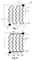
- FIGS. 1 to 4 There are shown four different embodiments of membrane arrangements 10a-10d , each consisting of a conductor track 20a-20d .
- the membrane arrangements each comprise a silicon chip 14 of 5 ⁇ 5 mm made of monocrystalline silicon with a membrane thickness of 1 ⁇ m.
- the dashed rectangles define the actual membrane region 16 , in which a number of holes 18 are arranged.
- the holes in each of these preferred embodiments have a diameter of about 450 nm. Smaller or significantly larger holes may be provided.
- a trace 20a extends substantially over the entire area of the Diaphragm portion 16 and although a meandering or wave 18 to match the holes on both ends of the strip conductor 20a are provided contacts 22, via which a detector means not shown, is connected to the conductor line 20a.
- This detector device preferably measures the electrical resistance of the conductor track 20a. In the event of cracking, the crack will eventually reach the conductor track 20a and sever it. Thus, the electrical resistance of the conductor 20a increases , which can be detected by the detector device. This can, for example, generate a warning signal or put the device provided with the membrane out of operation.
- the embodiment according to Fig. 2 is the of Fig. 1 is very similar and differs from the embodiment of FIG. L only in that the conductor 20b runs in narrower loops and thus snuggles against the holes 18 , so that already at onset of cracking, so at an earlier date than in the embodiment according to Fig. L, the membrane state is detected as damaged.
- Fig. 3 shows an embodiment 10c, in which the conductor track 20c is arranged so that the holes 18 are individually completely enclosed, so that a crack formation between adjacent holes 18 inevitably leads to a crack detection. In this case, a relatively complex course of the conductor 20c is required.
- Fig. 4 shows another embodiment 10d, in which the conductor 20d has a significantly greater width than the diameter of the holes 18.
- the conductor 20d can be selected independently of the hole assembly 18 . The production is thus simpler because the conductor 20d does not have to be adapted exactly to the arrangement of the holes 18 .
- the production can preferably take place in that first of all the conductor track 20d is applied to the membrane 16 and only then the holes 18 are produced. Because even if individual holes 18 completely fall into the conductor 20 d , this remains conductive. In this case, the width of the conductor track 20d should be significantly greater than the diameter of the holes 18, preferably at least 150% of the hole diameter, so that in the production is not accidentally the conductor 20d is already interrupted.
- the conductive line 20d will preferably be arranged in tight loops, so that the uncovered areas with holes are as small as possible.
- Fig. 5 essentially corresponds to that of Fig. L with the difference that a plurality of circuitally parallel tracks 20 e are provided which lead to buses 24 a, 24 b , which are connected to the contacts 22 .
- the individual interconnects 20e must have a predetermined line resistance, because only the change in the total resistance can be measured as an error. Therefore, it is useful if not too many parallel tracks 20e are provided (preferably not more than about 5), because then the detection of an interruption is metrologically problematic, because the resistance then changes only slightly (parallel connection of resistors), if one of parallel tracks 20e is interrupted.
- Fig. 6 1 shows an embodiment 10f in which the holes 18 are surrounded by two conductor tracks 20f, 20g , wherein these two conductor tracks 20f, 20g extend transversely, preferably perpendicular, to one another and thus in particular enclose each hole 18 individually.
- the two tracks 20f, 20g can, as in Fig. 6 shown, be connected separately or electrically connected in series or in parallel.
- the two conductor tracks 20f, 20g can on different sides of the Membrane 14 may be attached or on the same side and separated from each other by means of a thin electrically non-conductive intermediate layer.
- FIG. 10 shows an embodiment 10i in which n-type or p-type doped semiconductors are formed in a membrane made of a semiconductor such as silicon, diamond, SiC, GaN, GaAlN or germanium lanes 20i and 20j , which are conductive therewith and, as in FIG Fig. 7 shown - may be contacted individually or may be connected to each other similar to the embodiments according to the previous drawings.
- the conductor tracks 20i, 20j wider than the hole diameter, which simplifies the production.
- the tracks can be made thinner and similar to the Fig. 1 . 2 . 3 . 5 or 6 be arranged.
- n- and / or p-conductive regions can be generated, which are isolated from one another by blocking pn junctions because of space charge zones.
- n- and / or p-conductive regions can be generated, which are isolated from one another by blocking pn junctions because of space charge zones.
- the conductivity of the tracks 20i, 20j can be varied by suitable doping. As a result, the sensitivity of the crack detection can be adjusted.
- the invention is particularly suitable for applications for biosensing or cleaning of fluids, without this being limiting.
- the invention can be applied to very large-area structures, since suitable production methods such as laser structuring are available for this purpose.
Landscapes
- Chemical & Material Sciences (AREA)
- Chemical Kinetics & Catalysis (AREA)
- Physics & Mathematics (AREA)
- General Physics & Mathematics (AREA)
- Engineering & Computer Science (AREA)
- Manufacturing & Machinery (AREA)
- Investigating Or Analyzing Materials By The Use Of Electric Means (AREA)
Abstract
Description
- Die Erfindung betrifft eine Membran. Die Anwendung von undurchlässigen oder teildurchlässigen Membranen in der Technik sind vielfältig. Insbesondere teildurchlässige Membrane weisen häufig Löcher oder Durchbrüche mit einem bestimmten Durchmesser auf, um Stoffe mit geringerem Partikeldurchmesser passieren zu lassen aber Stoffe mit größerem Partikeldurchmesser zurückzuhalten. Derartige Membrane unterliegen vor allem an den Löchern einem Verschleiß, d.h. es bilden sich Risse, die von einem Loch ausgehend durch die Membran wachsen. Insbesondere bei mikromechanischen Membranen mit Löchern von geringem Durchmesser im Bereich 1 µm und kleiner ist die Erfassung des Zustands der Membran, insbesondere ob diese Risse aufweist, sehr schwierig. Membrane mit Rissen lassen dann unerwünschterweise auch solche Partikel passieren, die eigentlich zurückgehalten werden sollten. Gerade bei Anwendungen im medizinischen oder hygienischen Bereich kann es dann zur Beeinträchtigung der Funktion kommen. Beispielsweise bei einem Wasserfilter, der Bakterien mit einem Partikeldurchmesser von ca. 1 µm durch einen Lochdurchmesser von 450 nm zurückhalten sollte, würden diese bei einem Riss zwischen benachbarten Löchern passieren können. Aufgrund der geringen Strukturgröße ist es schwierig, derartige mikroskopische Risse festzustellen.
- Aufgabe der Erfindung ist es daher, eine Membran bereitzustellen, deren Zustand feststellbar ist. Es sollen also insbesondere Risse oder andere funktionsbeeinträchtigende Schadstellen zuverlässig feststellbar sein.
- Erfindungsgemäß wird diese Aufgabe durch die im Anspruch l angegebenen Merkmale gelöst. Vorteilhafte Weiterbildungen ergeben sich aus den Unteransprüchen.
- Die Erfindung ermöglicht die Überwachung des Zustandes der Membran (also ob diese funktionsfähig bzw. intakt ist) durch Erfassung des elektrischen Stromes durch die mindestens eine Leiterbahn. Dazu ist die mindestens eine Membran zumindest an den besonders rissgefährdeten Bereichen oder aber über der gesamten Membranfläche mit einer oder mehreren Leiterbahnen bedeckt. Diese Leiterbahnen sind dazu sehr dünn und empfindlich gestaltet, damit diese sofort unterbrochen werden, wenn diese vom Riss erreicht werden.
- Wenn sich ein Riss gebildet hat, wird dieser also ab einer gewissen Größe bzw. Erstreckung die Leiterbahn erreichen und durchtrennen. Damit fließt kein oder fast kein Strom mehr und eine Fehlermeldung kann ausgegeben werden. Der Zustand der Membran kann auch über ein Detektionssystem gemäß der
DE 10 2004 030 380 A1 überwacht werden. - Vorzugsweise wird eine einzige Leiterbahn vorgesehen sein, welche mäander- oder schleifenartig die Membranoberfläche zumindest teilweise oder aber komplett bedeckt. Es kann eine gleichmäßige Beabstandung der einzelnen Leiterbahnschleifen vorgesehen werden oder eine engere Führung an gefährdeten Stellen. Es können auch mehrere elektrisch parallelgeschaltete Leiterbahnen vorgesehen sein. Außerhalb des Membranbereichs sind Kontakte vorgesehen, die mit der Leiterbahn kommunizieren und über die ein Detektionssystem mit der Leiterbahn elektrisch kontaktiert ist. Hierzu eignen sich insbesondere gefederte Kontaktstifte welche durch einen Dichtring, der über die Leiterbahn verläuft, vor dem flüssigen Medium geschützt sind.
- Vorzugsweise hat die mindestens eine Leiterbahn eine Dicke von 10 - 1000 nm, vorzugsweise 20 - 100 nm. Damit ist sichergestellt, dass die Leiterbahn einer Rissfortbildung keinen wesentlichen Widerstand entgegensetzt, welche sonst zu einer Rissfortbildung entlang der (parallel zur) Leiterbahn führen könnte, wodurch ein Riss wachsen könnte, ohne dass dies erfasst wird.
- Vorzugsweise hat die mindestens eine Leiterbahn eine Breite von 50 nm - 100 µm, vorzugsweise 100 nm - 500 nm. Damit ist eine Anordnung der Leiterbahn zwischen den häufig eng angeordneten Löchern in einer Membran möglich.
- Vorzugsweise ist die mindestens eine Leiterbahn mit einer Passivierungsschicht versehen, vorzugsweise aus SiO2, Si3N4, Diamant bzw. Diamant-ähnlichen Schichten, Polymeren wie Polycarbonat oder SiC. Damit ist sichergestellt, dass diese nicht vom Medium angegriffen wird, das die Membran umströmt, wodurch Fehlanzeigen vermieden werden.
- Eine bevorzugte Weiterbildung der Erfindung sieht vor, dass auf beiden Seiten der Membran mindestens eine Leiterbahn angeordnet ist. Dies ermöglicht entweder eine großzügigere Anordnung jeder der beiden Leiterbahnen ohne eine Beeinträchtigung der Überwachungsfunktion. Es ist dabei zweckmäßig, wenn die Leiterbahnen auf beiden Seiten mehr oder wenig quer zueinander verlaufen und auf diese Weise beispielsweise über zwei einfach zu fertigende Leiterbahnreihen, die jeweils aus parallelen Leiterbahnabschnitten bestehen, aber die Leiterbahnabschnitte beider Seiten senkrecht zueinander stehen, läßt sich ein engmaschiges Leiterbahnnetz bilden. Dies ist insbesondere von Vorteil, wenn regelmäßig angeordnete Löcher eng zu umschließen sind.
- Alternativ kann eine Membran mit einer Anzahl Löcher auch mit einer Leiterbahn versehen sein, die sich schlangenlinien- oder wellenartig um die Löcher schmiegt.
- Eine alternative Ausbildung sieht vor, dass bei einer Membran mit Löchern die Leiterbahn eine größere Breite aufweist als die Löcher. Die Fertigung einer solchen Membran wird am zweckmäßigsten dadurch erfolgen, dass zunächst die mindestens eine Leiterbahn auf der Membran vorgesehen wird und anschließend die Löcher ausgebildet werden. Dann kann die Löcheranordnung relativ willkürlich zum Verlauf der Leiterbahn erfolgen, da selbst die Anordnung von Löchern direkt in den Leiterbahnbereichen nicht zu einer Unterbrechung derselben führt. Alternativ können zuerst die Löcher und erst dann die Leiterbahn ausgebildet werden. Insbesondere bei kleinen Lochdurchmessern ist deren störender Einfluss auf weitere Herstellungsprozesse noch geringer und es ist möglich, auch noch nach der Ausbildung der Löcher die Leiterbahn aufzubringen und fotolithografisch oder anderweitig zu strukturieren.
- Noch eine bevorzugte Weiterbildung der Erfindung sieht vor, dass die Membran aus einem Material besteht, das durch gezielte n- und/oder p-Dotierung (Grunddotierung) leitfähig machbar ist und die mindestens eine Leiterbahn als gezielte Dotierung (im Gegensatz zur Grunddotierung) der Membran an den Stellen gebildet ist, wo die mindestens eine Leiterbahn verlaufen soll. Geeignete Materialien sind insbesondere Halbleiter wie Silizium, Germanium, GaN, GaAlN, Diamant bzw. Diamant-ähnliche Schichten oder SiC.
- Für die Herstellung einer erfindungsgemäßen Membran sind mehrere Verfahren möglich. Die drei notwendigen Schritte: (a) Membran herstellen, (b) Löcher fertigen, (c) Leiterbahnen aufbringen können in jeder beliebigen Reihenfolge nacheinander erfolgen aber besonders bevorzugt ist die Reihenfolge (c) (b) (a).
- Die Erfindung wird anhand der beigefügten Zeichnungen weiter erläutert. Dabei zeigt:
- Fig. 1:
- eine erste Ausführung einer Membran mit einer Leiterbahn;
- Fig. 2:
- eine zweite Ausführung einer Membran mit einer Leiterbahn;
- Fig. 3:
- einen Ausschnitt einer dritten Ausführung einer Membran mit einer Leiterbahn;
- Fig. 4:
- eine vierte Ausführung einer Membran mit einer Leiterbahn;
- Fig. 5:
- eine Ausführung einer Membran mit mehreren parallel geschalteten Leiterbahnen;
- Fig. 6:
- eine Ausführung mit zwei quer zueinander laufenden Leiterbahnen;
- Fig. 7:
- eine Ausführung mit einer durch Dotierung gebildeten Leiterbahn.
- In den
Figuren 1 bis 4 sind vier verschiedene Ausführungen von Membrananordnungen 10a - 10d dargestellt, die jeweils aus einer Leiterbahn 20a - 20d bestehen. Die Membrananordnungen umfassen bei diesen Ausführungsbeispielen jeweils einen Siliziumchip 14 von 5 x 5 mm aus einkristallinem Silizium mit einer Membrandicke von 1 µm. Durch die gestrichelten Rechtecke wird der eigentliche Membranbereich 16 definiert, in dem eine Anzahl Löcher 18 angeordnet sind. Die Löcher haben bei diesen bevorzugten Ausführungsbeispielen jeweils einen Durchmesser von etwa 450 nm. Es können auch kleinere oder deutlich größere Löcher vorgesehen werden. - Bei der Ausführung gemäß
Fig. 1 erstreckt sich eine Leiterbahn 20a im wesentlichen über die gesamte Fläche des Membranbereichs 16 und zwar mäander- oder wellenartig in Anpassung an die Löcher 18. Beidendig an der Leiterbahn 20a sind Kontakte 22 vorgesehen, über die eine nicht gezeigte Detektoreinrichtung an die Leiterbahn 20a anschließbar ist. Vorzugsweise misst diese Detektoreinrichtung den elektrischen Widerstand der Leiterbahn 20a. Bei einer Rissbildung wird der Riss irgendwann die Leiterbahn 20a erreichen und diese durchtrennen. Damit steigt der elektrische Widerstand der Leiterbahn 20a an, was von der Detektoreinrichtung feststellbar ist. Diese kann beispielsweise ein Warnsignal erzeugen oder auch die mit der Membran versehene Vorrichtung außer Betrieb setzen. - Die Ausführungsform gemäß
Fig. 2 ist der vonFig. 1 sehr ähnlich und unterscheidet sich von der Ausführungsform gemäß Fig. l nur dadurch, dass die Leiterbahn 20b in engeren Schleifen verläuft und sich damit enger an die Löcher 18 anschmiegt, so dass bereits bei einsetzender Rissbildung, also zu einem früheren Zeitpunkt als bei der Ausführung gemäß Fig. l, der Membranzustand als beschädigt feststellbar ist. -
Fig. 3 zeigt eine Ausführung 10c, bei der die Leiterbahn 20c so angeordnet ist, dass die Löcher 18 einzeln vollständig umschlossen werden, so dass eine Rissausbildung zwischen benachbarten Löchern 18 zwangsläufig zu einer Rissdetektion führt. Dabei ist ein relativ komplexer Verlauf der Leiterbahn 20c erforderlich. -
Fig. 4 zeigt eine andere Ausführung 10d, bei der die Leiterbahn 20d eine deutlich größere Breite aufweist als die Durchmesser der Löcher 18. Bei dieser Ausführung kann die Leiterbahn 20d unabhängig von der Löcheranordnung 18 gewählt werden. Die Herstellung ist also einfacher, weil die Leiterbahn 20d nicht genau an die Anordnung der Löcher 18 angepasst werden muss. - Die Herstellung kann vorzugsweise dadurch erfolgen, dass zunächst die Leiterbahn 20d auf der Membran 16 aufgebracht wird und erst anschließend die Löcher 18 gefertigt werden. Denn selbst wenn einzelne Löcher 18 vollständig in die Leiterbahn 20d fallen, bleibt diese leitfähig. Dabei sollte die Breite der Leiterbahn 20d signifikant größer sein als der Durchmesser der Löcher 18, vorzugsweise mindestens 150% des Lochdurchmessers, damit bei der Fertigung nicht aus Versehen die Leiterbahn 20d bereits unterbrochen wird. Die Leiterbahn 20d wird vorzugsweise in engen Schleifen angeordnet sein, damit die nicht überdeckten Bereiche mit Löchern so klein wie möglich sind.
- Die Ausführung gemäß
Fig. 5 entspricht im wesentlichen der von Fig. l mit dem Unterschied, dass mehrere schaltungstechnisch parallele Leiterbahnen 20e vorgesehen sind, die zu Sammelleitungen 24a, 24b führen, die mit den Kontakten 22 verbunden sind. Bei dieser Variante müssen die einzelnen Leiterbahnen 20e einen vorgegebenen Leitungswiderstand aufweisen, denn als Fehler messbar ist nur die Änderung des Gesamtwiderstandes. Daher ist es zweckmäßig, wenn nicht zu viele parallele Leiterbahnen 20e vorgesehen werden (vorzugsweise nicht mehr als etwa 5), weil dann die Erfassung einer Unterbrechung messtechnisch problematischer wird, denn der Widerstand ändert sich dann nur unwesentlich (Parallelschaltung von Widerständen), wenn eine der parallelen Leiterbahnen 20e unterbrochen ist. -
Fig. 6 zeigt eine Ausführungsform 10f, bei der die Löcher 18 von zwei Leiterbahnen 20f, 20g umgeben sind, wobei diese beiden Leiterbahnen 20f, 20g quer, vorzugsweise senkrecht, zueinander verlaufen und damit insbesondere jedes Loch 18 einzeln umschließen. Die beiden Leiterbahnen 20f, 20g können, wie inFig. 6 dargestellt, separat beschaltet werden oder aber elektrisch in Reihe oder parallel geschaltet sein. Die beiden Leiterbahnen 20f, 20g können auf unterschiedlichen Seiten der Membran 14 angebracht sein oder aber auf der gleichen Seite und mittels einer dünnen elektrisch nichtleitenden Zwischenschicht voneinander getrennt sein. -
Fig. 7 zeigt eine Ausführungsform 10i, bei der in eine Membran aus einem Halbleiter wie Silizium, Diamant, SiC, GaN, GaAlN oder Germanium Bahnen 20i und 20j n- oder p-dotierter Halbleiter gebildet werden, die damit leitfähig sind und - wie inFig. 7 gezeigt - einzeln kontaktiert sein oder aber ähnlich den Ausführungen gemäß der vorherigen Zeichnungen miteinander verbunden sein können. Bei der inFig. 7 gezeigten Ausführung sind ähnlich wie beiFig. 4 , die Leiterbahnen 20i, 20j breiter als die Lochdurchmesser, was die Herstellung vereinfacht. Alternativ können die Leiterbahnen auch dünner ausgeführt und ähnlich derFig. 1 ,2 ,3 ,5 oder6 angeordnet sein. Damit können n- und/oder p-leitfähige Bereiche erzeugt werden, die aufgrund von Raumladungszonen durch sperrende pn-Übergänge voneinander isoliert sind. Abhängig von der Breite der Leiterbahnen 20i, 20j kommt es entweder zu einem kompletten Verlust der Leitfähigkeit oder zu einem signifikanten Anstieg des Widerstandes. Die Leitfähigkeit der Leiterbahnen 20i, 20j kann durch geeignetes Dotieren variiert werden. Hierdurch kann die Sensitivität der Rissdetektion angepasst werden. - Außerdem stellt die Erfindung die folgenden Ausführungsformen bereit:
- Ausführungsform 1: Membran, dadurch gekennzeichnet, dass diese mit mindestens einer stromdurchflossenen Leiterbahn (20) versehen ist, die bei Beschädigung der Membran unterbrechbar ist und der Zustand der Membran durch Erfassung des elektrischen Stromes durch die Leiterbahn bestimmbar ist.
- Ausführungsform 2: Membran nach Ausführungsform 1, dadurch gekennzeichnet, dass die mindestens eine Leiterbahn (20) schleifenartig auf der Membran (14) angeordnet ist und diese im Wesentlichen abdeckt.
- Ausführungsform 3: Membran nach Ausführungsform 1, dadurch gekennzeichnet, dass die mindestens eine Leiterbahn eine Dicke von 10 nm - 100 µm, vorzugsweise 20 nm - 500 nm aufweist.
- Ausführungsform 4: Membran nach Ausführungsform 1, dadurch gekennzeichnet, dass die mindestens eine Leiterbahn eine Breite von 50 nm - 100 µm, vorzugsweise 100 nm - 500 nm aufweist.
- Ausführungsform 5: Membran nach Ausführungsform 1, dadurch gekennzeichnet, dass die mindestens eine Leiterbahn mit einer Passivierungsschicht versehen ist.
- Ausführungsform 6: Membran nach einer der vorherigen Ausführungsformen, dadurch gekennzeichnet, dass die mindestens eine Leiterbahn mäanderartig angeordnet ist.
- Ausführungsform 7: Membran nach einer der vorherigen Ausführungsformen, durch gekennzeichnet, dass auf beiden Seiten der Membran mindestens eine Leiterbahn angeordnet ist.
- Ausführungsform 8: Membran nach einer der vorherigen Ausführungsformen, dadurch gekennzeichnet, dass diese eine Anzahl Löcher aufweist und die mindestens eine Leiterbahn die Löcher zumindest weitgehend umschließt.
- Ausführungsform 9: Membran nach Ausführungsform 7, dadurch gekennzeichnet, dass die mindestens eine Leiterbahn schlangenlinienartig zwischen den Löchern verläuft.
- Ausführungsform 10: Membran nach einer der Ausführungsformen 1 bis 6, dadurch gekennzeichnet, dass diese eine Anzahl Löcher aufweist und die mindestens eine Leiterbahn eine größere Breite aufweist als die Löcher.
- Ausführungsform 11: Membran nach Ausführungsform 1, dadurch gekennzeichnet, dass die Membran aus einem Material besteht, das durch gezielte n- oder p-Dotierung leitfähig machbar ist und die mindestens eine Leiterbahn als bereichsweise Dotierung der Membran gebildet ist.
- Ausführungsform 12: Membran nach Ausführungsform 11, dadurch gekennzeichnet, dass die Membran aus Silizium, Germanium, GaN, GaAlN, Diamant, Diamant-ähnlichem Material oder SiC besteht.
- Die Erfindung eignet sich insbesondere für Anwendungen zur Biosensorik oder Reinigung von Fluiden, ohne dass dies beschränkend wäre. Die Erfindung läßt sich auf sehr großflächige Strukturen anwenden, da hierfür geeignete Herstellungsverfahren wie Laserstrukturierung zur Verfügung stehen.
Claims (11)
- Membran, dadurch gekennzeichnet, dass diese mit mindestens einer stromdurchflossenen Leiterbahn (20) versehen ist, die bei Beschädigung der Membran unterbrechbar ist und der Zustand der Membran durch Erfassung des elektrischen Stromes durch die Leiterbahn bestimmbar ist, wobei auf beiden Seiten der Membran mindestens eine Leiterbahn angeordnet ist.
- Membran nach Anspruch 1, dadurch gekennzeichnet, dass die mindestens eine Leiterbahn (20) schleifenartig auf der Membran (14) angeordnet ist und diese im Wesentlichen abdeckt.
- Membran nach Anspruch 1, dadurch gekennzeichnet, dass die mindestens eine Leiterbahn eine Dicke von 10 nm - 100 µm, vorzugsweise 20 nm - 500 nm aufweist.
- Membran nach Anspruch 1, dadurch gekennzeichnet, dass die mindestens eine Leiterbahn eine Breite von 50 nm - 100 µm, vorzugsweise 100 nm - 500 nm aufweist.
- Membran nach Anspruch 1, dadurch gekennzeichnet, dass die mindestens eine Leiterbahn mit einer Passivierungsschicht versehen ist.
- Membran nach einem der vorherigen Ansprüche, dadurch gekennzeichnet, dass die mindestens eine Leiterbahn mäanderartig angeordnet ist.
- Membran nach einem der vorherigen Ansprüche, dadurch gekennzeichnet, dass diese eine Anzahl Löcher aufweist und die mindestens eine Leiterbahn die Löcher zumindest weitgehend umschließt.
- Membran nach einem der vorherigen Ansprüche, dadurch gekennzeichnet, dass die mindestens eine Leiterbahn schlangenlinienartig zwischen den Löchern verläuft.
- Membran nach einem der Ansprüche 1 bis 6, dadurch gekennzeichnet, dass diese eine Anzahl Löcher aufweist und die mindestens eine Leiterbahn eine größere Breite aufweist als die Löcher.
- Membran nach Anspruch 1, dadurch gekennzeichnet, dass die Membran aus einem Material besteht, das durch gezielte n- oder p-Dotierung leitfähig machbar ist und die mindestens eine Leiterbahn als bereichsweise Dotierung der Membran gebildet ist.
- Membran nach Anspruch 10, dadurch gekennzeichnet, dass die Membran aus Silizium, Germanium, GaN, GaAlN, Diamant, Diamant-ähnlichem Material oder SiC besteht.
Applications Claiming Priority (3)
| Application Number | Priority Date | Filing Date | Title |
|---|---|---|---|
| DE102009022913A DE102009022913A1 (de) | 2009-05-27 | 2009-05-27 | Membran mit Mitteln zur Zustandüberwachung |
| EP10722305.9A EP2435169B1 (de) | 2009-05-27 | 2010-05-19 | Membran mit mitteln zur zustandüberwachung |
| PCT/EP2010/003072 WO2010136148A1 (de) | 2009-05-27 | 2010-05-19 | Membran mit mitteln zur zustandüberwachung |
Related Parent Applications (1)
| Application Number | Title | Priority Date | Filing Date |
|---|---|---|---|
| EP10722305.9A Division EP2435169B1 (de) | 2009-05-27 | 2010-05-19 | Membran mit mitteln zur zustandüberwachung |
Publications (2)
| Publication Number | Publication Date |
|---|---|
| EP2796186A1 true EP2796186A1 (de) | 2014-10-29 |
| EP2796186B1 EP2796186B1 (de) | 2019-08-07 |
Family
ID=42676698
Family Applications (2)
| Application Number | Title | Priority Date | Filing Date |
|---|---|---|---|
| EP10722305.9A Not-in-force EP2435169B1 (de) | 2009-05-27 | 2010-05-19 | Membran mit mitteln zur zustandüberwachung |
| EP14176215.3A Active EP2796186B1 (de) | 2009-05-27 | 2010-05-19 | Membran mit Mitteln zur Zustandüberwachung |
Family Applications Before (1)
| Application Number | Title | Priority Date | Filing Date |
|---|---|---|---|
| EP10722305.9A Not-in-force EP2435169B1 (de) | 2009-05-27 | 2010-05-19 | Membran mit mitteln zur zustandüberwachung |
Country Status (5)
| Country | Link |
|---|---|
| US (1) | US8872187B2 (de) |
| EP (2) | EP2435169B1 (de) |
| CN (1) | CN102448590B (de) |
| DE (1) | DE102009022913A1 (de) |
| WO (1) | WO2010136148A1 (de) |
Cited By (1)
| Publication number | Priority date | Publication date | Assignee | Title |
|---|---|---|---|---|
| RU2752797C1 (ru) * | 2020-10-08 | 2021-08-06 | федеральное государственное автономное образовательное учреждение высшего образования "Московский физико-технический институт (национальный исследовательский университет)" | Устройство для исследования структурных и транспортных свойств мембран в условиях контролируемой температуры и влажности окружающей среды |
Families Citing this family (2)
| Publication number | Priority date | Publication date | Assignee | Title |
|---|---|---|---|---|
| DE102009022913A1 (de) | 2009-05-27 | 2010-12-09 | Eads Deutschland Gmbh | Membran mit Mitteln zur Zustandüberwachung |
| US10067007B2 (en) * | 2015-09-02 | 2018-09-04 | Oculus Vr, Llc | Resistive-capacitive deformation sensor |
Citations (6)
| Publication number | Priority date | Publication date | Assignee | Title |
|---|---|---|---|---|
| DE19926372A1 (de) * | 1999-06-10 | 2001-02-01 | Freudenberg Carl Fa | Einrichtung zur Erkennung von Undichtheiten an Membranen |
| US6541676B1 (en) * | 1998-12-02 | 2003-04-01 | Massachusetts Institute Of Technology | Integrated palladium-based micromembranes for hydrogen separation and hydrogenation/dehydrogenation reactions |
| EP1441209A2 (de) * | 2003-01-24 | 2004-07-28 | VARIAN S.p.A. | Gasselektive permeabele Membrane und Herstellungsverfahren dafür |
| WO2005105276A2 (en) * | 2004-05-03 | 2005-11-10 | Friesland Brands B.V. | Device with a membrane on a carrier, as well as a method for manufacturing such a membrane |
| DE102004030380A1 (de) | 2004-06-23 | 2006-01-19 | Eads Deutschland Gmbh | Mikromechanische Membran- oder Brückenstruktur, insbesondere mikromechanischer Sensor oder Aktor, und Verfahren zum Selbsttest einer solchen |
| WO2009033226A1 (en) * | 2007-09-14 | 2009-03-19 | Inphaze Pty Ltd | In situ membrane monitoring |
Family Cites Families (6)
| Publication number | Priority date | Publication date | Assignee | Title |
|---|---|---|---|---|
| US3278881A (en) * | 1961-07-25 | 1966-10-11 | Gen Electric | Membrane strain gauge |
| US6635910B1 (en) | 1999-07-22 | 2003-10-21 | Measurement Specialties, Inc. | Silicon strain gage having a thin layer of highly conductive silicon |
| US7104113B2 (en) | 2003-11-21 | 2006-09-12 | General Electric Company | Miniaturized multi-gas and vapor sensor devices and associated methods of fabrication |
| NL1026097C2 (nl) * | 2004-05-03 | 2005-11-07 | Cornelis Johannes Maria V Rijn | Membraan, alsmede werkwijze ter vervaardiging van een dergelijk membraan. |
| DE102005001098A1 (de) | 2005-01-08 | 2006-07-20 | Abb Patent Gmbh | Drucksensor (II) |
| DE102009022913A1 (de) | 2009-05-27 | 2010-12-09 | Eads Deutschland Gmbh | Membran mit Mitteln zur Zustandüberwachung |
-
2009
- 2009-05-27 DE DE102009022913A patent/DE102009022913A1/de not_active Ceased
-
2010
- 2010-05-19 EP EP10722305.9A patent/EP2435169B1/de not_active Not-in-force
- 2010-05-19 CN CN201080023433.9A patent/CN102448590B/zh not_active Expired - Fee Related
- 2010-05-19 WO PCT/EP2010/003072 patent/WO2010136148A1/de not_active Ceased
- 2010-05-19 EP EP14176215.3A patent/EP2796186B1/de active Active
-
2011
- 2011-11-22 US US13/302,629 patent/US8872187B2/en not_active Expired - Fee Related
Patent Citations (6)
| Publication number | Priority date | Publication date | Assignee | Title |
|---|---|---|---|---|
| US6541676B1 (en) * | 1998-12-02 | 2003-04-01 | Massachusetts Institute Of Technology | Integrated palladium-based micromembranes for hydrogen separation and hydrogenation/dehydrogenation reactions |
| DE19926372A1 (de) * | 1999-06-10 | 2001-02-01 | Freudenberg Carl Fa | Einrichtung zur Erkennung von Undichtheiten an Membranen |
| EP1441209A2 (de) * | 2003-01-24 | 2004-07-28 | VARIAN S.p.A. | Gasselektive permeabele Membrane und Herstellungsverfahren dafür |
| WO2005105276A2 (en) * | 2004-05-03 | 2005-11-10 | Friesland Brands B.V. | Device with a membrane on a carrier, as well as a method for manufacturing such a membrane |
| DE102004030380A1 (de) | 2004-06-23 | 2006-01-19 | Eads Deutschland Gmbh | Mikromechanische Membran- oder Brückenstruktur, insbesondere mikromechanischer Sensor oder Aktor, und Verfahren zum Selbsttest einer solchen |
| WO2009033226A1 (en) * | 2007-09-14 | 2009-03-19 | Inphaze Pty Ltd | In situ membrane monitoring |
Cited By (1)
| Publication number | Priority date | Publication date | Assignee | Title |
|---|---|---|---|---|
| RU2752797C1 (ru) * | 2020-10-08 | 2021-08-06 | федеральное государственное автономное образовательное учреждение высшего образования "Московский физико-технический институт (национальный исследовательский университет)" | Устройство для исследования структурных и транспортных свойств мембран в условиях контролируемой температуры и влажности окружающей среды |
Also Published As
| Publication number | Publication date |
|---|---|
| EP2796186B1 (de) | 2019-08-07 |
| EP2435169B1 (de) | 2014-07-09 |
| US20120126248A1 (en) | 2012-05-24 |
| CN102448590A (zh) | 2012-05-09 |
| WO2010136148A1 (de) | 2010-12-02 |
| DE102009022913A1 (de) | 2010-12-09 |
| CN102448590B (zh) | 2015-04-08 |
| EP2435169A1 (de) | 2012-04-04 |
| US8872187B2 (en) | 2014-10-28 |
Similar Documents
| Publication | Publication Date | Title |
|---|---|---|
| DE102018201997B4 (de) | Emitterstruktur und Herstellungsverfahren | |
| DE10238265B4 (de) | Halbleiterbauelement und Verfahren zu dessen Herstellung | |
| DE2926741C2 (de) | Feldeffekt-Transistor und Verfahren zu seiner Herstellung | |
| DE69513749T2 (de) | Thermischer Mikrodurchflusssensor und sein Herstellungsverfahren | |
| EP2796186B1 (de) | Membran mit Mitteln zur Zustandüberwachung | |
| EP2901134A1 (de) | Sensor zur detektion von teilchen | |
| DE102004008008B4 (de) | Integrierter Flusssensor zum Messen eines Fluidflusses und Verfahren zum Herstellen eines Flusssensors | |
| EP2171437A1 (de) | Sensorelement zur detektion von leitfähigen partikeln in einem gasstrom sowie verfahren zu dessen herstellung und dessen verwendung | |
| DE102012202035B4 (de) | Mikromechanisches Bauelement mit einer Membran | |
| DE102008041750A1 (de) | Thermisch entkoppeltes mikrostrukturiertes Referenzelement für Sensoren | |
| EP3430364B1 (de) | Faserverstärkter verbundwerkstoff mit einer sensoranordnung zur strukturüberwachung des verbundwerkstoffs | |
| WO2015022028A1 (de) | Partikelsensor und verfahren zum herstellen eines partikelsensors | |
| DE102008007222A1 (de) | Halbleitervorrichtung mit Störstellen dotiertem Widerstandselement | |
| DE102007008381A1 (de) | Strahlungssensorelement, Verfahren zur Herstellung eines Strahlungssensorelements und Sensorfeld | |
| DE3874605T2 (de) | Mikrosonde in integrierter schalttechnik zur feststellung bestimmter gase. | |
| DE19511596B4 (de) | Verfahren zum Ätzen von Halbleiterwafern | |
| DE102008041808A1 (de) | Partikelsensor und ein Verfahren zu dessen Herstellung | |
| DE102013217094A1 (de) | Mikromechanisches Bauelement und entsprechendes Prüfverfahren für ein mikromechanisches Bauelement | |
| EP4075469A1 (de) | Mikroelektromechanisches schaltelement, vorrichtung und betriebsverfahren | |
| DE102021132701A1 (de) | Vorrichtung zur steuerung von gefangenen ionen mit einem temperatursensor | |
| DE102006042361A1 (de) | Sensor zur Detektion von Teilchen umfassend eine Prüfvorrichtung zur Überprüfung der Beschaffenheit einer isolierenden Schicht | |
| DE102023212471A1 (de) | Mikroelektromechanischer Gassensor und Verfahren zur Herstellung eines mikroelektromechanischen Gassensors | |
| DE102008021896B4 (de) | Vorrichtung zur Bestimmung einer Messgröße eines Gases | |
| WO2007082950A1 (de) | Bewertung einer unteraetzung von tiefen grabenstrukturen in soi-scheiben | |
| AT528341A1 (de) | Vorrichtung zur Messung von Verunreinigungen in einem Strömungskanal |
Legal Events
| Date | Code | Title | Description |
|---|---|---|---|
| PUAI | Public reference made under article 153(3) epc to a published international application that has entered the european phase |
Free format text: ORIGINAL CODE: 0009012 |
|
| 17P | Request for examination filed |
Effective date: 20140708 |
|
| AC | Divisional application: reference to earlier application |
Ref document number: 2435169 Country of ref document: EP Kind code of ref document: P |
|
| AK | Designated contracting states |
Kind code of ref document: A1 Designated state(s): AL AT BE BG CH CY CZ DE DK EE ES FI FR GB GR HR HU IE IS IT LI LT LU LV MC MK MT NL NO PL PT RO SE SI SK SM TR |
|
| RIN1 | Information on inventor provided before grant (corrected) |
Inventor name: FRIEDBERGER, ALOIS Inventor name: MUELLER, GERHARD Inventor name: HELWIG, ANDREAS |
|
| RIN1 | Information on inventor provided before grant (corrected) |
Inventor name: HELWIG, ANDREAS Inventor name: FRIEDBERGER, ALOIS Inventor name: MUELLER, GERHARD |
|
| R17P | Request for examination filed (corrected) |
Effective date: 20150429 |
|
| RBV | Designated contracting states (corrected) |
Designated state(s): AL AT BE BG CH CY CZ DE DK EE ES FI FR GB GR HR HU IE IS IT LI LT LU LV MC MK MT NL NO PL PT RO SE SI SK SM TR |
|
| STAA | Information on the status of an ep patent application or granted ep patent |
Free format text: STATUS: REQUEST FOR EXAMINATION WAS MADE |
|
| STAA | Information on the status of an ep patent application or granted ep patent |
Free format text: STATUS: EXAMINATION IS IN PROGRESS |
|
| 17Q | First examination report despatched |
Effective date: 20180906 |
|
| GRAP | Despatch of communication of intention to grant a patent |
Free format text: ORIGINAL CODE: EPIDOSNIGR1 |
|
| STAA | Information on the status of an ep patent application or granted ep patent |
Free format text: STATUS: GRANT OF PATENT IS INTENDED |
|
| INTG | Intention to grant announced |
Effective date: 20190226 |
|
| RIN1 | Information on inventor provided before grant (corrected) |
Inventor name: FRIEDBERGER, ALOIS Inventor name: HELWIG, ANDREAS Inventor name: MUELLER, GERHARD |
|
| GRAS | Grant fee paid |
Free format text: ORIGINAL CODE: EPIDOSNIGR3 |
|
| GRAA | (expected) grant |
Free format text: ORIGINAL CODE: 0009210 |
|
| STAA | Information on the status of an ep patent application or granted ep patent |
Free format text: STATUS: THE PATENT HAS BEEN GRANTED |
|
| AC | Divisional application: reference to earlier application |
Ref document number: 2435169 Country of ref document: EP Kind code of ref document: P |
|
| AK | Designated contracting states |
Kind code of ref document: B1 Designated state(s): AL AT BE BG CH CY CZ DE DK EE ES FI FR GB GR HR HU IE IS IT LI LT LU LV MC MK MT NL NO PL PT RO SE SI SK SM TR |
|
| REG | Reference to a national code |
Ref country code: GB Ref legal event code: FG4D Free format text: NOT ENGLISH |
|
| REG | Reference to a national code |
Ref country code: CH Ref legal event code: EP Ref country code: AT Ref legal event code: REF Ref document number: 1162972 Country of ref document: AT Kind code of ref document: T Effective date: 20190815 |
|
| REG | Reference to a national code |
Ref country code: DE Ref legal event code: R096 Ref document number: 502010016180 Country of ref document: DE |
|
| REG | Reference to a national code |
Ref country code: IE Ref legal event code: FG4D Free format text: LANGUAGE OF EP DOCUMENT: GERMAN |
|
| REG | Reference to a national code |
Ref country code: NL Ref legal event code: MP Effective date: 20190807 |
|
| REG | Reference to a national code |
Ref country code: LT Ref legal event code: MG4D |
|
| PG25 | Lapsed in a contracting state [announced via postgrant information from national office to epo] |
Ref country code: FI Free format text: LAPSE BECAUSE OF FAILURE TO SUBMIT A TRANSLATION OF THE DESCRIPTION OR TO PAY THE FEE WITHIN THE PRESCRIBED TIME-LIMIT Effective date: 20190807 Ref country code: LT Free format text: LAPSE BECAUSE OF FAILURE TO SUBMIT A TRANSLATION OF THE DESCRIPTION OR TO PAY THE FEE WITHIN THE PRESCRIBED TIME-LIMIT Effective date: 20190807 Ref country code: PT Free format text: LAPSE BECAUSE OF FAILURE TO SUBMIT A TRANSLATION OF THE DESCRIPTION OR TO PAY THE FEE WITHIN THE PRESCRIBED TIME-LIMIT Effective date: 20191209 Ref country code: HR Free format text: LAPSE BECAUSE OF FAILURE TO SUBMIT A TRANSLATION OF THE DESCRIPTION OR TO PAY THE FEE WITHIN THE PRESCRIBED TIME-LIMIT Effective date: 20190807 Ref country code: NL Free format text: LAPSE BECAUSE OF FAILURE TO SUBMIT A TRANSLATION OF THE DESCRIPTION OR TO PAY THE FEE WITHIN THE PRESCRIBED TIME-LIMIT Effective date: 20190807 Ref country code: SE Free format text: LAPSE BECAUSE OF FAILURE TO SUBMIT A TRANSLATION OF THE DESCRIPTION OR TO PAY THE FEE WITHIN THE PRESCRIBED TIME-LIMIT Effective date: 20190807 Ref country code: BG Free format text: LAPSE BECAUSE OF FAILURE TO SUBMIT A TRANSLATION OF THE DESCRIPTION OR TO PAY THE FEE WITHIN THE PRESCRIBED TIME-LIMIT Effective date: 20191107 Ref country code: NO Free format text: LAPSE BECAUSE OF FAILURE TO SUBMIT A TRANSLATION OF THE DESCRIPTION OR TO PAY THE FEE WITHIN THE PRESCRIBED TIME-LIMIT Effective date: 20191107 |
|
| PG25 | Lapsed in a contracting state [announced via postgrant information from national office to epo] |
Ref country code: ES Free format text: LAPSE BECAUSE OF FAILURE TO SUBMIT A TRANSLATION OF THE DESCRIPTION OR TO PAY THE FEE WITHIN THE PRESCRIBED TIME-LIMIT Effective date: 20190807 Ref country code: GR Free format text: LAPSE BECAUSE OF FAILURE TO SUBMIT A TRANSLATION OF THE DESCRIPTION OR TO PAY THE FEE WITHIN THE PRESCRIBED TIME-LIMIT Effective date: 20191108 Ref country code: LV Free format text: LAPSE BECAUSE OF FAILURE TO SUBMIT A TRANSLATION OF THE DESCRIPTION OR TO PAY THE FEE WITHIN THE PRESCRIBED TIME-LIMIT Effective date: 20190807 Ref country code: IS Free format text: LAPSE BECAUSE OF FAILURE TO SUBMIT A TRANSLATION OF THE DESCRIPTION OR TO PAY THE FEE WITHIN THE PRESCRIBED TIME-LIMIT Effective date: 20191207 Ref country code: AL Free format text: LAPSE BECAUSE OF FAILURE TO SUBMIT A TRANSLATION OF THE DESCRIPTION OR TO PAY THE FEE WITHIN THE PRESCRIBED TIME-LIMIT Effective date: 20190807 |
|
| PG25 | Lapsed in a contracting state [announced via postgrant information from national office to epo] |
Ref country code: TR Free format text: LAPSE BECAUSE OF FAILURE TO SUBMIT A TRANSLATION OF THE DESCRIPTION OR TO PAY THE FEE WITHIN THE PRESCRIBED TIME-LIMIT Effective date: 20190807 |
|
| PG25 | Lapsed in a contracting state [announced via postgrant information from national office to epo] |
Ref country code: EE Free format text: LAPSE BECAUSE OF FAILURE TO SUBMIT A TRANSLATION OF THE DESCRIPTION OR TO PAY THE FEE WITHIN THE PRESCRIBED TIME-LIMIT Effective date: 20190807 Ref country code: PL Free format text: LAPSE BECAUSE OF FAILURE TO SUBMIT A TRANSLATION OF THE DESCRIPTION OR TO PAY THE FEE WITHIN THE PRESCRIBED TIME-LIMIT Effective date: 20190807 Ref country code: DK Free format text: LAPSE BECAUSE OF FAILURE TO SUBMIT A TRANSLATION OF THE DESCRIPTION OR TO PAY THE FEE WITHIN THE PRESCRIBED TIME-LIMIT Effective date: 20190807 Ref country code: RO Free format text: LAPSE BECAUSE OF FAILURE TO SUBMIT A TRANSLATION OF THE DESCRIPTION OR TO PAY THE FEE WITHIN THE PRESCRIBED TIME-LIMIT Effective date: 20190807 Ref country code: IT Free format text: LAPSE BECAUSE OF FAILURE TO SUBMIT A TRANSLATION OF THE DESCRIPTION OR TO PAY THE FEE WITHIN THE PRESCRIBED TIME-LIMIT Effective date: 20190807 |
|
| PG25 | Lapsed in a contracting state [announced via postgrant information from national office to epo] |
Ref country code: SK Free format text: LAPSE BECAUSE OF FAILURE TO SUBMIT A TRANSLATION OF THE DESCRIPTION OR TO PAY THE FEE WITHIN THE PRESCRIBED TIME-LIMIT Effective date: 20190807 Ref country code: SM Free format text: LAPSE BECAUSE OF FAILURE TO SUBMIT A TRANSLATION OF THE DESCRIPTION OR TO PAY THE FEE WITHIN THE PRESCRIBED TIME-LIMIT Effective date: 20190807 Ref country code: IS Free format text: LAPSE BECAUSE OF FAILURE TO SUBMIT A TRANSLATION OF THE DESCRIPTION OR TO PAY THE FEE WITHIN THE PRESCRIBED TIME-LIMIT Effective date: 20200224 Ref country code: CZ Free format text: LAPSE BECAUSE OF FAILURE TO SUBMIT A TRANSLATION OF THE DESCRIPTION OR TO PAY THE FEE WITHIN THE PRESCRIBED TIME-LIMIT Effective date: 20190807 |
|
| REG | Reference to a national code |
Ref country code: DE Ref legal event code: R097 Ref document number: 502010016180 Country of ref document: DE |
|
| PLBE | No opposition filed within time limit |
Free format text: ORIGINAL CODE: 0009261 |
|
| STAA | Information on the status of an ep patent application or granted ep patent |
Free format text: STATUS: NO OPPOSITION FILED WITHIN TIME LIMIT |
|
| PG2D | Information on lapse in contracting state deleted |
Ref country code: IS |
|
| 26N | No opposition filed |
Effective date: 20200603 |
|
| PG25 | Lapsed in a contracting state [announced via postgrant information from national office to epo] |
Ref country code: SI Free format text: LAPSE BECAUSE OF FAILURE TO SUBMIT A TRANSLATION OF THE DESCRIPTION OR TO PAY THE FEE WITHIN THE PRESCRIBED TIME-LIMIT Effective date: 20190807 |
|
| PG25 | Lapsed in a contracting state [announced via postgrant information from national office to epo] |
Ref country code: LI Free format text: LAPSE BECAUSE OF NON-PAYMENT OF DUE FEES Effective date: 20200531 Ref country code: MC Free format text: LAPSE BECAUSE OF FAILURE TO SUBMIT A TRANSLATION OF THE DESCRIPTION OR TO PAY THE FEE WITHIN THE PRESCRIBED TIME-LIMIT Effective date: 20190807 Ref country code: CH Free format text: LAPSE BECAUSE OF NON-PAYMENT OF DUE FEES Effective date: 20200531 |
|
| REG | Reference to a national code |
Ref country code: BE Ref legal event code: MM Effective date: 20200531 |
|
| GBPC | Gb: european patent ceased through non-payment of renewal fee |
Effective date: 20200519 |
|
| PG25 | Lapsed in a contracting state [announced via postgrant information from national office to epo] |
Ref country code: LU Free format text: LAPSE BECAUSE OF NON-PAYMENT OF DUE FEES Effective date: 20200519 |
|
| PG25 | Lapsed in a contracting state [announced via postgrant information from national office to epo] |
Ref country code: GB Free format text: LAPSE BECAUSE OF NON-PAYMENT OF DUE FEES Effective date: 20200519 Ref country code: IE Free format text: LAPSE BECAUSE OF NON-PAYMENT OF DUE FEES Effective date: 20200519 Ref country code: FR Free format text: LAPSE BECAUSE OF NON-PAYMENT OF DUE FEES Effective date: 20200531 |
|
| PG25 | Lapsed in a contracting state [announced via postgrant information from national office to epo] |
Ref country code: BE Free format text: LAPSE BECAUSE OF NON-PAYMENT OF DUE FEES Effective date: 20200531 |
|
| REG | Reference to a national code |
Ref country code: AT Ref legal event code: MM01 Ref document number: 1162972 Country of ref document: AT Kind code of ref document: T Effective date: 20200519 |
|
| PG25 | Lapsed in a contracting state [announced via postgrant information from national office to epo] |
Ref country code: AT Free format text: LAPSE BECAUSE OF NON-PAYMENT OF DUE FEES Effective date: 20200519 |
|
| PG25 | Lapsed in a contracting state [announced via postgrant information from national office to epo] |
Ref country code: MT Free format text: LAPSE BECAUSE OF FAILURE TO SUBMIT A TRANSLATION OF THE DESCRIPTION OR TO PAY THE FEE WITHIN THE PRESCRIBED TIME-LIMIT Effective date: 20190807 Ref country code: CY Free format text: LAPSE BECAUSE OF FAILURE TO SUBMIT A TRANSLATION OF THE DESCRIPTION OR TO PAY THE FEE WITHIN THE PRESCRIBED TIME-LIMIT Effective date: 20190807 |
|
| PG25 | Lapsed in a contracting state [announced via postgrant information from national office to epo] |
Ref country code: MK Free format text: LAPSE BECAUSE OF FAILURE TO SUBMIT A TRANSLATION OF THE DESCRIPTION OR TO PAY THE FEE WITHIN THE PRESCRIBED TIME-LIMIT Effective date: 20190807 |
|
| PGFP | Annual fee paid to national office [announced via postgrant information from national office to epo] |
Ref country code: DE Payment date: 20230519 Year of fee payment: 14 |
|
| REG | Reference to a national code |
Ref country code: DE Ref legal event code: R119 Ref document number: 502010016180 Country of ref document: DE |
|
| PG25 | Lapsed in a contracting state [announced via postgrant information from national office to epo] |
Ref country code: DE Free format text: LAPSE BECAUSE OF NON-PAYMENT OF DUE FEES Effective date: 20241203 |