EP2793277A1 - Semiconductor light emitting device and light source unit - Google Patents
Semiconductor light emitting device and light source unit Download PDFInfo
- Publication number
- EP2793277A1 EP2793277A1 EP14172379.1A EP14172379A EP2793277A1 EP 2793277 A1 EP2793277 A1 EP 2793277A1 EP 14172379 A EP14172379 A EP 14172379A EP 2793277 A1 EP2793277 A1 EP 2793277A1
- Authority
- EP
- European Patent Office
- Prior art keywords
- layer
- light emitting
- semiconductor
- face
- insulating film
- Prior art date
- Legal status (The legal status is an assumption and is not a legal conclusion. Google has not performed a legal analysis and makes no representation as to the accuracy of the status listed.)
- Granted
Links
Images












Classifications
-
- H—ELECTRICITY
- H10—SEMICONDUCTOR DEVICES; ELECTRIC SOLID-STATE DEVICES NOT OTHERWISE PROVIDED FOR
- H10H—INORGANIC LIGHT-EMITTING SEMICONDUCTOR DEVICES HAVING POTENTIAL BARRIERS
- H10H20/00—Individual inorganic light-emitting semiconductor devices having potential barriers, e.g. light-emitting diodes [LED]
- H10H20/80—Constructional details
- H10H20/85—Packages
-
- H—ELECTRICITY
- H10—SEMICONDUCTOR DEVICES; ELECTRIC SOLID-STATE DEVICES NOT OTHERWISE PROVIDED FOR
- H10H—INORGANIC LIGHT-EMITTING SEMICONDUCTOR DEVICES HAVING POTENTIAL BARRIERS
- H10H20/00—Individual inorganic light-emitting semiconductor devices having potential barriers, e.g. light-emitting diodes [LED]
- H10H20/80—Constructional details
- H10H20/85—Packages
- H10H20/852—Encapsulations
- H10H20/854—Encapsulations characterised by their material, e.g. epoxy or silicone resins
-
- H—ELECTRICITY
- H10—SEMICONDUCTOR DEVICES; ELECTRIC SOLID-STATE DEVICES NOT OTHERWISE PROVIDED FOR
- H10W—GENERIC PACKAGES, INTERCONNECTIONS, CONNECTORS OR OTHER CONSTRUCTIONAL DETAILS OF DEVICES COVERED BY CLASS H10
- H10W70/00—Package substrates; Interposers; Redistribution layers [RDL]
- H10W70/60—Insulating or insulated package substrates; Interposers; Redistribution layers
Definitions
- Embodiments are related generally to a semiconductor light emitting device and a light source unit.
- a semiconductor light emitting device is a light source of low power consumption and long lifetime, and is being used for various applications.
- the semiconductor light emitting device can be downsized, thereby being accommodated in a small chip size package. However, it becomes more difficult to control the light distribution of the semiconductor light emitting device as the package size becomes smaller.
- a semiconductor light emitting device includes a semiconductor layer, a p-side electrode, n-side electrode and a resin layer.
- the semiconductor layer has a first face and a second face opposite to the first face, and includes a light emitting layer.
- the p-side electrode is provided on the semiconductor layer on the second face side.
- the n-side electrode is provided on the semiconductor layer on the second face side.
- the resin layer is provided on the first face and transmits light emitted from the light emitting layer, the resin layer including a top surface opposite to the first face and four side faces provided along an outer edge of the first face and connected to the top surface, the resin layer including a scattering substance scattering the light emitted from the light emitting layer.
- FIG. 1A is a schematic cross-sectional view of a semiconductor light emitting device 1 according to a first embodiment.
- the semiconductor light emitting device 1 includes a semiconductor layer 15 having a light emitting layer 13.
- the semiconductor layer 15 includes a first face 15a and a second face 15b opposite to the first face 15a (see FIG. 2A ), and electrodes and interconnections are provided on the second face 15b side.
- the semiconductor layer 15 externally emits light from the first face 15a, which is emitted from the light emitting layer 13.
- the semiconductor layer 15 includes a first semiconductor layer 11 and a second semiconductor layer 12.
- the first semiconductor layer 11 may include an underlying buffer layer, an n-type GaN layer, and the like.
- the second semiconductor layer 12 includes a p-type GaN layer, a light emitting layer (active layer) 13, and the like.
- the light emitting layer 13 may include a material that emits blue light, purple light, blue-purple light, ultraviolet light, or the like.
- the semiconductor layer 15 includes a first portion including the light emitting layer 13, and a second portion not including the light emitting layer 13.
- the semiconductor light emitting device 1 further includes a resin layer (hereinafter referred to as a transparent resin layer 30) provided on the first face 15a.
- the transparent resin layer 30 includes a transparent resin 31 that transmits light emitted from the light emitting layer 13 and a scattering substance 32 dispersed in the transparent resin 31.
- the scattering substance 32 is a fine particle having a refractive index different from the refractive index of the transparent resin 31.
- the grain size of the scattering substance 32 is smaller than the wavelength of light emitted from the light emitting layer 13.
- the transparent resin 31 may partially absorb light emitted from the light emitting layer 13.
- the grain size is the average grain size, and can be measured with the scanning electron microscope, for example.
- the semiconductor layer 15 has a portion including the light emitting layer 13, and a portion not including the light emitting layer 13.
- the area of the portion including the light emitting layer 13 is provided wider than the area of the portion not including the light emitting layer 13.
- the second face 15b of the semiconductor layer 15 is processed in a concavo-convex shape.
- the convex portion includes the light emitting layer 13, and a p-side electrode 16 is provided on the surface of the second semiconductor layer 12, which is the surface of the convex portion.
- the p-side electrode 16 is provided on the second face 15b in the portion including the light emitting layer 13.
- the portion not including the light emitting layer 13 is provided side by side with the convex portion.
- An n-side electrode 17 is provided on the first semiconductor layer 11 in the portion not including the light emitting layer 13. Namely, the n-side electrode 17 is provided on the second face 15b of the portion not including the light emitting layer 13.
- a first insulating film (hereinafter referred to as an insulating film 18) is provided on the second face side of the semiconductor layer 15.
- the insulating film 18 covers the semiconductor layer 15, the p-side electrode 16, and the n-side electrode 17.
- the insulating film 18 covers the side surfaces of the light emitting layer 13 and the second semiconductor layer 12 for the protection thereof.
- covering is not limited to the case where a component covering an element directly contacts the element being covered. “Covering” also includes the case where a component covering an element contacts the element being covered via a different component.
- another insulating film (for example, a silicon oxide film) may be provided between the insulating film 18 and the semiconductor layer 15.
- the insulating film 18, for example, is formed of a resin, such as polyimide that is superior for the patterning of fine openings.
- an inorganic film such as a silicon oxide film or a silicon nitride film may be used as the material of the insulating film 18.
- the insulating film 18 covers a side face 15c provided between the first face 15b and the second face. The insulating film 18 does not cover the first face 15a.
- a p-side interconnection layer 21 and an n-side interconnection layer 22 are provided on a face of the insulating film 18 opposite to the second face of the semiconductor layer 15, so as to be separated from each other.
- Parts of the p-side interconnection layer 21 are provided in a plurality of first openings 18a that are formed in the insulating film 18 up to the p-side electrodes 16, and the p-side interconnection layer 21 is electrically connected to the p-side electrodes 16 via the parts provided in the first openings 18a.
- a part of the n-side interconnection layer 22 is also provided in a second opening 18b that is formed in the insulating film 18 up to the n-side electrodes 17, and the n-side interconnection layer 22 is electrically connected to the n-side electrodes 17.
- a p-side metal pillar 23 is provided on a face of the p-side interconnection layer 21 opposite to the p-side electrode 16. Then, a p-side interconnection includes the p-side interconnection layer 21, the p-side metal pillar 23, and a metal film 19 that serves as a seed layer, as described later.
- the metal film 19 might be undistinguishable, when the same material as the p-side interconnection layer 21 and the n-side interconnection layer 22 is used, and the metal film 19 and each interconnection layer are joined into one body.
- the metal film 19 may not be provided in the case where the p-side interconnection layer 21 and the n-side interconnection layer 22 are formed by a method other than the plating method.
- an n-side metal pillar 24 is provided on a face of the n-side interconnection layer 22 opposite to the n-side electrodes 17. Then, an n-side interconnection includes the n-side interconnection layer 22, the n-side metal pillar 24, and the metal film 19.
- An insulating film 25 serving as a second insulating film is stacked on the insulating film 18.
- the insulating film 25 covers the periphery of the p-side interconnection and the periphery of the n-side interconnection.
- the side surfaces of the p-side metal pillar 23 and the n-side metal pillar 24 are covered with the insulating film 25.
- a face of the p-side metal pillar 23 opposite to the p-side interconnection layer 21 is exposed from the insulating film 25 and serves as a p-side external terminal 23a.
- a face of the n-side metal pillar 24 opposite to the n-side interconnection layer 22 is exposed from the insulating film 25 and serves as an n-side external terminal 24a.
- the p-side external terminal 23a and the n-side external terminal 24a are exposed from the same face of the insulating film 25 (the lower surface in FIG. 1 ).
- the p-side external terminal 23a and the n-side external terminal 24a are bonded to a pad formed in a mounting substrate through a bonding member such as a solder, other metal, a material having conductivity, or the like.
- a distance between the p-side external terminal 23a and the n-side external terminal 24a is longer than a distance between the p-side interconnection layer 21 and the n-side interconnection layer 22 on the insulating film 18.
- the p-side external terminal 23a and the n-side external terminal 24a are separated from each other with such a distance, so that the external terminals do not form a short circuit via solder or the like at the time of being mounted on the mounting substrate.
- the p-side interconnection layer 21 may approach the n-side interconnection layer 22 up to a process limit. Accordingly, it is possible to make the area of the p-side interconnection layer 21 wider, and thereby, the contact area can be enlarged between the p-side interconnection layer 21 and the p-side electrode 16. Then it becomes possible to reduce a current density in the p-side interconnection, and to improve the heat dissipation.
- the area of the p-side interconnection layer 21 that is in contact with the p-side electrodes 16 through the plurality of first openings 18a is larger than the area of the n-side interconnection layer 22 that is in contact with the n-side electrodes 17 through the second openings 18b.
- a high optical output can be acquired, since the light emitting layer 13 is formed over the first region that is larger than the second region on which the n-side electrode 17 is provided.
- the n-side interconnection layer 22 having a larger area than the n-side electrode 17 can be provided on the mounting face side. Accordingly, in the n-side interconnection layer 22, the portion extending on the insulating film 18 can be formed to have larger area than the contact portion that is in contact with the n-side electrodes 17.
- the first semiconductor layer 11 is electrically connected to the n-side metal pillar 24 having the n-side external terminal 24a through the n-side electrode 17, the metal film 19, and the n-side interconnection layer 22.
- the second semiconductor layer 12 including the light emitting layer 13 is electrically connected to the p-side metal pillar 23 having the p-side external terminal 23a through the p-side electrode 16, the metal film 19, and the p-side interconnection layer 21.
- the p-side metal pillar 23 is thicker than the p-side interconnection layer 21, and the n-side metal pillar 24 is thicker than the n-side interconnection layer 22.
- Each thickness of the p-side metal pillar 23, the n-side metal pillar 24, and the insulating film 25 is larger than that of the semiconductor layer 15.
- the "thickness" represents a thickness in the vertical direction in FIG. 1 .
- each thickness of the p-side metal pillar 23 and the n-side metal pillar 24 is larger than that of a stacked body that includes the semiconductor layer 15, the p-side electrode 16, the n-side electrode 17, and the insulating film 18.
- the aspect ratio (the ratio of the thickness to the planar size) of each one of the metal pillars 23 and 24 is not limited to be one or more, and the ratio may be less than one. In other words, each thickness of the metal pillars 23 and 24 may be smaller than the planar size of the metal pillars 23 and 24.
- the mechanical strength of the semiconductor light emitting device 1 can be maintained, since the semiconductor layer 15 is stably supported by the p-side metal pillar 23, the n-side metal pillar 24, and the insulating film 25.
- Copper, gold, nickel, silver, and the like can be used as the materials of the p-side interconnection layer 21, the n-side interconnection layer 22, the p-side metal pillar 23, and the n-side metal pillar 24.
- copper is superior to the other materials in thermal conductivity, resistance for migration, and adhesiveness to the insulating films 18 and 25.
- the insulating film 25 reinforces the p-side metal pillar 23 and the n-side metal pillar 24. It is preferable that the thermal expansion coefficient of the insulating film 25 is the same as or closes to the thermal expansion coefficient of the mounting substrate.
- an insulating film 25 there are an epoxy resin, a silicone resin, a fluorine resin, and the like.
- the stress applied to the semiconductor layer 15 through soldering or the like can be absorbed and relieved by the p-side metal pillar 23 and the n-side metal pillar 24.
- the p-side interconnection that includes the p-side interconnection layer 21 and the p-side metal pillar 23 is connected to the p-side electrode 16 through a plurality of vias 21a that are provided inside the plurality of first openings 18a and are separated from each other. Accordingly, the p-side interconnection may make stress relieving more effective.
- the p-side interconnection layer 21 may be connected to the p-side electrode 16 through a post that is larger in the planar size than the via 21a.
- the heat dissipation of the light emitting layer 13 can be improved through the p-side electrode 16, the p-side interconnection layer 21, and the p-side metal pillar 23, all of which are formed of metal.
- the substrate 10 used for a crystal growth of the semiconductor layer 15 is removed from the first face 15a. Accordingly, the semiconductor light emitting device 100 can be formed with lower height.
- a fine concavo-convex is formed on the first face 15a of the semiconductor layer 15 using wet etching (frost process), where an alkali-based solution is applied to the first face 15a.
- the light emitted from the light emitting layer 13 can be extracted outside through the first face 15a, suppressing light reflection at various incident angles by providing the concavo-convex on the first face 15a.
- a fluorescent substance layer 30 is provided on the first face 15a.
- the fluorescent substance layer 30 includes a transparent resin 31 and a plurality of fluorescent substances 32 dispersed in the transparent resin 31.
- the transparent resin 31 has transparency for the lights emitted from the light emitting layer 13 and the fluorescent substance 32.
- a silicone resin, an acrylic resin, a phenyl resin, or the like may be used as the transparent resin 31.
- a fine particle such as silica and titanium oxide can be used, for example.
- Light emitted from the light emitting layer 13 is scattered in the transparent resin layer 30 with the scattering substance 32. Since the grain size of the scattering substance 32 is smaller than the peak wavelength of light emitted from the light emitting layer 13, the emitted light is scattered in Rayleigh's model, and distributed isotropically.
- the transparent resin layer 30 includes a top surface 30a opposite to the first face 15a and four side faces 30b connected to the top surface 30a.
- the four side faces are provided by cutting together with the insulating films 18 and 25 along the outer edge of the semiconductor layer 15.
- Light emitted from the light emitting layer 13 is scattered by the scattering substance 32, and externally emitted from the top surface 30a and the four side faces (30b).
- the transparent resin layer 30 including the scattering substance 32 can widen the distribution of light emitted from the light emitting layer 13.
- the semiconductor light emitting device exhibits the light distribution in which the luminance in the upward direction perpendicular to the light emitting face becomes higher and the luminance in the lateral direction along the light emitting face is relatively lower as the package size becomes smaller.
- the first face 15a serves as the light emitting face
- the transparent resin layer 30 provided thereon with the scattering substance 32 makes the luminance in the lateral direction higher.
- FIGS. 2A to 15B show partial areas of a wafer.
- FIG. 2A is a schematic cross-sectional view of the semiconductor layer 15.
- the semiconductor layer 15 is a stacked body including a first semiconductor layer 11 and a second semiconductor layer 12, and formed on a major face (the lower face in FIG. 2A ) of a substrate 10.
- FIG. 2B is a schematic view corresponding to a lower face in FIG. 2A .
- the first semiconductor layer 11 is formed on the major face of the substrate 10, and the second semiconductor layer 12 including a light emitting layer 13 is formed thereon.
- the first semiconductor layer 11 and the second semiconductor layer 12 may contain gallium nitride, and grown on a sapphire substrate by using a metal organic chemical vapor deposition (MOCVD) method.
- MOCVD metal organic chemical vapor deposition
- a silicon substrate may be used as the substrate 10.
- a first face 15a of the semiconductor layer 15 is a face through which the first semiconductor layer 11 is in contact with the substrate 10, and a second face 15b of the semiconductor layer 15 is the surface of the second semiconductor layer 12 opposite to the first semiconductor layer 11, as shown in FIG. 2 .
- a groove 80 is formed passing through the semiconductor layer 15 and reaching the substrate 10, for example, by using a reactive ion etching (RIE) method using a resist mask (not shown).
- RIE reactive ion etching
- FIG. 3B corresponding to the lower face of FIG. 3A , the groove 80 is formed, for example, in a lattice pattern on the substrate 10, and separates the semiconductor layer 15 into a plurality of chips on the substrate 10.
- the process for separating the semiconductor layer 15 into multiple parts may be performed after selectively removing the second semiconductor layer 12, or after forming the p-side electrode 16 and the n-side electrode.
- parts of the second semiconductor layer 12 are removed so as to expose parts of the first semiconductor layer 11, for example, by using the RIE method using a resist mask (not shown).
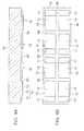
- Each portion in which the first semiconductor layer 11 is exposed does not include the light emitting layer 13 as shown in FIG. 4A .
- An area of the second semiconductor layer 12 that includes the light emitting layer 13 is wider than an area of the portion not including the light emitting layer 13, where the first semiconductor layer 11 is exposed, as shown in FIG. 4B .
- p-side electrodes 16 and n-side electrodes 17 are formed on the second face of the semiconductor layer 15.
- the p-side electrodes 16 are formed on the surfaces of the second semiconductor layer 12.
- the n-side electrodes 17 are formed on the exposed surfaces of the first semiconductor layer 11.
- the p-side electrodes 16 and the n-side electrodes 17, for example, are formed using a sputtering method, a vapor deposition method, or the like. Either the p-side electrodes 16 or the n-side electrodes 17 may be formed first, or the p-side electrode 16 and n-side electrodes 17 may be simultaneously formed and inevitably made of the same material.
- the p-side electrode 16 has preferably formed so as to reflect the light emitted from the light emitting layer 13.
- the p-side electrode 16 may include silver, silver alloy, aluminum, aluminum alloy, and the like.
- the p-side electrode 16 may include a metal protective film (barrier metal) formed on the reflection electrode, in order to prevent the reflection electrode from the sulfurization and the oxidization.
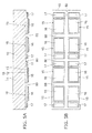
- the area of the p-side electrode 16 provided in the portion including the light emitting layer 13 is wider than the area of the n-side electrode 17 provided in the portion not including the light emitting layer 13. Accordingly, a wide light emitting portion can be obtained. It is noted that the layout of the p-side electrode 16 and the n-side electrode 17 shown in FIG. 5B is one example, and the embodiment is not limited thereto.
- a silicon nitride film or a silicon oxide film may be formed as a passivation film by using a chemical vapor deposition (CVD) method between the p-side electrode 16 and the n-side electrode 17, and on the end face (side surface) of the light emitting layer 13.
- CVD chemical vapor deposition
- activated annealing may be performed as necessary for forming an ohmic contact between each electrode and the semiconductor layer.
- first openings 18a and a second opening 18b are selectively formed in the insulating film 18.
- a plurality of the first openings 18a are formed in the insulating film 18, and each of the first openings 18a reaches the p-side electrodes 16.
- the second opening 18b also reaches the n-side electrode 17.
- an organic material such as a photosensitive polyimide or benzocyclobutene can be used as the material of the insulating film 18.
- the insulating film 18 can be directly exposed and developed using photo-lithography, and the first and second openings 18a, 18b are directly formed therein without using a resist mask.
- an inorganic film such as a silicon nitride film or a silicon oxide film may be used as the insulating film 18.
- the first openings 18a and the second opening 18b are formed using selective etching using a resist mask formed on the insulating film 18.
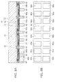
- a metal film 19 is formed on the surface of the insulating film 18, the inner face (the side wall and the bottom portion) of the first opening 18a, and the inner face (the side wall and the bottom portion) of the second opening 18b.
- the metal film 19 is used as a seed metal for plating, as described later.
- the metal film 19 for example, is formed using a sputtering method.
- the metal film 19 includes a stacked film, for example, in which a titanium (Ti) layer and a copper (Cu) layer are stacked in order from the insulating film 18 side.
- a titanium (Ti) layer and a copper (Cu) layer are stacked in order from the insulating film 18 side.
- an aluminum layer may be used instead of the titanium layer.
- resists 91 are selectively formed on the metal film 19, and Cu electroplating is performed using the metal film 19 as a current path.
- a p-side interconnection layer 21 and an n-side interconnection layer 22 are selectively formed on the metal film 19.
- the p-side interconnection layer 21 and the n-side interconnection layer 22 are simultaneously formed, for example, by using copper plating.
- the p-side interconnection layer 21 is also formed inside the first openings 18a and is electrically connected to the p-side electrode 16 via the metal film 19.
- the n-side interconnection layer 22 is formed also inside the second openings 18b and is electrically connected to the n-side electrodes 17 via the metal film 19.
- the resists 91 that are used for plating the p-side interconnection layer 21 and the n-side interconnection layer 22 are removed using solvent or oxygen plasma.
- resists 92 are formed for forming metal pillars.
- the resist 92 is thicker than the above-described resist 91. It may be possible to leave the resists 91 without removing in the previous process, and the resists 92 are formed so as to overlap the resists 91. First openings 92a and second openings 92b are formed in the resists 92.
- a p-side metal pillar 23 and an n-side metal pillar 24 are formed on the p-side interconnection layer 21 and n-side interconnection layer 22 respectively.
- the p-side metal pillar 23 is formed on the p-side interconnection layer 21 inside the first opening 92a that is formed in the resist 92.
- the n-side metal pillar 24 is formed on the n-side interconnection layer 22 inside the second opening 92b that is formed in the resist 92.
- the p-side metal pillar 23 and the n-side metal pillar 24 are simultaneously formed using copper plating, for example.
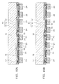
- the resist 92 as shown in FIG. 10A is removed, for example, by using solvent or oxygen plasma. Thereafter, exposed parts of the metal film 19 are removed by wet etching while using the p-side metal pillar 23, the n-side metal pillar 24, the p-side interconnection layer 21, and the n-side interconnection layer 22 as a mask. Accordingly, as shown in FIG. 10B , the p-side interconnection layer 21 and the n-side interconnection layer 22 is separated from each other on the insulating film 18, and the electric connection is cut off therebetween.
- an insulating film 25 is stacked on the insulating film 18.
- the insulating film 25 covers the p-side interconnection layer 21, the n-side interconnection layer 22, the p-side metal pillar 23, and the n-side metal pillar 24.
- the insulating film 25 has an insulating property.
- carbon black may be dispersed in the insulating film 25 so as to shield the light emitted from the light emitting layer 13.
- the substrate 10 is removed as shown in FIG. 11B .
- the substrate 10 can be removed, for example, using a laser lift-off method.
- the substrate 10 can be removed by etching from the first semiconductor layer 11.
- the semiconductor layer 15 is reinforced by the p-side metal pillar 23, the n-side metal pillar 24, and the insulating film 25, and accordingly, the wafer shape can be maintained even after the substrate 10 is removed therefrom.
- laser light is radiated from the backside of the substrate 10 toward the first semiconductor layer 11.
- the laser light has transparency for the substrate 10 and has a wavelength in an absorption band of the first semiconductor layer 11.
- part of the first semiconductor layer 11 that is located near the interface absorbs energy of the laser light and decomposes.
- the first semiconductor layer 11 is decomposed into gallium (Ga) and nitrogen gas. According to the decomposition reaction, a minute gap is formed between the substrate 10 and the first semiconductor layer 11, whereby the substrate 10 and the first semiconductor layer 11 are separated from each other.
- the insulating film 25, and the metal that configures the p-side metal pillar 23 and the n-side metal pillar 24 are more flexible than the material of the semiconductor layer 15. That is, the semiconductor layer 15 is supported by the flexible support members. Accordingly, the released stress may be absorbed by the insulating film 25, the p-side metal pillar 23 and the n-side metal pillar 24, thereby preventing the semiconductor layer 15 from being destroyed.
- the first face 15a of the semiconductor layer 15 is cleaned after removing the substrate 10 therefrom.
- gallium (Ga) that is stuck to the first face 15a is removed by using rare hydrofluoric acid or the like.
- wet etching is performed for the first face 15a, for example, by using a potassium hydroxide (KOH) solution, tetramethylammonium hydroxide (TMAH), or the like.
- KOH potassium hydroxide
- TMAH tetramethylammonium hydroxide
- the concavo-convex is formed on the first face 15a due to a difference in the etching speed that depends on the direction of the crystal plane, as shown in FIG. 12A .
- the concavo-convex may be formed on the first face 15a by etching using a resist mask. The concavo-convex formed on the first face 15a may improve the light extraction efficiency.
- a transparent resin layer 30 is formed on the first face 15a.
- the transparent resin layer 30 is also formed on the insulating film 18 between semiconductor layers 15 adjacent to each other. More specifically, the transparent resin 31 is thermally cured after a transparent resin 31 of a liquid phase in which scattering substances 32 are dispersed is supplied to the upper side of the first face 15a, for example, using a method such as a printing method, a potting method, a molding method, or a compression molding.
- the surface (the lower face in FIG. 12B ) of the insulating film 25 is ground such that the p-side external terminals 23a and the n-side external terminals 24a are exposed as shown in FIG. 13A and FIG. 13B corresponding to the lower face of FIG. 13A .
- the wafer is diced through the transparent resin layer 30, the insulating film 18, and the insulating film 25 so as to separate into a plurality of semiconductor light emitting devices 1.
- the dicing is performed using a dicing blade.
- the dicing may be performed using laser radiation.
- the semiconductor light emitting device 1 may have a single chip structure that includes one semiconductor layer 15 or a multiple-chip structure that includes a plurality of semiconductor layers 15.
- the substrate 10 has been already removed.
- the semiconductor layer 15 is also removed in the groove 80, the semiconductor layer 15 can be prevented from damage, while the dicing is performed.
- the end portion (side surface) of the semiconductor layer 15 is covered with the insulating film 18. Thereby, the protection of the end portion can be obtained without any additional process after dicing into the plurality of semiconductor light emitting devices 1.
- each diced device Since the above-described manufacturing process before dicing are performed in the wafer state, and each diced device includes a package protecting the semiconductor 15 and the interconnection formed therein, it is possible to significantly reduce the production cost. In other words, the interconnection and the packaging are completed at the diced state. Accordingly, it is possible to improve the productivity, and to reduce the manufacturing cost.
- the p-side interconnection layer 21 and the n-side interconnection layer 22 may be directly bonded to the pads of the mounting substrate without providing the p-side metal pillar 23 and the n-side metal pillar 24.
- the p-side interconnection layer 21 and the p-side metal pillar 23 are not limited to be the separately formed ones, and the p-side interconnection may be provided with the p-side interconnection layer 21 and the p-side metal pillar 23, which are formed into a single body in the same process.
- the n-side interconnection layer 22 and the n-side metal pillar 24 are not limited to be the separately formed ones, and the n-side interconnection may be provided with the n-side interconnection layer 22 and the n-side metal pillar 24, which is formed into a single body in the same process.
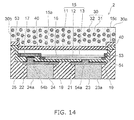
- FIG. 14 is a schematic cross-sectional view of a semiconductor light emitting device 2 according to a second embodiment.
- the semiconductor light emitting device 2 includes a semiconductor layer 15.
- the semiconductor layer 15 includes a first face 15a and a second face 15b opposite to the first face 15a (see FIG. 15 ).
- a transparent resin layer 30 including a scattering substance 32 is provided on the first face 15a.
- an inorganic film 40 is provided between the first face 15a and the transparent resin layer 30.
- electrodes and interconnections are provided on the second face 15b side.
- the semiconductor layer 15 includes a light emitting layer 13, and externally emits light emitted from the light emitting layer 13 from the first face 15a through the inorganic film 40 and the transparent resin 30.
- the second face 15b of the semiconductor layer 15 is processed in a concavo-convex shape.
- a convex portion which is a first portion, includes the light emitting layer 13.
- a p-side electrode 16 is provided on the surface of a second semiconductor layer 12, which is the surface of the convex portion. In other words, the p-side electrode 16 is provided on the second face 15b of the first portion including the light emitting layer 13.
- a second portion not including the light emitting layer 13 is provided side by side with the convex portion on the second face 15b of the semiconductor layer 15.
- An n-side electrode 17 is provided on the surface of a first semiconductor layer 11 of the second portion. Namely, the n-side electrode 17 is provided on the second face 15b of the second portion not including the light emitting layer 13.
- the area of the second semiconductor layer 12 including the light emitting layer 13 is wider than the area of the first semiconductor layer 11 not including the light emitting layer 13.
- the area of the p-side electrode 16 provided on the portion including the light emitting layer 13 is wider than the area of the n-side electrode 17 provided on the portion not including the light emitting layer 13.
- a first insulating film (herein after referred to as an insulating film 54) is provided on the second face 15b side of the semiconductor layer 15.
- the insulating film 54 covers the second face 15b of the semiconductor layer 15, the p-side electrode 16, and the n-side electrode 17.
- the insulating film 54 further covers a side face 15c of the semiconductor layer 15, and contacts the inorganic film 40 at the outer edge of the first face 15a.
- the insulating film 54 is an inorganic film such as a silicon oxide film or a silicon nitride film, for example. Namely, preferably, the semiconductor layer 15 is covered with an inorganic film.
- An insulating film 53 covering the light emitting layer 13 and the side face of the second semiconductor layer 12 (the side face of the convex portion) may be provided between the insulating film 54 and the semiconductor layer 15.
- a p-side interconnection layer 21 and an n-side interconnection layer 22 are provided apart from each other on the face of the insulating film 54 opposite to the second face 15b of the semiconductor layer 15.
- the p-side interconnection layer 21 is electrically connected to the p-side electrode 16 through an opening 54a (a first opening) provided in the insulating film 54.
- the n-side interconnection layer 22 is electrically connected to the n-side electrode 17 through an opening 54b (a second opening) formed in the insulating film 54.
- a p-side metal pillar 23 is provided on the face of the p-side interconnection layer 21 opposite to the p-side electrode 16.
- An n-side metal pillar 24 is provided on the face of the n-side interconnection layer 22 opposite to the n-side electrode 17.
- the n-side interconnection layer 22, the n-side metal pillar 24, and the metal film 19 configure an n-side interconnection in the embodiment.
- An insulating film 25 is provided on the insulating film 54.
- the insulating film 25 is provided between the p-side metal pillar 23 and the n-side metal pillar 24.
- the insulating film 25 covers the periphery of the p-side interconnection and the periphery of the n-side interconnection.
- the side face of the p-side metal pillar 23 and the side face of the n-side metal pillar 24 are covered with the insulating film 25.
- the face of the p-side metal pillar 23 opposite to the p-side interconnection layer 21 is exposed from the insulating film 25, and serves as a p-side external terminal 23a.
- the face of the n-side metal pillar 24 opposite to the n-side interconnection layer 22 is exposed from the insulating film 25, and serves as an n-side external terminal 24a.
- the p-side external terminal 23a and the n-side external terminal 24a are exposed from the same face of the insulating film 25 (in the lower surface in FIG. 14 ), and joined to pads provided on a mounting substrate through a bonding material such as solder, other metals, and a conductive material, for example.
- the configurations of the p-side interconnection and the n-side interconnection are the same as the first embodiment except the number of the openings 54a provided on the insulating layer 54, and may exhibit the similar advantages. Fine concavity and convexity are also formed on the first face 15a of the semiconductor layer 15 by wet etching (frosting) using an alkaline liquid solution for improving the efficiency of extracting light emitted from the light emitting layer 13.
- the transparent resin layer 30 including the scattering substance 32 is provided on the first face 15a, so that the distribution of light can be widened.
- the inorganic film 40 is provided between the first face 15a and the transparent resin layer 30, so that the heat dissipation of the semiconductor layer 15 may be improved.
- the thermal conductivity coefficient of an inorganic film such as a silicon oxide film and a silicon nitride film is greater than the thermal conductivity coefficient of the resin layer. Therefore, the inorganic film 40 is additionally provided between the first face 15a and the transparent resin layer 30, so that heat generated in the light emitting layer 13 can be more efficiently dissipated through the p-side interconnection layer 21 and the n-side interconnection layer 22, for example.
- the inorganic film 40 is provided on the first face 15a, and the insulating film 54 provided on the second face 15b side is an inorganic film, so that the semiconductor layer 15 is covered with the inorganic film. Accordingly, it becomes possible to suppress the penetration of moisture or heavy metal into the semiconductor layer 15, and to improve the reliability of the semiconductor light emitting device 2.
- the inorganic film 40 and the insulating film 54 are formed of silicon nitride films, so as to suppress the migration of metal atoms such as Cu.
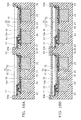
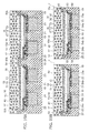
- FIGS. 15A to 19B are partial schematic views illustrating a wafer in the manufacturing process.
- FIG. 15A is a top face view
- FIGS. 15B to 19B are partial cross sections of a wafer in the process.
- FIGS. 15A and 15B show a state in which the p-side electrode 16 and the n-side electrode 17 are formed on the semiconductor layer 15 provided on a substrate 20.
- a silicon substrate is used for the substrate 20.
- the semiconductor layer 15 is formed on the major surface of the substrate 20, including the first semiconductor layer 11, the light emitting layer 13, and the second semiconductor layer 12 stacked in order.
- the second semiconductor layer 12 and the light emitting layer 13 are selectively etched to form a convex portion 16a.
- the insulating film 53 is formed to cover the second face 15b, that is, the top face and side face of the convex portion 16a and the exposed surface of the first semiconductor layer 11.
- the insulating film 53 is a silicon oxide film or a silicon nitride film, for example, and protects the light emitting layer 13 and the second semiconductor layer 12 exposed in the side face of the convex portion 16a.
- the p-side electrode 16 is formed on the top face of the convex portion 16a.
- the p-side electrode 16 contacts the second semiconductor layer 12 through the opening 53a provided in the insulating film 53.
- the n-side electrode 17 is formed on the portion in which the first semiconductor layer 11 is exposed through the opening 53b provided in the insulating film 53.
- the p-side electrode 16 is formed on the second face 15b of the portion including the light emitting layer 13 (i.e. the convex portion), and the n-side electrode 17 is formed on the second face 15b of the portion not including the light emitting layer 13.
- a groove 83 is formed as shown in FIG. 16A .
- the groove 83 penetrates through the insulating film 53 and the semiconductor layer 15, and reaches the substrate 20.
- the groove 83 can be formed by RIE (Reactive Ion Etching) using a resist mask (not shown), for example.
- the groove 83 is formed in a grid configuration, for example, on the substrate 20 in the wafer state, and separates the semiconductor layer 15 into a plurality of chips.
- the substrate 20 is also etched in the groove 83, forming a recess 83a in the major surface of the substrate 20.
- the insulating film 54 is formed so as to cover the semiconductor layer 15, the p-side electrode 16, the n-side electrode 17, and the inside of the groove 83.
- the insulating film 54 covers the side face 15c of the semiconductor layer 15, and fills the recess 83a.
- An inorganic film such as a silicon nitride film or a silicon oxide film is used for the insulating film 54, for example.
- the insulating film 54 is patterned by wet etching, for example, and the first opening 54a and the second opening 54b are selectively formed in the insulating film 54.
- the p-side interconnection layer 21 is formed so as to communicate with the p-side electrode 16 through the first opening 54a and the n-side interconnection layer 22 is formed so as to communicate with the n-side electrode 17 through the second opening 54b.
- the p-side interconnection layer 21 and the n-side interconnection layer 22 are formed by Cu plating using the metal film 19 provided on the insulating film 54 as a seed layer, for example, (see FIG. 6 and FIG. 7 ).
- the p-side metal pillar 23 and the n-side metal pillar 24 are formed on the p-side interconnection layer 21 and the n-side interconnection layer 22, respectively.
- the p-side metal pillar 23 and the n-side metal pillar 24 are also formed by Cu plating using the metal film 19 as a seed layer, for example, (see FIG. 8 to FIG. 10 ).
- the insulating film 25 is stacked on the insulating film 54.
- the insulating film 25 is a resin covering the p-side interconnection layer 21, the n-side interconnection layer 22, the p-side metal pillar 23, and the n-side metal pillar 24, for example.
- the insulating film 25 may include carbon black or titanium oxide so as to provide light shielding for light emitted from the light emitting layer 13, for example.
- the substrate 20 is removed by wet etching, for example. Since the semiconductor layer 15 is reinforced by the p-side metal pillar 23, the n-side metal pillar 24, and the insulating film 25, the semiconductor layer 15 can maintain the wafer shape after removing the substrate 20.
- the insulating film 54 filled in the recess 83a of the substrate 20 is left on the first face 15a side as a bank 83b surrounding the outer edge of the semiconductor layer 15.
- the first face 15a of the semiconductor layer 15 from which the substrate 20 is removed is wet-etched in order to form fine concavity and convexity therein.
- the fine concavity and convex may also be formed in the first face 15a using a resist pattern as the etching mask.
- the inorganic film 40 is formed on the first face 15a and the bank 83b.
- the inorganic film 40 is a silicon nitride film formed by sputtering, for example.
- the bank 83b is formed to surely contact the inorganic film 40 with the insulating film 54.
- the surface of the semiconductor layer 15 is covered with the insulating film 54 and the inorganic film 40.
- the transparent resin layer 30 is formed on the inorganic film 40.
- the transparent resin layer 30 is also formed on the bank 83b between the adjacent semiconductor layers 15. More specifically, the liquid transparent resin 31 having the scattering substance 32 dispersed therein is supplied on the first face 15a using a method such as printing, potting, molding, and compression molding, for example, and then the liquid transparent resin 31 is thermally set.
- the surface of the insulating film 25 (the lower surface in FIG. 19A ) is ground to expose the p-side external terminal 23a, which is the end surface of the p-side metal pillar 23, and the n-side external terminal 24a, which is the end surface of the n-side metal pillar 24.
- the insulating film 25, the transparent resin layer 30, and the insulating film 54 are cut along the bank 83b between the adjacent semiconductor layers 15, and the wafer is separated into a plurality of the semiconductor light emitting devices 2.
- the wafer may be cut using a dicing blade, or by applying a laser beam.
- the semiconductor light emitting devices 2 separated into dies may have a single chip structure including one semiconductor layer 15, or may have a multichip structure including a plurality of the semiconductor layers 15.
- a transparent resin layer 30 not including the scattering substance 32 may be provided on the first face 15a of the semiconductor layer 15.
- heat dissipation can be improved by the inorganic film 40, and the migration of moisture and metal atoms into the semiconductor layer 15 can be suppressed.
- a fluorescent body that is excited by light emitted from the light emitting layer 13 may be dispersed in the transparent resin layer 30.
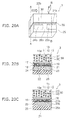
- FIG. 20A is a schematic perspective view of a semiconductor light emitting device 3 according to a third embodiment.
- FIG. 20B is a cross-sectional view taken along line A - A shown in FIG. 20A.
- FIG. 20C is a cross-sectional view taken along line B - B shown in FIG. 20A .
- FIG. 21 is a schematic cross-sectional view of a light emitting module in which the semiconductor light emitting device 3 is mounted on a mounting substrate 200.
- a part of the side surface of the p-side metal pillar 23 is exposed from the insulating film 25 on a third face 25b that has a plane orientation different from the first face 15a and the second face of the semiconductor layer 15.
- the exposed face serves as a p-side external terminal 23b for mounting the semiconductor light emitting device on an external mounting substrate.
- the third face 25b is a face that is approximately perpendicular to the first face 15a and the second face of the semiconductor layer 15.
- the insulating film 25, for example, has four side surfaces of a rectangular shape, and one of the four side surfaces is the third face 25b.
- a part of the side surface of the n-side metal pillar 24 is also exposed from the insulating film 25 on the third face 25b.
- the exposed face serves as an n-side external terminal 24b for mounting the semiconductor light emitting device on the mounting substrate.
- a part of the side surface 21b of the p-side interconnection layer 21 is also exposed in the third face 25b of the insulating film 25 and serves as a p-side external terminal.
- a part of the side surface 22b of the n-side interconnection layer 22 is also exposed in the third face 25b of the insulating film 25 and serves as an n-side external terminal.
- Parts of the p-side metal pillar 23 other than the p-side external terminal 23b that is exposed in the third face 25b is covered with the insulating film 25.
- parts of the n-side metal pillar 24 other than the n-side external terminal 24b that is exposed in the third face 25b is covered with the insulating film 25.
- parts of the p-side interconnection layer 21 other than the side surface 21b that is exposed in the third face 25b is covered with the insulating film 25.
- parts of the n-side interconnection layer 22 other than the side surface 22b that is exposed in the third face 25b is covered with the insulating film 25.
- a transparent resin layer 30 including a scattering substance 32 is provided on the first face 15a.
- An inorganic film 40 may be provided between the first face 15a and the transparent resin layer 30.
- the semiconductor light emitting device 3, as shown in FIG. 21 is mounted in a posture in which the third face 25b faces the mounting face 201 of the mounting substrate 200.
- the p-side external terminal 23b and the n-side external terminal 24b that are exposed in the third face 25b are bonded to the pad 202 that is formed on the mounting face 201 through soldering 203.
- an interconnection pattern is formed on the mounting face 201 of the mounting substrate 200, and the pad 202 is connected to the interconnection pattern.
- the third face 25b is approximately perpendicular to the first face 15a that is the major light emitting face. Accordingly, in the posture in which the third face 25b is disposed toward the lower side, i.e. facing the mounting face 201 side, the first face 15a faces in the horizontal direction, not the upper side of the mounting face 201.
- the semiconductor light emitting device 3 is a so-called side view type device in which light is emitted in the horizontal direction in a case where the mounting face 201 is set as the horizontal plane.
- the transparent resin layer 30 including the scattering substance 32 provided on the first face 15a increases the radiation angle of light, and the distribution of light can be widened.
- FIG. 22A and FIG. 22B are schematic views of a light source unit 100 according to a fourth embodiment.
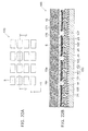
- FIG. 22A is a plan view illustrating an arrangement of semiconductor light emitting devices mounted on a mounting substrate 150.
- FIG. 22B is a cross-sectional view along a line C-C in FIG. 22B .
- the light source unit 100 includes a mounting substrate 150, a plurality of semiconductor light emitting devices 5 mounted on the mounting substrate 150, a first resin layer (herein after referred to as a resin layer 160) covering the semiconductor light emitting devices 5 and the mounting substrate 150, and a second resin layer provided on the first resin layer (herein after referred to as a resin layer 170).
- a resin layer 160 a first resin layer covering the semiconductor light emitting devices 5 and the mounting substrate 150
- a second resin layer provided on the first resin layer herein after referred to as a resin layer 170.
- the mounting substrate 150 includes a metal base 101, an insulating layer 102 provided on the metal base 101, and a plurality of interconnections 103 provided on the insulating layer 102, for example.
- the mounting substrate 150 includes a solder resist 107 covering the interconnections 103 and the insulating film 102.
- the semiconductor light emitting device 5 includes a semiconductor layer 15, an insulating layer 18 covering the semiconductor layer 15, and an insulating layer 25 provided on the insulating layer 18, for example.
- the semiconductor layer 15 has a first face 15a and a second face 15b opposite to the first face 15a, and includes an semiconductor layer 11, a light emitting layer 13, and a semiconductor layer 12 (see FIG. 1 ).
- the semiconductor device 5 includes a p-side electrode 16 and an n-side electrode 17.
- the p-side electrode 16 is provided on the portion of the semiconductor layer 15 including the light emitting layer 13 on the second face 15b side.
- the n-side electrode 17 is provided on the portion of the semiconductor layer 15 not including the light emitting layer 13 on the second face 15b side.
- the semiconductor device 5 further includes the insulating film 18, the p-side interconnection, the n-side interconnection, and the insulating film 25.
- the insulating film 18 covers the semiconductor layer 15, the p-side electrode 16, and the n-side electrode 17.
- the p-side interconnection and the n-side interconnection are provided on the insulating film 18.
- the p-side interconnection is electrically connected to the p-side electrode 16 through an opening 18a provided on the insulating film 18.
- the n-side interconnection is electrically connected to the n-side electrode 17 through an opening 18b provided on the insulating film 18.
- the insulating film 25 is provided on the insulating film 18 between the p-side interconnection and the n-side interconnection.
- the p-side interconnection includes a p-side interconnection layer 21 connected to the p-side electrode 16 and a p-side metal pillar 23 provided on the p-side interconnection layer 21.
- the n-side interconnection includes an n-side interconnection layer 22 connected to the n-side electrode 17 and an n-side metal pillar 24 provided on the n-side interconnection layer 22.
- the semiconductor device 5 is mounted in such a way that the second face 15b faces the mounting substrate 150.
- the p-side interconnection and the n-side interconnection are connected to the interconnections 103 through a solder 105.
- the p-side metal pillar 23 and the n-side metal pillar 24 exposed from the insulating layer 25 are connected to the interconnections 103.
- the semiconductor device 5 is electrically connected to an external driver through the interconnections 103.
- the p-side interconnection and the n-side interconnection of the adjacent semiconductor devices 5 are connected to each other with a single interconnection 103, and a plurality of the semiconductor devices 5 are connected to each other in series.
- the resin layer 160 covers the first face 15a and side face of the semiconductor device 5 and the surface of the mounting substrate 150 between the adjacent semiconductor devices 5.
- the resin layer 160 transmits light emitted from the light emitting layer 13, which is radiated on the first face side.
- the resin layer 170 includes a fluorescent substance 171 that is excited by light emitted from the light emitting layer 13 and emits light having a different wavelength from the wavelength of the exciting light.
- the resin layer 170 transmits light emitted from the light emitting layer 13 and the light emitted from the fluorescent substance 171.
- the semiconductor light emitting devices 5 are disposed on the mounting substrate 150 in a matrix configuration, for example. Namely, as shown in FIG. 22A , the semiconductor light emitting devices 5 are provided side by side with an equal distance in a first direction (in an X-direction) on the mounting substrate 150 and in a second direction (in a Y-direction) orthogonal to the first direction.
- the light source unit 100 includes the semiconductor devices 5 thus disposed, and operates as a surface light source by simultaneously emitting light from the semiconductor devices 5 through the interconnections 103, for example.
- the resin layer 170 including the fluorescent body 171 is provided on the resin layer 160 covering the semiconductor devices 5 and the mounting substrate 150, so that the surface light source can be implemented, which suppresses color shading and uniformly of the light emission.
- the resin layer 160 includes a flat surface absorbing the irregularity of the mounting substrate 150 on which the semiconductor devices 5 are mounted. Thereby, the fluorescent body 171 is uniformly distributed in the XY plane in the resin layer 170 provided on the resin layer 160.
- the refractive index of the resin layer 160 is preferably greater than the refractive index of the insulating layer 18 covering the side face of the semiconductor layer 15. Namely, the total reflection on the interface between the insulating layer 18 and the resin layer 160 can be suppressed, and light emitted from the side face of the semiconductor light emitting device 5 can be made uniform.
- FIGS. 23A and 23B are schematic cross-sectional views of light source units 110 and 120 according to variations of the fourth embodiment.
- the light source unit 110 shown in FIG. 23A includes the mounting substrate 150, a plurality of the semiconductor devices 5 mounted on the mounting substrate 150, the resin layer 180 covering the semiconductor light emitting devices 5 and the mounting substrate 150, and the resin layer 170 provided on the resin layer 180.
- the resin layer 180 transmits light emitted from the light emitting layer 13.
- the resin layer 180 includes a scattering substance 181 that scatters light emitted from the light emitting layer 13. Thereby, the light emitted from the semiconductor light emitting devices 5 is made uniform, and the distribution of light can be widened.
- the resin layer 180 filled between the adjacent semiconductor light emitting devices 5 scatters light emitted from the side faces of the semiconductor light emitting devices 5, and reduces optical interference between the lights emitted from the adjacent light emitting devices. Accordingly, fluctuations of light emission in the light source unit 110 are suppressed, thereby implementing uniform surface emission.
- the light source unit 120 shown in FIG. 23B includes the mounting substrate 150, a plurality of the semiconductor devices 5 mounted on the mounting substrate 150, the resin layer 160 covering the semiconductor light emitting devices 5, a third resin layer (hereinafter referred to as a resin layer 190) filled on a substrate between the adjacent semiconductor light emitting devices 5, and the resin layer 170 provided on the resin layers 160 and 190.
- the resin layer 190 is provided between the resin layers 160 covering the semiconductor light emitting devices 5 in an island shaped arrangement.
- the resin layer 190 includes a phosphor material having a longer light emission period than the fluorescent substance 171 included in the resin layer 170.
- a metal complex such as iridium complex can be used for the phosphor material, for example.
- fluctuations of light emission can be reduced in the light source unit 120.
- the light source unit 110 is directly driven with a commercial power supply of 50 Hz or 60 Hz
- flickers of the light emission is induced corresponding to the power supply frequency.
- light is continuously emitted from the phosphor material included in the resin layer 190. Accordingly, the flickers in the light source unit 120, that is, fluctuations of light emission with over time can be suppressed.
- FIG. 24A and FIG. 24B are schematic plan views of light source units 130 and 140 according to other variations of the fourth embodiment.
- the light source unit 130 shown in FIG. 24A includes a plurality of the semiconductor light emitting devices 5 disposed on the mounting substrate 150 in a staggered configuration. Namely, the semiconductor light emitting devices 5 are provided side by side with an equal distance in the X-direction. The semiconductor light emitting devices 5 are arranged in such a way that the phases of arrangement in the X-direction are alternately shifted in the Y-direction. Thus, it becomes possible to suppress the fluctuations of the light emission in the semiconductor light emitting devices 5, since the regularity of radiant points is disturbed in this arrangement. It is also possible to suppress the mutual interference of light horizontally emitted from the semiconductor light emitting devices 5.
- the distance between the adjacent semiconductor light emitting devices 5 is made wider than the distance in FIG. 24A .
- the distances between the semiconductor light emitting devices 5 in the X-direction and the Y-direction are made wider than the size of the semiconductor light emitting device 5 in the X-direction and the Y-direction respectively.
- the distance between the adjacent semiconductor light emitting devices 5 is provided wider than the size of the semiconductor light emitting device 5 in any arrangement directions on the mounting substrate 150. Thereby, the heat of the semiconductor light emitting devices 5 can be efficiently dissipated through the mounting substrate 150.
- the light source unit 140 includes the resin layer 180 covering the semiconductor light emitting devices 5 and the resin layer 170 provided on the resin layer 180. Namely, the scattering substance 181 is dispersed in the resin layer covering the semiconductor light emitting devices 5, so that the distribution of light of the semiconductor light emitting devices 5 can be widened. Accordingly, fluctuations of light emission in the light source unit 140 can be suppressed even though the semiconductor light emitting device 5 is disposed with a wider distance.
- FIG. 25 is a schematic cross-sectional view of a semiconductor light emitting device 6 according to a variation of the fourth embodiment.
- the semiconductor light emitting device 6 is mounted on the mounting substrate 150 instead of the semiconductor light emitting device 5.
- the semiconductor light emitting device 6 includes the semiconductor layer 15.
- the semiconductor layer 15 includes the first face 15a and the second face 15b opposite to the first face 15a, and includes the semiconductor layer 11, the light emitting layer 13, and the semiconductor layer 12.
- the semiconductor device 6 includes the p-side electrode 16 and the n-side electrode 17 on the second face 15b side of the semiconductor layer 15.
- the p-side electrode 16 is provided on the portion of the semiconductor layer 15 including the light emitting layer 13.
- the n-side electrode 17 is provided on the portion of the semiconductor layer 15 not including the light emitting layer 13.
- a p-side pad 41 and a n-side pad 42 are provided on the p-side electrode 16 and the n-side electrode 17 respectively.
- the semiconductor device 6 further includes an insulating film 38, the p-side interconnection, the n-side interconnection, and the insulating film 33.
- the insulating film 38 covers the semiconductor layer 15, the p-side pad 41 and the n-side pad 42.
- the p-side interconnection and the n-side interconnection are provided on the insulating film 38.
- the p-side interconnection is electrically connected to the p-side electrode 16 through an opening 38a provided in the insulating film 38.
- the n-side interconnection is electrically connected to the n-side electrode 17 through an opening 38b provided in the insulating film 38.
- the p-side interconnection includes a p-side interconnection layer 21 connected to the p-side pad 41 and a p-side metal pillar 23 provided on the p-side interconnection layer 21.
- the n-side interconnection includes an n-side interconnection layer 22 connected to the n-side pad 42 and an n-side metal pillar 24 provided on the n-side interconnection layer 22.
- the n-side interconnection layer 22 includes a portion 39 extending so as to cover the side face of the semiconductor layer 15.
- the p-side interconnection layer 21 covers the insulating film 38 and the p-side pad 41.
- the n-side interconnection layer 22 covers the insulating film 38, the n-side pad 42 and a side face 15c of the semiconductor layer 15.
- the p-side interconnection layer 21 and the n-side interconnection layer 22 are formed by Cu electric field plating.
- the insulating film 33 is provided between the p-side interconnection and the n-side interconnection, and covers the p-side interconnection layer 21, the n-side interconnection layer 22, the side face of the p-side metal pillar 23 and the side face of the n-side metal pillar 24.
- an insulating layer 40 is provided on the first face side of the semiconductor layer 15.
- an inorganic film such as a silicon oxide film and like may be used for the insulating layer 40.
- a resin layer that transmits the light emitted from the light emitting layer 13 may also be used for the insulating layer 40.
- the semiconductor light emitting device may have a structure without the insulating layer 40.
- the extending portion 39 of the n-side interconnection layer 22 covers the side face of the semiconductor layer 15. Thereby, light emitted from the side face is suppressed in the semiconductor light emitting device 6. Therefore, when a plurality of the semiconductor light emitting devices 6 are mounted on the mounting substrate 150, it becomes possible to suppress interference between the lights emitted from the side faces of the semiconductor light emitting devices 6. Namely, using the semiconductor light emitting device 6 may suppress the fluctuations of the light emission, and implements a surface light source with uniform light emission.
Landscapes
- Led Device Packages (AREA)
- Led Devices (AREA)
- Engineering & Computer Science (AREA)
- Microelectronics & Electronic Packaging (AREA)
Abstract
Description
- Embodiments are related generally to a semiconductor light emitting device and a light source unit.
- A semiconductor light emitting device is a light source of low power consumption and long lifetime, and is being used for various applications. The semiconductor light emitting device can be downsized, thereby being accommodated in a small chip size package. However, it becomes more difficult to control the light distribution of the semiconductor light emitting device as the package size becomes smaller.
-
-
FIG. 1 is a schematic cross-sectional view illustrating a semiconductor light emitting device according to a first embodiment; -
FIGS. 2A to 13B are schematic views illustrating a manufacturing process of the semiconductor device according to the first embodiment; -
FIG. 14 is a schematic cross-sectional view illustrating a semiconductor light emitting device according to a second embodiment; -
FIGS. 15A to 19B are schematic views illustrating a manufacturing process of the semiconductor device according to the second embodiment; -
FIGS. 20A to 20C are schematic views illustrating a semiconductor device according to a third embodiment; -
FIG. 21 is a schematic cross-sectional view illustrating the semiconductor device according to the third embodiment, wherein the device is mounted on a substrate; -
FIGS. 22A and 22B are schematic views illustrating a light source unit according to a fourth embodiment; -
FIGS. 23A and 23B are schematic cross-sectional views illustrating light source units according to variations of the fourth embodiment; -
FIGS. 24A and 24B are schematic plan views illustrating light source units according to other embodiments of the fourth embodiment; and -
FIG. 25 is a schematic cross-sectional view illustrating a semiconductor light emitting device according to a variation of the fourth embodiment. - According to an embodiment, a semiconductor light emitting device includes a semiconductor layer, a p-side electrode, n-side electrode and a resin layer. The semiconductor layer has a first face and a second face opposite to the first face, and includes a light emitting layer. The p-side electrode is provided on the semiconductor layer on the second face side. The n-side electrode is provided on the semiconductor layer on the second face side. The resin layer is provided on the first face and transmits light emitted from the light emitting layer, the resin layer including a top surface opposite to the first face and four side faces provided along an outer edge of the first face and connected to the top surface, the resin layer including a scattering substance scattering the light emitted from the light emitting layer.
- Embodiments will be described with reference to the drawings. Like reference numerals in the drawings denote like elements, and the descriptions of the like elements are appropriately omitted and the different elements are described.
-
FIG. 1A is a schematic cross-sectional view of a semiconductorlight emitting device 1 according to a first embodiment. The semiconductorlight emitting device 1 includes asemiconductor layer 15 having alight emitting layer 13. Thesemiconductor layer 15 includes afirst face 15a and asecond face 15b opposite to thefirst face 15a (seeFIG. 2A ), and electrodes and interconnections are provided on thesecond face 15b side. Thesemiconductor layer 15 externally emits light from thefirst face 15a, which is emitted from thelight emitting layer 13. - The
semiconductor layer 15 includes afirst semiconductor layer 11 and asecond semiconductor layer 12. Thefirst semiconductor layer 11 and thesecond semiconductor layer 12, for example, contain gallium nitride. Thefirst semiconductor layer 11 may include an underlying buffer layer, an n-type GaN layer, and the like. Thesecond semiconductor layer 12 includes a p-type GaN layer, a light emitting layer (active layer) 13, and the like. Thelight emitting layer 13 may include a material that emits blue light, purple light, blue-purple light, ultraviolet light, or the like. Thesemiconductor layer 15 includes a first portion including thelight emitting layer 13, and a second portion not including thelight emitting layer 13. - The semiconductor
light emitting device 1 further includes a resin layer (hereinafter referred to as a transparent resin layer 30) provided on thefirst face 15a. Thetransparent resin layer 30 includes atransparent resin 31 that transmits light emitted from thelight emitting layer 13 and a scatteringsubstance 32 dispersed in thetransparent resin 31. Thescattering substance 32 is a fine particle having a refractive index different from the refractive index of thetransparent resin 31. The grain size of the scatteringsubstance 32 is smaller than the wavelength of light emitted from thelight emitting layer 13. - It is noted that "being transparent" referred here is not limited to transmitting all the light emitted from the
light emitting layer 13. Thetransparent resin 31 may partially absorb light emitted from thelight emitting layer 13. "The grain size" is the average grain size, and can be measured with the scanning electron microscope, for example. Next, the structure of the semiconductorlight emitting device 1 will be described in detail with reference toFIG. 1 . - As shown in
FIG. 1 , thesemiconductor layer 15 has a portion including thelight emitting layer 13, and a portion not including thelight emitting layer 13. The area of the portion including thelight emitting layer 13 is provided wider than the area of the portion not including thelight emitting layer 13. - Namely, the
second face 15b of thesemiconductor layer 15 is processed in a concavo-convex shape. The convex portion includes thelight emitting layer 13, and a p-side electrode 16 is provided on the surface of thesecond semiconductor layer 12, which is the surface of the convex portion. In other words, the p-side electrode 16 is provided on thesecond face 15b in the portion including thelight emitting layer 13. - On the
second face 15b of thesemiconductor layer 15, the portion not including thelight emitting layer 13 is provided side by side with the convex portion. An n-side electrode 17 is provided on thefirst semiconductor layer 11 in the portion not including thelight emitting layer 13. Namely, the n-side electrode 17 is provided on thesecond face 15b of the portion not including thelight emitting layer 13. - A first insulating film (hereinafter referred to as an insulating film 18) is provided on the second face side of the
semiconductor layer 15. Theinsulating film 18 covers thesemiconductor layer 15, the p-side electrode 16, and the n-side electrode 17. In addition, theinsulating film 18 covers the side surfaces of thelight emitting layer 13 and thesecond semiconductor layer 12 for the protection thereof. - It is noted that in the specification, "covering" is not limited to the case where a component covering an element directly contacts the element being covered. "Covering" also includes the case where a component covering an element contacts the element being covered via a different component.
- In addition, another insulating film (for example, a silicon oxide film) may be provided between the insulating
film 18 and thesemiconductor layer 15. The insulatingfilm 18, for example, is formed of a resin, such as polyimide that is superior for the patterning of fine openings. Alternatively, an inorganic film such as a silicon oxide film or a silicon nitride film may be used as the material of the insulatingfilm 18. The insulatingfilm 18 covers aside face 15c provided between thefirst face 15b and the second face. The insulatingfilm 18 does not cover thefirst face 15a. - A p-
side interconnection layer 21 and an n-side interconnection layer 22 are provided on a face of the insulatingfilm 18 opposite to the second face of thesemiconductor layer 15, so as to be separated from each other. - Parts of the p-
side interconnection layer 21 are provided in a plurality offirst openings 18a that are formed in the insulatingfilm 18 up to the p-side electrodes 16, and the p-side interconnection layer 21 is electrically connected to the p-side electrodes 16 via the parts provided in thefirst openings 18a. A part of the n-side interconnection layer 22 is also provided in asecond opening 18b that is formed in the insulatingfilm 18 up to the n-side electrodes 17, and the n-side interconnection layer 22 is electrically connected to the n-side electrodes 17. - A p-
side metal pillar 23 is provided on a face of the p-side interconnection layer 21 opposite to the p-side electrode 16. Then, a p-side interconnection includes the p-side interconnection layer 21, the p-side metal pillar 23, and ametal film 19 that serves as a seed layer, as described later. - It should be noted that the
metal film 19 might be undistinguishable, when the same material as the p-side interconnection layer 21 and the n-side interconnection layer 22 is used, and themetal film 19 and each interconnection layer are joined into one body. Themetal film 19 may not be provided in the case where the p-side interconnection layer 21 and the n-side interconnection layer 22 are formed by a method other than the plating method. - An n-
side metal pillar 24 is provided on a face of the n-side interconnection layer 22 opposite to the n-side electrodes 17. Then, an n-side interconnection includes the n-side interconnection layer 22, the n-side metal pillar 24, and themetal film 19. - An insulating
film 25 serving as a second insulating film is stacked on the insulatingfilm 18. The insulatingfilm 25 covers the periphery of the p-side interconnection and the periphery of the n-side interconnection. For example, the side surfaces of the p-side metal pillar 23 and the n-side metal pillar 24 are covered with the insulatingfilm 25. - A face of the p-
side metal pillar 23 opposite to the p-side interconnection layer 21 is exposed from the insulatingfilm 25 and serves as a p-sideexternal terminal 23a. A face of the n-side metal pillar 24 opposite to the n-side interconnection layer 22 is exposed from the insulatingfilm 25 and serves as an n-sideexternal terminal 24a. The p-sideexternal terminal 23a and the n-sideexternal terminal 24a are exposed from the same face of the insulating film 25 (the lower surface inFIG. 1 ). The p-sideexternal terminal 23a and the n-sideexternal terminal 24a are bonded to a pad formed in a mounting substrate through a bonding member such as a solder, other metal, a material having conductivity, or the like. - A distance between the p-side
external terminal 23a and the n-sideexternal terminal 24a is longer than a distance between the p-side interconnection layer 21 and the n-side interconnection layer 22 on the insulatingfilm 18. The p-sideexternal terminal 23a and the n-sideexternal terminal 24a are separated from each other with such a distance, so that the external terminals do not form a short circuit via solder or the like at the time of being mounted on the mounting substrate. - On the other hand, the p-
side interconnection layer 21 may approach the n-side interconnection layer 22 up to a process limit. Accordingly, it is possible to make the area of the p-side interconnection layer 21 wider, and thereby, the contact area can be enlarged between the p-side interconnection layer 21 and the p-side electrode 16. Then it becomes possible to reduce a current density in the p-side interconnection, and to improve the heat dissipation. - Furthermore, the area of the p-
side interconnection layer 21 that is in contact with the p-side electrodes 16 through the plurality offirst openings 18a is larger than the area of the n-side interconnection layer 22 that is in contact with the n-side electrodes 17 through thesecond openings 18b. Thereby, the current density injected into the light emitting layer can be reduced, and the current distribution in thelight emitting layer 13 becomes uniform. In addition, the heat dissipation from thelight emitting layer 13 through the p-side interconnection can be improved. - A high optical output can be acquired, since the
light emitting layer 13 is formed over the first region that is larger than the second region on which the n-side electrode 17 is provided. In addition, the n-side interconnection layer 22 having a larger area than the n-side electrode 17 can be provided on the mounting face side. Accordingly, in the n-side interconnection layer 22, the portion extending on the insulatingfilm 18 can be formed to have larger area than the contact portion that is in contact with the n-side electrodes 17. - The
first semiconductor layer 11 is electrically connected to the n-side metal pillar 24 having the n-sideexternal terminal 24a through the n-side electrode 17, themetal film 19, and the n-side interconnection layer 22. Thesecond semiconductor layer 12 including thelight emitting layer 13 is electrically connected to the p-side metal pillar 23 having the p-sideexternal terminal 23a through the p-side electrode 16, themetal film 19, and the p-side interconnection layer 21. - The p-
side metal pillar 23 is thicker than the p-side interconnection layer 21, and the n-side metal pillar 24 is thicker than the n-side interconnection layer 22. Each thickness of the p-side metal pillar 23, the n-side metal pillar 24, and the insulatingfilm 25 is larger than that of thesemiconductor layer 15. Here, the "thickness" represents a thickness in the vertical direction inFIG. 1 . - In addition, each thickness of the p-
side metal pillar 23 and the n-side metal pillar 24 is larger than that of a stacked body that includes thesemiconductor layer 15, the p-side electrode 16, the n-side electrode 17, and the insulatingfilm 18. In addition, the aspect ratio (the ratio of the thickness to the planar size) of each one of themetal pillars metal pillars metal pillars - According to the embodiment, even though a
substrate 10 used for forming thesemiconductor layer 15 is removed as described later, the mechanical strength of the semiconductorlight emitting device 1 can be maintained, since thesemiconductor layer 15 is stably supported by the p-side metal pillar 23, the n-side metal pillar 24, and the insulatingfilm 25. - Copper, gold, nickel, silver, and the like can be used as the materials of the p-
side interconnection layer 21, the n-side interconnection layer 22, the p-side metal pillar 23, and the n-side metal pillar 24. Among these materials, copper is superior to the other materials in thermal conductivity, resistance for migration, and adhesiveness to the insulatingfilms - The insulating
film 25 reinforces the p-side metal pillar 23 and the n-side metal pillar 24. It is preferable that the thermal expansion coefficient of the insulatingfilm 25 is the same as or closes to the thermal expansion coefficient of the mounting substrate. As examples of such an insulatingfilm 25, there are an epoxy resin, a silicone resin, a fluorine resin, and the like. - In addition, when the semiconductor
light emitting device 1 is mounted on the mounting substrate through the p-sideexternal terminal 23a and the n-sideexternal terminal 24a, the stress applied to thesemiconductor layer 15 through soldering or the like can be absorbed and relieved by the p-side metal pillar 23 and the n-side metal pillar 24. - The p-side interconnection that includes the p-
side interconnection layer 21 and the p-side metal pillar 23 is connected to the p-side electrode 16 through a plurality ofvias 21a that are provided inside the plurality offirst openings 18a and are separated from each other. Accordingly, the p-side interconnection may make stress relieving more effective. - Alternatively, the p-
side interconnection layer 21 may be connected to the p-side electrode 16 through a post that is larger in the planar size than the via 21a. In such a case, the heat dissipation of thelight emitting layer 13 can be improved through the p-side electrode 16, the p-side interconnection layer 21, and the p-side metal pillar 23, all of which are formed of metal. - As described later, the
substrate 10 used for a crystal growth of thesemiconductor layer 15 is removed from thefirst face 15a. Accordingly, the semiconductorlight emitting device 100 can be formed with lower height. - A fine concavo-convex is formed on the
first face 15a of thesemiconductor layer 15 using wet etching (frost process), where an alkali-based solution is applied to thefirst face 15a. The light emitted from thelight emitting layer 13 can be extracted outside through thefirst face 15a, suppressing light reflection at various incident angles by providing the concavo-convex on thefirst face 15a. - A
fluorescent substance layer 30 is provided on thefirst face 15a. Thefluorescent substance layer 30 includes atransparent resin 31 and a plurality offluorescent substances 32 dispersed in thetransparent resin 31. Thetransparent resin 31 has transparency for the lights emitted from thelight emitting layer 13 and thefluorescent substance 32. For example, a silicone resin, an acrylic resin, a phenyl resin, or the like may be used as thetransparent resin 31. - For the scattering
substance 32, a fine particle such as silica and titanium oxide can be used, for example. - Light emitted from the
light emitting layer 13 is scattered in thetransparent resin layer 30 with the scatteringsubstance 32. Since the grain size of the scatteringsubstance 32 is smaller than the peak wavelength of light emitted from thelight emitting layer 13, the emitted light is scattered in Rayleigh's model, and distributed isotropically. - The
transparent resin layer 30 includes atop surface 30a opposite to thefirst face 15a and four side faces 30b connected to thetop surface 30a. The four side faces are provided by cutting together with the insulatingfilms semiconductor layer 15. Light emitted from thelight emitting layer 13 is scattered by the scatteringsubstance 32, and externally emitted from thetop surface 30a and the four side faces (30b). Namely, thetransparent resin layer 30 including the scatteringsubstance 32 can widen the distribution of light emitted from thelight emitting layer 13. - For example, the semiconductor light emitting device exhibits the light distribution in which the luminance in the upward direction perpendicular to the light emitting face becomes higher and the luminance in the lateral direction along the light emitting face is relatively lower as the package size becomes smaller. In the embodiment, the
first face 15a serves as the light emitting face, and thetransparent resin layer 30 provided thereon with the scatteringsubstance 32 makes the luminance in the lateral direction higher. , Hence, the characteristics of wide light distribution can be implemented at low costs in a small chip size package. - Next, a method of manufacturing the semiconductor
light emitting device 1 according to the embodiment will be described with reference toFIGS. 2A to 15B .FIGS. 2A to 13B show partial areas of a wafer. -
FIG. 2A is a schematic cross-sectional view of thesemiconductor layer 15. Thesemiconductor layer 15 is a stacked body including afirst semiconductor layer 11 and asecond semiconductor layer 12, and formed on a major face (the lower face inFIG. 2A ) of asubstrate 10.FIG. 2B is a schematic view corresponding to a lower face inFIG. 2A . - The
first semiconductor layer 11 is formed on the major face of thesubstrate 10, and thesecond semiconductor layer 12 including alight emitting layer 13 is formed thereon. For example, thefirst semiconductor layer 11 and thesecond semiconductor layer 12 may contain gallium nitride, and grown on a sapphire substrate by using a metal organic chemical vapor deposition (MOCVD) method. Alternatively, a silicon substrate may be used as thesubstrate 10. - A
first face 15a of thesemiconductor layer 15 is a face through which thefirst semiconductor layer 11 is in contact with thesubstrate 10, and asecond face 15b of thesemiconductor layer 15 is the surface of thesecond semiconductor layer 12 opposite to thefirst semiconductor layer 11, as shown inFIG. 2 . - Next, as shown in
FIG. 3A , agroove 80 is formed passing through thesemiconductor layer 15 and reaching thesubstrate 10, for example, by using a reactive ion etching (RIE) method using a resist mask (not shown). As shownFIG. 3B corresponding to the lower face ofFIG. 3A , thegroove 80 is formed, for example, in a lattice pattern on thesubstrate 10, and separates thesemiconductor layer 15 into a plurality of chips on thesubstrate 10. - Alternatively, the process for separating the
semiconductor layer 15 into multiple parts may be performed after selectively removing thesecond semiconductor layer 12, or after forming the p-side electrode 16 and the n-side electrode. - Next, as shown in
FIG. 4A and FIG. 4B corresponding to the lower face ofFIG. 4A , parts of thesecond semiconductor layer 12 are removed so as to expose parts of thefirst semiconductor layer 11, for example, by using the RIE method using a resist mask (not shown). - Each portion in which the
first semiconductor layer 11 is exposed does not include thelight emitting layer 13 as shown inFIG. 4A . An area of thesecond semiconductor layer 12 that includes thelight emitting layer 13 is wider than an area of the portion not including thelight emitting layer 13, where thefirst semiconductor layer 11 is exposed, as shown inFIG. 4B . - Next, as shown in
FIG. 5A and FIG. 5B corresponding to the lower face ofFIG. 5A , p-side electrodes 16 and n-side electrodes 17 are formed on the second face of thesemiconductor layer 15. The p-side electrodes 16 are formed on the surfaces of thesecond semiconductor layer 12. The n-side electrodes 17 are formed on the exposed surfaces of thefirst semiconductor layer 11. - The p-
side electrodes 16 and the n-side electrodes 17, for example, are formed using a sputtering method, a vapor deposition method, or the like. Either the p-side electrodes 16 or the n-side electrodes 17 may be formed first, or the p-side electrode 16 and n-side electrodes 17 may be simultaneously formed and inevitably made of the same material. - The p-
side electrode 16 has preferably formed so as to reflect the light emitted from thelight emitting layer 13. Hence, the p-side electrode 16 may include silver, silver alloy, aluminum, aluminum alloy, and the like. In addition, the p-side electrode 16 may include a metal protective film (barrier metal) formed on the reflection electrode, in order to prevent the reflection electrode from the sulfurization and the oxidization. - The area of the p-
side electrode 16 provided in the portion including thelight emitting layer 13 is wider than the area of the n-side electrode 17 provided in the portion not including thelight emitting layer 13. Accordingly, a wide light emitting portion can be obtained. It is noted that the layout of the p-side electrode 16 and the n-side electrode 17 shown inFIG. 5B is one example, and the embodiment is not limited thereto. - In addition, a silicon nitride film or a silicon oxide film may be formed as a passivation film by using a chemical vapor deposition (CVD) method between the p-
side electrode 16 and the n-side electrode 17, and on the end face (side surface) of thelight emitting layer 13. In addition, activated annealing may be performed as necessary for forming an ohmic contact between each electrode and the semiconductor layer. - Next, after all the parts formed on the major face of the
substrate 10 are covered with an insulatingfilm 18 shown inFIG. 6A , and the insulatingfilm 18 is patterned, for example, by using wet etching, wherebyfirst openings 18a and asecond opening 18b are selectively formed in the insulatingfilm 18. A plurality of thefirst openings 18a are formed in the insulatingfilm 18, and each of thefirst openings 18a reaches the p-side electrodes 16. Thesecond opening 18b also reaches the n-side electrode 17. - For example, an organic material such as a photosensitive polyimide or benzocyclobutene can be used as the material of the insulating
film 18. In such a case, the insulatingfilm 18 can be directly exposed and developed using photo-lithography, and the first andsecond openings - Alternatively, an inorganic film such as a silicon nitride film or a silicon oxide film may be used as the insulating
film 18. In a case where the insulatingfilm 18 is an inorganic film, thefirst openings 18a and thesecond opening 18b are formed using selective etching using a resist mask formed on the insulatingfilm 18. - Next, as shown in
FIG. 6B , ametal film 19 is formed on the surface of the insulatingfilm 18, the inner face (the side wall and the bottom portion) of thefirst opening 18a, and the inner face (the side wall and the bottom portion) of thesecond opening 18b. Themetal film 19 is used as a seed metal for plating, as described later. - The
metal film 19, for example, is formed using a sputtering method. Themetal film 19 includes a stacked film, for example, in which a titanium (Ti) layer and a copper (Cu) layer are stacked in order from the insulatingfilm 18 side. Alternatively, an aluminum layer may be used instead of the titanium layer. - Next, as shown in
FIG. 6C , resists 91 are selectively formed on themetal film 19, and Cu electroplating is performed using themetal film 19 as a current path. - Accordingly, as shown in
FIG. 7A and FIG. 7B corresponding to the lower face ofFIG. 7A , a p-side interconnection layer 21 and an n-side interconnection layer 22 are selectively formed on themetal film 19. The p-side interconnection layer 21 and the n-side interconnection layer 22 are simultaneously formed, for example, by using copper plating. - The p-
side interconnection layer 21 is also formed inside thefirst openings 18a and is electrically connected to the p-side electrode 16 via themetal film 19. In addition, the n-side interconnection layer 22 is formed also inside thesecond openings 18b and is electrically connected to the n-side electrodes 17 via themetal film 19. - The resists 91 that are used for plating the p-
side interconnection layer 21 and the n-side interconnection layer 22 are removed using solvent or oxygen plasma. - Next, as shown in
FIG. 8A and FIG. 8B corresponding to the lower face ofFIG. 8A , resists 92 are formed for forming metal pillars. The resist 92 is thicker than the above-described resist 91. It may be possible to leave the resists 91 without removing in the previous process, and the resists 92 are formed so as to overlap the resists 91.First openings 92a andsecond openings 92b are formed in the resists 92. - Then, Cu electroplating is performed using the
metal film 19 as a current path and the resists 92 as a mask. Accordingly, as shown inFIG. 9A and FIG. 9B corresponding to the lower face ofFIG. 9A , a p-side metal pillar 23 and an n-side metal pillar 24 are formed on the p-side interconnection layer 21 and n-side interconnection layer 22 respectively. - The p-
side metal pillar 23 is formed on the p-side interconnection layer 21 inside thefirst opening 92a that is formed in the resist 92. The n-side metal pillar 24 is formed on the n-side interconnection layer 22 inside thesecond opening 92b that is formed in the resist 92. The p-side metal pillar 23 and the n-side metal pillar 24 are simultaneously formed using copper plating, for example. - The resist 92, as shown in
FIG. 10A is removed, for example, by using solvent or oxygen plasma. Thereafter, exposed parts of themetal film 19 are removed by wet etching while using the p-side metal pillar 23, the n-side metal pillar 24, the p-side interconnection layer 21, and the n-side interconnection layer 22 as a mask. Accordingly, as shown inFIG. 10B , the p-side interconnection layer 21 and the n-side interconnection layer 22 is separated from each other on the insulatingfilm 18, and the electric connection is cut off therebetween. - Next, as shown in
FIG. 11A , an insulatingfilm 25 is stacked on the insulatingfilm 18. The insulatingfilm 25 covers the p-side interconnection layer 21, the n-side interconnection layer 22, the p-side metal pillar 23, and the n-side metal pillar 24. The insulatingfilm 25 has an insulating property. In addition, for example, carbon black may be dispersed in the insulatingfilm 25 so as to shield the light emitted from thelight emitting layer 13. - Next, the
substrate 10 is removed as shown inFIG. 11B . In a case where thesubstrate 10 is a sapphire substrate, thesubstrate 10 can be removed, for example, using a laser lift-off method. In a case where thesubstrate 10 is a silicon substrate, thesubstrate 10 can be removed by etching from thefirst semiconductor layer 11. Thesemiconductor layer 15 is reinforced by the p-side metal pillar 23, the n-side metal pillar 24, and the insulatingfilm 25, and accordingly, the wafer shape can be maintained even after thesubstrate 10 is removed therefrom. - When using a laser lift-off method, laser light is radiated from the backside of the
substrate 10 toward thefirst semiconductor layer 11. The laser light has transparency for thesubstrate 10 and has a wavelength in an absorption band of thefirst semiconductor layer 11. When the laser light arrives at an interface between thesubstrate 10 and thefirst semiconductor layer 11, part of thefirst semiconductor layer 11 that is located near the interface absorbs energy of the laser light and decomposes. Thefirst semiconductor layer 11 is decomposed into gallium (Ga) and nitrogen gas. According to the decomposition reaction, a minute gap is formed between thesubstrate 10 and thefirst semiconductor layer 11, whereby thesubstrate 10 and thefirst semiconductor layer 11 are separated from each other. - Strong internal stress is contained between the
substrate 10 and thesemiconductor layer 15 during the epitaxial growth, and released at once when removing thesubstrate 10. According to the embodiment, the insulatingfilm 25, and the metal that configures the p-side metal pillar 23 and the n-side metal pillar 24 are more flexible than the material of thesemiconductor layer 15. That is, thesemiconductor layer 15 is supported by the flexible support members. Accordingly, the released stress may be absorbed by the insulatingfilm 25, the p-side metal pillar 23 and the n-side metal pillar 24, thereby preventing thesemiconductor layer 15 from being destroyed. - The
first face 15a of thesemiconductor layer 15 is cleaned after removing thesubstrate 10 therefrom. For example, gallium (Ga) that is stuck to thefirst face 15a is removed by using rare hydrofluoric acid or the like. Thereafter, wet etching is performed for thefirst face 15a, for example, by using a potassium hydroxide (KOH) solution, tetramethylammonium hydroxide (TMAH), or the like. Accordingly, the concavo-convex is formed on thefirst face 15a due to a difference in the etching speed that depends on the direction of the crystal plane, as shown inFIG. 12A . Alternatively, the concavo-convex may be formed on thefirst face 15a by etching using a resist mask. The concavo-convex formed on thefirst face 15a may improve the light extraction efficiency. - Next, as shown in
FIG. 12B , atransparent resin layer 30 is formed on thefirst face 15a. Thetransparent resin layer 30 is also formed on the insulatingfilm 18 between semiconductor layers 15 adjacent to each other. More specifically, thetransparent resin 31 is thermally cured after atransparent resin 31 of a liquid phase in which scatteringsubstances 32 are dispersed is supplied to the upper side of thefirst face 15a, for example, using a method such as a printing method, a potting method, a molding method, or a compression molding. - Subsequently, the surface (the lower face in
FIG. 12B ) of the insulatingfilm 25 is ground such that the p-sideexternal terminals 23a and the n-sideexternal terminals 24a are exposed as shown inFIG. 13A and FIG. 13B corresponding to the lower face ofFIG. 13A . - Thereafter, along the
groove 80 between the adjacent semiconductor layers 15, the wafer is diced through thetransparent resin layer 30, the insulatingfilm 18, and the insulatingfilm 25 so as to separate into a plurality of semiconductorlight emitting devices 1. For example, the dicing is performed using a dicing blade. Alternatively, the dicing may be performed using laser radiation. In addition, the semiconductorlight emitting device 1 may have a single chip structure that includes onesemiconductor layer 15 or a multiple-chip structure that includes a plurality of semiconductor layers 15. - When the dicing is performed, the
substrate 10 has been already removed. In addition, since thesemiconductor layer 15 is also removed in thegroove 80, thesemiconductor layer 15 can be prevented from damage, while the dicing is performed. In addition, the end portion (side surface) of thesemiconductor layer 15 is covered with the insulatingfilm 18. Thereby, the protection of the end portion can be obtained without any additional process after dicing into the plurality of semiconductorlight emitting devices 1. - Since the above-described manufacturing process before dicing are performed in the wafer state, and each diced device includes a package protecting the
semiconductor 15 and the interconnection formed therein, it is possible to significantly reduce the production cost. In other words, the interconnection and the packaging are completed at the diced state. Accordingly, it is possible to improve the productivity, and to reduce the manufacturing cost. - As an alternative example of the embodiment, the p-
side interconnection layer 21 and the n-side interconnection layer 22 may be directly bonded to the pads of the mounting substrate without providing the p-side metal pillar 23 and the n-side metal pillar 24. - Furthermore, the p-
side interconnection layer 21 and the p-side metal pillar 23 are not limited to be the separately formed ones, and the p-side interconnection may be provided with the p-side interconnection layer 21 and the p-side metal pillar 23, which are formed into a single body in the same process. Similarly, the n-side interconnection layer 22 and the n-side metal pillar 24 are not limited to be the separately formed ones, and the n-side interconnection may be provided with the n-side interconnection layer 22 and the n-side metal pillar 24, which is formed into a single body in the same process. -
FIG. 14 is a schematic cross-sectional view of a semiconductorlight emitting device 2 according to a second embodiment. The semiconductorlight emitting device 2 includes asemiconductor layer 15. Thesemiconductor layer 15 includes afirst face 15a and asecond face 15b opposite to thefirst face 15a (seeFIG. 15 ). Atransparent resin layer 30 including a scatteringsubstance 32 is provided on thefirst face 15a. In the embodiment, aninorganic film 40 is provided between thefirst face 15a and thetransparent resin layer 30. On the other hand, electrodes and interconnections are provided on thesecond face 15b side. Thesemiconductor layer 15 includes alight emitting layer 13, and externally emits light emitted from thelight emitting layer 13 from thefirst face 15a through theinorganic film 40 and thetransparent resin 30. - The
second face 15b of thesemiconductor layer 15 is processed in a concavo-convex shape. A convex portion, which is a first portion, includes thelight emitting layer 13. A p-side electrode 16 is provided on the surface of asecond semiconductor layer 12, which is the surface of the convex portion. In other words, the p-side electrode 16 is provided on thesecond face 15b of the first portion including thelight emitting layer 13. - A second portion not including the
light emitting layer 13 is provided side by side with the convex portion on thesecond face 15b of thesemiconductor layer 15. An n-side electrode 17 is provided on the surface of afirst semiconductor layer 11 of the second portion. Namely, the n-side electrode 17 is provided on thesecond face 15b of the second portion not including thelight emitting layer 13. - On the
second face 15b of thesemiconductor layer 15, the area of thesecond semiconductor layer 12 including thelight emitting layer 13 is wider than the area of thefirst semiconductor layer 11 not including thelight emitting layer 13. The area of the p-side electrode 16 provided on the portion including thelight emitting layer 13 is wider than the area of the n-side electrode 17 provided on the portion not including thelight emitting layer 13. With this configuration, a wide light emitting portion can be obtained. - A first insulating film (herein after referred to as an insulating film 54) is provided on the
second face 15b side of thesemiconductor layer 15. The insulatingfilm 54 covers thesecond face 15b of thesemiconductor layer 15, the p-side electrode 16, and the n-side electrode 17. The insulatingfilm 54 further covers aside face 15c of thesemiconductor layer 15, and contacts theinorganic film 40 at the outer edge of thefirst face 15a. Preferably, the insulatingfilm 54 is an inorganic film such as a silicon oxide film or a silicon nitride film, for example. Namely, preferably, thesemiconductor layer 15 is covered with an inorganic film. An insulatingfilm 53 covering thelight emitting layer 13 and the side face of the second semiconductor layer 12 (the side face of the convex portion) may be provided between the insulatingfilm 54 and thesemiconductor layer 15. - A p-
side interconnection layer 21 and an n-side interconnection layer 22 are provided apart from each other on the face of the insulatingfilm 54 opposite to thesecond face 15b of thesemiconductor layer 15. The p-side interconnection layer 21 is electrically connected to the p-side electrode 16 through anopening 54a (a first opening) provided in the insulatingfilm 54. The n-side interconnection layer 22 is electrically connected to the n-side electrode 17 through anopening 54b (a second opening) formed in the insulatingfilm 54. - A p-
side metal pillar 23 is provided on the face of the p-side interconnection layer 21 opposite to the p-side electrode 16. The p-side interconnection layer 21, the p-side metal pillar 23, and ametal film 19 used for a seed layer, as described later; configure a p-side interconnection in the embodiment. - An n-
side metal pillar 24 is provided on the face of the n-side interconnection layer 22 opposite to the n-side electrode 17. The n-side interconnection layer 22, the n-side metal pillar 24, and themetal film 19 configure an n-side interconnection in the embodiment. - An insulating
film 25 is provided on the insulatingfilm 54. The insulatingfilm 25 is provided between the p-side metal pillar 23 and the n-side metal pillar 24. The insulatingfilm 25 covers the periphery of the p-side interconnection and the periphery of the n-side interconnection. - The side face of the p-
side metal pillar 23 and the side face of the n-side metal pillar 24 are covered with the insulatingfilm 25. The face of the p-side metal pillar 23 opposite to the p-side interconnection layer 21 is exposed from the insulatingfilm 25, and serves as a p-sideexternal terminal 23a. The face of the n-side metal pillar 24 opposite to the n-side interconnection layer 22 is exposed from the insulatingfilm 25, and serves as an n-sideexternal terminal 24a. Namely, the p-sideexternal terminal 23a and the n-sideexternal terminal 24a are exposed from the same face of the insulating film 25 (in the lower surface inFIG. 14 ), and joined to pads provided on a mounting substrate through a bonding material such as solder, other metals, and a conductive material, for example. - The configurations of the p-side interconnection and the n-side interconnection are the same as the first embodiment except the number of the
openings 54a provided on the insulatinglayer 54, and may exhibit the similar advantages. Fine concavity and convexity are also formed on thefirst face 15a of thesemiconductor layer 15 by wet etching (frosting) using an alkaline liquid solution for improving the efficiency of extracting light emitted from thelight emitting layer 13. - In the semiconductor
light emitting device 2 according to the embodiment, thetransparent resin layer 30 including the scatteringsubstance 32 is provided on thefirst face 15a, so that the distribution of light can be widened. Theinorganic film 40 is provided between thefirst face 15a and thetransparent resin layer 30, so that the heat dissipation of thesemiconductor layer 15 may be improved. - For example, the thermal conductivity coefficient of an inorganic film such as a silicon oxide film and a silicon nitride film is greater than the thermal conductivity coefficient of the resin layer. Therefore, the
inorganic film 40 is additionally provided between thefirst face 15a and thetransparent resin layer 30, so that heat generated in thelight emitting layer 13 can be more efficiently dissipated through the p-side interconnection layer 21 and the n-side interconnection layer 22, for example. - The
inorganic film 40 is provided on thefirst face 15a, and the insulatingfilm 54 provided on thesecond face 15b side is an inorganic film, so that thesemiconductor layer 15 is covered with the inorganic film. Accordingly, it becomes possible to suppress the penetration of moisture or heavy metal into thesemiconductor layer 15, and to improve the reliability of the semiconductorlight emitting device 2. For example, theinorganic film 40 and the insulatingfilm 54 are formed of silicon nitride films, so as to suppress the migration of metal atoms such as Cu. - Next, a manufacturing method for the semiconductor
light emitting device 2 according to the embodiment will be described with reference toFIGS. 15A to 19B. FIGS. 15A to 19B are partial schematic views illustrating a wafer in the manufacturing process.FIG. 15A is a top face view, andFIGS. 15B to 19B are partial cross sections of a wafer in the process. -
FIGS. 15A and 15B show a state in which the p-side electrode 16 and the n-side electrode 17 are formed on thesemiconductor layer 15 provided on asubstrate 20. A silicon substrate is used for thesubstrate 20. - The
semiconductor layer 15 is formed on the major surface of thesubstrate 20, including thefirst semiconductor layer 11, thelight emitting layer 13, and thesecond semiconductor layer 12 stacked in order. Thesecond semiconductor layer 12 and thelight emitting layer 13 are selectively etched to form aconvex portion 16a. - The insulating
film 53 is formed to cover thesecond face 15b, that is, the top face and side face of theconvex portion 16a and the exposed surface of thefirst semiconductor layer 11. The insulatingfilm 53 is a silicon oxide film or a silicon nitride film, for example, and protects thelight emitting layer 13 and thesecond semiconductor layer 12 exposed in the side face of theconvex portion 16a. - The p-
side electrode 16 is formed on the top face of theconvex portion 16a. The p-side electrode 16 contacts thesecond semiconductor layer 12 through theopening 53a provided in the insulatingfilm 53. On the other hand, the n-side electrode 17 is formed on the portion in which thefirst semiconductor layer 11 is exposed through theopening 53b provided in the insulatingfilm 53. Namely, the p-side electrode 16 is formed on thesecond face 15b of the portion including the light emitting layer 13 (i.e. the convex portion), and the n-side electrode 17 is formed on thesecond face 15b of the portion not including thelight emitting layer 13. - Subsequently, a
groove 83 is formed as shown inFIG. 16A . Thegroove 83 penetrates through the insulatingfilm 53 and thesemiconductor layer 15, and reaches thesubstrate 20. Thegroove 83 can be formed by RIE (Reactive Ion Etching) using a resist mask (not shown), for example. Thegroove 83 is formed in a grid configuration, for example, on thesubstrate 20 in the wafer state, and separates thesemiconductor layer 15 into a plurality of chips. Thesubstrate 20 is also etched in thegroove 83, forming arecess 83a in the major surface of thesubstrate 20. - Subsequently, as shown in
FIG. 16B , the insulatingfilm 54 is formed so as to cover thesemiconductor layer 15, the p-side electrode 16, the n-side electrode 17, and the inside of thegroove 83. The insulatingfilm 54 covers theside face 15c of thesemiconductor layer 15, and fills therecess 83a. An inorganic film such as a silicon nitride film or a silicon oxide film is used for the insulatingfilm 54, for example. - Next, as shown in
FIG. 16C , the insulatingfilm 54 is patterned by wet etching, for example, and thefirst opening 54a and thesecond opening 54b are selectively formed in the insulatingfilm 54. The p-side interconnection layer 21 is formed so as to communicate with the p-side electrode 16 through thefirst opening 54a and the n-side interconnection layer 22 is formed so as to communicate with the n-side electrode 17 through thesecond opening 54b. The p-side interconnection layer 21 and the n-side interconnection layer 22 are formed by Cu plating using themetal film 19 provided on the insulatingfilm 54 as a seed layer, for example, (seeFIG. 6 andFIG. 7 ). - As shown in
FIG. 17A , the p-side metal pillar 23 and the n-side metal pillar 24 are formed on the p-side interconnection layer 21 and the n-side interconnection layer 22, respectively. The p-side metal pillar 23 and the n-side metal pillar 24 are also formed by Cu plating using themetal film 19 as a seed layer, for example, (seeFIG. 8 to FIG. 10 ). - Subsequently, as shown in
FIG. 17B , the insulatingfilm 25 is stacked on the insulatingfilm 54. The insulatingfilm 25 is a resin covering the p-side interconnection layer 21, the n-side interconnection layer 22, the p-side metal pillar 23, and the n-side metal pillar 24, for example. The insulatingfilm 25 may include carbon black or titanium oxide so as to provide light shielding for light emitted from thelight emitting layer 13, for example. - Subsequently, as shown in
FIG. 18A , thesubstrate 20 is removed by wet etching, for example. Since thesemiconductor layer 15 is reinforced by the p-side metal pillar 23, the n-side metal pillar 24, and the insulatingfilm 25, thesemiconductor layer 15 can maintain the wafer shape after removing thesubstrate 20. The insulatingfilm 54 filled in therecess 83a of thesubstrate 20 is left on thefirst face 15a side as abank 83b surrounding the outer edge of thesemiconductor layer 15. - The
first face 15a of thesemiconductor layer 15 from which thesubstrate 20 is removed is wet-etched in order to form fine concavity and convexity therein. The fine concavity and convex may also be formed in thefirst face 15a using a resist pattern as the etching mask. - Subsequently, as shown in
FIG. 18B , theinorganic film 40 is formed on thefirst face 15a and thebank 83b. Theinorganic film 40 is a silicon nitride film formed by sputtering, for example. Thebank 83b is formed to surely contact theinorganic film 40 with the insulatingfilm 54. Thus, the surface of thesemiconductor layer 15 is covered with the insulatingfilm 54 and theinorganic film 40. - Subsequently, as shown in
FIG. 19A , thetransparent resin layer 30 is formed on theinorganic film 40. Thetransparent resin layer 30 is also formed on thebank 83b between the adjacent semiconductor layers 15. More specifically, the liquidtransparent resin 31 having the scatteringsubstance 32 dispersed therein is supplied on thefirst face 15a using a method such as printing, potting, molding, and compression molding, for example, and then the liquidtransparent resin 31 is thermally set. - Subsequently, as shown in
FIG. 19B , the surface of the insulating film 25 (the lower surface inFIG. 19A ) is ground to expose the p-sideexternal terminal 23a, which is the end surface of the p-side metal pillar 23, and the n-sideexternal terminal 24a, which is the end surface of the n-side metal pillar 24. - After exposing the
terminals film 25, thetransparent resin layer 30, and the insulatingfilm 54 are cut along thebank 83b between the adjacent semiconductor layers 15, and the wafer is separated into a plurality of the semiconductorlight emitting devices 2. For example, the wafer may be cut using a dicing blade, or by applying a laser beam. It is noted that the semiconductorlight emitting devices 2 separated into dies may have a single chip structure including onesemiconductor layer 15, or may have a multichip structure including a plurality of the semiconductor layers 15. - In the variation of the embodiment, a
transparent resin layer 30 not including the scatteringsubstance 32 may be provided on thefirst face 15a of thesemiconductor layer 15. In this case, although the advantage of widening the distribution of light emitted from thelight emitting layer 13 is not obtained, heat dissipation can be improved by theinorganic film 40, and the migration of moisture and metal atoms into thesemiconductor layer 15 can be suppressed. A fluorescent body that is excited by light emitted from thelight emitting layer 13 may be dispersed in thetransparent resin layer 30. -
FIG. 20A is a schematic perspective view of a semiconductorlight emitting device 3 according to a third embodiment.FIG. 20B is a cross-sectional view taken along line A - A shown inFIG. 20A. FIG. 20C is a cross-sectional view taken along line B - B shown inFIG. 20A .FIG. 21 is a schematic cross-sectional view of a light emitting module in which the semiconductorlight emitting device 3 is mounted on a mountingsubstrate 200. - As shown in
FIGS. 20A and 20C , a part of the side surface of the p-side metal pillar 23 is exposed from the insulatingfilm 25 on athird face 25b that has a plane orientation different from thefirst face 15a and the second face of thesemiconductor layer 15. The exposed face serves as a p-sideexternal terminal 23b for mounting the semiconductor light emitting device on an external mounting substrate. - The
third face 25b is a face that is approximately perpendicular to thefirst face 15a and the second face of thesemiconductor layer 15. The insulatingfilm 25, for example, has four side surfaces of a rectangular shape, and one of the four side surfaces is thethird face 25b. - A part of the side surface of the n-
side metal pillar 24 is also exposed from the insulatingfilm 25 on thethird face 25b. The exposed face serves as an n-sideexternal terminal 24b for mounting the semiconductor light emitting device on the mounting substrate. - In addition, as shown in
FIG. 20A , a part of theside surface 21b of the p-side interconnection layer 21 is also exposed in thethird face 25b of the insulatingfilm 25 and serves as a p-side external terminal. Similarly, a part of theside surface 22b of the n-side interconnection layer 22 is also exposed in thethird face 25b of the insulatingfilm 25 and serves as an n-side external terminal. - Parts of the p-
side metal pillar 23 other than the p-sideexternal terminal 23b that is exposed in thethird face 25b is covered with the insulatingfilm 25. In addition, parts of the n-side metal pillar 24 other than the n-sideexternal terminal 24b that is exposed in thethird face 25b is covered with the insulatingfilm 25. - In addition, parts of the p-
side interconnection layer 21 other than theside surface 21b that is exposed in thethird face 25b is covered with the insulatingfilm 25. In addition, parts of the n-side interconnection layer 22 other than theside surface 22b that is exposed in thethird face 25b is covered with the insulatingfilm 25. - On the other hand, a
transparent resin layer 30 including a scatteringsubstance 32 is provided on thefirst face 15a. Aninorganic film 40 may be provided between thefirst face 15a and thetransparent resin layer 30. - The semiconductor
light emitting device 3, as shown inFIG. 21 , is mounted in a posture in which thethird face 25b faces the mountingface 201 of the mountingsubstrate 200. The p-sideexternal terminal 23b and the n-sideexternal terminal 24b that are exposed in thethird face 25b are bonded to thepad 202 that is formed on the mountingface 201 throughsoldering 203. In addition, an interconnection pattern is formed on the mountingface 201 of the mountingsubstrate 200, and thepad 202 is connected to the interconnection pattern. - The
third face 25b is approximately perpendicular to thefirst face 15a that is the major light emitting face. Accordingly, in the posture in which thethird face 25b is disposed toward the lower side, i.e. facing the mountingface 201 side, thefirst face 15a faces in the horizontal direction, not the upper side of the mountingface 201. - That is, the semiconductor
light emitting device 3 is a so-called side view type device in which light is emitted in the horizontal direction in a case where the mountingface 201 is set as the horizontal plane. Also in the embodiment, thetransparent resin layer 30 including the scatteringsubstance 32 provided on thefirst face 15a increases the radiation angle of light, and the distribution of light can be widened. -
FIG. 22A and FIG. 22B are schematic views of alight source unit 100 according to a fourth embodiment.FIG. 22A is a plan view illustrating an arrangement of semiconductor light emitting devices mounted on a mountingsubstrate 150.FIG. 22B is a cross-sectional view along a line C-C inFIG. 22B . - The
light source unit 100 includes a mountingsubstrate 150, a plurality of semiconductorlight emitting devices 5 mounted on the mountingsubstrate 150, a first resin layer (herein after referred to as a resin layer 160) covering the semiconductorlight emitting devices 5 and the mountingsubstrate 150, and a second resin layer provided on the first resin layer (herein after referred to as a resin layer 170). - The mounting
substrate 150 includes a metal base 101, an insulating layer 102 provided on the metal base 101, and a plurality of interconnections 103 provided on the insulating layer 102, for example. The mountingsubstrate 150 includes a solder resist 107 covering the interconnections 103 and the insulating film 102. - The semiconductor
light emitting device 5 includes asemiconductor layer 15, an insulatinglayer 18 covering thesemiconductor layer 15, and an insulatinglayer 25 provided on the insulatinglayer 18, for example. Thesemiconductor layer 15 has afirst face 15a and asecond face 15b opposite to thefirst face 15a, and includes ansemiconductor layer 11, alight emitting layer 13, and a semiconductor layer 12 (seeFIG. 1 ). - The
semiconductor device 5 includes a p-side electrode 16 and an n-side electrode 17. The p-side electrode 16 is provided on the portion of thesemiconductor layer 15 including thelight emitting layer 13 on thesecond face 15b side. The n-side electrode 17 is provided on the portion of thesemiconductor layer 15 not including thelight emitting layer 13 on thesecond face 15b side. - The
semiconductor device 5 further includes the insulatingfilm 18, the p-side interconnection, the n-side interconnection, and the insulatingfilm 25. The insulatingfilm 18 covers thesemiconductor layer 15, the p-side electrode 16, and the n-side electrode 17. The p-side interconnection and the n-side interconnection are provided on the insulatingfilm 18. The p-side interconnection is electrically connected to the p-side electrode 16 through anopening 18a provided on the insulatingfilm 18. The n-side interconnection is electrically connected to the n-side electrode 17 through anopening 18b provided on the insulatingfilm 18. The insulatingfilm 25 is provided on the insulatingfilm 18 between the p-side interconnection and the n-side interconnection. - For example, the p-side interconnection includes a p-
side interconnection layer 21 connected to the p-side electrode 16 and a p-side metal pillar 23 provided on the p-side interconnection layer 21. The n-side interconnection includes an n-side interconnection layer 22 connected to the n-side electrode 17 and an n-side metal pillar 24 provided on the n-side interconnection layer 22. - The
semiconductor device 5 is mounted in such a way that thesecond face 15b faces the mountingsubstrate 150. For example, the p-side interconnection and the n-side interconnection are connected to the interconnections 103 through a solder 105. Namely, the p-side metal pillar 23 and the n-side metal pillar 24 exposed from the insulatinglayer 25 are connected to the interconnections 103. Thesemiconductor device 5 is electrically connected to an external driver through the interconnections 103. In the embodiment, the p-side interconnection and the n-side interconnection of theadjacent semiconductor devices 5 are connected to each other with a single interconnection 103, and a plurality of thesemiconductor devices 5 are connected to each other in series. - The
resin layer 160 covers thefirst face 15a and side face of thesemiconductor device 5 and the surface of the mountingsubstrate 150 between theadjacent semiconductor devices 5. Theresin layer 160 transmits light emitted from thelight emitting layer 13, which is radiated on the first face side. - The
resin layer 170 includes afluorescent substance 171 that is excited by light emitted from thelight emitting layer 13 and emits light having a different wavelength from the wavelength of the exciting light. Theresin layer 170 transmits light emitted from thelight emitting layer 13 and the light emitted from thefluorescent substance 171. - The semiconductor
light emitting devices 5 are disposed on the mountingsubstrate 150 in a matrix configuration, for example. Namely, as shown inFIG. 22A , the semiconductorlight emitting devices 5 are provided side by side with an equal distance in a first direction (in an X-direction) on the mountingsubstrate 150 and in a second direction (in a Y-direction) orthogonal to the first direction. Thelight source unit 100 includes thesemiconductor devices 5 thus disposed, and operates as a surface light source by simultaneously emitting light from thesemiconductor devices 5 through the interconnections 103, for example. - In the embodiment, the
resin layer 170 including thefluorescent body 171 is provided on theresin layer 160 covering thesemiconductor devices 5 and the mountingsubstrate 150, so that the surface light source can be implemented, which suppresses color shading and uniformly of the light emission. Namely, theresin layer 160 includes a flat surface absorbing the irregularity of the mountingsubstrate 150 on which thesemiconductor devices 5 are mounted. Thereby, thefluorescent body 171 is uniformly distributed in the XY plane in theresin layer 170 provided on theresin layer 160. - Furthermore, the refractive index of the
resin layer 160 is preferably greater than the refractive index of the insulatinglayer 18 covering the side face of thesemiconductor layer 15. Namely, the total reflection on the interface between the insulatinglayer 18 and theresin layer 160 can be suppressed, and light emitted from the side face of the semiconductorlight emitting device 5 can be made uniform. -
FIGS. 23A and 23B are schematic cross-sectional views oflight source units - The
light source unit 110 shown inFIG. 23A includes the mountingsubstrate 150, a plurality of thesemiconductor devices 5 mounted on the mountingsubstrate 150, theresin layer 180 covering the semiconductorlight emitting devices 5 and the mountingsubstrate 150, and theresin layer 170 provided on theresin layer 180. - The
resin layer 180 transmits light emitted from thelight emitting layer 13. Theresin layer 180 includes ascattering substance 181 that scatters light emitted from thelight emitting layer 13. Thereby, the light emitted from the semiconductorlight emitting devices 5 is made uniform, and the distribution of light can be widened. Theresin layer 180 filled between the adjacent semiconductorlight emitting devices 5 scatters light emitted from the side faces of the semiconductorlight emitting devices 5, and reduces optical interference between the lights emitted from the adjacent light emitting devices. Accordingly, fluctuations of light emission in thelight source unit 110 are suppressed, thereby implementing uniform surface emission. - The
light source unit 120 shown inFIG. 23B includes the mountingsubstrate 150, a plurality of thesemiconductor devices 5 mounted on the mountingsubstrate 150, theresin layer 160 covering the semiconductorlight emitting devices 5, a third resin layer (hereinafter referred to as a resin layer 190) filled on a substrate between the adjacent semiconductorlight emitting devices 5, and theresin layer 170 provided on the resin layers 160 and 190. - The
resin layer 190 is provided between the resin layers 160 covering the semiconductorlight emitting devices 5 in an island shaped arrangement. Theresin layer 190 includes a phosphor material having a longer light emission period than thefluorescent substance 171 included in theresin layer 170. A metal complex such as iridium complex can be used for the phosphor material, for example. - Then, fluctuations of light emission can be reduced in the
light source unit 120. For example, in the case where thelight source unit 110 is directly driven with a commercial power supply of 50 Hz or 60 Hz, flickers of the light emission is induced corresponding to the power supply frequency. In the embodiment, even after light emitted from thelight emitting layer 13 and light emitted from the fluorescent substance171 has dropped corresponding to a reduction in a supply voltage, light is continuously emitted from the phosphor material included in theresin layer 190. Accordingly, the flickers in thelight source unit 120, that is, fluctuations of light emission with over time can be suppressed. -
FIG. 24A and FIG. 24B are schematic plan views oflight source units - The
light source unit 130 shown inFIG. 24A includes a plurality of the semiconductorlight emitting devices 5 disposed on the mountingsubstrate 150 in a staggered configuration. Namely, the semiconductorlight emitting devices 5 are provided side by side with an equal distance in the X-direction. The semiconductorlight emitting devices 5 are arranged in such a way that the phases of arrangement in the X-direction are alternately shifted in the Y-direction. Thus, it becomes possible to suppress the fluctuations of the light emission in the semiconductorlight emitting devices 5, since the regularity of radiant points is disturbed in this arrangement. It is also possible to suppress the mutual interference of light horizontally emitted from the semiconductorlight emitting devices 5. - In the
light source unit 140 shown inFIG. 24B , the distance between the adjacent semiconductorlight emitting devices 5 is made wider than the distance inFIG. 24A . For example, the distances between the semiconductorlight emitting devices 5 in the X-direction and the Y-direction are made wider than the size of the semiconductorlight emitting device 5 in the X-direction and the Y-direction respectively. Namely, the distance between the adjacent semiconductorlight emitting devices 5 is provided wider than the size of the semiconductorlight emitting device 5 in any arrangement directions on the mountingsubstrate 150. Thereby, the heat of the semiconductorlight emitting devices 5 can be efficiently dissipated through the mountingsubstrate 150. - The
light source unit 140 includes theresin layer 180 covering the semiconductorlight emitting devices 5 and theresin layer 170 provided on theresin layer 180. Namely, the scatteringsubstance 181 is dispersed in the resin layer covering the semiconductorlight emitting devices 5, so that the distribution of light of the semiconductorlight emitting devices 5 can be widened. Accordingly, fluctuations of light emission in thelight source unit 140 can be suppressed even though the semiconductorlight emitting device 5 is disposed with a wider distance. -
FIG. 25 is a schematic cross-sectional view of a semiconductor light emitting device 6 according to a variation of the fourth embodiment. For example, the semiconductor light emitting device 6 is mounted on the mountingsubstrate 150 instead of the semiconductorlight emitting device 5. - The semiconductor light emitting device 6 includes the
semiconductor layer 15. Thesemiconductor layer 15 includes thefirst face 15a and thesecond face 15b opposite to thefirst face 15a, and includes thesemiconductor layer 11, thelight emitting layer 13, and thesemiconductor layer 12. - The semiconductor device 6 includes the p-
side electrode 16 and the n-side electrode 17 on thesecond face 15b side of thesemiconductor layer 15. The p-side electrode 16 is provided on the portion of thesemiconductor layer 15 including thelight emitting layer 13. The n-side electrode 17 is provided on the portion of thesemiconductor layer 15 not including thelight emitting layer 13. A p-side pad 41 and a n-side pad 42 are provided on the p-side electrode 16 and the n-side electrode 17 respectively. - The semiconductor device 6 further includes an insulating
film 38, the p-side interconnection, the n-side interconnection, and the insulatingfilm 33. The insulatingfilm 38 covers thesemiconductor layer 15, the p-side pad 41 and the n-side pad 42. The p-side interconnection and the n-side interconnection are provided on the insulatingfilm 38. The p-side interconnection is electrically connected to the p-side electrode 16 through anopening 38a provided in the insulatingfilm 38. The n-side interconnection is electrically connected to the n-side electrode 17 through anopening 38b provided in the insulatingfilm 38. - For example, the p-side interconnection includes a p-
side interconnection layer 21 connected to the p-side pad 41 and a p-side metal pillar 23 provided on the p-side interconnection layer 21. The n-side interconnection includes an n-side interconnection layer 22 connected to the n-side pad 42 and an n-side metal pillar 24 provided on the n-side interconnection layer 22. The n-side interconnection layer 22 includes aportion 39 extending so as to cover the side face of thesemiconductor layer 15. - For example, the p-
side interconnection layer 21 covers the insulatingfilm 38 and the p-side pad 41. The n-side interconnection layer 22 covers the insulatingfilm 38, the n-side pad 42 and aside face 15c of thesemiconductor layer 15. For example, the p-side interconnection layer 21 and the n-side interconnection layer 22 are formed by Cu electric field plating. The insulatingfilm 33 is provided between the p-side interconnection and the n-side interconnection, and covers the p-side interconnection layer 21, the n-side interconnection layer 22, the side face of the p-side metal pillar 23 and the side face of the n-side metal pillar 24. - On the other hand, an insulating
layer 40 is provided on the first face side of thesemiconductor layer 15. For example, an inorganic film, such as a silicon oxide film and like may be used for the insulatinglayer 40. A resin layer that transmits the light emitted from thelight emitting layer 13 may also be used for the insulatinglayer 40. Alternatively, the semiconductor light emitting device may have a structure without the insulatinglayer 40. - In the semiconductor light emitting device 6 according to the embodiment, the extending
portion 39 of the n-side interconnection layer 22 covers the side face of thesemiconductor layer 15. Thereby, light emitted from the side face is suppressed in the semiconductor light emitting device 6. Therefore, when a plurality of the semiconductor light emitting devices 6 are mounted on the mountingsubstrate 150, it becomes possible to suppress interference between the lights emitted from the side faces of the semiconductor light emitting devices 6. Namely, using the semiconductor light emitting device 6 may suppress the fluctuations of the light emission, and implements a surface light source with uniform light emission. - While certain embodiments have been described, these embodiments have been presented by way of example only, and are not intended to limit the scope of the inventions. Indeed, the novel embodiments described herein may be embodied in a variety of other forms; furthermore, various omissions, substitutions and changes in the form of the embodiments described herein may be made without departing from the spirit of the inventions. The accompanying claims and their equivalents are intended to cover such forms or modifications as would fall within the scope and spirit of the invention.
- The following numbered items correspond to the claims as originally filed in the parent application and provide further disclosure:
- 1. A semiconductor light emitting device comprising:
- a semiconductor layer (15) having a first face (15a) and a second face (15b) opposite to the first face (15a), and including a light emitting layer (13);
- a p-side electrode (16) provided on the semiconductor layer (15) on the second face side (15b);
- an n-side electrode (17) provided on the semiconductor layer (15) on the second face side (15b); and
- a resin layer (30) provided on the first face (15a) side and transmitting light emitted from the light emitting layer (13), the resin layer (30) including a top surface (30a) opposite to the first face (15a) and four side faces (30b) provided along an outer edge of the first face (15a) and connected to the top surface (30a), the resin layer (30) including a scattering substance (32) scattering the light emitted from the light emitting layer (13).
- 2. The device according to 1, wherein
the scattering substance (32) is a fine particle dispersed in the resin layer (30), and
a grain size of the scattering substance (32) is smaller than a peak wavelength of light emitted from the light emitting layer (13). - 3. The device according to 1 or 2 , wherein the scattering substance (32) is silica or titanium oxide.
- 4. The device according to any one of 1 to 3, further comprising an inorganic film (40) provided between the first face (15a) and the resin layer (30).
- 5. The device according to 4, wherein the inorganic film (40) is a silicon nitride film.
- 6. The device according to any one of 1 to 5, further comprising a first insulating film (18, 54) covering the semiconductor layer (15), the p-side electrode (16), and the n-side electrode (17).
- 7. The device according to 6, wherein the first insulating film (54) covers a side face (15c) of the semiconductor layer (15) connecting the first face (15a) to the second face (15b), and the first insulating film (54) contacts the inorganic film (40).
- 8. The device according to 6 or 7, wherein the first insulating film (18, 54) is an inorganic film.
- 9. The device according to any one of 6 to 8, wherein the first insulating film (18, 54) is a silicon nitride film.
- 10. The device according to any one of 6 to 9, further comprising:
- a p-side interconnection (19, 21, 23) electrically connected to the p-side electrode (16); and
- an n-side interconnection (19, 22, 24) electrically connected to the n-side electrode (17).
- 11. The device according to 10, further comprising a second insulating film (25) provided on the first insulating film (18, 54) between the p-side interconnection (19, 21, 23) and the n-side interconnection (19, 22, 24).
- 12. The device according to 11, wherein
the p-side interconnection (19, 21, 23) includes a p-side interconnection layer (21) electrically connected to the p-side electrode (16), and a p-side metal pillar (23) connected to the p-side interconnection layer (21), the p-side metal pillar (23) being thicker than the p-side interconnection layer (21); and
the n-side interconnection (19, 22, 24) includes an n-side interconnection layer (22) electrically connected to the n-side electrode (17), and an n-side metal pillar (24) connected to the n-side interconnection layer (22), the n-side metal pillar (24) being thicker than the n-side interconnection layer (22). - 13. The device according to 11 or 12, wherein the second insulating film (25) is provided between the p-side interconnection (19, 21, 23) and the n-side interconnection (19, 22, 24).
Claims (11)
- A light source unit (100, 110, 120) comprising:a plurality of semiconductor light emitting devices (5), each semiconductor light emitting device (5) including:a semiconductor layer (15) having a first face (15a) and a second face (15b) opposite to the first face (15a), and including a light emitting layer (13);a p-side electrode (16) provided on the semiconductor layer (15);an n-side electrode (17) provided on the semiconductor layer (15);a first insulating film covering the semiconductor layer (18), the p-side electrode (16), and the n-side electrode (17);a p-side interconnection (23) electrically connected to the p-side electrode (16);an n-side interconnection (24) electrically connected to the n-side electrode (17); anda second insulating film (25) provided on the first insulating film (18) between the p-side interconnection (23) and the n-side interconnection (24);a mounting substrate (150) including the semiconductor light emitting devices (5) mounted thereon;a first resin layer (160, 180) covering the semiconductor light emitting devices (5) on the mounting substrate (150), the first resin layer (160, 180) transmitting light emitted from the light emitting layer (13); anda second resin layer (170) provided on the first resin layer (160, 180), the second resin layer (170) including a fluorescent substance (171) arranged to emit light having a different wavelength from the light of the light emitting layer (13).
- The unit according to claim 1, wherein the first resin layer (160, 180) has a flat surface on the second resin layer side.
- The unit according to claim 1 or 2, wherein a refractive index of the first resin layer (160, 180) is greater than a refractive index of the first insulating film (18).
- The unit according to any one of claims 1 to 3, wherein the first resin layer (180) includes a scattering substance (181) configured to scatter light emitted from the semiconductor light emitting device (5).
- The unit according to claim 4, wherein the scattering substance (181) is a fine particle dispersed in the first resin layer, and
a grain size of the scattering substance (181) is smaller than a peak wavelength of light emitted from the semiconductor light emitting device (5). - The unit according to claim 4, wherein the scattering substance (181) is silica or titanium oxide.
- The unit according to any one of claims 1 to 6, wherein a distance between the semiconductor light emitting devices (5) adjacent to each other is wider than a size of the semiconductor light emitting device (5) in any arrangement directions on the mounting substrate (150).
- The unit according to any one of claims 1 to 7, further comprising a third resin layer (190) provided on the mounting substrate (150) between the semiconductor light emitting devices (5) adjacent to each other,
wherein the third resin layer (190) is provided between the first resin layers (160) each covering the semiconductor light emitting device (5), each first resin layer (160) having an island shape, and the third resin layer (190) includes a phosphor having a light emission period longer than a light emission period of the fluorescent substance (171). - The unit according to claim 8, wherein the phosphor contains a metal complex.
- The unit according to any one of claims 1 to 9, wherein the semiconductor light emitting devices (5) are disposed in a matrix configuration on the mounting substrate (150).
- The unit according to any one of claims 1 to 9, wherein the semiconductor light emitting devices (5) are disposed in a staggered configuration on the mounting substrate (150).
Applications Claiming Priority (2)
| Application Number | Priority Date | Filing Date | Title |
|---|---|---|---|
| JP2012120067 | 2012-05-25 | ||
| EP13156741.4A EP2667423B1 (en) | 2012-05-25 | 2013-02-26 | Semiconductor light emitting device and light source unit |
Related Parent Applications (2)
| Application Number | Title | Priority Date | Filing Date |
|---|---|---|---|
| EP13156741.4A Division EP2667423B1 (en) | 2012-05-25 | 2013-02-26 | Semiconductor light emitting device and light source unit |
| EP13156741.4A Division-Into EP2667423B1 (en) | 2012-05-25 | 2013-02-26 | Semiconductor light emitting device and light source unit |
Publications (2)
| Publication Number | Publication Date |
|---|---|
| EP2793277A1 true EP2793277A1 (en) | 2014-10-22 |
| EP2793277B1 EP2793277B1 (en) | 2020-01-15 |
Family
ID=47754343
Family Applications (3)
| Application Number | Title | Priority Date | Filing Date |
|---|---|---|---|
| EP14172379.1A Active EP2793277B1 (en) | 2012-05-25 | 2013-02-26 | Semiconductor light emitting device and light source unit |
| EP19214112.5A Active EP3644380B1 (en) | 2012-05-25 | 2013-02-26 | Method of manufacturing a semiconductor light emitting device |
| EP13156741.4A Active EP2667423B1 (en) | 2012-05-25 | 2013-02-26 | Semiconductor light emitting device and light source unit |
Family Applications After (2)
| Application Number | Title | Priority Date | Filing Date |
|---|---|---|---|
| EP19214112.5A Active EP3644380B1 (en) | 2012-05-25 | 2013-02-26 | Method of manufacturing a semiconductor light emitting device |
| EP13156741.4A Active EP2667423B1 (en) | 2012-05-25 | 2013-02-26 | Semiconductor light emitting device and light source unit |
Country Status (5)
| Country | Link |
|---|---|
| US (1) | US8987764B2 (en) |
| EP (3) | EP2793277B1 (en) |
| JP (1) | JP6074317B2 (en) |
| HK (1) | HK1202984A1 (en) |
| TW (1) | TWI489658B (en) |
Families Citing this family (21)
| Publication number | Priority date | Publication date | Assignee | Title |
|---|---|---|---|---|
| JP6394052B2 (en) * | 2013-05-13 | 2018-09-26 | 日亜化学工業株式会社 | Light emitting device and manufacturing method thereof |
| JP6201675B2 (en) | 2013-11-21 | 2017-09-27 | 日亜化学工業株式会社 | Manufacturing method of semiconductor light emitting device |
| JP6273463B2 (en) * | 2013-12-03 | 2018-02-07 | パナソニックIpマネジメント株式会社 | Phosphor material and light emitting device |
| FR3015772B1 (en) | 2013-12-19 | 2017-10-13 | Aledia | OPTICAL ELECTROLUMINESCENT DIODE DEVICE WITH IMPROVED LIGHT EXTRACTION |
| JP6428249B2 (en) | 2013-12-25 | 2018-11-28 | 日亜化学工業株式会社 | Light emitting device |
| JP6256026B2 (en) | 2014-01-17 | 2018-01-10 | 日亜化学工業株式会社 | LIGHT EMITTING DEVICE AND LIGHT EMITTING DEVICE MANUFACTURING METHOD |
| DE102014100772B4 (en) | 2014-01-23 | 2022-11-03 | OSRAM Opto Semiconductors Gesellschaft mit beschränkter Haftung | Method for producing optoelectronic semiconductor components and optoelectronic semiconductor component |
| JP2015173142A (en) | 2014-03-11 | 2015-10-01 | 株式会社東芝 | Semiconductor light emitting device |
| JP6185415B2 (en) | 2014-03-27 | 2017-08-23 | 株式会社東芝 | Semiconductor light emitting device |
| JP6106120B2 (en) * | 2014-03-27 | 2017-03-29 | 株式会社東芝 | Semiconductor light emitting device |
| JP2015188039A (en) * | 2014-03-27 | 2015-10-29 | 株式会社東芝 | Semiconductor light emitting device and manufacturing method thereof |
| JP6312552B2 (en) * | 2014-08-07 | 2018-04-18 | シャープ株式会社 | Semiconductor light emitting device manufacturing method and semiconductor light emitting device |
| JP6384202B2 (en) | 2014-08-28 | 2018-09-05 | 日亜化学工業株式会社 | Method for manufacturing light emitting device |
| JP6612565B2 (en) * | 2015-09-11 | 2019-11-27 | アルパッド株式会社 | Display panel, display device, and display panel manufacturing method |
| CN108886028A (en) * | 2016-03-25 | 2018-11-23 | 日立化成株式会社 | Organic intercalation body and method for producing organic intercalation body |
| CN109712967B (en) | 2017-10-25 | 2020-09-29 | 隆达电子股份有限公司 | A light-emitting diode device and its manufacturing method |
| TWI660524B (en) * | 2018-07-17 | 2019-05-21 | 友達光電股份有限公司 | Light emitting device and method of manufacturing same |
| TWI661575B (en) | 2018-07-20 | 2019-06-01 | 錼創顯示科技股份有限公司 | Micro light emitting device and display apparatus |
| JP7284373B2 (en) * | 2018-12-28 | 2023-05-31 | 日亜化学工業株式会社 | light emitting device |
| CN111653653B (en) * | 2020-06-17 | 2021-10-22 | 京东方科技集团股份有限公司 | A light-emitting device and its manufacturing method, and a display panel |
| JP7104350B2 (en) * | 2020-11-16 | 2022-07-21 | 日亜化学工業株式会社 | Luminescent device |
Citations (4)
| Publication number | Priority date | Publication date | Assignee | Title |
|---|---|---|---|---|
| WO2005043631A2 (en) * | 2003-11-04 | 2005-05-12 | Matsushita Electric Industrial Co.,Ltd. | Semiconductor light emitting device, lighting module, lighting apparatus, and manufacturing method of semiconductor light emitting device |
| US20110084294A1 (en) * | 2007-11-14 | 2011-04-14 | Cree, Inc. | High voltage wire bond free leds |
| US20110147778A1 (en) * | 2009-12-17 | 2011-06-23 | Nichia Corporation | Light emitting device |
| EP2390936A1 (en) * | 2010-05-26 | 2011-11-30 | Kabushiki Kaisha Toshiba | Semiconductor light emitting device and method for manufacturing same |
Family Cites Families (22)
| Publication number | Priority date | Publication date | Assignee | Title |
|---|---|---|---|---|
| JP3963330B2 (en) | 1995-04-26 | 2007-08-22 | 昭和電工株式会社 | Light emitting diode |
| CN1323441C (en) | 2001-10-12 | 2007-06-27 | 日亚化学工业株式会社 | Light emitting device and manufacturing method thereof |
| JP2003332616A (en) * | 2002-05-14 | 2003-11-21 | Sharp Corp | Compound semiconductor device and method of manufacturing the same |
| JP4325232B2 (en) | 2003-03-18 | 2009-09-02 | 日亜化学工業株式会社 | Nitride semiconductor device |
| JP2005167091A (en) * | 2003-12-04 | 2005-06-23 | Nitto Denko Corp | Optical semiconductor device |
| WO2007018039A1 (en) * | 2005-08-05 | 2007-02-15 | Matsushita Electric Industrial Co., Ltd. | Semiconductor light-emitting device |
| JP4266234B2 (en) | 2007-03-29 | 2009-05-20 | 株式会社東芝 | Manufacturing method of semiconductor light emitting device |
| JP2009130301A (en) * | 2007-11-27 | 2009-06-11 | Sharp Corp | Light emitting device and method for manufacturing light emitting device |
| JP5212777B2 (en) * | 2007-11-28 | 2013-06-19 | スタンレー電気株式会社 | Semiconductor light emitting device and lighting device |
| JP4724222B2 (en) | 2008-12-12 | 2011-07-13 | 株式会社東芝 | Method for manufacturing light emitting device |
| JP4686625B2 (en) * | 2009-08-03 | 2011-05-25 | 株式会社東芝 | Manufacturing method of semiconductor light emitting device |
| KR20120094483A (en) * | 2009-11-05 | 2012-08-24 | 도와 일렉트로닉스 가부시키가이샤 | Iii nitride semiconductor vertical-type-structure led chip and process for production thereof |
| KR100986560B1 (en) | 2010-02-11 | 2010-10-07 | 엘지이노텍 주식회사 | Light emitting device and fabrication method thereof |
| JP5781741B2 (en) * | 2010-04-16 | 2015-09-24 | 日亜化学工業株式会社 | Light emitting device |
| JP2011233650A (en) * | 2010-04-26 | 2011-11-17 | Toshiba Corp | Semiconductor light-emitting device |
| JP5414627B2 (en) | 2010-06-07 | 2014-02-12 | 株式会社東芝 | Semiconductor light emitting device and manufacturing method thereof |
| JP2011258657A (en) * | 2010-06-07 | 2011-12-22 | Toshiba Corp | Semiconductor light-emitting device and method for producing the same |
| JP5759790B2 (en) * | 2010-06-07 | 2015-08-05 | 株式会社東芝 | Manufacturing method of semiconductor light emitting device |
| JP5603793B2 (en) * | 2011-02-09 | 2014-10-08 | 株式会社東芝 | Semiconductor light emitting device |
| JP5603813B2 (en) * | 2011-03-15 | 2014-10-08 | 株式会社東芝 | Semiconductor light emitting device and light emitting device |
| JP5657591B2 (en) * | 2011-03-23 | 2015-01-21 | 株式会社東芝 | Semiconductor light emitting device and manufacturing method thereof |
| JP5642623B2 (en) * | 2011-05-17 | 2014-12-17 | 株式会社東芝 | Semiconductor light emitting device |
-
2013
- 2013-02-04 TW TW102104205A patent/TWI489658B/en active
- 2013-02-26 EP EP14172379.1A patent/EP2793277B1/en active Active
- 2013-02-26 EP EP19214112.5A patent/EP3644380B1/en active Active
- 2013-02-26 EP EP13156741.4A patent/EP2667423B1/en active Active
- 2013-02-27 US US13/779,690 patent/US8987764B2/en active Active
- 2013-05-17 JP JP2013105472A patent/JP6074317B2/en active Active
-
2015
- 2015-04-08 HK HK15103407.4A patent/HK1202984A1/en unknown
Patent Citations (4)
| Publication number | Priority date | Publication date | Assignee | Title |
|---|---|---|---|---|
| WO2005043631A2 (en) * | 2003-11-04 | 2005-05-12 | Matsushita Electric Industrial Co.,Ltd. | Semiconductor light emitting device, lighting module, lighting apparatus, and manufacturing method of semiconductor light emitting device |
| US20110084294A1 (en) * | 2007-11-14 | 2011-04-14 | Cree, Inc. | High voltage wire bond free leds |
| US20110147778A1 (en) * | 2009-12-17 | 2011-06-23 | Nichia Corporation | Light emitting device |
| EP2390936A1 (en) * | 2010-05-26 | 2011-11-30 | Kabushiki Kaisha Toshiba | Semiconductor light emitting device and method for manufacturing same |
Also Published As
| Publication number | Publication date |
|---|---|
| EP3644380A1 (en) | 2020-04-29 |
| JP6074317B2 (en) | 2017-02-01 |
| EP3644380B1 (en) | 2021-03-24 |
| EP2793277B1 (en) | 2020-01-15 |
| EP2667423A1 (en) | 2013-11-27 |
| EP2667423B1 (en) | 2020-01-22 |
| US8987764B2 (en) | 2015-03-24 |
| TWI489658B (en) | 2015-06-21 |
| JP2014003283A (en) | 2014-01-09 |
| HK1202984A1 (en) | 2015-10-09 |
| US20130313589A1 (en) | 2013-11-28 |
| TW201351719A (en) | 2013-12-16 |
Similar Documents
| Publication | Publication Date | Title |
|---|---|---|
| EP2793277B1 (en) | Semiconductor light emitting device and light source unit | |
| JP5816127B2 (en) | Semiconductor light emitting device and manufacturing method thereof | |
| EP2657967B1 (en) | Light emitting module | |
| EP2669965B1 (en) | Semiconductor light emitting device | |
| US9006764B2 (en) | Semiconductor light emitting device and light emitting device | |
| US8648375B2 (en) | Semiconductor light emitting device and light emitting module | |
| EP2669962B1 (en) | Semiconductor light meitting device | |
| US9024346B2 (en) | Semiconductor light emitting device and method for manufacturing the same | |
| JP2016001750A (en) | Semiconductor light emitting device | |
| EP2657999A2 (en) | Wavelength converter and semiconductor light emitting device | |
| EP2657997A2 (en) | Semiconductor light emitting device | |
| HK1190829A (en) | Semiconductor light emitting device and light source unit | |
| HK1189431A (en) | Light emitting module | |
| HK1190827A (en) | Semiconductor light emitting device and light emitting module | |
| HK1188336A (en) | Semiconductor light emitting device | |
| HK1189428A (en) | Semiconductor light emitting device and method for manufacturing same | |
| HK1189429A (en) | Wavelength converter and semiconductor light emitting device |
Legal Events
| Date | Code | Title | Description |
|---|---|---|---|
| PUAI | Public reference made under article 153(3) epc to a published international application that has entered the european phase |
Free format text: ORIGINAL CODE: 0009012 |
|
| 17P | Request for examination filed |
Effective date: 20140613 |
|
| AC | Divisional application: reference to earlier application |
Ref document number: 2667423 Country of ref document: EP Kind code of ref document: P |
|
| AK | Designated contracting states |
Kind code of ref document: A1 Designated state(s): AL AT BE BG CH CY CZ DE DK EE ES FI FR GB GR HR HU IE IS IT LI LT LU LV MC MK MT NL NO PL PT RO RS SE SI SK SM TR |
|
| REG | Reference to a national code |
Ref country code: HK Ref legal event code: DE Ref document number: 1202984 Country of ref document: HK |
|
| STAA | Information on the status of an ep patent application or granted ep patent |
Free format text: STATUS: EXAMINATION IS IN PROGRESS |
|
| 17Q | First examination report despatched |
Effective date: 20171219 |
|
| RAP1 | Party data changed (applicant data changed or rights of an application transferred) |
Owner name: ALPAD CORPORATION |
|
| GRAP | Despatch of communication of intention to grant a patent |
Free format text: ORIGINAL CODE: EPIDOSNIGR1 |
|
| STAA | Information on the status of an ep patent application or granted ep patent |
Free format text: STATUS: GRANT OF PATENT IS INTENDED |
|
| INTG | Intention to grant announced |
Effective date: 20190731 |
|
| GRAS | Grant fee paid |
Free format text: ORIGINAL CODE: EPIDOSNIGR3 |
|
| GRAA | (expected) grant |
Free format text: ORIGINAL CODE: 0009210 |
|
| STAA | Information on the status of an ep patent application or granted ep patent |
Free format text: STATUS: THE PATENT HAS BEEN GRANTED |
|
| AC | Divisional application: reference to earlier application |
Ref document number: 2667423 Country of ref document: EP Kind code of ref document: P |
|
| AK | Designated contracting states |
Kind code of ref document: B1 Designated state(s): AL AT BE BG CH CY CZ DE DK EE ES FI FR GB GR HR HU IE IS IT LI LT LU LV MC MK MT NL NO PL PT RO RS SE SI SK SM TR |
|
| REG | Reference to a national code |
Ref country code: GB Ref legal event code: FG4D Ref country code: CH Ref legal event code: EP |
|
| REG | Reference to a national code |
Ref country code: IE Ref legal event code: FG4D |
|
| REG | Reference to a national code |
Ref country code: DE Ref legal event code: R096 Ref document number: 602013065227 Country of ref document: DE |
|
| REG | Reference to a national code |
Ref country code: AT Ref legal event code: REF Ref document number: 1225934 Country of ref document: AT Kind code of ref document: T Effective date: 20200215 |
|
| REG | Reference to a national code |
Ref country code: NL Ref legal event code: MP Effective date: 20200115 |
|
| REG | Reference to a national code |
Ref country code: LT Ref legal event code: MG4D |
|
| PG25 | Lapsed in a contracting state [announced via postgrant information from national office to epo] |
Ref country code: NO Free format text: LAPSE BECAUSE OF FAILURE TO SUBMIT A TRANSLATION OF THE DESCRIPTION OR TO PAY THE FEE WITHIN THE PRESCRIBED TIME-LIMIT Effective date: 20200415 Ref country code: PT Free format text: LAPSE BECAUSE OF FAILURE TO SUBMIT A TRANSLATION OF THE DESCRIPTION OR TO PAY THE FEE WITHIN THE PRESCRIBED TIME-LIMIT Effective date: 20200607 Ref country code: FI Free format text: LAPSE BECAUSE OF FAILURE TO SUBMIT A TRANSLATION OF THE DESCRIPTION OR TO PAY THE FEE WITHIN THE PRESCRIBED TIME-LIMIT Effective date: 20200115 Ref country code: RS Free format text: LAPSE BECAUSE OF FAILURE TO SUBMIT A TRANSLATION OF THE DESCRIPTION OR TO PAY THE FEE WITHIN THE PRESCRIBED TIME-LIMIT Effective date: 20200115 Ref country code: NL Free format text: LAPSE BECAUSE OF FAILURE TO SUBMIT A TRANSLATION OF THE DESCRIPTION OR TO PAY THE FEE WITHIN THE PRESCRIBED TIME-LIMIT Effective date: 20200115 |
|
| PG25 | Lapsed in a contracting state [announced via postgrant information from national office to epo] |
Ref country code: HR Free format text: LAPSE BECAUSE OF FAILURE TO SUBMIT A TRANSLATION OF THE DESCRIPTION OR TO PAY THE FEE WITHIN THE PRESCRIBED TIME-LIMIT Effective date: 20200115 Ref country code: GR Free format text: LAPSE BECAUSE OF FAILURE TO SUBMIT A TRANSLATION OF THE DESCRIPTION OR TO PAY THE FEE WITHIN THE PRESCRIBED TIME-LIMIT Effective date: 20200416 Ref country code: LV Free format text: LAPSE BECAUSE OF FAILURE TO SUBMIT A TRANSLATION OF THE DESCRIPTION OR TO PAY THE FEE WITHIN THE PRESCRIBED TIME-LIMIT Effective date: 20200115 Ref country code: SE Free format text: LAPSE BECAUSE OF FAILURE TO SUBMIT A TRANSLATION OF THE DESCRIPTION OR TO PAY THE FEE WITHIN THE PRESCRIBED TIME-LIMIT Effective date: 20200115 Ref country code: IS Free format text: LAPSE BECAUSE OF FAILURE TO SUBMIT A TRANSLATION OF THE DESCRIPTION OR TO PAY THE FEE WITHIN THE PRESCRIBED TIME-LIMIT Effective date: 20200515 Ref country code: BG Free format text: LAPSE BECAUSE OF FAILURE TO SUBMIT A TRANSLATION OF THE DESCRIPTION OR TO PAY THE FEE WITHIN THE PRESCRIBED TIME-LIMIT Effective date: 20200415 |
|
| REG | Reference to a national code |
Ref country code: CH Ref legal event code: PL |
|
| REG | Reference to a national code |
Ref country code: DE Ref legal event code: R097 Ref document number: 602013065227 Country of ref document: DE |
|
| REG | Reference to a national code |
Ref country code: BE Ref legal event code: MM Effective date: 20200229 |
|
| PG25 | Lapsed in a contracting state [announced via postgrant information from national office to epo] |
Ref country code: LT Free format text: LAPSE BECAUSE OF FAILURE TO SUBMIT A TRANSLATION OF THE DESCRIPTION OR TO PAY THE FEE WITHIN THE PRESCRIBED TIME-LIMIT Effective date: 20200115 Ref country code: ES Free format text: LAPSE BECAUSE OF FAILURE TO SUBMIT A TRANSLATION OF THE DESCRIPTION OR TO PAY THE FEE WITHIN THE PRESCRIBED TIME-LIMIT Effective date: 20200115 Ref country code: CZ Free format text: LAPSE BECAUSE OF FAILURE TO SUBMIT A TRANSLATION OF THE DESCRIPTION OR TO PAY THE FEE WITHIN THE PRESCRIBED TIME-LIMIT Effective date: 20200115 Ref country code: RO Free format text: LAPSE BECAUSE OF FAILURE TO SUBMIT A TRANSLATION OF THE DESCRIPTION OR TO PAY THE FEE WITHIN THE PRESCRIBED TIME-LIMIT Effective date: 20200115 Ref country code: MC Free format text: LAPSE BECAUSE OF FAILURE TO SUBMIT A TRANSLATION OF THE DESCRIPTION OR TO PAY THE FEE WITHIN THE PRESCRIBED TIME-LIMIT Effective date: 20200115 Ref country code: LU Free format text: LAPSE BECAUSE OF NON-PAYMENT OF DUE FEES Effective date: 20200226 Ref country code: SK Free format text: LAPSE BECAUSE OF FAILURE TO SUBMIT A TRANSLATION OF THE DESCRIPTION OR TO PAY THE FEE WITHIN THE PRESCRIBED TIME-LIMIT Effective date: 20200115 Ref country code: DK Free format text: LAPSE BECAUSE OF FAILURE TO SUBMIT A TRANSLATION OF THE DESCRIPTION OR TO PAY THE FEE WITHIN THE PRESCRIBED TIME-LIMIT Effective date: 20200115 Ref country code: EE Free format text: LAPSE BECAUSE OF FAILURE TO SUBMIT A TRANSLATION OF THE DESCRIPTION OR TO PAY THE FEE WITHIN THE PRESCRIBED TIME-LIMIT Effective date: 20200115 Ref country code: SM Free format text: LAPSE BECAUSE OF FAILURE TO SUBMIT A TRANSLATION OF THE DESCRIPTION OR TO PAY THE FEE WITHIN THE PRESCRIBED TIME-LIMIT Effective date: 20200115 |
|
| REG | Reference to a national code |
Ref country code: AT Ref legal event code: MK05 Ref document number: 1225934 Country of ref document: AT Kind code of ref document: T Effective date: 20200115 |
|
| PLBE | No opposition filed within time limit |
Free format text: ORIGINAL CODE: 0009261 |
|
| STAA | Information on the status of an ep patent application or granted ep patent |
Free format text: STATUS: NO OPPOSITION FILED WITHIN TIME LIMIT |
|
| PG25 | Lapsed in a contracting state [announced via postgrant information from national office to epo] |
Ref country code: CH Free format text: LAPSE BECAUSE OF NON-PAYMENT OF DUE FEES Effective date: 20200229 Ref country code: LI Free format text: LAPSE BECAUSE OF NON-PAYMENT OF DUE FEES Effective date: 20200229 |
|
| 26N | No opposition filed |
Effective date: 20201016 |
|
| PG25 | Lapsed in a contracting state [announced via postgrant information from national office to epo] |
Ref country code: IE Free format text: LAPSE BECAUSE OF NON-PAYMENT OF DUE FEES Effective date: 20200226 Ref country code: FR Free format text: LAPSE BECAUSE OF NON-PAYMENT OF DUE FEES Effective date: 20200315 Ref country code: IT Free format text: LAPSE BECAUSE OF FAILURE TO SUBMIT A TRANSLATION OF THE DESCRIPTION OR TO PAY THE FEE WITHIN THE PRESCRIBED TIME-LIMIT Effective date: 20200115 Ref country code: AT Free format text: LAPSE BECAUSE OF FAILURE TO SUBMIT A TRANSLATION OF THE DESCRIPTION OR TO PAY THE FEE WITHIN THE PRESCRIBED TIME-LIMIT Effective date: 20200115 |
|
| PG25 | Lapsed in a contracting state [announced via postgrant information from national office to epo] |
Ref country code: BE Free format text: LAPSE BECAUSE OF NON-PAYMENT OF DUE FEES Effective date: 20200229 Ref country code: PL Free format text: LAPSE BECAUSE OF FAILURE TO SUBMIT A TRANSLATION OF THE DESCRIPTION OR TO PAY THE FEE WITHIN THE PRESCRIBED TIME-LIMIT Effective date: 20200115 Ref country code: SI Free format text: LAPSE BECAUSE OF FAILURE TO SUBMIT A TRANSLATION OF THE DESCRIPTION OR TO PAY THE FEE WITHIN THE PRESCRIBED TIME-LIMIT Effective date: 20200115 |
|
| REG | Reference to a national code |
Ref country code: HK Ref legal event code: WD Ref document number: 1202984 Country of ref document: HK |
|
| PG25 | Lapsed in a contracting state [announced via postgrant information from national office to epo] |
Ref country code: TR Free format text: LAPSE BECAUSE OF FAILURE TO SUBMIT A TRANSLATION OF THE DESCRIPTION OR TO PAY THE FEE WITHIN THE PRESCRIBED TIME-LIMIT Effective date: 20200115 Ref country code: MT Free format text: LAPSE BECAUSE OF FAILURE TO SUBMIT A TRANSLATION OF THE DESCRIPTION OR TO PAY THE FEE WITHIN THE PRESCRIBED TIME-LIMIT Effective date: 20200115 Ref country code: CY Free format text: LAPSE BECAUSE OF FAILURE TO SUBMIT A TRANSLATION OF THE DESCRIPTION OR TO PAY THE FEE WITHIN THE PRESCRIBED TIME-LIMIT Effective date: 20200115 |
|
| PG25 | Lapsed in a contracting state [announced via postgrant information from national office to epo] |
Ref country code: MK Free format text: LAPSE BECAUSE OF FAILURE TO SUBMIT A TRANSLATION OF THE DESCRIPTION OR TO PAY THE FEE WITHIN THE PRESCRIBED TIME-LIMIT Effective date: 20200115 Ref country code: AL Free format text: LAPSE BECAUSE OF FAILURE TO SUBMIT A TRANSLATION OF THE DESCRIPTION OR TO PAY THE FEE WITHIN THE PRESCRIBED TIME-LIMIT Effective date: 20200115 |
|
| PGFP | Annual fee paid to national office [announced via postgrant information from national office to epo] |
Ref country code: GB Payment date: 20230105 Year of fee payment: 11 |
|
| P01 | Opt-out of the competence of the unified patent court (upc) registered |
Effective date: 20230517 |
|
| GBPC | Gb: european patent ceased through non-payment of renewal fee |
Effective date: 20240226 |
|
| REG | Reference to a national code |
Ref country code: DE Ref legal event code: R079 Ref document number: 602013065227 Country of ref document: DE Free format text: PREVIOUS MAIN CLASS: H01L0033560000 Ipc: H10H0020854000 |
|
| PG25 | Lapsed in a contracting state [announced via postgrant information from national office to epo] |
Ref country code: GB Free format text: LAPSE BECAUSE OF NON-PAYMENT OF DUE FEES Effective date: 20240226 |
|
| PG25 | Lapsed in a contracting state [announced via postgrant information from national office to epo] |
Ref country code: GB Free format text: LAPSE BECAUSE OF NON-PAYMENT OF DUE FEES Effective date: 20240226 |
|
| PGFP | Annual fee paid to national office [announced via postgrant information from national office to epo] |
Ref country code: DE Payment date: 20241231 Year of fee payment: 13 |