EP2793260A1 - Semiconductor device - Google Patents
Semiconductor device Download PDFInfo
- Publication number
- EP2793260A1 EP2793260A1 EP12857172.6A EP12857172A EP2793260A1 EP 2793260 A1 EP2793260 A1 EP 2793260A1 EP 12857172 A EP12857172 A EP 12857172A EP 2793260 A1 EP2793260 A1 EP 2793260A1
- Authority
- EP
- European Patent Office
- Prior art keywords
- heat dissipation
- resin
- dissipation device
- semiconductor device
- cooling portion
- Prior art date
- Legal status (The legal status is an assumption and is not a legal conclusion. Google has not performed a legal analysis and makes no representation as to the accuracy of the status listed.)
- Withdrawn
Links
Images
Classifications
-
- H—ELECTRICITY
- H10—SEMICONDUCTOR DEVICES; ELECTRIC SOLID-STATE DEVICES NOT OTHERWISE PROVIDED FOR
- H10W—GENERIC PACKAGES, INTERCONNECTIONS, CONNECTORS OR OTHER CONSTRUCTIONAL DETAILS OF DEVICES COVERED BY CLASS H10
- H10W40/00—Arrangements for thermal protection or thermal control
- H10W40/20—Arrangements for cooling
- H10W40/25—Arrangements for cooling characterised by their materials
- H10W40/259—Ceramics or glasses
-
- H—ELECTRICITY
- H10—SEMICONDUCTOR DEVICES; ELECTRIC SOLID-STATE DEVICES NOT OTHERWISE PROVIDED FOR
- H10W—GENERIC PACKAGES, INTERCONNECTIONS, CONNECTORS OR OTHER CONSTRUCTIONAL DETAILS OF DEVICES COVERED BY CLASS H10
- H10W40/00—Arrangements for thermal protection or thermal control
- H10W40/20—Arrangements for cooling
- H10W40/25—Arrangements for cooling characterised by their materials
-
- H—ELECTRICITY
- H10—SEMICONDUCTOR DEVICES; ELECTRIC SOLID-STATE DEVICES NOT OTHERWISE PROVIDED FOR
- H10W—GENERIC PACKAGES, INTERCONNECTIONS, CONNECTORS OR OTHER CONSTRUCTIONAL DETAILS OF DEVICES COVERED BY CLASS H10
- H10W40/00—Arrangements for thermal protection or thermal control
- H10W40/20—Arrangements for cooling
- H10W40/25—Arrangements for cooling characterised by their materials
- H10W40/255—Arrangements for cooling characterised by their materials having a laminate or multilayered structure, e.g. direct bond copper [DBC] ceramic substrates
-
- H—ELECTRICITY
- H10—SEMICONDUCTOR DEVICES; ELECTRIC SOLID-STATE DEVICES NOT OTHERWISE PROVIDED FOR
- H10W—GENERIC PACKAGES, INTERCONNECTIONS, CONNECTORS OR OTHER CONSTRUCTIONAL DETAILS OF DEVICES COVERED BY CLASS H10
- H10W40/00—Arrangements for thermal protection or thermal control
- H10W40/40—Arrangements for thermal protection or thermal control involving heat exchange by flowing fluids
- H10W40/47—Arrangements for thermal protection or thermal control involving heat exchange by flowing fluids by flowing liquids, e.g. forced water cooling
-
- H—ELECTRICITY
- H10—SEMICONDUCTOR DEVICES; ELECTRIC SOLID-STATE DEVICES NOT OTHERWISE PROVIDED FOR
- H10W—GENERIC PACKAGES, INTERCONNECTIONS, CONNECTORS OR OTHER CONSTRUCTIONAL DETAILS OF DEVICES COVERED BY CLASS H10
- H10W70/00—Package substrates; Interposers; Redistribution layers [RDL]
- H10W70/60—Insulating or insulated package substrates; Interposers; Redistribution layers
-
- H—ELECTRICITY
- H10—SEMICONDUCTOR DEVICES; ELECTRIC SOLID-STATE DEVICES NOT OTHERWISE PROVIDED FOR
- H10W—GENERIC PACKAGES, INTERCONNECTIONS, CONNECTORS OR OTHER CONSTRUCTIONAL DETAILS OF DEVICES COVERED BY CLASS H10
- H10W74/00—Encapsulations, e.g. protective coatings
- H10W74/10—Encapsulations, e.g. protective coatings characterised by their shape or disposition
- H10W74/111—Encapsulations, e.g. protective coatings characterised by their shape or disposition the semiconductor body being completely enclosed
-
- H—ELECTRICITY
- H10—SEMICONDUCTOR DEVICES; ELECTRIC SOLID-STATE DEVICES NOT OTHERWISE PROVIDED FOR
- H10W—GENERIC PACKAGES, INTERCONNECTIONS, CONNECTORS OR OTHER CONSTRUCTIONAL DETAILS OF DEVICES COVERED BY CLASS H10
- H10W74/00—Encapsulations, e.g. protective coatings
- H10W74/10—Encapsulations, e.g. protective coatings characterised by their shape or disposition
- H10W74/111—Encapsulations, e.g. protective coatings characterised by their shape or disposition the semiconductor body being completely enclosed
- H10W74/114—Encapsulations, e.g. protective coatings characterised by their shape or disposition the semiconductor body being completely enclosed by a substrate and the encapsulations
-
- H—ELECTRICITY
- H10—SEMICONDUCTOR DEVICES; ELECTRIC SOLID-STATE DEVICES NOT OTHERWISE PROVIDED FOR
- H10W—GENERIC PACKAGES, INTERCONNECTIONS, CONNECTORS OR OTHER CONSTRUCTIONAL DETAILS OF DEVICES COVERED BY CLASS H10
- H10W90/00—Package configurations
- H10W90/701—Package configurations characterised by the relative positions of pads or connectors relative to package parts
-
- H—ELECTRICITY
- H10—SEMICONDUCTOR DEVICES; ELECTRIC SOLID-STATE DEVICES NOT OTHERWISE PROVIDED FOR
- H10W—GENERIC PACKAGES, INTERCONNECTIONS, CONNECTORS OR OTHER CONSTRUCTIONAL DETAILS OF DEVICES COVERED BY CLASS H10
- H10W72/00—Interconnections or connectors in packages
- H10W72/071—Connecting or disconnecting
- H10W72/073—Connecting or disconnecting of die-attach connectors
- H10W72/07331—Connecting techniques
- H10W72/07336—Soldering or alloying
-
- H—ELECTRICITY
- H10—SEMICONDUCTOR DEVICES; ELECTRIC SOLID-STATE DEVICES NOT OTHERWISE PROVIDED FOR
- H10W—GENERIC PACKAGES, INTERCONNECTIONS, CONNECTORS OR OTHER CONSTRUCTIONAL DETAILS OF DEVICES COVERED BY CLASS H10
- H10W72/00—Interconnections or connectors in packages
- H10W72/071—Connecting or disconnecting
- H10W72/073—Connecting or disconnecting of die-attach connectors
- H10W72/07351—Connecting or disconnecting of die-attach connectors characterised by changes in properties of the die-attach connectors during connecting
- H10W72/07354—Connecting or disconnecting of die-attach connectors characterised by changes in properties of the die-attach connectors during connecting changes in dispositions
-
- H—ELECTRICITY
- H10—SEMICONDUCTOR DEVICES; ELECTRIC SOLID-STATE DEVICES NOT OTHERWISE PROVIDED FOR
- H10W—GENERIC PACKAGES, INTERCONNECTIONS, CONNECTORS OR OTHER CONSTRUCTIONAL DETAILS OF DEVICES COVERED BY CLASS H10
- H10W72/00—Interconnections or connectors in packages
- H10W72/071—Connecting or disconnecting
- H10W72/076—Connecting or disconnecting of strap connectors
- H10W72/07631—Techniques
- H10W72/07636—Soldering or alloying
-
- H—ELECTRICITY
- H10—SEMICONDUCTOR DEVICES; ELECTRIC SOLID-STATE DEVICES NOT OTHERWISE PROVIDED FOR
- H10W—GENERIC PACKAGES, INTERCONNECTIONS, CONNECTORS OR OTHER CONSTRUCTIONAL DETAILS OF DEVICES COVERED BY CLASS H10
- H10W72/00—Interconnections or connectors in packages
- H10W72/30—Die-attach connectors
- H10W72/341—Dispositions of die-attach connectors, e.g. layouts
- H10W72/347—Dispositions of multiple die-attach connectors
-
- H—ELECTRICITY
- H10—SEMICONDUCTOR DEVICES; ELECTRIC SOLID-STATE DEVICES NOT OTHERWISE PROVIDED FOR
- H10W—GENERIC PACKAGES, INTERCONNECTIONS, CONNECTORS OR OTHER CONSTRUCTIONAL DETAILS OF DEVICES COVERED BY CLASS H10
- H10W72/00—Interconnections or connectors in packages
- H10W72/30—Die-attach connectors
- H10W72/351—Materials of die-attach connectors
- H10W72/352—Materials of die-attach connectors comprising metals or metalloids, e.g. solders
-
- H—ELECTRICITY
- H10—SEMICONDUCTOR DEVICES; ELECTRIC SOLID-STATE DEVICES NOT OTHERWISE PROVIDED FOR
- H10W—GENERIC PACKAGES, INTERCONNECTIONS, CONNECTORS OR OTHER CONSTRUCTIONAL DETAILS OF DEVICES COVERED BY CLASS H10
- H10W72/00—Interconnections or connectors in packages
- H10W72/60—Strap connectors, e.g. thick copper clips for grounding of power devices
- H10W72/651—Materials of strap connectors
- H10W72/652—Materials of strap connectors comprising metals or metalloids, e.g. silver
-
- H—ELECTRICITY
- H10—SEMICONDUCTOR DEVICES; ELECTRIC SOLID-STATE DEVICES NOT OTHERWISE PROVIDED FOR
- H10W—GENERIC PACKAGES, INTERCONNECTIONS, CONNECTORS OR OTHER CONSTRUCTIONAL DETAILS OF DEVICES COVERED BY CLASS H10
- H10W72/00—Interconnections or connectors in packages
- H10W72/851—Dispositions of multiple connectors or interconnections
- H10W72/853—On the same surface
- H10W72/865—Die-attach connectors and bond wires
-
- H—ELECTRICITY
- H10—SEMICONDUCTOR DEVICES; ELECTRIC SOLID-STATE DEVICES NOT OTHERWISE PROVIDED FOR
- H10W—GENERIC PACKAGES, INTERCONNECTIONS, CONNECTORS OR OTHER CONSTRUCTIONAL DETAILS OF DEVICES COVERED BY CLASS H10
- H10W72/00—Interconnections or connectors in packages
- H10W72/851—Dispositions of multiple connectors or interconnections
- H10W72/853—On the same surface
- H10W72/871—Bond wires and strap connectors
-
- H—ELECTRICITY
- H10—SEMICONDUCTOR DEVICES; ELECTRIC SOLID-STATE DEVICES NOT OTHERWISE PROVIDED FOR
- H10W—GENERIC PACKAGES, INTERCONNECTIONS, CONNECTORS OR OTHER CONSTRUCTIONAL DETAILS OF DEVICES COVERED BY CLASS H10
- H10W72/00—Interconnections or connectors in packages
- H10W72/851—Dispositions of multiple connectors or interconnections
- H10W72/874—On different surfaces
- H10W72/884—Die-attach connectors and bond wires
-
- H—ELECTRICITY
- H10—SEMICONDUCTOR DEVICES; ELECTRIC SOLID-STATE DEVICES NOT OTHERWISE PROVIDED FOR
- H10W—GENERIC PACKAGES, INTERCONNECTIONS, CONNECTORS OR OTHER CONSTRUCTIONAL DETAILS OF DEVICES COVERED BY CLASS H10
- H10W74/00—Encapsulations, e.g. protective coatings
-
- H—ELECTRICITY
- H10—SEMICONDUCTOR DEVICES; ELECTRIC SOLID-STATE DEVICES NOT OTHERWISE PROVIDED FOR
- H10W—GENERIC PACKAGES, INTERCONNECTIONS, CONNECTORS OR OTHER CONSTRUCTIONAL DETAILS OF DEVICES COVERED BY CLASS H10
- H10W90/00—Package configurations
-
- H—ELECTRICITY
- H10—SEMICONDUCTOR DEVICES; ELECTRIC SOLID-STATE DEVICES NOT OTHERWISE PROVIDED FOR
- H10W—GENERIC PACKAGES, INTERCONNECTIONS, CONNECTORS OR OTHER CONSTRUCTIONAL DETAILS OF DEVICES COVERED BY CLASS H10
- H10W90/00—Package configurations
- H10W90/701—Package configurations characterised by the relative positions of pads or connectors relative to package parts
- H10W90/731—Package configurations characterised by the relative positions of pads or connectors relative to package parts of die-attach connectors
- H10W90/734—Package configurations characterised by the relative positions of pads or connectors relative to package parts of die-attach connectors between a chip and a stacked insulating package substrate, interposer or RDL
-
- H—ELECTRICITY
- H10—SEMICONDUCTOR DEVICES; ELECTRIC SOLID-STATE DEVICES NOT OTHERWISE PROVIDED FOR
- H10W—GENERIC PACKAGES, INTERCONNECTIONS, CONNECTORS OR OTHER CONSTRUCTIONAL DETAILS OF DEVICES COVERED BY CLASS H10
- H10W90/00—Package configurations
- H10W90/701—Package configurations characterised by the relative positions of pads or connectors relative to package parts
- H10W90/751—Package configurations characterised by the relative positions of pads or connectors relative to package parts of bond wires
- H10W90/754—Package configurations characterised by the relative positions of pads or connectors relative to package parts of bond wires between a chip and a stacked insulating package substrate, interposer or RDL
-
- H—ELECTRICITY
- H10—SEMICONDUCTOR DEVICES; ELECTRIC SOLID-STATE DEVICES NOT OTHERWISE PROVIDED FOR
- H10W—GENERIC PACKAGES, INTERCONNECTIONS, CONNECTORS OR OTHER CONSTRUCTIONAL DETAILS OF DEVICES COVERED BY CLASS H10
- H10W90/00—Package configurations
- H10W90/701—Package configurations characterised by the relative positions of pads or connectors relative to package parts
- H10W90/761—Package configurations characterised by the relative positions of pads or connectors relative to package parts of strap connectors
- H10W90/763—Package configurations characterised by the relative positions of pads or connectors relative to package parts of strap connectors between laterally-adjacent chips
-
- H—ELECTRICITY
- H10—SEMICONDUCTOR DEVICES; ELECTRIC SOLID-STATE DEVICES NOT OTHERWISE PROVIDED FOR
- H10W—GENERIC PACKAGES, INTERCONNECTIONS, CONNECTORS OR OTHER CONSTRUCTIONAL DETAILS OF DEVICES COVERED BY CLASS H10
- H10W90/00—Package configurations
- H10W90/701—Package configurations characterised by the relative positions of pads or connectors relative to package parts
- H10W90/761—Package configurations characterised by the relative positions of pads or connectors relative to package parts of strap connectors
- H10W90/764—Package configurations characterised by the relative positions of pads or connectors relative to package parts of strap connectors between a chip and a stacked insulating package substrate, interposer or RDL
Definitions
- the present invention relates to a semiconductor device including a cooling portion that is made of ceramic or resin.
- a semiconductor device semiconductor module
- semiconductor module is structured as a module formed by joining a heat dissipation device (heat sink) to a circuit board (direct brazed aluminum (DBA) board).
- the circuit board is formed by joining metal boards such as pure aluminum boards to both of the front and back sides of a ceramic substrate (insulated substrate), which is, for example, made of aluminum nitride.
- a ceramic substrate insulated substrate
- Patent Document 1 the heat generated by a semiconductor element is emitted by the heat dissipation device.
- Patent Document 1 Japanese Laid-Open Patent Publication No. 2006-294699
- a difference in linear expansion coefficients of the circuit board and the heat dissipation device may cause a thermal stress. This may separate the semiconductor element from the circuit board at the joined portion, or the circuit board from the heat dissipation device at the joined portion. Accordingly, in the semiconductor device of Patent Document 1, a stress relaxation member, which relaxes the thermal stress, is located between the circuit board and the heat dissipation device to achieve a desired reliability at each joined portion.
- An objective of the present invention is to provide a semiconductor device that can improve the reliability of the joined portion between the semiconductor device and the circuit board, and the joined portion between the circuit board and the cooling portion.
- a semiconductor device including a cooling portion, a metal circuit board, and a semiconductor element.
- the cooling portion is made of ceramic or resin and includes a mounting surface.
- the metal circuit board is mounted on the mounting surface of the cooling portion and includes an element mounting surface.
- the semiconductor element is mounted on the element mounting surface of the circuit board. At least a part of the circuit board that corresponds to the element mounting surface is covered with resin with respect to the cooling portion.
- the cooling portion made of ceramic or resin is employed, and at least a part of the circuit board corresponding to the element mounting surface is covered with resin with respect to the cooling portion to improve the reliability of the joined portion between the semiconductor element and the circuit board and the joined portion between the circuit board and the cooling portion. Since the resin limits thermal deformation, the reliability of each joined portion is improved.
- a semiconductor device 10 of the present embodiment includes a heat dissipation device 11, which serves as a cooling portion.
- the heat dissipation device 11 includes a base body 11A made of ceramic, and a plurality of coolant channels T, which are formed in the base body 11A. Coolant flows through the coolant channels T into the base body 11A.
- Each of metal circuit boards 14, which serves as a circuit board, is joined to a mounting surface (surface for mounting an object to be cooled) 12 of the heat dissipation device 11.
- Each of semiconductor elements 13, which serves as an electronic part is mounted on a corresponding one of element mounting surfaces 14a of the metal circuit boards 14.
- each metal circuit board 14 is directly located between the heat dissipation device 11 and the corresponding semiconductor element 13.
- the metal circuit boards 14 serve as wiring layers (electrodes) and joining layers, and are made of pure aluminum (for example, 1000 series aluminum as aluminum for industrial use) or copper.
- As the semiconductor elements 13 insulated gate bipolar transistors (IGBT) and diodes are used, for example. Soldering is used for joining the metal circuit boards 14 with the semiconductor elements 13. Brazing is used for joining the metal circuit boards 14 with the heat dissipation device 11.
- a supply tube for supplying a coolant into the heat dissipation device 11, and a discharge tube for discharging the coolant, which has flowed through the heat dissipation device 11, outward are also connected to the heat dissipation device 11.
- the supply tube and the discharge tube are not illustrated.
- each of metal conductive boards 15 used as an external connection terminal is joined to a terminal of the corresponding one of the semiconductor elements 13.
- each of metal connecting pins 16 used as an external connection terminal is joined to the mounting surface 12 of the heat dissipation device 11.
- the semiconductor elements 13 and the connecting pins 16 are electrically connected to each other through wires W, or wiring materials.
- the conductive boards 15 and the connecting pins 16 are made of copper. Soldering or brazing is used for the joints between the semiconductor elements 13 and the conductive boards 15 and the joints between the heat dissipation device 11 and the connecting pins 16.
- each metal circuit board 14 is directly located between the heat dissipation device 11 and the corresponding semiconductor element 13 with the liner expansion coefficients closer to each other. That is, each metal circuit board 14 directly contacts the heat dissipation device 11 and the corresponding semiconductor element 13.
- the linear expansion coefficients of the heat dissipation device 11 and the semiconductor elements 13 are less than the linear expansion coefficient of the metal circuit boards 14.
- the semiconductor device 10 according to the present embodiment is covered with resin 17, that is, molded in the resin 17, to cover the entire heat dissipation device 11 and various types of parts mounted on the mounting surface 12 of the heat dissipation device 11.
- the entire heat dissipation device 11 refers to an entire surface including a surface (bottom surface) opposite to the mounting surface 12 and lateral sides as well as the mounting surface 12.
- the entire semiconductor elements 13 and the entire metal circuit boards 14 in the various types of the parts mounted on the mounting surface 12 are covered with the resin 17. That is, the element mounting surfaces 14a of the metal circuit boards 14, on which the semiconductor element 13 are mounted, are also covered with the resin 17. Parts to be connected to peripheral portions in the various types of the parts mounted on the mounting surface 12 are partially covered with the resin 17.
- the parts to be connected to the peripheral portions include the conductive boards 15, the connecting pins 16, and the above supply tube and the discharge tube.
- the resin 17 for molding is made of epoxy resin. The molding by the resin 17 is performed after the various types of the parts such as the semiconductor elements 13, the metal circuit boards 14, the conductive boards 15, and the connecting pins 16 are joined and the semiconductor elements 13 and the connecting pins 16 are bonded by the wires W. The molding by the resin 17 is performed at a temperature lower than the temperature at which the soldering of the semiconductor elements 13 and the metal circuit boards 14 or the brazing of the heat dissipation device 11 and the metal circuit boards 14 is performed.
- the coolant supplied from the coolant supply source flows through the supply tube connected to the heat dissipation device 11 into each coolant channel T.
- the coolant which has flowed into the coolant channels T, flows in the same direction.
- the heat of the semiconductor elements 13 transmitted through the metal circuit boards 14 to the heat dissipation device 11 is emitted through the coolant, which flows through the coolant channels T.
- the coolant after the heat exchange, which has flowed through the coolant channels T is discharged outside through the discharge tube connected to the heat dissipation device 11. Since the heat dissipation device 11 of the present embodiment is made of ceramic, the heat dissipation device 11 has an insulating function as well as the cooling function.
- the present embodiment has the following advantages.
- the present embodiment may be modified as follows.
- the region to be molded in the resin 17 may be reduced to a part of the lateral sides of the heat dissipation device 11 in place of the configuration in which the entire heat dissipation device 11 is covered with the resin 17. That is, the surface opposite to the mounting surface 12 of the heat dissipation device 11 is exposed without being covered with the resin 17.
- the entire mounting surface 12 and a part of the lateral sides of the heat dissipation device 11 are molded with the resin 17. This allows a heating body to be cooled on the opposite surface as well.
- the amount of the resin 17 is reduced. This contributes to the reduction of the manufacturing cost of the semiconductor device 10.
- the amount of the resin 17 is reduced. This relaxes the stress received from the molded resin 17.
- the region to be molded in the resin 17 may be reduced to only the mounting surface 12 of the heat dissipation device 11 in place of the configuration in which the entire heat dissipation device 11 is covered with the resin 17. Only the mounting surface 12 of the heat dissipation device 11 is molded in the resin 17. That is, the entire surface opposite to the mounting surface 12 of the heat dissipation device 11 is exposed without being covered with the resin 17. The entire lateral sides of the heat dissipation device 11 are also exposed. According to this, the same advantage as that of another embodiment described above with reference to Fig. 2 is obtained, and the amount of the resin 17 is further reduced.
- the entire heat dissipation device 11 including the heating body may be molded in the resin 17.
- the heat dissipation device 11 may be made of resin in place of ceramic.
- the configurations of the various types of the parts to be mounted on the heat dissipation device 11 may be changed.
- the coolant channel T in the heat dissipation device 11 may be a linear channel as viewed from above, or a wavy channel or a zigzag channel as viewed from above.
- the flow of the coolant is more turbulent than the flow in the linear channel. This improves the cooling performance according to the effect of the turbulent flow.
- the coolant which flows through the heat dissipation device 11, may be a liquid coolant or a gas coolant.
Landscapes
- Cooling Or The Like Of Semiconductors Or Solid State Devices (AREA)
- Cooling Or The Like Of Electrical Apparatus (AREA)
- Chemical & Material Sciences (AREA)
- Engineering & Computer Science (AREA)
- Ceramic Engineering (AREA)
Abstract
Description
- The present invention relates to a semiconductor device including a cooling portion that is made of ceramic or resin.
- Conventionally, a semiconductor device (semiconductor module) has been known that is structured as a module formed by joining a heat dissipation device (heat sink) to a circuit board (direct brazed aluminum (DBA) board). The circuit board is formed by joining metal boards such as pure aluminum boards to both of the front and back sides of a ceramic substrate (insulated substrate), which is, for example, made of aluminum nitride. For example, refer to Patent Document 1. In this type of the semiconductor device, the heat generated by a semiconductor element is emitted by the heat dissipation device.
- Patent Document 1: Japanese Laid-Open Patent Publication No.
2006-294699 - When a metal (aluminum) heat dissipation device is employed as in the case of the semiconductor device of Patent Document 1, a difference in linear expansion coefficients of the circuit board and the heat dissipation device may cause a thermal stress. This may separate the semiconductor element from the circuit board at the joined portion, or the circuit board from the heat dissipation device at the joined portion. Accordingly, in the semiconductor device of Patent Document 1, a stress relaxation member, which relaxes the thermal stress, is located between the circuit board and the heat dissipation device to achieve a desired reliability at each joined portion.
- An objective of the present invention is to provide a semiconductor device that can improve the reliability of the joined portion between the semiconductor device and the circuit board, and the joined portion between the circuit board and the cooling portion.
- To achieve the above described object, a semiconductor device including a cooling portion, a metal circuit board, and a semiconductor element is provided. The cooling portion is made of ceramic or resin and includes a mounting surface. The metal circuit board is mounted on the mounting surface of the cooling portion and includes an element mounting surface. The semiconductor element is mounted on the element mounting surface of the circuit board. At least a part of the circuit board that corresponds to the element mounting surface is covered with resin with respect to the cooling portion.
- According to the above configuration, the cooling portion made of ceramic or resin is employed, and at least a part of the circuit board corresponding to the element mounting surface is covered with resin with respect to the cooling portion to improve the reliability of the joined portion between the semiconductor element and the circuit board and the joined portion between the circuit board and the cooling portion. Since the resin limits thermal deformation, the reliability of each joined portion is improved.
-
-
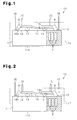
Fig. 1 is a front view illustrating a semiconductor device according to one embodiment of the present invention; -
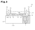
Fig. 2 is a front view illustrating a semiconductor device according to another embodiment; and -
Fig. 3 is a front view illustrating a semiconductor device according to another embodiment. - Hereinafter, a semiconductor device according to one embodiment of the present invention will be described with reference to
Fig. 1 . - As shown in
Fig. 1 , asemiconductor device 10 of the present embodiment includes aheat dissipation device 11, which serves as a cooling portion. Theheat dissipation device 11 includes abase body 11A made of ceramic, and a plurality of coolant channels T, which are formed in thebase body 11A. Coolant flows through the coolant channels T into thebase body 11A. Each ofmetal circuit boards 14, which serves as a circuit board, is joined to a mounting surface (surface for mounting an object to be cooled) 12 of theheat dissipation device 11. Each ofsemiconductor elements 13, which serves as an electronic part, is mounted on a corresponding one ofelement mounting surfaces 14a of themetal circuit boards 14. That is, eachmetal circuit board 14 is directly located between theheat dissipation device 11 and thecorresponding semiconductor element 13. Themetal circuit boards 14 serve as wiring layers (electrodes) and joining layers, and are made of pure aluminum (for example, 1000 series aluminum as aluminum for industrial use) or copper. As thesemiconductor elements 13, insulated gate bipolar transistors (IGBT) and diodes are used, for example. Soldering is used for joining themetal circuit boards 14 with thesemiconductor elements 13. Brazing is used for joining themetal circuit boards 14 with theheat dissipation device 11. A supply tube for supplying a coolant into theheat dissipation device 11, and a discharge tube for discharging the coolant, which has flowed through theheat dissipation device 11, outward are also connected to theheat dissipation device 11. The supply tube and the discharge tube are not illustrated. - In the
semiconductor device 10, each of metalconductive boards 15 used as an external connection terminal is joined to a terminal of the corresponding one of thesemiconductor elements 13. In thesemiconductor device 10, each ofmetal connecting pins 16 used as an external connection terminal is joined to themounting surface 12 of theheat dissipation device 11. Thesemiconductor elements 13 and the connectingpins 16 are electrically connected to each other through wires W, or wiring materials. Theconductive boards 15 and the connectingpins 16 are made of copper. Soldering or brazing is used for the joints between thesemiconductor elements 13 and theconductive boards 15 and the joints between theheat dissipation device 11 and the connectingpins 16. - For example, aluminum oxide, silicon nitride, silicon carbide, aluminum nitride, and alumina zirconium are used as a ceramic material that forms the
heat dissipation device 11. When employing a water cooled system as a cooling system of theheat dissipation device 11, it is preferable that the ceramic material have high water resistance. When the ceramic material is considered from a viewpoint of the stress relaxation by generation of heat of thesemiconductor elements 13, it is preferable that the ceramic material have a linear expansion coefficient that is closer to the linear expansion coefficient of thesemiconductor elements 13. Accordingly, eachmetal circuit board 14 is directly located between theheat dissipation device 11 and thecorresponding semiconductor element 13 with the liner expansion coefficients closer to each other. That is, eachmetal circuit board 14 directly contacts theheat dissipation device 11 and thecorresponding semiconductor element 13. The linear expansion coefficients of theheat dissipation device 11 and thesemiconductor elements 13 are less than the linear expansion coefficient of themetal circuit boards 14. - The
semiconductor device 10 according to the present embodiment is covered withresin 17, that is, molded in theresin 17, to cover the entireheat dissipation device 11 and various types of parts mounted on themounting surface 12 of theheat dissipation device 11. The entireheat dissipation device 11 refers to an entire surface including a surface (bottom surface) opposite to themounting surface 12 and lateral sides as well as themounting surface 12. Theentire semiconductor elements 13 and the entiremetal circuit boards 14 in the various types of the parts mounted on themounting surface 12 are covered with theresin 17. That is, theelement mounting surfaces 14a of themetal circuit boards 14, on which thesemiconductor element 13 are mounted, are also covered with theresin 17. Parts to be connected to peripheral portions in the various types of the parts mounted on themounting surface 12 are partially covered with theresin 17. Remaining portions of the parts are exposed outside of theresin 17. The parts to be connected to the peripheral portions include theconductive boards 15, the connectingpins 16, and the above supply tube and the discharge tube. Theresin 17 for molding is made of epoxy resin. The molding by theresin 17 is performed after the various types of the parts such as thesemiconductor elements 13, themetal circuit boards 14, theconductive boards 15, and the connectingpins 16 are joined and thesemiconductor elements 13 and the connectingpins 16 are bonded by the wires W. The molding by theresin 17 is performed at a temperature lower than the temperature at which the soldering of thesemiconductor elements 13 and themetal circuit boards 14 or the brazing of theheat dissipation device 11 and themetal circuit boards 14 is performed. - Hereinafter, an operation of the
semiconductor device 10 of the present embodiment will be described. - The coolant supplied from the coolant supply source flows through the supply tube connected to the
heat dissipation device 11 into each coolant channel T. The coolant, which has flowed into the coolant channels T, flows in the same direction. When the coolant flows through the coolant channels T as described above, the heat of thesemiconductor elements 13 transmitted through themetal circuit boards 14 to theheat dissipation device 11 is emitted through the coolant, which flows through the coolant channels T. The coolant after the heat exchange, which has flowed through the coolant channels T, is discharged outside through the discharge tube connected to theheat dissipation device 11. Since theheat dissipation device 11 of the present embodiment is made of ceramic, theheat dissipation device 11 has an insulating function as well as the cooling function. - Accordingly, the present embodiment has the following advantages.
- (1) The
semiconductor device 10 of the present embodiment employs theheat dissipation device 11 made of ceramic, which is formed by integrating the insulating portion and the coolant channels. Thesemiconductor device 10, which includes theheat dissipation device 11, is covered with theresin 17, that is, molded in theresin 17. Theheat dissipation device 11 made of ceramic itself has both the insulating function and the cooling function. This simplifies the configuration of thesemiconductor device 10 more than in the case where a DBA board (substrate formed by joining metal boards to both of the front and back sides of the insulating substrate made of ceramic) is joined to a metal heat dissipation device as in the conventional case. That is, in thesemiconductor device 10 of the present embodiment, themetal circuit boards 14, on which thesemiconductor elements 13 are mounted, are directly joined to theheat dissipation device 11. This simplifies the configuration of thesemiconductor device 10. - (2) The
heat dissipation device 11 made of ceramic is employed. Accordingly, thesemiconductor device 10 inherently includes a structure in which heat stress is not easily generated. Thesemiconductor device 10 is molded in theresin 17. This improves the reliability of the joined portions between thesemiconductor elements 13 and themetal circuit boards 14 and the joined portions between themetal circuit boards 14 and theheat dissipation device 11. That is, a thermal deformation is limited according to the moldedresin 17. This improves the reliability of each joined portion. According to thesemiconductor device 10 of the present embodiment, the stress relaxation member, which is located between the circuit board and the heat dissipation device in the conventional semiconductor device, is omitted by employing theheat dissipation device 11 made of ceramic. - (3) Each
metal circuit board 14 is directly located between theheat dissipation device 11 made of ceramic and thecorresponding semiconductor element 13, which has a linear expansion coefficient less than the linear expansion coefficient of themetal circuit board 14. This limits the generation of the thermal stress. Accordingly, the reliability of each joined portion is further improved. - (4) The
entire semiconductor elements 13 and the entiremetal circuit boards 14 are covered with theresin 17. This eliminates the necessity for a structure for fixing these parts to theheat dissipation device 11, for example, a fixation structure for pressing and holding thesemiconductor elements 13 and themetal circuit boards 14 toward theheat dissipation device 11. This further simplifies the configuration of thesemiconductor device 10. - (5) The entire
heat dissipation device 11 is covered with theresin 17 as well as thesemiconductor elements 13 and themetal circuit boards 14. This facilitates the handling of thesemiconductor device 10. When theheat dissipation device 11 is made of ceramic, theheat dissipation device 11 is inferior in strength to the metalheat dissipation device 11. However, since the protection performance of theheat dissipation device 11 is improved by covering the entireheat dissipation device 11 with theresin 17, the handling of thesemiconductor device 10 is facilitated, and the long-term excellent heat dissipation performance is achieved. In particular, in the attachment process such as the case of mounting thesemiconductor device 10 on a vehicle, the handling is facilitated to improve the operability. This is advantageous. - (6) The entire
heat dissipation device 11 is covered with theresin 17. This improves the sealing property of theheat dissipation device 11. This improves the heat dissipation performance. - (7) The
semiconductor device 10 is molded in theresin 17 so that the reliability of each joined portion is improved. This maintains the performance (reliability) of thesemiconductor device 10 over an extended period of time. That is, the degradation of thesemiconductor device 10 is limited. - (8) Since the difference in the linear expansion coefficients of the
resin 17 and the ceramic is small, the desired reliability of the joined portion between theresin 17 and theheat dissipation device 11 made of ceramic is also obtained. That is, theresin 17 is not easily separated from theheat dissipation device 11 at the joined portion. This maintains the above advantages (2), (4), and (5) to (7), which can be generated by the moldedresin 17, over an extended period of time. - (9) The
heat dissipation device 11 made of ceramic is employed. This reduces the size of thesemiconductor device 10 as well as simplifying the configuration of thesemiconductor device 10. Accordingly, when mounting thesemiconductor device 10 on a vehicle, the space occupied by thesemiconductor device 10 is reduced. This expands the flexibility of design. - The present embodiment may be modified as follows.
- As shown in
Fig. 2 , the region to be molded in theresin 17 may be reduced to a part of the lateral sides of theheat dissipation device 11 in place of the configuration in which the entireheat dissipation device 11 is covered with theresin 17. That is, the surface opposite to the mountingsurface 12 of theheat dissipation device 11 is exposed without being covered with theresin 17. The entire mountingsurface 12 and a part of the lateral sides of theheat dissipation device 11 are molded with theresin 17. This allows a heating body to be cooled on the opposite surface as well. The amount of theresin 17 is reduced. This contributes to the reduction of the manufacturing cost of thesemiconductor device 10. The amount of theresin 17 is reduced. This relaxes the stress received from the moldedresin 17. - As shown in
Fig. 3 , the region to be molded in theresin 17 may be reduced to only the mountingsurface 12 of theheat dissipation device 11 in place of the configuration in which the entireheat dissipation device 11 is covered with theresin 17. Only the mountingsurface 12 of theheat dissipation device 11 is molded in theresin 17. That is, the entire surface opposite to the mountingsurface 12 of theheat dissipation device 11 is exposed without being covered with theresin 17. The entire lateral sides of theheat dissipation device 11 are also exposed. According to this, the same advantage as that of another embodiment described above with reference toFig. 2 is obtained, and the amount of theresin 17 is further reduced. - In the embodiments described with reference to
Figs. 2 and3 , when joining the heating body to the opposite surface of theheat dissipation device 11, the entireheat dissipation device 11 including the heating body may be molded in theresin 17. - The
heat dissipation device 11 may be made of resin in place of ceramic. - The configurations of the various types of the parts to be mounted on the
heat dissipation device 11 may be changed. - The coolant channel T in the
heat dissipation device 11 may be a linear channel as viewed from above, or a wavy channel or a zigzag channel as viewed from above. In the wavy or zigzag channel, the flow of the coolant is more turbulent than the flow in the linear channel. This improves the cooling performance according to the effect of the turbulent flow. - The coolant, which flows through the
heat dissipation device 11, may be a liquid coolant or a gas coolant.
Claims (7)
- A semiconductor device, comprising:a cooling portion, which is made of ceramic or resin and includes a mounting surface;a metal circuit board, which is mounted on the mounting surface of the cooling portion and includes an element mounting surface; anda semiconductor element mounted on the element mounting surface of the circuit board, wherein at least a part of the circuit board that corresponds to the element mounting surface is covered with resin with respect to the cooling portion.
- The semiconductor device according to claim 1, wherein the cooling portion is made of ceramic.
- The semiconductor device according to claim 2, wherein a linear expansion coefficient of each of the semiconductor element and the cooling portion is less than a linear expansion coefficient of the circuit board, and the circuit board is directly located between the semiconductor element and the cooling portion.
- The semiconductor device according to any one of claims 1 to 3, wherein the semiconductor element, the circuit board, and the cooling portion are covered with the resin.
- The semiconductor device according to any one of claims 1 to 3, wherein
the entire semiconductor element and the entire circuit board are covered with the resin,
the cooling portion includes an opposite surface, which is positioned opposite to the mounting surface, and
the cooling portion is covered with the resin such that at least the entire opposite surface is exposed. - The semiconductor device according to claim 5, wherein
the cooling portion includes a lateral side, and
the entire mounting surface of the cooling portion and a part of the lateral side are covered with the resin. - The semiconductor device according to claim 5, wherein
the cooling portion includes a lateral side, and
the mounting surface of the cooling portion is covered with the resin such that the entire lateral side of the cooling portion and the entire opposite surface are exposed.
Applications Claiming Priority (2)
| Application Number | Priority Date | Filing Date | Title |
|---|---|---|---|
| JP2011271575A JP2013123014A (en) | 2011-12-12 | 2011-12-12 | Semiconductor device |
| PCT/JP2012/078895 WO2013088864A1 (en) | 2011-12-12 | 2012-11-07 | Semiconductor device |
Publications (2)
| Publication Number | Publication Date |
|---|---|
| EP2793260A1 true EP2793260A1 (en) | 2014-10-22 |
| EP2793260A4 EP2793260A4 (en) | 2015-08-12 |
Family
ID=48612319
Family Applications (1)
| Application Number | Title | Priority Date | Filing Date |
|---|---|---|---|
| EP12857172.6A Withdrawn EP2793260A4 (en) | 2011-12-12 | 2012-11-07 | SEMICONDUCTOR DEVICE |
Country Status (6)
| Country | Link |
|---|---|
| US (1) | US20140332950A1 (en) |
| EP (1) | EP2793260A4 (en) |
| JP (1) | JP2013123014A (en) |
| KR (1) | KR20140088181A (en) |
| CN (1) | CN103988298A (en) |
| WO (1) | WO2013088864A1 (en) |
Cited By (2)
| Publication number | Priority date | Publication date | Assignee | Title |
|---|---|---|---|---|
| WO2015135010A1 (en) * | 2014-03-10 | 2015-09-17 | Egston System Electronics Eggenburg Gmbh | Electric component assembly |
| EP3038152A1 (en) * | 2014-12-26 | 2016-06-29 | Kabushiki Kaisha Toshiba | Wiring board and semiconductor package including wiring board |
Families Citing this family (10)
| Publication number | Priority date | Publication date | Assignee | Title |
|---|---|---|---|---|
| JP6524709B2 (en) * | 2014-06-13 | 2019-06-05 | 日産自動車株式会社 | Semiconductor device |
| KR102421016B1 (en) * | 2014-09-09 | 2022-07-13 | 세람테크 게엠베하 | Multi-layer cooling element |
| DE102015106552B4 (en) * | 2015-04-28 | 2022-06-30 | Infineon Technologies Ag | Electronic module with fluid cooling channel and method for manufacturing the same |
| DE102015107489B4 (en) * | 2015-05-12 | 2020-07-02 | Infineon Technologies Ag | Method for reducing sheet resistance in an electronic device |
| WO2017159505A1 (en) * | 2016-03-18 | 2017-09-21 | 富士電機株式会社 | Semiconductor device, metal electrode member and semiconductor device production method |
| KR102152668B1 (en) * | 2016-04-15 | 2020-09-07 | 교세라 가부시키가이샤 | Semiconductor device |
| DE102016114303A1 (en) | 2016-08-02 | 2018-02-08 | Infineon Technologies Ag | Pack with partially enclosed cooling channel for cooling an encapsulated chip |
| JP6885175B2 (en) * | 2017-04-14 | 2021-06-09 | 富士電機株式会社 | Semiconductor device |
| US20190357386A1 (en) * | 2018-05-16 | 2019-11-21 | GM Global Technology Operations LLC | Vascular polymeric assembly |
| CN113078135A (en) * | 2020-01-06 | 2021-07-06 | 珠海零边界集成电路有限公司 | Chip packaging structure |
Family Cites Families (17)
| Publication number | Priority date | Publication date | Assignee | Title |
|---|---|---|---|---|
| EP0484180A1 (en) * | 1990-11-01 | 1992-05-06 | Fujitsu Limited | Packaged semiconductor device having an optimized heat dissipation |
| US5430331A (en) * | 1993-06-23 | 1995-07-04 | Vlsi Technology, Inc. | Plastic encapsulated integrated circuit package having an embedded thermal dissipator |
| JP2795626B2 (en) * | 1995-08-21 | 1998-09-10 | 北川工業株式会社 | Electronic components with heat dissipation function |
| JP2002026469A (en) * | 2000-07-11 | 2002-01-25 | Denki Kagaku Kogyo Kk | Circuit board with direct cooling structure |
| TW511422B (en) * | 2000-10-02 | 2002-11-21 | Sanyo Electric Co | Method for manufacturing circuit device |
| JP2002329938A (en) * | 2001-04-27 | 2002-11-15 | Kyocera Corp | Ceramic circuit board |
| JP4228830B2 (en) * | 2003-08-06 | 2009-02-25 | 株式会社デンソー | Semiconductor cooling unit |
| JP4207710B2 (en) * | 2003-08-08 | 2009-01-14 | 株式会社デンソー | Semiconductor device |
| JP4028452B2 (en) * | 2003-08-27 | 2007-12-26 | Dowaホールディングス株式会社 | Electronic component mounting substrate and manufacturing method thereof |
| JP2007184479A (en) * | 2006-01-10 | 2007-07-19 | Toyota Central Res & Dev Lab Inc | A cooler and a semiconductor device in which a semiconductor element is mounted on the cooler |
| JP4821537B2 (en) * | 2006-09-26 | 2011-11-24 | 株式会社デンソー | Electronic control unit |
| JP4826426B2 (en) * | 2006-10-20 | 2011-11-30 | 株式会社デンソー | Semiconductor device |
| JP5713578B2 (en) * | 2010-04-06 | 2015-05-07 | 株式会社アテクト | Substrate manufacturing method |
| EP2565920A4 (en) * | 2010-04-28 | 2016-12-21 | Toyota Jidoshokki Kk | HEAT DISSIPATING DEVICE AND SEMICONDUCTOR DEVICE |
| JP2011238643A (en) * | 2010-05-06 | 2011-11-24 | Denso Corp | Power semiconductor module |
| JP5593864B2 (en) * | 2010-06-10 | 2014-09-24 | トヨタ自動車株式会社 | Semiconductor device cooler |
| JP5511621B2 (en) * | 2010-10-13 | 2014-06-04 | 三菱電機株式会社 | Semiconductor device |
-
2011
- 2011-12-12 JP JP2011271575A patent/JP2013123014A/en active Pending
-
2012
- 2012-11-07 CN CN201280060687.7A patent/CN103988298A/en active Pending
- 2012-11-07 WO PCT/JP2012/078895 patent/WO2013088864A1/en not_active Ceased
- 2012-11-07 US US14/363,189 patent/US20140332950A1/en not_active Abandoned
- 2012-11-07 KR KR1020147014321A patent/KR20140088181A/en not_active Ceased
- 2012-11-07 EP EP12857172.6A patent/EP2793260A4/en not_active Withdrawn
Cited By (2)
| Publication number | Priority date | Publication date | Assignee | Title |
|---|---|---|---|---|
| WO2015135010A1 (en) * | 2014-03-10 | 2015-09-17 | Egston System Electronics Eggenburg Gmbh | Electric component assembly |
| EP3038152A1 (en) * | 2014-12-26 | 2016-06-29 | Kabushiki Kaisha Toshiba | Wiring board and semiconductor package including wiring board |
Also Published As
| Publication number | Publication date |
|---|---|
| KR20140088181A (en) | 2014-07-09 |
| JP2013123014A (en) | 2013-06-20 |
| WO2013088864A1 (en) | 2013-06-20 |
| US20140332950A1 (en) | 2014-11-13 |
| CN103988298A (en) | 2014-08-13 |
| EP2793260A4 (en) | 2015-08-12 |
Similar Documents
| Publication | Publication Date | Title |
|---|---|---|
| US20140332950A1 (en) | Semiconductor device | |
| US10128166B2 (en) | Power semiconductor module | |
| CN102315184B (en) | Semiconductor device | |
| US9379083B2 (en) | Semiconductor device and method for manufacturing semiconductor device | |
| EP3771084A1 (en) | Double-sided cooling type power module and manufacturing method therefor | |
| JP6315091B2 (en) | Cooler and fixing method of cooler | |
| CN112683411B (en) | semiconductor modules | |
| US11538736B2 (en) | Cooling apparatus, semiconductor module, and vehicle | |
| EP1843392A1 (en) | Electronics assembly having heat sink substrate disposed in cooling vessel | |
| US10163752B2 (en) | Semiconductor device | |
| CN102683301B (en) | Semiconductor devices including base | |
| JP7367394B2 (en) | Semiconductor module, vehicle and manufacturing method | |
| CN105264658A (en) | Semiconductor module | |
| JP3646665B2 (en) | Inverter device | |
| JP4826426B2 (en) | Semiconductor device | |
| US20210005528A1 (en) | Semiconductor module, semiconductor device, and manufacturing method of semiconductor module | |
| US20100102431A1 (en) | Power module and inverter for vehicles | |
| JP4935783B2 (en) | Semiconductor device and composite semiconductor device | |
| JP2004235175A (en) | Power semiconductor module | |
| JP2009283766A (en) | Semiconductor device | |
| US12635515B2 (en) | Semiconductor power device, semiconductor power system and method for cooling a semiconductor power device | |
| EP4266365A1 (en) | Semiconductor power device, semiconductor power system and method for cooling a semiconductor power device | |
| WO2025225203A1 (en) | Semiconductor module and semiconductor device | |
| CN115206904A (en) | Semiconductor module and semiconductor device | |
| JP2018129487A (en) | Semiconductor device |
Legal Events
| Date | Code | Title | Description |
|---|---|---|---|
| PUAI | Public reference made under article 153(3) epc to a published international application that has entered the european phase |
Free format text: ORIGINAL CODE: 0009012 |
|
| 17P | Request for examination filed |
Effective date: 20140603 |
|
| AK | Designated contracting states |
Kind code of ref document: A1 Designated state(s): AL AT BE BG CH CY CZ DE DK EE ES FI FR GB GR HR HU IE IS IT LI LT LU LV MC MK MT NL NO PL PT RO RS SE SI SK SM TR |
|
| DAX | Request for extension of the european patent (deleted) | ||
| RA4 | Supplementary search report drawn up and despatched (corrected) |
Effective date: 20150710 |
|
| RIC1 | Information provided on ipc code assigned before grant |
Ipc: H01L 25/07 20060101ALI20150706BHEP Ipc: H01L 23/473 20060101AFI20150706BHEP |
|
| 17Q | First examination report despatched |
Effective date: 20150730 |
|
| STAA | Information on the status of an ep patent application or granted ep patent |
Free format text: STATUS: THE APPLICATION IS DEEMED TO BE WITHDRAWN |
|
| 18D | Application deemed to be withdrawn |
Effective date: 20151210 |