EP2793252A1 - Method for manufacturing semiconductor device - Google Patents
Method for manufacturing semiconductor device Download PDFInfo
- Publication number
- EP2793252A1 EP2793252A1 EP12857979.4A EP12857979A EP2793252A1 EP 2793252 A1 EP2793252 A1 EP 2793252A1 EP 12857979 A EP12857979 A EP 12857979A EP 2793252 A1 EP2793252 A1 EP 2793252A1
- Authority
- EP
- European Patent Office
- Prior art keywords
- forming
- metal film
- insulating film
- contact
- semiconductor device
- Prior art date
- Legal status (The legal status is an assumption and is not a legal conclusion. Google has not performed a legal analysis and makes no representation as to the accuracy of the status listed.)
- Withdrawn
Links
Images



Classifications
-
- H—ELECTRICITY
- H10—SEMICONDUCTOR DEVICES; ELECTRIC SOLID-STATE DEVICES NOT OTHERWISE PROVIDED FOR
- H10D—INORGANIC ELECTRIC SEMICONDUCTOR DEVICES
- H10D12/00—Bipolar devices controlled by the field effect, e.g. insulated-gate bipolar transistors [IGBT]
- H10D12/01—Manufacture or treatment
- H10D12/031—Manufacture or treatment of IGBTs
-
- H—ELECTRICITY
- H10—SEMICONDUCTOR DEVICES; ELECTRIC SOLID-STATE DEVICES NOT OTHERWISE PROVIDED FOR
- H10D—INORGANIC ELECTRIC SEMICONDUCTOR DEVICES
- H10D12/00—Bipolar devices controlled by the field effect, e.g. insulated-gate bipolar transistors [IGBT]
- H10D12/01—Manufacture or treatment
- H10D12/031—Manufacture or treatment of IGBTs
- H10D12/032—Manufacture or treatment of IGBTs of vertical IGBTs
-
- H—ELECTRICITY
- H10—SEMICONDUCTOR DEVICES; ELECTRIC SOLID-STATE DEVICES NOT OTHERWISE PROVIDED FOR
- H10D—INORGANIC ELECTRIC SEMICONDUCTOR DEVICES
- H10D12/00—Bipolar devices controlled by the field effect, e.g. insulated-gate bipolar transistors [IGBT]
- H10D12/411—Insulated-gate bipolar transistors [IGBT]
- H10D12/441—Vertical IGBTs
-
- H—ELECTRICITY
- H10—SEMICONDUCTOR DEVICES; ELECTRIC SOLID-STATE DEVICES NOT OTHERWISE PROVIDED FOR
- H10D—INORGANIC ELECTRIC SEMICONDUCTOR DEVICES
- H10D30/00—Field-effect transistors [FET]
- H10D30/01—Manufacture or treatment
- H10D30/021—Manufacture or treatment of FETs having insulated gates [IGFET]
-
- H—ELECTRICITY
- H10—SEMICONDUCTOR DEVICES; ELECTRIC SOLID-STATE DEVICES NOT OTHERWISE PROVIDED FOR
- H10D—INORGANIC ELECTRIC SEMICONDUCTOR DEVICES
- H10D30/00—Field-effect transistors [FET]
- H10D30/01—Manufacture or treatment
- H10D30/021—Manufacture or treatment of FETs having insulated gates [IGFET]
- H10D30/028—Manufacture or treatment of FETs having insulated gates [IGFET] of double-diffused metal oxide semiconductor [DMOS] FETs
- H10D30/0291—Manufacture or treatment of FETs having insulated gates [IGFET] of double-diffused metal oxide semiconductor [DMOS] FETs of vertical DMOS [VDMOS] FETs
-
- H—ELECTRICITY
- H10—SEMICONDUCTOR DEVICES; ELECTRIC SOLID-STATE DEVICES NOT OTHERWISE PROVIDED FOR
- H10D—INORGANIC ELECTRIC SEMICONDUCTOR DEVICES
- H10D30/00—Field-effect transistors [FET]
- H10D30/60—Insulated-gate field-effect transistors [IGFET]
- H10D30/64—Double-diffused metal-oxide semiconductor [DMOS] FETs
- H10D30/66—Vertical DMOS [VDMOS] FETs
-
- H—ELECTRICITY
- H10—SEMICONDUCTOR DEVICES; ELECTRIC SOLID-STATE DEVICES NOT OTHERWISE PROVIDED FOR
- H10D—INORGANIC ELECTRIC SEMICONDUCTOR DEVICES
- H10D62/00—Semiconductor bodies, or regions thereof, of devices having potential barriers
- H10D62/80—Semiconductor bodies, or regions thereof, of devices having potential barriers characterised by the materials
- H10D62/83—Semiconductor bodies, or regions thereof, of devices having potential barriers characterised by the materials being Group IV materials, e.g. B-doped Si or undoped Ge
- H10D62/832—Semiconductor bodies, or regions thereof, of devices having potential barriers characterised by the materials being Group IV materials, e.g. B-doped Si or undoped Ge being Group IV materials comprising two or more elements, e.g. SiGe
- H10D62/8325—Silicon carbide
-
- H—ELECTRICITY
- H10—SEMICONDUCTOR DEVICES; ELECTRIC SOLID-STATE DEVICES NOT OTHERWISE PROVIDED FOR
- H10D—INORGANIC ELECTRIC SEMICONDUCTOR DEVICES
- H10D64/00—Electrodes of devices having potential barriers
- H10D64/01—Manufacture or treatment
- H10D64/011—Manufacture or treatment of electrodes ohmically coupled to a semiconductor
- H10D64/0111—Manufacture or treatment of electrodes ohmically coupled to a semiconductor to Group IV semiconductors
- H10D64/0115—Manufacture or treatment of electrodes ohmically coupled to a semiconductor to Group IV semiconductors to silicon carbide
-
- H—ELECTRICITY
- H10—SEMICONDUCTOR DEVICES; ELECTRIC SOLID-STATE DEVICES NOT OTHERWISE PROVIDED FOR
- H10D—INORGANIC ELECTRIC SEMICONDUCTOR DEVICES
- H10D64/00—Electrodes of devices having potential barriers
- H10D64/60—Electrodes characterised by their materials
- H10D64/62—Electrodes ohmically coupled to a semiconductor
Definitions
- the present invention relates to a method for manufacturing a semiconductor device, more particularly, a method for manufacturing a semiconductor device, by which a semiconductor device having a stable characteristic can be manufactured by improving adhesion between an electrode containing aluminum and an interlayer insulating film.
- An electrode containing aluminum (A1) may be employed for a source electrode of a MOSFET (Metal Oxide Semiconductor Field Effect Transistor) or an emitter electrode of an IGBT (Insulated Gate Bipolar Transistor).
- MOSFET Metal Oxide Semiconductor Field Effect Transistor
- IGBT Insulated Gate Bipolar Transistor
- a positional relation or the like between such a source electrode containing Al and each of a gate electrode, a gate insulating film, and an interlayer insulating film has been considered (for example, see United States Patent No. 6,833,562 (Patent Literature 1) and Japanese Patent Laying-Open No. 2000-012846 (Patent Literature 2)).
- the source electrode may be formed on and in contact with a surface of a substrate having an active region formed therein, and in contact with a side wall surface of an interlayer insulating film formed to surround the gate electrode on the surface.
- adhesion between the source electrode and the interlayer insulating film is insufficient, the source electrode comes off, thus affecting a device characteristic of the MOSFET.
- the present invention has been made in view of the foregoing problem, and has its object to provide a method for manufacturing a semiconductor device, by which a semiconductor device having a stable characteristic can be manufactured by improving adhesion between an electrode containing aluminum and an interlayer insulating film.
- a method for manufacturing a semiconductor device in the present invention includes the steps of: preparing a substrate made of silicon carbide; forming a gate insulating film on a surface of the substrate; forming a gate electrode on the gate insulating film; forming an interlayer insulating film on the gate insulating film so as to surround the gate electrode; forming a contact hole extending through the interlayer insulating film to expose the surface of the substrate and separated from the gate electrode; forming a first metal film on and in contact with a side wall surface of the contact hole, the first metal film containing at least one of Ti and Si and containing no Al; forming a second metal film containing Ti, Al, and Si on and in contact with the first metal film; and forming a source electrode containing Ti, Al, and Si by heating the first and second metal films.
- first metal film containing no Al is intended to indicate a first metal film containing substantially no Al.
- first metal film is intended to indicate a metal film in which Al is not added intentionally, and include a first metal film in which Al is contained as an impurity, for example.
- the source electrode containing Al is formed in the following manner. First, the contact hole is formed to extend through the interlayer insulating film surrounding the gate electrode, and the first metal film containing at least one of Ti and Si is formed on and in contact with the side wall surface of the contact hole. Next, the second metal film containing Ti, Al, and Si is formed on and in contact with the first metal film. Then, by heating the first and second metal films, the source electrode containing Ti, Al, and Si is formed.
- adhesion between the source electrode and the interlayer insulating film can be improved by forming the first metal film, which contains at least one of Ti and Si, in advance on and in contact with the side wall surface of the contact hole.
- the method for manufacturing the semiconductor device in the present invention there can be provided a method for manufacturing a semiconductor device, by which a semiconductor device having a stable characteristic can be manufactured by improving adhesion between the source electrode, which is an electrode containing aluminum, and the interlayer insulating film.
- the second metal film in the step of forming the second metal film, may be formed in contact with the surface of the substrate exposed by forming the contact hole.
- the second metal film in the step of forming the second metal film, may be formed to have a first metal layer, a second metal layer, and a third metal layer stacked on one another, the first metal layer containing Ti, the second metal layer being on and in contact with the first metal layer and containing Al, the third metal layer being on and in contact with the second metal layer and containing Si.
- the second metal film in the step of forming the second metal film, may be formed to contain Ti, Al, and Si mixed with one another. In this way, the second metal film can be formed readily.
- the first metal film in the step of forming the first metal film, may be formed to have a thickness of not less than 0.1 ⁇ m and not more than 1 ⁇ m.
- the thickness of the first metal film can be set in a range necessary to improve adhesion between the source electrode and the interlayer insulating film.
- the first metal film in the step of forming the first metal film, may be formed to contain Ti and contain no Al. In this way, the adhesion between the source electrode and the interlayer insulating film can be further improved.
- a method for manufacturing a semiconductor device by which a semiconductor device having a stable characteristic can be manufactured by improving adhesion between an electrode containing aluminum and an interlayer insulating film.
- MOSFET 1 includes a substrate 10 made of silicon carbide, gate insulating films 20, gate electrodes 30, interlayer insulating films 40, source electrodes 50, a source wire 60, and a drain electrode 70.
- Substrate 10 includes a base substrate 11 and a semiconductor layer 12.
- semiconductor layer 12 a drift region 13, body regions 14, source regions 15, and contact regions 16 are formed.
- contact holes 80 are formed to extend through gate insulating film 20 and interlayer insulating film 40 and expose a main surface 10A of substrate 10.
- Base substrate 11 contains an n type impurity such as N (nitrogen) and therefore has n type conductivity (first conductivity type).
- Drift region 13 is an epitaxial growth layer formed on a main surface 11A of base substrate 11. As with base substrate 11, drift region 13 contains an n type impurity such as N (nitrogen), and therefore has n type conductivity. The concentration thereof in drift region 13 is lower than that in base substrate 11.
- Body regions 14 include main surface 10A of substrate 10, and are formed to be separated from each other in semiconductor layer 12.
- Each of body regions 14 contains a p type impurity such as Al (aluminum) or B (boron), and therefore has p type conductivity (second conductivity type).
- Source regions 15 include main surface 10A, and are formed in body regions 14 such that they are surrounded by body regions 14.
- Each of source regions 15 contains an n type impurity such as P (phosphorus), and therefore has n type conductivity as with base substrate 11 and drift region 13. Further, the concentration of the n type impurity in source region 15 is higher than the concentration of the n type impurity in drift region 13.
- contact regions 16 include main surface 10A, are surrounded by body regions 14, and are respectively formed in body regions 14 so as to be adjacent to source regions 15.
- each of contact regions 16 contains a p type impurity such as Al (aluminum) or B (boron) and therefore has p type conductivity. The concentration thereof in contact region 16 is higher than that in body region 14.
- Each of gate insulating films 20 is made of, for example, SiO 2 (silicon dioxide), is formed to be disposed on and in contact with main surface 10A and extend from the upper surface of one source region 15 to the upper surface of the other source region 15.
- Each of gate electrodes 30 is disposed on and in contact with gate insulating film 20, and is formed to extend from one source region 15 to the other source region 15.
- Gate electrode 30 is made of a conductor such as polysilicon having an impurity added therein, for example.
- Interlayer insulating film 40 is made of for example, SiO 2 (silicon dioxide), and is formed on gate insulating film 20 to surround gate electrode 30.
- Each of contact holes 80 has side wall surfaces 80A and a bottom surface 80B, and is formed to extend through interlayer insulating film 40 and gate insulating film 20. Further, as shown in Fig. 1 , each of side wall surfaces 80A of contact hole 80 is constituted of interlayer insulating film 40 and gate insulating film 20, and bottom surface 80B thereof corresponds to the upper surfaces of source region 15 and contact region 16.
- source electrode 50 is formed on and in contact with side wall surface 80A and bottom surface 80B. Further, source electrode 50 is made of an alloy containing Ti, Al, and Si, such as a TiAlSi alloy, and is electrically connected to source region 15.
- Drain electrode 70 is formed on a main surface 11B of base substrate 11 opposite to main surface 11 A thereof. As with source electrode 50, drain electrode 70 is made of, for example, a TiAlSi alloy, and is electrically connected to base substrate 11.
- Source wire 60 is formed to cover source electrode 50 and interlayer insulating film 40.
- Source wire 60 is made of a metal such as Al (aluminum), and is electrically connected to source region 15 via source electrode 50.
- MOSFET 1 serving as the semiconductor device according to the present embodiment.
- a voltage is applied between source electrode 50 and drain electrode 70 while an applied voltage to gate electrode 30 is smaller than a threshold voltage, i.e., while it is in OFF state, a pn junction formed between body region 14 and drift region 13 is reverse-biased. Accordingly, MOSFET 1 is in the non-conductive state.
- gate electrode 30 is fed with a voltage equal to or greater than the threshold voltage, an inversion layer is formed in body region 14.
- source region 15 and drift region 13 are electrically connected to each other, whereby a current flows between source electrode 50 and drain electrode 70. In the manner described above, MOSFET 1 operates.
- MOSFET 1 serving as the semiconductor device according to the present embodiment is manufactured.
- a substrate preparing step (S10) is first performed.
- steps (S11) to (S 14) described below are performed to prepare substrate 10 made of silicon carbide.
- step (S 11) a base substrate preparing step is performed.
- this step (S11) referring to Fig. 3 , an ingot (not shown) made of, for example, 4H-SiC is sliced to prepare base substrate 11 having n type conductivity.
- step (S12) an epitaxial growth layer forming step is performed.
- semiconductor layer 12 having n type conductivity is formed by epitaxial growth on main surface 11 A of base substrate 11.
- step (S 13) an ion implantation step is performed.
- Al ions are first implanted into regions including main surface 10A of substrate 10, thereby forming body regions 14 of p type conductivity in semiconductor layer 12.
- P ions are implanted into each of body regions 14 at a depth shallower than the depth in which the Al ions have been implanted, thereby forming source region 15 of n type conductivity.
- Al ions are further implanted into body region 14, thereby forming contact region 16 adjacent to source region 15, having the same depth as that of source region 15, and having p type conductivity.
- a region in which none of body region 14, source region 15, and contact region 16 is formed serves as drift region 13.
- step (S 14) an activation annealing step is performed.
- this step (S14) by heating substrate 10, the impurities implanted in step (S13) are activated. Accordingly, desired carriers are generated in the regions having the impurities implanted therein.
- substrate 10 is prepared in which an active region is formed by the implantation of the impurities.
- a gate insulating film forming step is performed.
- this step (S20) referring to Fig. 5 , for example, by heating substrate 10 in an atmosphere containing oxygen, gate insulating film 20 made of SiO 2 (silicon dioxide) is formed to cover main surface 10A of substrate 10.
- SiO 2 silicon dioxide
- a gate electrode forming step is performed.
- this step (S30) referring to Fig. 6 , for example, an LPCVD (Low Pressure Chemical Vapor Deposition) method is employed to form gate electrode 30, which is made of polysilicon containing an impurity, on gate insulating film 20.
- LPCVD Low Pressure Chemical Vapor Deposition
- an interlayer insulating film forming step is performed.
- a P (Plasma)-CVD method is employed to form interlayer insulating film 40 made of SiO 2 (silicon dioxide) on gate insulating film 20 such that interlayer insulating film 40 and gate insulating film 20 surround gate electrode 30.
- a contact hole forming step is performed.
- contact hole 80 is formed to have side wall surface 80A and bottom surface 80B and expose main surface 10A of substrate 10.
- an etching method such as RIE (Reactive Ion Etching) is employed to etch through interlayer insulating film 40 and gate insulating film 20, thereby forming contact hole 80 exposing main surface 10A of substrate 10 (the upper surfaces of source region 15 and contact region 16).
- contact hole 80 is formed to be separated from gate electrode 30.
- gate electrode 30 is maintained to be surrounded by gate insulating film 20 and interlayer insulating film 40.
- a first metal film forming step is performed.
- sputtering is performed to form a first metal film 51 on side wall surface 80A and bottom surface 80B of contact hole 80 and the upper surface of interlayer insulating film 40.
- first metal film 51 containing at least one of Ti and Si and containing no Al such as first metal film 51 made of Ti or Si, first metal film 51 formed of a mixed film of Ti and Si, or a first metal film 51 formed of a stacked film of Ti and Si.
- step (S70) an etching step is performed.
- this step (S70) as indicated by arrows in Fig. 10 , dry etching is performed from the side of main surface 10A of substrate 10, thereby removing first metal film 51 from the upper surface of interlayer insulating film 40 and bottom surface 80B of contact hole 80 while first metal film 51 remains on side wall surface 80A of contact hole 80.
- a second metal film forming step is performed.
- a second metal film 52 containing Ti, Al, and Si is formed on and in contact with first metal film 51.
- sputtering is performed to form second metal film 52 structured to include a first metal layer 52a, a second metal layer 52b, and a third metal layer 52c stacked on one another.
- First metal layer 52a contains Ti.
- Second metal layer 52b is on and in contact with first metal layer 52a and contains Al.
- Third metal layer 52c is on and in contact with second metal layer 52b and contains Si.
- a second metal film 52 formed of a stacked film of first to third metal layers 52a, b, c may be formed, or a second metal film 52 in which Ti, Al, and Si are mixed by simultaneously sputtering Ti, Al, and Si may be formed.
- step (S90) an etching step is performed.
- this step (S90) as indicated by arrows in Fig. 13 , dry etching is performed from the side of main surface 10A of substrate 10, thereby mainly removing second metal film 52 from the upper surface of interlayer insulating film 40 while second metal film 52 on and in contact with first metal film 51 and bottom surface 80B of contact hole 80 remains.
- a third metal film forming step is performed.
- a third metal film 71 made of, for example, Ti, Al, and Si is formed on main surface 11B of base substrate 11.
- step (S110) an alloying annealing step is performed.
- step (S100) referring to Fig. 1 , first and second metal films 51, 52 formed in steps (S60) and (S80) as well as third metal film 71 formed in step (S100) are heated. Accordingly, Ti, Al, and Si are alloyed, thereby forming source electrodes 50 and drain electrode 70 each made of a TiAlSi alloy.
- a wire forming step is performed.
- a deposition method is employed to form source wire 60, which is made of a conductor such as Al, on and in contact with source electrode 50.
- MOSFET 1 is manufactured, thus completing the method for manufacturing the semiconductor device in the present embodiment.
- source electrode 50 containing Al is formed in the following manner. First, contact hole 80 is formed to extend through interlayer insulating film 40 surrounding gate electrode 30, and first metal film 51 containing at least one of Ti and Si is formed on and in contact with side wall surface 80A of contact hole 80. Next, second metal film 52 containing Ti, Al, and Si is formed on and in contact with first metal film 51. Then, by heating first and second metal films 51, 52, source electrode 50 containing Ti, Al, and Si is formed.
- adhesion between source electrode 50 and interlayer insulating film 40 can be improved by forming first metal film 51, which contains at least one of Ti and Si, in advance on and in contact with side wall surface 80A of contact hole 80.
- MOSFET 1 having a stable characteristic can be manufactured by improving adhesion between source electrode 50 containing aluminum and interlayer insulating film 40.
- step (S80) of the present embodiment second metal film 52 is formed in contact with main surface 10A of substrate 10 exposed by forming contact hole 80, but first metal film 51 may remain to cover main surface 10A.
- second metal film 52 securely in contact with main surface 10A of substrate 10 as in the present embodiment, a composition ratio of Ti, Al, and Si in second metal film 52 can be readily adjusted. As a result, MOSFET 1 having a stable characteristic can be manufactured more readily.
- first metal film 51 may be formed to have a thickness of not less than 0.1 ⁇ m and not more than 1 ⁇ m.
- the thickness of first metal film 51 can be set in a range necessary and sufficient to improve adhesion between source electrode 50 and interlayer insulating film 40.
- first metal film 51 may be formed to contain Ti and contain no Al. In this way, the adhesion between source electrode 50 and interlayer insulating film 40 can be further improved.
- an emitter electrode in the case of an IGBT, can be employed as an electrode having a function of supplying carriers, as with source electrode 50 described above, for example.
- the method for manufacturing the semiconductor device in the present invention can be particularly advantageously applied to a method for manufacturing a semiconductor device, which is required to manufacture a semiconductor device having a stable characteristic, by improving adhesion between an electrode containing aluminum and an interlayer insulating film.
- MOSFET MOSFET
- 10 substrate; 11: base substrate; 10A, 11A, 11B: main surface; 12: semiconductor layer; 13: drift region; 14: body region; 15: source region; 16: contact region; 20: gate insulating film; 30: gate electrode; 40: interlayer insulating film; 50: source electrode; 51: first metal film; 52: second metal film; 52a: first metal layer; 52b: second metal layer; 52c: third metal layer; 60: source wire; 70: drain electrode; 71: third metal film; 80: contact hole; 80A: side wall surface; 80B: bottom surface.
Landscapes
- Electrodes Of Semiconductors (AREA)
- Internal Circuitry In Semiconductor Integrated Circuit Devices (AREA)
- Recrystallisation Techniques (AREA)
Abstract
A method for manufacturing a semiconductor device includes the steps of: preparing a substrate (10); forming a gate insulating film (20); forming a gate electrode (30); forming an interlayer insulating film (40) to surround the gate electrode (30); forming a contact hole extending through the interlayer insulating film (40) to expose a main surface (10A) of the substrate (10); and forming a first metal film (51) on and in contact with a side wall surface of the contact hole, the first metal film (51) containing at least one of Ti and Si and containing no Al; forming a second metal film (52) containing Ti, Al, and Si on and in contact with the first metal film (51); and forming a source electrode containing Ti, Al, and Si by heating the first and second metal films (51,52).
Description
- The present invention relates to a method for manufacturing a semiconductor device, more particularly, a method for manufacturing a semiconductor device, by which a semiconductor device having a stable characteristic can be manufactured by improving adhesion between an electrode containing aluminum and an interlayer insulating film.
- An electrode containing aluminum (A1) may be employed for a source electrode of a MOSFET (Metal Oxide Semiconductor Field Effect Transistor) or an emitter electrode of an IGBT (Insulated Gate Bipolar Transistor). For example, in the MOSFET, a positional relation or the like between such a source electrode containing Al and each of a gate electrode, a gate insulating film, and an interlayer insulating film has been considered (for example, see United States Patent No.
6,833,562 (Patent Literature 1) and Japanese Patent Laying-Open No.2000-012846 -
- PTL 1: United States Patent No.
6,833,562 - PTL 2: Japanese Patent Laying-Open No.
2000-012846 - In the MOSFET, the source electrode may be formed on and in contact with a surface of a substrate having an active region formed therein, and in contact with a side wall surface of an interlayer insulating film formed to surround the gate electrode on the surface. Here, if adhesion between the source electrode and the interlayer insulating film is insufficient, the source electrode comes off, thus affecting a device characteristic of the MOSFET.
- The present invention has been made in view of the foregoing problem, and has its object to provide a method for manufacturing a semiconductor device, by which a semiconductor device having a stable characteristic can be manufactured by improving adhesion between an electrode containing aluminum and an interlayer insulating film.
- A method for manufacturing a semiconductor device in the present invention includes the steps of: preparing a substrate made of silicon carbide; forming a gate insulating film on a surface of the substrate; forming a gate electrode on the gate insulating film; forming an interlayer insulating film on the gate insulating film so as to surround the gate electrode; forming a contact hole extending through the interlayer insulating film to expose the surface of the substrate and separated from the gate electrode; forming a first metal film on and in contact with a side wall surface of the contact hole, the first metal film containing at least one of Ti and Si and containing no Al; forming a second metal film containing Ti, Al, and Si on and in contact with the first metal film; and forming a source electrode containing Ti, Al, and Si by heating the first and second metal films.
- Here, the expression "first metal film containing no Al" is intended to indicate a first metal film containing substantially no Al. Specifically, the first metal film is intended to indicate a metal film in which Al is not added intentionally, and include a first metal film in which Al is contained as an impurity, for example.
- In the method for manufacturing the semiconductor device in the present invention, the source electrode containing Al is formed in the following manner. First, the contact hole is formed to extend through the interlayer insulating film surrounding the gate electrode, and the first metal film containing at least one of Ti and Si is formed on and in contact with the side wall surface of the contact hole. Next, the second metal film containing Ti, Al, and Si is formed on and in contact with the first metal film. Then, by heating the first and second metal films, the source electrode containing Ti, Al, and Si is formed. Thus, in the method for manufacturing the semiconductor device in the present invention, adhesion between the source electrode and the interlayer insulating film can be improved by forming the first metal film, which contains at least one of Ti and Si, in advance on and in contact with the side wall surface of the contact hole. Hence, according to the method for manufacturing the semiconductor device in the present invention, there can be provided a method for manufacturing a semiconductor device, by which a semiconductor device having a stable characteristic can be manufactured by improving adhesion between the source electrode, which is an electrode containing aluminum, and the interlayer insulating film.
- In the method for manufacturing the semiconductor device, in the step of forming the second metal film, the second metal film may be formed in contact with the surface of the substrate exposed by forming the contact hole.
- By thus forming the second metal film securely in contact with the surface of the substrate exposed by forming the contact hole, a semiconductor device having a stable characteristic can be manufactured more readily.
- In the method for manufacturing the semiconductor device, in the step of forming the second metal film, the second metal film may be formed to have a first metal layer, a second metal layer, and a third metal layer stacked on one another, the first metal layer containing Ti, the second metal layer being on and in contact with the first metal layer and containing Al, the third metal layer being on and in contact with the second metal layer and containing Si. Alternatively, in the method for manufacturing the semiconductor device, in the step of forming the second metal film, the second metal film may be formed to contain Ti, Al, and Si mixed with one another. In this way, the second metal film can be formed readily.
- In the method for manufacturing the semiconductor device, in the step of forming the first metal film, the first metal film may be formed to have a thickness of not less than 0.1 µm and not more than 1 µm. Thus, the thickness of the first metal film can be set in a range necessary to improve adhesion between the source electrode and the interlayer insulating film.
- In the method for manufacturing the semiconductor device, in the step of forming the first metal film, the first metal film may be formed to contain Ti and contain no Al. In this way, the adhesion between the source electrode and the interlayer insulating film can be further improved.
- As apparent from the description above, according to the method for manufacturing the semiconductor device in the present invention, there can be provided a method for manufacturing a semiconductor device, by which a semiconductor device having a stable characteristic can be manufactured by improving adhesion between an electrode containing aluminum and an interlayer insulating film.
-
-
Fig. 1 is a schematic cross sectional view showing a structure of a MOSFET. -
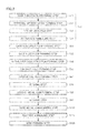
Fig. 2 is a flowchart schematically showing a method for manufacturing the MOSFET. -
Fig. 3 is a schematic cross sectional view for illustrating the method for manufacturing the MOSFET. -
Fig. 4 is a schematic cross sectional view for illustrating the method for manufacturing the MOSFET. -
Fig. 5 is a schematic cross sectional view for illustrating the method for manufacturing the MOSFET. -
Fig. 6 is a schematic cross sectional view for illustrating the method for manufacturing the MOSFET. -
Fig. 7 is a schematic cross sectional view for illustrating the method for manufacturing the MOSFET. -
Fig. 8 is a schematic cross sectional view for illustrating the method for manufacturing the MOSFET. -
Fig. 9 is a schematic cross sectional view for illustrating the method for manufacturing the MOSFET. -
Fig. 10 is a schematic cross sectional view for illustrating the method for manufacturing the MOSFET. -
Fig. 11 is a schematic cross sectional view for illustrating the method for manufacturing the MOSFET. -
Fig. 12 is an enlarged view schematically showing a structure of a second metal film inFig. 11 . -
Fig. 13 is a schematic cross sectional view for illustrating the method for manufacturing the MOSFET. - The following describes an embodiment of the present invention with reference to figures. It should be noted that in the below-mentioned figures, the same or corresponding portions are given the same reference characters and are not described repeatedly.
- First, the following describes a structure of a MOSFET 1 serving as a semiconductor device according to the present embodiment. Referring to
Fig. 1 , MOSFET 1 includes asubstrate 10 made of silicon carbide,gate insulating films 20,gate electrodes 30, interlayerinsulating films 40,source electrodes 50, asource wire 60, and adrain electrode 70.Substrate 10 includes abase substrate 11 and asemiconductor layer 12. Insemiconductor layer 12, adrift region 13,body regions 14,source regions 15, andcontact regions 16 are formed. Further, in MOSFET 1,contact holes 80 are formed to extend throughgate insulating film 20 and interlayer insulatingfilm 40 and expose amain surface 10A ofsubstrate 10. -
Base substrate 11 contains an n type impurity such as N (nitrogen) and therefore has n type conductivity (first conductivity type). Driftregion 13 is an epitaxial growth layer formed on amain surface 11A ofbase substrate 11. As withbase substrate 11,drift region 13 contains an n type impurity such as N (nitrogen), and therefore has n type conductivity. The concentration thereof indrift region 13 is lower than that inbase substrate 11. -
Body regions 14 includemain surface 10A ofsubstrate 10, and are formed to be separated from each other insemiconductor layer 12. Each ofbody regions 14 contains a p type impurity such as Al (aluminum) or B (boron), and therefore has p type conductivity (second conductivity type). -
Source regions 15 includemain surface 10A, and are formed inbody regions 14 such that they are surrounded bybody regions 14. Each ofsource regions 15 contains an n type impurity such as P (phosphorus), and therefore has n type conductivity as withbase substrate 11 anddrift region 13. Further, the concentration of the n type impurity insource region 15 is higher than the concentration of the n type impurity indrift region 13. - As with
source region 15,contact regions 16 includemain surface 10A, are surrounded bybody regions 14, and are respectively formed inbody regions 14 so as to be adjacent to sourceregions 15. As withbody region 14, each ofcontact regions 16 contains a p type impurity such as Al (aluminum) or B (boron) and therefore has p type conductivity. The concentration thereof incontact region 16 is higher than that inbody region 14. - Each of
gate insulating films 20 is made of, for example, SiO2 (silicon dioxide), is formed to be disposed on and in contact withmain surface 10A and extend from the upper surface of onesource region 15 to the upper surface of theother source region 15. - Each of
gate electrodes 30 is disposed on and in contact withgate insulating film 20, and is formed to extend from onesource region 15 to theother source region 15.Gate electrode 30 is made of a conductor such as polysilicon having an impurity added therein, for example. -
Interlayer insulating film 40 is made of for example, SiO2 (silicon dioxide), and is formed ongate insulating film 20 to surroundgate electrode 30. Each of contact holes 80 has side wall surfaces 80A and abottom surface 80B, and is formed to extend throughinterlayer insulating film 40 andgate insulating film 20. Further, as shown inFig. 1 , each of side wall surfaces 80A ofcontact hole 80 is constituted ofinterlayer insulating film 40 andgate insulating film 20, andbottom surface 80B thereof corresponds to the upper surfaces ofsource region 15 andcontact region 16. - In
contact hole 80,source electrode 50 is formed on and in contact withside wall surface 80A andbottom surface 80B. Further,source electrode 50 is made of an alloy containing Ti, Al, and Si, such as a TiAlSi alloy, and is electrically connected to sourceregion 15. -
Drain electrode 70 is formed on amain surface 11B ofbase substrate 11 opposite tomain surface 11 A thereof. As withsource electrode 50,drain electrode 70 is made of, for example, a TiAlSi alloy, and is electrically connected tobase substrate 11. -
Source wire 60 is formed to coversource electrode 50 andinterlayer insulating film 40.Source wire 60 is made of a metal such as Al (aluminum), and is electrically connected to sourceregion 15 viasource electrode 50. - The following describes an operation of MOSFET 1 serving as the semiconductor device according to the present embodiment. Referring to
Fig. 1 , when a voltage is applied betweensource electrode 50 anddrain electrode 70 while an applied voltage togate electrode 30 is smaller than a threshold voltage, i.e., while it is in OFF state, a pn junction formed betweenbody region 14 and driftregion 13 is reverse-biased. Accordingly, MOSFET 1 is in the non-conductive state. Meanwhile, whengate electrode 30 is fed with a voltage equal to or greater than the threshold voltage, an inversion layer is formed inbody region 14. As a result,source region 15 and driftregion 13 are electrically connected to each other, whereby a current flows betweensource electrode 50 anddrain electrode 70. In the manner described above, MOSFET 1 operates. - The following describes a method for manufacturing the semiconductor device in one embodiment of the present invention with reference to
Fig. 1 to Fig. 13 . In the method for manufacturing the semiconductor device in the present embodiment, MOSFET 1 serving as the semiconductor device according to the present embodiment is manufactured. Referring toFig. 2 , a substrate preparing step (S10) is first performed. In this step (S10), steps (S11) to (S 14) described below are performed to preparesubstrate 10 made of silicon carbide. - First, as step (S 11), a base substrate preparing step is performed. In this step (S11), referring to
Fig. 3 , an ingot (not shown) made of, for example, 4H-SiC is sliced to preparebase substrate 11 having n type conductivity. - Next, as a step (S12), an epitaxial growth layer forming step is performed. In this step (S12), referring to
Fig. 3 ,semiconductor layer 12 having n type conductivity is formed by epitaxial growth onmain surface 11 A ofbase substrate 11. - Next, as step (S 13), an ion implantation step is performed. In this step (S 13), referring to
Fig. 4 , for example, Al ions are first implanted into regions includingmain surface 10A ofsubstrate 10, thereby formingbody regions 14 of p type conductivity insemiconductor layer 12. Next, for example, P ions are implanted into each ofbody regions 14 at a depth shallower than the depth in which the Al ions have been implanted, thereby formingsource region 15 of n type conductivity. Then, for example, Al ions are further implanted intobody region 14, thereby formingcontact region 16 adjacent to sourceregion 15, having the same depth as that ofsource region 15, and having p type conductivity. Further, insemiconductor layer 12, a region in which none ofbody region 14,source region 15, andcontact region 16 is formed serves asdrift region 13. - Next, as step (S 14), an activation annealing step is performed. In this step (S14), by
heating substrate 10, the impurities implanted in step (S13) are activated. Accordingly, desired carriers are generated in the regions having the impurities implanted therein. In this way, by performing steps (S11) to (S 14),substrate 10 is prepared in which an active region is formed by the implantation of the impurities. - Next, as a step (S20), a gate insulating film forming step is performed. In this step (S20), referring to
Fig. 5 , for example, byheating substrate 10 in an atmosphere containing oxygen,gate insulating film 20 made of SiO2 (silicon dioxide) is formed to covermain surface 10A ofsubstrate 10. - Next, as a step (S30), a gate electrode forming step is performed. In this step (S30), referring to
Fig. 6 , for example, an LPCVD (Low Pressure Chemical Vapor Deposition) method is employed to formgate electrode 30, which is made of polysilicon containing an impurity, ongate insulating film 20. - Next, as a step (S40), an interlayer insulating film forming step is performed. In this step (S40), referring to
Fig. 7 , for example, a P (Plasma)-CVD method is employed to form interlayer insulatingfilm 40 made of SiO2 (silicon dioxide) ongate insulating film 20 such thatinterlayer insulating film 40 andgate insulating film 20surround gate electrode 30. - Next, as a step (S50), a contact hole forming step is performed. In this step (S50), referring to
Fig. 8 ,contact hole 80 is formed to haveside wall surface 80A andbottom surface 80B and exposemain surface 10A ofsubstrate 10. Specifically, for example, an etching method such as RIE (Reactive Ion Etching) is employed to etch throughinterlayer insulating film 40 andgate insulating film 20, thereby formingcontact hole 80 exposingmain surface 10A of substrate 10 (the upper surfaces ofsource region 15 and contact region 16). Further, in this step (S50),contact hole 80 is formed to be separated fromgate electrode 30. Hence, as shown inFig. 8 ,gate electrode 30 is maintained to be surrounded bygate insulating film 20 andinterlayer insulating film 40. - Next, as a step (S60), a first metal film forming step is performed. In this step (S60), referring to
Fig. 9 , for example, sputtering is performed to form afirst metal film 51 onside wall surface 80A andbottom surface 80B ofcontact hole 80 and the upper surface ofinterlayer insulating film 40. Formed in this step (S60) isfirst metal film 51 containing at least one of Ti and Si and containing no Al, such asfirst metal film 51 made of Ti or Si,first metal film 51 formed of a mixed film of Ti and Si, or afirst metal film 51 formed of a stacked film of Ti and Si. - Next, as a step (S70), an etching step is performed. In this step (S70), as indicated by arrows in
Fig. 10 , dry etching is performed from the side ofmain surface 10A ofsubstrate 10, thereby removingfirst metal film 51 from the upper surface ofinterlayer insulating film 40 andbottom surface 80B ofcontact hole 80 whilefirst metal film 51 remains onside wall surface 80A ofcontact hole 80. - Next, as a step (S80), a second metal film forming step is performed. In this step (S80), a
second metal film 52 containing Ti, Al, and Si is formed on and in contact withfirst metal film 51. Specifically, referring toFig. 11 and Fig. 12 , for example, sputtering is performed to formsecond metal film 52 structured to include afirst metal layer 52a, asecond metal layer 52b, and athird metal layer 52c stacked on one another.First metal layer 52a contains Ti.Second metal layer 52b is on and in contact withfirst metal layer 52a and contains Al.Third metal layer 52c is on and in contact withsecond metal layer 52b and contains Si. Further, in this step (S80), as described above, asecond metal film 52 formed of a stacked film of first tothird metal layers 52a, b, c may be formed, or asecond metal film 52 in which Ti, Al, and Si are mixed by simultaneously sputtering Ti, Al, and Si may be formed. - Next, as a step (S90), an etching step is performed. In this step (S90), as indicated by arrows in
Fig. 13 , dry etching is performed from the side ofmain surface 10A ofsubstrate 10, thereby mainly removingsecond metal film 52 from the upper surface ofinterlayer insulating film 40 whilesecond metal film 52 on and in contact withfirst metal film 51 andbottom surface 80B ofcontact hole 80 remains. - Next, as a step (S100), a third metal film forming step is performed. In this step (S100), referring to
Fig. 13 , as withsecond metal film 52, athird metal film 71 made of, for example, Ti, Al, and Si is formed onmain surface 11B ofbase substrate 11. - Next, as a step (S110), an alloying annealing step is performed. In this step (S100), referring to
Fig. 1 , first andsecond metal films third metal film 71 formed in step (S100) are heated. Accordingly, Ti, Al, and Si are alloyed, thereby formingsource electrodes 50 anddrain electrode 70 each made of a TiAlSi alloy. - Next, as a step (S120), a wire forming step is performed. In this step (S120), referring to
Fig. 1 , for example, a deposition method is employed to formsource wire 60, which is made of a conductor such as Al, on and in contact withsource electrode 50. By performing steps (S10) to (S120), MOSFET 1 is manufactured, thus completing the method for manufacturing the semiconductor device in the present embodiment. - As described above, in the method for manufacturing the semiconductor device in the present embodiment,
source electrode 50 containing Al is formed in the following manner. First,contact hole 80 is formed to extend throughinterlayer insulating film 40 surroundinggate electrode 30, andfirst metal film 51 containing at least one of Ti and Si is formed on and in contact withside wall surface 80A ofcontact hole 80. Next,second metal film 52 containing Ti, Al, and Si is formed on and in contact withfirst metal film 51. Then, by heating first andsecond metal films source electrode 50 containing Ti, Al, and Si is formed. Thus, in the method for manufacturing the semiconductor device in the present embodiment, adhesion betweensource electrode 50 andinterlayer insulating film 40 can be improved by formingfirst metal film 51, which contains at least one of Ti and Si, in advance on and in contact withside wall surface 80A ofcontact hole 80. Hence, according to the method for manufacturing the semiconductor device in the present embodiment, MOSFET 1 having a stable characteristic can be manufactured by improving adhesion betweensource electrode 50 containing aluminum andinterlayer insulating film 40. - Further, in step (S80) of the present embodiment,
second metal film 52 is formed in contact withmain surface 10A ofsubstrate 10 exposed by formingcontact hole 80, butfirst metal film 51 may remain to covermain surface 10A. However, by formingsecond metal film 52 securely in contact withmain surface 10A ofsubstrate 10 as in the present embodiment, a composition ratio of Ti, Al, and Si insecond metal film 52 can be readily adjusted. As a result, MOSFET 1 having a stable characteristic can be manufactured more readily. - Further, in step (S60) of the present embodiment,
first metal film 51 may be formed to have a thickness of not less than 0.1 µm and not more than 1 µm. Thus, the thickness offirst metal film 51 can be set in a range necessary and sufficient to improve adhesion betweensource electrode 50 andinterlayer insulating film 40. - Further, in step (S60) of the present embodiment,
first metal film 51 may be formed to contain Ti and contain no Al. In this way, the adhesion betweensource electrode 50 andinterlayer insulating film 40 can be further improved. - Further, in the present embodiment, in the case of an IGBT, an emitter electrode can be employed as an electrode having a function of supplying carriers, as with
source electrode 50 described above, for example. - The embodiments disclosed herein are illustrative and non-restrictive in any respect. The scope of the present invention is defined by the terms of the claims, rather than the embodiments described above, and is intended to include any modifications within the scope and meaning equivalent to the terms of the claims.
- The method for manufacturing the semiconductor device in the present invention can be particularly advantageously applied to a method for manufacturing a semiconductor device, which is required to manufacture a semiconductor device having a stable characteristic, by improving adhesion between an electrode containing aluminum and an interlayer insulating film.
- 1: MOSFET; 10: substrate; 11: base substrate; 10A, 11A, 11B: main surface; 12: semiconductor layer; 13: drift region; 14: body region; 15: source region; 16: contact region; 20: gate insulating film; 30: gate electrode; 40: interlayer insulating film; 50: source electrode; 51: first metal film; 52: second metal film; 52a: first metal layer; 52b: second metal layer; 52c: third metal layer; 60: source wire; 70: drain electrode; 71: third metal film; 80: contact hole; 80A: side wall surface; 80B: bottom surface.
Claims (6)
- A method for manufacturing a semiconductor device comprising the steps of:preparing a substrate (10) made of silicon carbide;forming a gate insulating film (20) on a surface (10A) of said substrate (10);forming a gate electrode (30) on said gate insulating film (20);forming an interlayer insulating film (40) on said gate insulating film (20) so as to surround said gate electrode (30);forming a contact hole (80) extending through said interlayer insulating film (40) to expose said surface (10A) of said substrate (10) and separated from said gate electrode (30);forming a first metal film (51) on and in contact with a side wall surface (80A) of said contact hole (80), said first metal film (51) containing at least one of Ti and Si and containing no Al;forming a second metal film (52) containing Ti, Al, and Si on and in contact with said first metal film (51); andforming a source electrode (50) containing Ti, Al, and Si by heating said first and second metal films (51, 52).
- The method for manufacturing the semiconductor device according to claim 1, wherein in the step of forming said second metal film (52), said second metal film (52) is formed in contact with said surface (10A) of said substrate (10) exposed by forming said contact hole (80).
- The method for manufacturing the semiconductor device according to claim 1 or 2, wherein in the step of forming said second metal film (52), said second metal film (52) is formed to have a first metal layer (52a), a second metal layer (52b), and a third metal layer (52c) stacked on one another, said first metal layer (52a) containing Ti, said second metal layer (52b) being on and in contact with said first metal layer (52a) and containing Al, said third metal layer (52c) being on and in contact with said second metal layer (52b) and containing Si.
- The method for manufacturing the semiconductor device according to claim 1 or 2, wherein in the step of forming said second metal film (52), said second metal film (52) is formed to contain Ti, Al, and Si mixed with one another.
- The method for manufacturing the semiconductor device according to any one of claims 1-4, wherein in the step of forming said first metal film (51), said first metal film (51) is formed to have a thickness of not less than 0.1 µm and not more than 1 µm.
- The method for manufacturing the semiconductor device according to any one of claims 1-5, wherein in the step of forming said first metal film (51), said first metal film (51) is formed to contain Ti and contain no Al.
Applications Claiming Priority (2)
| Application Number | Priority Date | Filing Date | Title |
|---|---|---|---|
| JP2011270857A JP2013122982A (en) | 2011-12-12 | 2011-12-12 | Semiconductor device manufacturing method |
| PCT/JP2012/078300 WO2013088855A1 (en) | 2011-12-12 | 2012-11-01 | Method for manufacturing semiconductor device |
Publications (1)
| Publication Number | Publication Date |
|---|---|
| EP2793252A1 true EP2793252A1 (en) | 2014-10-22 |
Family
ID=48572358
Family Applications (1)
| Application Number | Title | Priority Date | Filing Date |
|---|---|---|---|
| EP12857979.4A Withdrawn EP2793252A1 (en) | 2011-12-12 | 2012-11-01 | Method for manufacturing semiconductor device |
Country Status (5)
| Country | Link |
|---|---|
| US (1) | US20130149853A1 (en) |
| EP (1) | EP2793252A1 (en) |
| JP (1) | JP2013122982A (en) |
| CN (1) | CN103918062A (en) |
| WO (1) | WO2013088855A1 (en) |
Families Citing this family (5)
| Publication number | Priority date | Publication date | Assignee | Title |
|---|---|---|---|---|
| JP2014038899A (en) * | 2012-08-13 | 2014-02-27 | Sumitomo Electric Ind Ltd | Silicon carbide semiconductor device and method for manufacturing the same |
| US10453923B2 (en) * | 2016-03-16 | 2019-10-22 | Fuji Electric Co., Ltd. | Silicon carbide semiconductor device and method of manufacturing silicon carbide semiconductor device |
| JP6716985B2 (en) * | 2016-03-16 | 2020-07-01 | 富士電機株式会社 | Semiconductor device and method of manufacturing semiconductor device |
| WO2018056233A1 (en) * | 2016-09-20 | 2018-03-29 | 富士電機株式会社 | Semiconductor device and method for manufacturing semiconductor device |
| CN112086367A (en) * | 2020-09-27 | 2020-12-15 | 江苏东海半导体科技有限公司 | TO-220 packaged MOSFET with Clip structure and manufacturing method thereof |
Family Cites Families (7)
| Publication number | Priority date | Publication date | Assignee | Title |
|---|---|---|---|---|
| JP4003296B2 (en) | 1998-06-22 | 2007-11-07 | 株式会社デンソー | Silicon carbide semiconductor device and manufacturing method thereof |
| JP3559971B2 (en) | 2001-12-11 | 2004-09-02 | 日産自動車株式会社 | Silicon carbide semiconductor device and method of manufacturing the same |
| JP2009194127A (en) * | 2008-02-14 | 2009-08-27 | Panasonic Corp | Semiconductor device and manufacturing method thereof |
| CN102007595B (en) * | 2008-04-15 | 2013-12-25 | 住友电气工业株式会社 | Semiconductor device and method of manufacturing same |
| JP2010238738A (en) * | 2009-03-30 | 2010-10-21 | Toshiba Corp | Semiconductor device and manufacturing method of semiconductor device |
| JP4858791B2 (en) * | 2009-05-22 | 2012-01-18 | 住友電気工業株式会社 | Semiconductor device and manufacturing method thereof |
| CN102227812A (en) * | 2009-10-05 | 2011-10-26 | 住友电气工业株式会社 | Semiconductor device |
-
2011
- 2011-12-12 JP JP2011270857A patent/JP2013122982A/en active Pending
-
2012
- 2012-11-01 CN CN201280054324.2A patent/CN103918062A/en active Pending
- 2012-11-01 WO PCT/JP2012/078300 patent/WO2013088855A1/en not_active Ceased
- 2012-11-01 EP EP12857979.4A patent/EP2793252A1/en not_active Withdrawn
- 2012-11-09 US US13/673,741 patent/US20130149853A1/en not_active Abandoned
Non-Patent Citations (1)
| Title |
|---|
| See references of WO2013088855A1 * |
Also Published As
| Publication number | Publication date |
|---|---|
| JP2013122982A (en) | 2013-06-20 |
| CN103918062A (en) | 2014-07-09 |
| WO2013088855A1 (en) | 2013-06-20 |
| US20130149853A1 (en) | 2013-06-13 |
Similar Documents
| Publication | Publication Date | Title |
|---|---|---|
| EP2849231B1 (en) | Semiconductor device and method for manufacturing same | |
| US9099553B2 (en) | Semiconductor device and method for manufacturing same | |
| EP2966676B1 (en) | Silicon-carbide semiconductor device and manufacturing method therefor | |
| US20130292702A1 (en) | Semiconductor device and method for manufacturing same | |
| US9263527B2 (en) | Silicon carbide semiconductor device and method of manufacturing same | |
| EP2736067A1 (en) | Method for manufacturing semiconductor device | |
| US20150287817A1 (en) | Silicon carbide semiconductor device and method for manufacturing same | |
| KR20130109168A (en) | Method of manufacturing silicon carbide semiconductor device | |
| US9472635B2 (en) | Silicon carbide semiconductor device | |
| JP2015076592A (en) | Silicon carbide semiconductor device and manufacturing method of the same | |
| EP2784825B1 (en) | Semiconductor device and method for manufacturing same | |
| JP2014175470A (en) | Silicon carbide semiconductor device manufacturing method | |
| US20130149853A1 (en) | Method for manufacturing semiconductor device | |
| US20140103365A1 (en) | Semiconductor device and method for manufacturing same | |
| JP2015204409A (en) | Silicon carbide semiconductor device and manufacturing method of the same | |
| US8829605B2 (en) | Semiconductor device having deep and shallow trenches | |
| US8802552B2 (en) | Method for manufacturing semiconductor device |
Legal Events
| Date | Code | Title | Description |
|---|---|---|---|
| PUAI | Public reference made under article 153(3) epc to a published international application that has entered the european phase |
Free format text: ORIGINAL CODE: 0009012 |
|
| 17P | Request for examination filed |
Effective date: 20140409 |
|
| AK | Designated contracting states |
Kind code of ref document: A1 Designated state(s): AL AT BE BG CH CY CZ DE DK EE ES FI FR GB GR HR HU IE IS IT LI LT LU LV MC MK MT NL NO PL PT RO RS SE SI SK SM TR |
|
| STAA | Information on the status of an ep patent application or granted ep patent |
Free format text: STATUS: THE APPLICATION HAS BEEN WITHDRAWN |
|
| DAX | Request for extension of the european patent (deleted) | ||
| 18W | Application withdrawn |
Effective date: 20150309 |