EP2792016B1 - Übergangsschaltung zwischen mikrostreifenleitung und schlitzleitung - Google Patents
Übergangsschaltung zwischen mikrostreifenleitung und schlitzleitung Download PDFInfo
- Publication number
- EP2792016B1 EP2792016B1 EP12795473.3A EP12795473A EP2792016B1 EP 2792016 B1 EP2792016 B1 EP 2792016B1 EP 12795473 A EP12795473 A EP 12795473A EP 2792016 B1 EP2792016 B1 EP 2792016B1
- Authority
- EP
- European Patent Office
- Prior art keywords
- circuit
- microstrip line
- transition
- impedance
- slot
- Prior art date
- Legal status (The legal status is an assumption and is not a legal conclusion. Google has not performed a legal analysis and makes no representation as to the accuracy of the status listed.)
- Not-in-force
Links
- 230000007704 transition Effects 0.000 title claims description 70
- 230000008878 coupling Effects 0.000 claims description 37
- 238000010168 coupling process Methods 0.000 claims description 37
- 238000005859 coupling reaction Methods 0.000 claims description 37
- 238000001914 filtration Methods 0.000 claims description 14
- 239000000758 substrate Substances 0.000 claims description 10
- 230000001419 dependent effect Effects 0.000 claims 1
- 230000004044 response Effects 0.000 description 23
- 230000005540 biological transmission Effects 0.000 description 16
- 238000003780 insertion Methods 0.000 description 13
- 230000037431 insertion Effects 0.000 description 13
- 238000005516 engineering process Methods 0.000 description 7
- 230000008901 benefit Effects 0.000 description 4
- 230000005284 excitation Effects 0.000 description 4
- 230000002452 interceptive effect Effects 0.000 description 4
- 238000004891 communication Methods 0.000 description 3
- 235000021183 entrée Nutrition 0.000 description 3
- 230000003071 parasitic effect Effects 0.000 description 3
- 241001644893 Entandrophragma utile Species 0.000 description 2
- 240000008042 Zea mays Species 0.000 description 2
- 210000004027 cell Anatomy 0.000 description 2
- 238000010586 diagram Methods 0.000 description 2
- 230000003993 interaction Effects 0.000 description 2
- 238000004088 simulation Methods 0.000 description 2
- 238000012546 transfer Methods 0.000 description 2
- 238000013459 approach Methods 0.000 description 1
- 230000000593 degrading effect Effects 0.000 description 1
- 238000004519 manufacturing process Methods 0.000 description 1
- 239000000463 material Substances 0.000 description 1
- 238000000034 method Methods 0.000 description 1
- 238000012986 modification Methods 0.000 description 1
- 230000004048 modification Effects 0.000 description 1
- 244000045947 parasite Species 0.000 description 1
Images


Classifications
-
- H—ELECTRICITY
- H01—ELECTRIC ELEMENTS
- H01P—WAVEGUIDES; RESONATORS, LINES, OR OTHER DEVICES OF THE WAVEGUIDE TYPE
- H01P1/00—Auxiliary devices
- H01P1/20—Frequency-selective devices, e.g. filters
- H01P1/201—Filters for transverse electromagnetic waves
- H01P1/203—Strip line filters
- H01P1/2039—Galvanic coupling between Input/Output
-
- H—ELECTRICITY
- H01—ELECTRIC ELEMENTS
- H01P—WAVEGUIDES; RESONATORS, LINES, OR OTHER DEVICES OF THE WAVEGUIDE TYPE
- H01P5/00—Coupling devices of the waveguide type
- H01P5/08—Coupling devices of the waveguide type for linking dissimilar lines or devices
- H01P5/10—Coupling devices of the waveguide type for linking dissimilar lines or devices for coupling balanced lines or devices with unbalanced lines or devices
- H01P5/1007—Microstrip transitions to Slotline or finline
-
- H—ELECTRICITY
- H01—ELECTRIC ELEMENTS
- H01P—WAVEGUIDES; RESONATORS, LINES, OR OTHER DEVICES OF THE WAVEGUIDE TYPE
- H01P1/00—Auxiliary devices
- H01P1/24—Terminating devices
- H01P1/26—Dissipative terminations
- H01P1/268—Strip line terminations
Definitions
- the present invention relates to a transition circuit from a microstrip line to a slot line.
- the invention finds application in the field of radiocommunications and in particular in the field of multistandard multimode user terminals working in near frequency bands.
- Multistandard multi-mode user terminals integrate multiple radiocommunication or wireless communication systems and experience strong interference due, on the one hand, to the proximity of the frequency bands allocated to the different systems and, on the other hand, to the proximity antenna physics, the size of the terminals being more and more reduced. This results in harmful parasitic interactions between the different systems.
- a first known solution is to introduce, within the terminal, a frequency-selective filter in the transmission-reception chain of each of the systems, this filter being intended to reject unwanted frequencies for the system considered. , such as parasitic lines from other systems, and / or parasites from the transmission / reception chain in question and / or harmonics.
- these filters being very severe (very low insertion losses, high selectivity and very narrow bandwidth), they can not currently be made in a low-cost technology, for example with printed circuits. based on FR4 type substrate.
- An object of the invention is to provide a microstrip line / slot line transition circuit capable of filtering unwanted frequencies without degrading the performance of the transition circuit in its useful band.
- Another object of the invention is to provide such a transition circuit that is feasible in a low cost technology.
- the subject of the invention is a transition circuit from a microstrip line to a slot line comprising a substrate provided with a ground plane, a microstrip line formed on said substrate at a predetermined distance from the ground plane, and extending from a first input / output port, and a slot made in the ground plane forming a slot line extending substantially perpendicular to said microstrip line to a second input / output port and intersecting said microstrip line in a so-called coupling zone of the transition circuit, said line microstrip having a first microstrip line portion for transmitting a signal between the first input / output port and the coupling area, and a second microstrip line portion, said slot line having a first slit line portion for transmitting said signal between the coupling area and the second input / output port, and a second slot line portion.
- the slot line comprises a first filter circuit connected to the coupling zone via said second slot line portion, said first filter circuit and said second slot line portion being adapted to return to the slot line, to the level of the coupling zone, an impedance substantially equal to the impedance of an open circuit for at least one desired frequency of the signal and an impedance substantially equal to the impedance of a short circuit for at least one undesired frequency of the signal .
- a filter circuit connected to the second slot line portion is used to reflect, by reflection, optimal electromagnetic coupling conditions on the slot line at the coupling area of the transition circuit for the desired frequency and quasi-zero electromagnetic coupling conditions for the unwanted frequency.
- a filtering circuit is also connected to the second slot line portion to reflect, by reflection, optimal electromagnetic coupling conditions on the microstrip line at the coupling area of the transition circuit for the desired frequency and quasi-zero electromagnetic coupling conditions for the unwanted frequency.
- the microstrip line then comprises a second filter circuit connected to the zone of coupling via said second microstrip line portion, said second filter circuit and said second microstrip line portion adapted to return to the microstrip line, at the coupling area, an impedance substantially equal to the impedance of a short circuit for said at least one desired frequency and an impedance substantially equal to the open circuit impedance for said at least one undesired frequency.
- the first filtering circuit arranged on the slot line is a filter connected to a load resistor and able to reject the said at least one desired frequency and to pass the said at least one undesirable frequency and the second portion slot line substantially corresponds to a quarter-wave slot line for said at least one desired frequency.
- the second filter circuit disposed on the microstrip line is a filter connected to a load resistor and able to reject the said at least one desired frequency and to pass the said at least one undesired frequency and the second microstrip line portion corresponds to substantially to a quarter wave microstrip line for said at least one desired frequency.
- the first and second filter circuits are notch filters rejecting said at least one desired frequency and passing said at least one undesirable frequency.
- the first and second filtering circuits are bandpass filters passing said at least one unwanted frequency and rejecting said at least one desired frequency.
- the transition circuit is made in a low-cost technology, for example by producing the circuit on a FR4-type substrate.
- the invention also relates to a multistandard terminal comprising at least one transition circuit as described above.
- the Figures 1 to 3 present a conventional microstrip / line line transition circuit Knorr type.
- the transition circuit is formed on a substrate S provided with a ground plane. It comprises a microstrip line 1 and a slot line 2 etched in the ground plane, the microstrip line being disposed at a predetermined distance from the ground plane.
- the microstrip line 1 ends, at a first end 1a, by an input port P1 and at a second end 1b by an open circuit CO.
- the slot line 2 terminates, at a first end 2a, by a short circuit CC and, at a second end 2b, by an output port P2.
- Port P1 is connected to a transmission chain and port P2 is connected to a slotted antenna.
- the microstrip line 1 extends substantially perpendicular to the slot line 2 and the two lines intersect in a so-called coupling zone Z of the transition circuit.
- the microstrip line 1 comprises a portion 11 of microstrip line connected to the port P1 extending by a portion 12 of microstrip line, said coupling portion, disposed above the slot line 2, said coupling portion 12 extending there even by a portion 13 terminating in an open circuit.
- the slot line 2 comprises a portion 21 of slot line connected to the port P2 extending through a slot line portion 22, said coupling portion, disposed below the microstrip line 1, said coupling portion 22 is extending itself by a portion 23 ending in a short circuit CC.
- Portions 12 and 22 define the Z coupling zone mentioned above. The transfer of energy from the port P1 to the port P2 is by electromagnetic coupling of the portions 12 and 22.
- microstrip line has been hatched to better distinguish it from the slit line. Similarly, to better distinguish the different portions of each of the lines, they have separated and connected features that in reality do not exist.
- the portions 13 and 23 In order to obtain optimum electromagnetic coupling conditions between the microstrip line 1 and the slot line 2, the portions 13 and 23 must respectively bring back a short circuit and an open circuit at the level of the transition zone Z.
- the length of the portion 13 must be substantially equal to ⁇ m1 / 4 where ⁇ m1 is the guided wavelength in the microstrip line associated with a desired frequency f1 (working frequency of the transition circuit).
- the length of the portion 23 must be substantially equal to ⁇ f1 / 4 where ⁇ f1 is the guided wavelength in the slot line associated with the desired frequency f1.
- the portions 11 and 21 have the function of reducing, respectively to the ports P1 and P2, an impedance close to that present at the ports P1 and P2, generally 50 ohms for P1 and of the order of 80-100 ohms for the port P2.
- this transition circuit from a microstrip line to a slot line is applicable to operation in the 5GHz WiFi band. It was made on a multilayer substrate based on FR4 material at very low cost.
- a microstrip line / frequency selective slit line transition is proposed, capable of passing desired frequencies contained in a useful band and of rejecting frequencies outside this useful band.
- the role of filters is to provide the desired selectivity by level of the coupling zone Z the optimum coupling conditions, ie a short-circuit (respectively an open circuit) for the microstrip line (respectively slot line) in the useful band of the transition.
- a short-circuit ie an open circuit
- the microstrip line ie slot line
- the purpose of the line portions 13 and 23 is to reduce the impedances of the inputs C and D of the filters to the impedances required at the coupling zone in order to favor the maximum power transfer in the useful band from port P1 to port P2 and according to the KNORR principle, namely a zero impedance (short circuit) in B and an infinite impedance (open circuit) in A.
- the impedance levels sought at the coupling zone outside and in the useful band of the transition namely: the characteristic impedances and the lengths of the portions of the line 13 and 23, the load resistances Rm and Rs, the impedances of the intrinsic elements to each of the SBFm and SBFs filters.
- the line portion 11 serves, if necessary, to reduce the impedance at the port P1 to the usual value of 50 ohms.
- the transition circuit of the figure 4 was simulated using Agilent / ADS software for a filter transition allowing the band 5 to 6 GHz to pass.
- the coupling of the portion 12 of the microstrip line with the portion 22 of the slot line was modeled with the Agilent / Momentum electromagnetic simulator to extract the parameters S.
- a simulation of the circuit was performed by taking for the other components of the circuit, namely the other portions of the line and the charged filters, their electrical equivalent model, thus disregarding their technique and production technology.
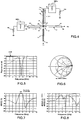
- the responses of a SBFm filter thus defined are illustrated by the Figures 5 and 6 .
- the figure 5 shows the insertion losses, the bandwidth and the rejection level and the figure 6 shows that this SBFm filter has an open-circuit at its inputs at the center frequency of 5.5 GHz.
- the reflection response of the notch filter is that of a bandpass filter, passing the band from 5 to 6 GHz.
- This inverse (reflected) response and its advantages are exploited by the invention.
- the 2 filters of the circuit are of order 2 and have theoretical insertion losses of 2dB.
- the parameters of the integrated components of the circuit of the figure 4 are given in the table below. They have been optimized to meet the requirements to achieve the desired performance.
- the following performances are obtained for the transition circuit.
- the figure 7 shows the transmission response of the transition and the figure 8 shows the answers in reflection.
- the transmission response is of the bandpass type with a bandwidth ranging from 5 to 6GHz. In the immediate vicinity of this band, the signal is rejected by more than 20dB.
- the transition is also well suited in the bandwidth, with reflection levels below -12dB.
- the excitation port P1 is also well adapted (dB (S11)). This shows that the signal is not reflected and is transmitted to a load, in this case the load Rm of the notch filter SBFm. This is only possible because, outside of the transition bandwidth, the SBFs slot-notch filter does reduce a very low impedance to the coupling area at point A. This is demonstrated in Figure 9 . In this figure, it can be seen that the notch filter reduces to point A a low impedance close to a short circuit at 3GHz and at 8 GHz (outside the bandwidth) and an open circuit at 5.5 GHz (in bandwidth).
- the transmission response of the transition circuit described above is of the bandpass type, the interfering frequencies to be suppressed being present outside the bandwidth of the circuit.
- the notch filters can be replaced by bandpass filters so as to obtain a response of the notch transition circuit.
- Such a response makes it possible, for example, to reject an interfering signal in a well-identified frequency band.
Landscapes
- Physics & Mathematics (AREA)
- Electromagnetism (AREA)
- Control Of Motors That Do Not Use Commutators (AREA)
Claims (8)
- Übergangsschaltung einer Mikrostreifenleitung zu einer Schlitzleitung, umfassend:- ein Substrat (S), das mit einer Masseplatte versehen ist,- eine Mikrostreifenleitung (1), die auf dem Substrat in einer vorgegebenen Entfernung von der Masseplatte ausgeführt ist und die sich von einem ersten Eingangs-/Ausgangsport (P1) erstreckt, und ein Schlitz, der in der Masseplatte ausgeführt ist, der eine Schlitzleitung (2) bildet, die sich im Wesentlichen senkrecht zu der Mikrostreifenleitung bis zu einem zweiten Eingangs-/Ausgangsport (P2) erstreckt und die Mikrostreifenleitung in einer so genannten Kopplungszone (Z) der Übergangsschaltung kreuzt,wobei die Mikrostreifenleitung einen ersten Abschnitt der Mikrostreifenleitung (11) zur Übertragung eines Signals zwischen dem ersten Eingangs-/Ausgangsport und der Kopplungszone und einen zweiten Abschnitt der Mikrostreifenleitung (13) aufweist,
wobei die Schlitzleitung einen ersten Abschnitt der Schlitzleitung (21) zur Übertragung des Signals zwischen der Kopplungszone und dem zweiten Eingangs-/Ausgangsport und einen zweiten Abschnitt der Schlitzleitung (23) aufweist,
dadurch gekennzeichnet, dass die Schlitzleitung (2) einen ersten Filterkreis (SBFs), der über den zweiten Abschnitt der Schlitzleitung mit der Kopplungszone verbunden ist, aufweist, wobei der erste Filterkreis und der zweite Abschnitt der Schlitzleitung angepasst sind, um eine Impedanz, die für mindestens eine gewünschte Frequenz des Signals im Wesentlichen gleich der Impedanz eines offenen Stromkreises ist, und eine Impedanz, die für mindestens eine unerwünschte Frequenz des Signals im Wesentlichen gleich der Kurzschluss-Impedanz ist, auf der Höhe der Kopplungszone auf die Schlitzleitung zurückzuführen. - Übergangsschaltung nach Anspruch 1, dadurch gekennzeichnet, dass die Mikrostreifenleitung einen zweiten Filterkreis (SBFm), der über den zweiten Abschnitt der Mikrostreifenleitung mit der Kopplungszone verbunden ist, aufweist, wobei der zweite Filterkreis und der zweite Abschnitt der Mikrostreifenleitung angepasst sind, um eine Impedanz, die für mindestens eine gewünschte Frequenz im Wesentlichen gleich der Kurschluss-Impedanz ist, und eine Impedanz, die für mindestens eine unerwünschte Frequenz im Wesentlichen gleich der Impedanz eines offenen Stromkreises ist, auf der Höhe der Kopplungszone auf die Mikrostreifenleitung zurückzuführen.
- Übergangsschaltung nach Anspruch 1 oder 2, dadurch gekennzeichnet, dass der erste Filterkreis ein Filter (SBFs) ist, der mit einem Lastwiderstand (Rs) verbunden ist und geeignet ist, die mindestens eine gewünschte Frequenz zurückzuweisen und die mindestens eine unerwünschte Frequenz durchzulassen, und dass der zweite Abschnitt der Schlitzleitung im Wesentlichen einer Lambda-Viertel-Schlitzleitung für die mindestens eine gewünschte Frequenz entspricht.
- Übergangsschaltung nach Anspruch 3, der wiederum von Anspruch 2 abhängig ist, dadurch gekennzeichnet, dass der zweite Filterkreis ein Filter (SBFm) ist, der mit einem Lastwiderstand (Rm) verbunden ist und geeignet ist, die mindestens eine gewünschte Frequenz zurückzuweisen und die mindestens eine unerwünschte Frequenz durchzulassen, und dass der zweite Abschnitt der Mikrostreifenleitung im Wesentlichen einer Lambda-Viertel-Mikrostreifenleitung für die mindestens eine gewünschte Frequenz entspricht.
- Übergangsschaltung nach Anspruch 4, dadurch gekennzeichnet, dass der erste und der zweite Filterkreis Bandsperrfilter sind.
- Übergangsschaltung nach Anspruch 4, dadurch gekennzeichnet, dass der erste und der zweite Filterkreis Bandpassfilter sind.
- Übergangsschaltung nach einem der vorhergehenden Ansprüche, dadurch gekennzeichnet, dass das Substrat vom Typ FR4 ist.
- Multi-Standard-Terminal, dadurch gekennzeichnet, dass er mindestens eine Übergangsschaltung nach einem der Ansprüche 1 bis 7 aufweist.
Applications Claiming Priority (2)
| Application Number | Priority Date | Filing Date | Title |
|---|---|---|---|
| FR1161437A FR2984018A1 (fr) | 2011-12-12 | 2011-12-12 | Circuit de transition ligne microruban/ligne fente |
| PCT/EP2012/074659 WO2013087509A1 (fr) | 2011-12-12 | 2012-12-06 | Circuit de transition ligne microruban/ligne fente |
Publications (2)
| Publication Number | Publication Date |
|---|---|
| EP2792016A1 EP2792016A1 (de) | 2014-10-22 |
| EP2792016B1 true EP2792016B1 (de) | 2016-03-02 |
Family
ID=47291012
Family Applications (1)
| Application Number | Title | Priority Date | Filing Date |
|---|---|---|---|
| EP12795473.3A Not-in-force EP2792016B1 (de) | 2011-12-12 | 2012-12-06 | Übergangsschaltung zwischen mikrostreifenleitung und schlitzleitung |
Country Status (7)
| Country | Link |
|---|---|
| US (1) | US20150022280A1 (de) |
| EP (1) | EP2792016B1 (de) |
| JP (1) | JP2015505198A (de) |
| KR (1) | KR20140100577A (de) |
| CN (1) | CN103988363B (de) |
| FR (1) | FR2984018A1 (de) |
| WO (1) | WO2013087509A1 (de) |
Families Citing this family (1)
| Publication number | Priority date | Publication date | Assignee | Title |
|---|---|---|---|---|
| CN120581846B (zh) * | 2025-08-04 | 2025-10-10 | 广东工业大学 | 一种双通带的吸收式滤波器 |
Family Cites Families (5)
| Publication number | Priority date | Publication date | Assignee | Title |
|---|---|---|---|---|
| US3760304A (en) * | 1969-05-21 | 1973-09-18 | Us Army | Slot line |
| DE2546836A1 (de) * | 1975-10-18 | 1977-04-21 | Philips Patentverwaltung | Uebergang von einer mikro-streifenleitung auf eine schlitzleitung |
| FR2873857A1 (fr) | 2004-07-28 | 2006-02-03 | Thomson Licensing Sa | Dispositif rayonnant a filtrage de frequence integre et procede de filtrage correspondant |
| FR2960347B1 (fr) * | 2010-05-21 | 2012-07-13 | Thales Sa | Element rayonnant comprenant un dispositif de filtrage, notamment pour un reseau formant une antenne active a balayage electronique |
| CN201946730U (zh) * | 2011-04-11 | 2011-08-24 | 孙向荣 | 一种超宽频带反相功率合成器 |
-
2011
- 2011-12-12 FR FR1161437A patent/FR2984018A1/fr not_active Withdrawn
-
2012
- 2012-12-06 EP EP12795473.3A patent/EP2792016B1/de not_active Not-in-force
- 2012-12-06 CN CN201280061425.2A patent/CN103988363B/zh not_active Expired - Fee Related
- 2012-12-06 KR KR1020147019412A patent/KR20140100577A/ko not_active Withdrawn
- 2012-12-06 JP JP2014546427A patent/JP2015505198A/ja not_active Withdrawn
- 2012-12-06 US US14/362,516 patent/US20150022280A1/en not_active Abandoned
- 2012-12-06 WO PCT/EP2012/074659 patent/WO2013087509A1/fr not_active Ceased
Also Published As
| Publication number | Publication date |
|---|---|
| US20150022280A1 (en) | 2015-01-22 |
| EP2792016A1 (de) | 2014-10-22 |
| KR20140100577A (ko) | 2014-08-14 |
| WO2013087509A1 (fr) | 2013-06-20 |
| FR2984018A1 (fr) | 2013-06-14 |
| JP2015505198A (ja) | 2015-02-16 |
| CN103988363B (zh) | 2016-05-11 |
| CN103988363A (zh) | 2014-08-13 |
Similar Documents
| Publication | Publication Date | Title |
|---|---|---|
| EP1473833B1 (de) | Integrierte zwei-band Induktivität und Anwendungen | |
| EP1427053B1 (de) | Richtkoppler | |
| EP2345104B1 (de) | Differenz-dipolantennensystem mit einer koplanaren strahlungsstruktur und sender-/empfängereinrichtung | |
| EP2483965B1 (de) | Selektivitätsverstärkung für einen dualband-koppler | |
| EP1172929B1 (de) | Rauscharme Verstärkungsanordnung insbesondere für ein zellulares Mobiltelefon | |
| EP3017499A1 (de) | Bandsperrfilter | |
| FR2822301A1 (fr) | Antenne a bande elargie pour appareils mobiles | |
| EP2184801A1 (de) | Vorrichtung zur Abdichtung eines Öffnungsfeldes eines Kraftfahrzeugs mit Hilfe eines Schiebepaneels, und entsprechendes Kraftfahrzeug | |
| FR2942676A1 (fr) | Systeme d'antennes compact a diversite d'ordre 2. | |
| EP1863116A1 (de) | Breitbandrichtkoppler | |
| FR2817661A1 (fr) | Dispositif pour la reception et/ou l'emission de signaux multifaisceaux | |
| FR2999337A1 (fr) | Circuit de transition d'une ligne micro-ruban vers une ligne fente duale bande | |
| FR2802378A1 (fr) | Dispositif a circuit non reciproque et dispositif de telecommunications l'utilisant | |
| EP2466684B1 (de) | Antennenumschaltungssystem | |
| EP1367714A1 (de) | Hochfrequenzkoppler | |
| US6956444B2 (en) | Method and apparatus for rejecting common mode signals on a printed circuit board and method for making same | |
| WO2008049921A1 (fr) | Antenne mono ou multi-frequences | |
| EP2792016B1 (de) | Übergangsschaltung zwischen mikrostreifenleitung und schlitzleitung | |
| EP0015610B1 (de) | Spiegelfrequenzreflektierendes Mikrowellenfilter und Mikrowellenempfänger mit einem solchen Filter | |
| WO2012089619A1 (fr) | Filtre variable par condensateur commute au moyen de composants mems | |
| FR2871618A1 (fr) | Filtre basse-bande hyperfrequence de type finline | |
| WO2013092356A1 (fr) | Carte de test pour carte de circuit imprime dans le domaine des systemes sans fils | |
| EP3644437B1 (de) | Antenne für mobile kommunikationsvorrichtung | |
| WO2006018567A9 (fr) | Dispositif rayonnant a filtrage de frequence integre et procede de filtrage correspondant | |
| EP1548877B1 (de) | Multibandantenne mit planaren Strahlerflächen und tragbares Telefon mit einer derartigen Antenne |
Legal Events
| Date | Code | Title | Description |
|---|---|---|---|
| PUAI | Public reference made under article 153(3) epc to a published international application that has entered the european phase |
Free format text: ORIGINAL CODE: 0009012 |
|
| 17P | Request for examination filed |
Effective date: 20140528 |
|
| AK | Designated contracting states |
Kind code of ref document: A1 Designated state(s): AL AT BE BG CH CY CZ DE DK EE ES FI FR GB GR HR HU IE IS IT LI LT LU LV MC MK MT NL NO PL PT RO RS SE SI SK SM TR |
|
| DAX | Request for extension of the european patent (deleted) | ||
| GRAP | Despatch of communication of intention to grant a patent |
Free format text: ORIGINAL CODE: EPIDOSNIGR1 |
|
| INTG | Intention to grant announced |
Effective date: 20150716 |
|
| GRAS | Grant fee paid |
Free format text: ORIGINAL CODE: EPIDOSNIGR3 |
|
| GRAA | (expected) grant |
Free format text: ORIGINAL CODE: 0009210 |
|
| AK | Designated contracting states |
Kind code of ref document: B1 Designated state(s): AL AT BE BG CH CY CZ DE DK EE ES FI FR GB GR HR HU IE IS IT LI LT LU LV MC MK MT NL NO PL PT RO RS SE SI SK SM TR |
|
| REG | Reference to a national code |
Ref country code: GB Ref legal event code: FG4D Free format text: NOT ENGLISH |
|
| REG | Reference to a national code |
Ref country code: AT Ref legal event code: REF Ref document number: 778574 Country of ref document: AT Kind code of ref document: T Effective date: 20160315 Ref country code: CH Ref legal event code: EP Ref country code: DE Ref legal event code: R084 Ref document number: 602012015284 Country of ref document: DE |
|
| REG | Reference to a national code |
Ref country code: IE Ref legal event code: FG4D Free format text: LANGUAGE OF EP DOCUMENT: FRENCH |
|
| REG | Reference to a national code |
Ref country code: DE Ref legal event code: R096 Ref document number: 602012015284 Country of ref document: DE |
|
| REG | Reference to a national code |
Ref country code: NL Ref legal event code: MP Effective date: 20160302 |
|
| REG | Reference to a national code |
Ref country code: LT Ref legal event code: MG4D |
|
| REG | Reference to a national code |
Ref country code: AT Ref legal event code: MK05 Ref document number: 778574 Country of ref document: AT Kind code of ref document: T Effective date: 20160302 |
|
| PG25 | Lapsed in a contracting state [announced via postgrant information from national office to epo] |
Ref country code: ES Free format text: LAPSE BECAUSE OF FAILURE TO SUBMIT A TRANSLATION OF THE DESCRIPTION OR TO PAY THE FEE WITHIN THE PRESCRIBED TIME-LIMIT Effective date: 20160302 Ref country code: FI Free format text: LAPSE BECAUSE OF FAILURE TO SUBMIT A TRANSLATION OF THE DESCRIPTION OR TO PAY THE FEE WITHIN THE PRESCRIBED TIME-LIMIT Effective date: 20160302 Ref country code: HR Free format text: LAPSE BECAUSE OF FAILURE TO SUBMIT A TRANSLATION OF THE DESCRIPTION OR TO PAY THE FEE WITHIN THE PRESCRIBED TIME-LIMIT Effective date: 20160302 Ref country code: GR Free format text: LAPSE BECAUSE OF FAILURE TO SUBMIT A TRANSLATION OF THE DESCRIPTION OR TO PAY THE FEE WITHIN THE PRESCRIBED TIME-LIMIT Effective date: 20160603 Ref country code: NO Free format text: LAPSE BECAUSE OF FAILURE TO SUBMIT A TRANSLATION OF THE DESCRIPTION OR TO PAY THE FEE WITHIN THE PRESCRIBED TIME-LIMIT Effective date: 20160602 |
|
| PG25 | Lapsed in a contracting state [announced via postgrant information from national office to epo] |
Ref country code: PL Free format text: LAPSE BECAUSE OF FAILURE TO SUBMIT A TRANSLATION OF THE DESCRIPTION OR TO PAY THE FEE WITHIN THE PRESCRIBED TIME-LIMIT Effective date: 20160302 Ref country code: LV Free format text: LAPSE BECAUSE OF FAILURE TO SUBMIT A TRANSLATION OF THE DESCRIPTION OR TO PAY THE FEE WITHIN THE PRESCRIBED TIME-LIMIT Effective date: 20160302 Ref country code: AT Free format text: LAPSE BECAUSE OF FAILURE TO SUBMIT A TRANSLATION OF THE DESCRIPTION OR TO PAY THE FEE WITHIN THE PRESCRIBED TIME-LIMIT Effective date: 20160302 Ref country code: RS Free format text: LAPSE BECAUSE OF FAILURE TO SUBMIT A TRANSLATION OF THE DESCRIPTION OR TO PAY THE FEE WITHIN THE PRESCRIBED TIME-LIMIT Effective date: 20160302 Ref country code: NL Free format text: LAPSE BECAUSE OF FAILURE TO SUBMIT A TRANSLATION OF THE DESCRIPTION OR TO PAY THE FEE WITHIN THE PRESCRIBED TIME-LIMIT Effective date: 20160302 Ref country code: SE Free format text: LAPSE BECAUSE OF FAILURE TO SUBMIT A TRANSLATION OF THE DESCRIPTION OR TO PAY THE FEE WITHIN THE PRESCRIBED TIME-LIMIT Effective date: 20160302 Ref country code: LT Free format text: LAPSE BECAUSE OF FAILURE TO SUBMIT A TRANSLATION OF THE DESCRIPTION OR TO PAY THE FEE WITHIN THE PRESCRIBED TIME-LIMIT Effective date: 20160302 |
|
| PG25 | Lapsed in a contracting state [announced via postgrant information from national office to epo] |
Ref country code: IS Free format text: LAPSE BECAUSE OF FAILURE TO SUBMIT A TRANSLATION OF THE DESCRIPTION OR TO PAY THE FEE WITHIN THE PRESCRIBED TIME-LIMIT Effective date: 20160702 Ref country code: EE Free format text: LAPSE BECAUSE OF FAILURE TO SUBMIT A TRANSLATION OF THE DESCRIPTION OR TO PAY THE FEE WITHIN THE PRESCRIBED TIME-LIMIT Effective date: 20160302 |
|
| PG25 | Lapsed in a contracting state [announced via postgrant information from national office to epo] |
Ref country code: RO Free format text: LAPSE BECAUSE OF FAILURE TO SUBMIT A TRANSLATION OF THE DESCRIPTION OR TO PAY THE FEE WITHIN THE PRESCRIBED TIME-LIMIT Effective date: 20160302 Ref country code: CZ Free format text: LAPSE BECAUSE OF FAILURE TO SUBMIT A TRANSLATION OF THE DESCRIPTION OR TO PAY THE FEE WITHIN THE PRESCRIBED TIME-LIMIT Effective date: 20160302 Ref country code: SK Free format text: LAPSE BECAUSE OF FAILURE TO SUBMIT A TRANSLATION OF THE DESCRIPTION OR TO PAY THE FEE WITHIN THE PRESCRIBED TIME-LIMIT Effective date: 20160302 Ref country code: PT Free format text: LAPSE BECAUSE OF FAILURE TO SUBMIT A TRANSLATION OF THE DESCRIPTION OR TO PAY THE FEE WITHIN THE PRESCRIBED TIME-LIMIT Effective date: 20160704 Ref country code: SM Free format text: LAPSE BECAUSE OF FAILURE TO SUBMIT A TRANSLATION OF THE DESCRIPTION OR TO PAY THE FEE WITHIN THE PRESCRIBED TIME-LIMIT Effective date: 20160302 |
|
| REG | Reference to a national code |
Ref country code: DE Ref legal event code: R097 Ref document number: 602012015284 Country of ref document: DE |
|
| PG25 | Lapsed in a contracting state [announced via postgrant information from national office to epo] |
Ref country code: IT Free format text: LAPSE BECAUSE OF FAILURE TO SUBMIT A TRANSLATION OF THE DESCRIPTION OR TO PAY THE FEE WITHIN THE PRESCRIBED TIME-LIMIT Effective date: 20160302 |
|
| PLBE | No opposition filed within time limit |
Free format text: ORIGINAL CODE: 0009261 |
|
| STAA | Information on the status of an ep patent application or granted ep patent |
Free format text: STATUS: NO OPPOSITION FILED WITHIN TIME LIMIT |
|
| PG25 | Lapsed in a contracting state [announced via postgrant information from national office to epo] |
Ref country code: DK Free format text: LAPSE BECAUSE OF FAILURE TO SUBMIT A TRANSLATION OF THE DESCRIPTION OR TO PAY THE FEE WITHIN THE PRESCRIBED TIME-LIMIT Effective date: 20160302 |
|
| 26N | No opposition filed |
Effective date: 20161205 |
|
| PG25 | Lapsed in a contracting state [announced via postgrant information from national office to epo] |
Ref country code: SI Free format text: LAPSE BECAUSE OF FAILURE TO SUBMIT A TRANSLATION OF THE DESCRIPTION OR TO PAY THE FEE WITHIN THE PRESCRIBED TIME-LIMIT Effective date: 20160302 Ref country code: BG Free format text: LAPSE BECAUSE OF FAILURE TO SUBMIT A TRANSLATION OF THE DESCRIPTION OR TO PAY THE FEE WITHIN THE PRESCRIBED TIME-LIMIT Effective date: 20160602 |
|
| PG25 | Lapsed in a contracting state [announced via postgrant information from national office to epo] |
Ref country code: BE Free format text: LAPSE BECAUSE OF NON-PAYMENT OF DUE FEES Effective date: 20161231 |
|
| REG | Reference to a national code |
Ref country code: DE Ref legal event code: R119 Ref document number: 602012015284 Country of ref document: DE |
|
| REG | Reference to a national code |
Ref country code: CH Ref legal event code: PL |
|
| GBPC | Gb: european patent ceased through non-payment of renewal fee |
Effective date: 20161206 |
|
| PG25 | Lapsed in a contracting state [announced via postgrant information from national office to epo] |
Ref country code: MC Free format text: LAPSE BECAUSE OF FAILURE TO SUBMIT A TRANSLATION OF THE DESCRIPTION OR TO PAY THE FEE WITHIN THE PRESCRIBED TIME-LIMIT Effective date: 20160302 |
|
| REG | Reference to a national code |
Ref country code: FR Ref legal event code: ST Effective date: 20170831 |
|
| REG | Reference to a national code |
Ref country code: IE Ref legal event code: MM4A |
|
| PG25 | Lapsed in a contracting state [announced via postgrant information from national office to epo] |
Ref country code: FR Free format text: LAPSE BECAUSE OF NON-PAYMENT OF DUE FEES Effective date: 20170102 Ref country code: LU Free format text: LAPSE BECAUSE OF NON-PAYMENT OF DUE FEES Effective date: 20161206 Ref country code: CH Free format text: LAPSE BECAUSE OF NON-PAYMENT OF DUE FEES Effective date: 20161231 Ref country code: LI Free format text: LAPSE BECAUSE OF NON-PAYMENT OF DUE FEES Effective date: 20161231 |
|
| PG25 | Lapsed in a contracting state [announced via postgrant information from national office to epo] |
Ref country code: DE Free format text: LAPSE BECAUSE OF NON-PAYMENT OF DUE FEES Effective date: 20170701 Ref country code: GB Free format text: LAPSE BECAUSE OF NON-PAYMENT OF DUE FEES Effective date: 20161206 Ref country code: IE Free format text: LAPSE BECAUSE OF NON-PAYMENT OF DUE FEES Effective date: 20161206 |
|
| REG | Reference to a national code |
Ref country code: BE Ref legal event code: MM Effective date: 20161231 |
|
| PG25 | Lapsed in a contracting state [announced via postgrant information from national office to epo] |
Ref country code: HU Free format text: LAPSE BECAUSE OF FAILURE TO SUBMIT A TRANSLATION OF THE DESCRIPTION OR TO PAY THE FEE WITHIN THE PRESCRIBED TIME-LIMIT; INVALID AB INITIO Effective date: 20121206 |
|
| PG25 | Lapsed in a contracting state [announced via postgrant information from national office to epo] |
Ref country code: CY Free format text: LAPSE BECAUSE OF FAILURE TO SUBMIT A TRANSLATION OF THE DESCRIPTION OR TO PAY THE FEE WITHIN THE PRESCRIBED TIME-LIMIT Effective date: 20160302 Ref country code: MK Free format text: LAPSE BECAUSE OF FAILURE TO SUBMIT A TRANSLATION OF THE DESCRIPTION OR TO PAY THE FEE WITHIN THE PRESCRIBED TIME-LIMIT Effective date: 20160302 |
|
| PG25 | Lapsed in a contracting state [announced via postgrant information from national office to epo] |
Ref country code: MT Free format text: LAPSE BECAUSE OF FAILURE TO SUBMIT A TRANSLATION OF THE DESCRIPTION OR TO PAY THE FEE WITHIN THE PRESCRIBED TIME-LIMIT Effective date: 20160302 |
|
| PG25 | Lapsed in a contracting state [announced via postgrant information from national office to epo] |
Ref country code: AL Free format text: LAPSE BECAUSE OF FAILURE TO SUBMIT A TRANSLATION OF THE DESCRIPTION OR TO PAY THE FEE WITHIN THE PRESCRIBED TIME-LIMIT Effective date: 20160302 Ref country code: TR Free format text: LAPSE BECAUSE OF FAILURE TO SUBMIT A TRANSLATION OF THE DESCRIPTION OR TO PAY THE FEE WITHIN THE PRESCRIBED TIME-LIMIT Effective date: 20160302 |