EP2790085B1 - Position indicator - Google Patents
Position indicator Download PDFInfo
- Publication number
- EP2790085B1 EP2790085B1 EP14158554.7A EP14158554A EP2790085B1 EP 2790085 B1 EP2790085 B1 EP 2790085B1 EP 14158554 A EP14158554 A EP 14158554A EP 2790085 B1 EP2790085 B1 EP 2790085B1
- Authority
- EP
- European Patent Office
- Prior art keywords
- holder
- axial direction
- parts
- core body
- printed board
- Prior art date
- Legal status (The legal status is an assumption and is not a legal conclusion. Google has not performed a legal analysis and makes no representation as to the accuracy of the status listed.)
- Active
Links
Images


Classifications
-
- G—PHYSICS
- G06—COMPUTING; CALCULATING OR COUNTING
- G06F—ELECTRIC DIGITAL DATA PROCESSING
- G06F3/00—Input arrangements for transferring data to be processed into a form capable of being handled by the computer; Output arrangements for transferring data from processing unit to output unit, e.g. interface arrangements
- G06F3/01—Input arrangements or combined input and output arrangements for interaction between user and computer
- G06F3/03—Arrangements for converting the position or the displacement of a member into a coded form
- G06F3/033—Pointing devices displaced or positioned by the user, e.g. mice, trackballs, pens or joysticks; Accessories therefor
- G06F3/0354—Pointing devices displaced or positioned by the user, e.g. mice, trackballs, pens or joysticks; Accessories therefor with detection of 2D relative movements between the device, or an operating part thereof, and a plane or surface, e.g. 2D mice, trackballs, pens or pucks
- G06F3/03545—Pens or stylus
-
- G—PHYSICS
- G06—COMPUTING; CALCULATING OR COUNTING
- G06F—ELECTRIC DIGITAL DATA PROCESSING
- G06F1/00—Details not covered by groups G06F3/00 - G06F13/00 and G06F21/00
- G06F1/16—Constructional details or arrangements
- G06F1/1613—Constructional details or arrangements for portable computers
- G06F1/1626—Constructional details or arrangements for portable computers with a single-body enclosure integrating a flat display, e.g. Personal Digital Assistants [PDAs]
-
- G—PHYSICS
- G06—COMPUTING; CALCULATING OR COUNTING
- G06F—ELECTRIC DIGITAL DATA PROCESSING
- G06F3/00—Input arrangements for transferring data to be processed into a form capable of being handled by the computer; Output arrangements for transferring data from processing unit to output unit, e.g. interface arrangements
- G06F3/01—Input arrangements or combined input and output arrangements for interaction between user and computer
- G06F3/03—Arrangements for converting the position or the displacement of a member into a coded form
- G06F3/041—Digitisers, e.g. for touch screens or touch pads, characterised by the transducing means
- G06F3/046—Digitisers, e.g. for touch screens or touch pads, characterised by the transducing means by electromagnetic means
-
- G—PHYSICS
- G06—COMPUTING; CALCULATING OR COUNTING
- G06F—ELECTRIC DIGITAL DATA PROCESSING
- G06F2200/00—Indexing scheme relating to G06F1/04 - G06F1/32
- G06F2200/16—Indexing scheme relating to G06F1/16 - G06F1/18
- G06F2200/163—Indexing scheme relating to constructional details of the computer
- G06F2200/1632—Pen holder integrated in the computer
Definitions
- the present invention relates to a position indicator in the shape of a pen, for example, which is used in conjunction with a position detecting device, and particularly to a position indicator having a function of detecting pressure (pen pressure) applied to a tip portion (pen point) of a core body.
- a position input device has recently been used as an input device for a tablet type PC (personal computer) or the like.
- the position input device includes, for example, a position indicator formed in the form of a pen, and a position detecting device having an input surface, on which pointing operation and input of characters, figures, and the like are performed based on the use of the position indicator.
- a position indicator for a position detecting device of an electromagnetic induction system has a resonance circuit formed by connecting a resonance capacitor to a coil wound around a ferrite core.
- the position indicator indicates a position on the position detecting device by transmitting a resonance signal generated by the resonance circuit to the position detecting device.
- the pen type position indicator of this kind is also configured conventionally to have a function of detecting pressure (pen pressure) applied to a tip portion (pen point) of a core body and transmitting the pressure (pen pressure) to the position detecting device.
- pen pressure detecting pressure
- known methods use a mechanism that changes the inductance of the coil forming the resonance circuit according to the pen pressure or a mechanism that changes the capacitance of the capacitor forming the resonance circuit according to the pen pressure.
- a pen pressure detecting section is formed into a pen pressure detecting module as one functional unit.
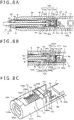
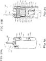
- FIGS. 19A and 19B show a conventional example of construction of a variable capacitance capacitor type pen pressure detecting module that changes the capacitance of a capacitor forming a resonance circuit of a position indicator according to pen pressure.
- the conventional example is described in Document JP 2011-186803 .
- FIG. 19A is a general perspective view of the variable capacitance capacitor forming the pen pressure detecting module.
- FIG. 19B is a sectional view taken along line Z-Z of FIG. 19A , and is a longitudinal sectional view of the variable capacitance capacitor.
- the variable capacitance capacitor 100 in the example of FIGS. 19A and 19B changes in capacitance according to pressure (pen pressure) applied to a core body 101 (see alternate long and short dashed lines in FIG. 19B ) of the position indicator.
- the position indicator detects the pen pressure applied to the core body 101 on the basis of the change in the capacitance of the variable capacitance capacitor, and transmits the detected pen pressure to a position detecting device.
- variable capacitance capacitor 100 includes a dielectric 103, a terminal member 104, a retaining member 105, a conductive member 106, and an elastic member 107 within a cylindrical holder 102 made of a resin, for example.
- the dielectric 103 for example has substantially a disk shape.
- the dielectric 103 has a substantially circular first surface portion 103a and a substantially circular second surface portion 103b opposed to the first surface portion 103a so as to be substantially parallel to the first surface portion 103a.
- the first surface portion 103a and the second surface portion 103b are both formed in a planar shape.
- the dielectric 103 is mounted on a flange portion 102a of the holder 102 with the second surface portion 103b faced toward another end side in an axial direction of the holder 102 on which end side the core body 101 is present.
- the terminal member 104 is formed of a conductive metal.
- the terminal member 104 has a flat portion 104a as an example of a surface portion engaged with the first surface portion 103a of the dielectric 103, two locking portions 104b and 104c formed so as to be continuous from the flat portion 104a, and a lead piece 104d similarly formed so as to be continuous from the flat portion 104a.
- the two locking portions 104b and 104c have substantially the shape of a letter J, and are provided so as to sandwich the flat portion 104a therebetween.
- the two locking portions 104b and 104c provide elasticity to the terminal member 104 so that the flat portion 104a of the terminal member 104 is always biased elastically in directions toward end portions of the locking portions 104b and 104c.
- the end portions of the locking portions 104b and 104c are provided with opening portions 104e and 104f having substantially a quadrangular shape, for example.
- the terminal member 104 is fixed to the holder 102, with the opening portions 104e and 104f of the two locking portions 104b and 104c locked to locking tooth portions 102b and 102c of the holder 102.
- the terminal member 104 has the elasticity provided by the two locking portions 104b and 104c, the flat portion 104a abuts against the first surface portion 103a of the dielectric 103 in a state of being pressed against the first surface portion 103a.
- the flat portion 104a of the terminal member 104 has a surface shape (flat surface in the present example) corresponding to the surface shape of the first surface portion 103a of the dielectric 103.
- the flat portion 104a and the first surface portion 103a of the dielectric 103 abut against each other without any gap therebetween, and are securely connected electrically to each other.
- the lead piece 104d of the terminal member 104 is connected to a contact portion of a printed board (not shown), disposed on an opposite side from the core body 101, by resistance welding or ultrasonic welding, for example.
- the terminal member 104 is thereby connected electrically to electronic parts on the printed board.
- the lead piece 104d of the terminal member 104 forms a first electrode of the variable capacitance capacitor 100.
- the retaining member 105 has a base portion 105a having an outside diameter slightly smaller than the inside diameter of a hollow portion of the holder 102 and a substantially cylindrical fitting portion 105b.
- An engaging recessed portion 105c (see FIG. 19B ) recessed in substantially a cylindrical shape is provided in the base portion 105a.
- An end portion in the axial direction of the core body 101 is press-fitted into the engaging recessed portion 105c, whereby the core body 101 is coupled to the retaining member 105.
- the fitting portion 105b as a recessed portion for attaching the conductive member 106 is formed in the retaining member 105 so as to project to an opposite side from the core body 101 side of the base portion 105a.
- the conductive member 106 is fitted into the fitting portion 105b.
- the conductive member 106 is formed in the form of a shell, for example, and has a curved surface portion 106a at one end in the axial direction of the conductive member 106.
- a cylindrical portion 106b on another end side in the axial direction of the conductive member 106 is fitted into the fitting portion 105b of the retaining member 105.
- the diameter of the cylindrical portion 106b of the conductive member 106 is, for example, set somewhat larger than the inside diameter of the fitting portion 105b of the retaining member 105.
- the relation of a fit between the conductive member 106 and the fitting portion 105b of the retaining member 105 is thereby set as the relation of a frictional fit. As a result, the conductive member 106 is prevented from falling off the fitting portion 105b of the retaining member 105.
- the conductive member 106 has conductivity, and is formed of an elastic member capable of elastic deformation.
- an elastic member includes for example a silicon conductive rubber, a pressure conductive rubber (PCR: Pressure sensitive Conductive Rubber), and the like.
- PCR Pressure sensitive Conductive Rubber
- a contact area between the second surface portion 103b of the dielectric 103 and the curved surface portion 106a of the conductive member 106 is increased with an increase in pen pressure (pressure) applied to the core body 101.
- the elastic member 107 is for example a coil spring having conductivity.
- the elastic member 107 has a winding portion 107a having elasticity, a terminal piece 107b at one end portion of the winding portion 107a, and a connecting portion 107c at another end portion of the winding portion 107a.
- the winding portion 107a of the elastic member 107 is disposed so as to cover the periphery of the conductive member 106 with the fitting portion 105b of the retaining member 105 interposed therebetween.
- the connecting portion 107c of the elastic member 107 is interposed between the retaining member 105 and the conductive member 106, and comes into contact with the conductive member 106.
- the elastic member 107 is thereby electrically connected to the conductive member 106.
- the terminal piece 107b of the elastic member 107 projects to one end side in the axial direction of the holder 102 through a through hole (not shown) provided in the holder 102.
- the terminal piece 107b is connected to a contact portion (not shown) of the printed board by soldering, resistance welding, or ultrasonic welding, for example.
- the terminal piece 107b of the elastic member 107 forms a second electrode of the variable capacitance capacitor 100.
- Two engaging projecting portions 105d and 105e having a substantially triangular sectional shape are provided on two flat surface portions opposed to each other in side surface portions of the base portion 105a of the retaining member 105.
- Engaging holes 102d and 102e with which the engaging projecting portions 105d and 105e of the retaining member 105 are engaged are formed in the holder 102.
- the retaining member 105 is press-fitted into the holder 102 so that the two engaging projecting portions 105d and 105e are engaged with the two engaging holes 102d and 102e provided in the holder 102.
- the elastic member 107 is retained between the flange portion 102a of the holder 102 and the base portion 105a, and the retaining member 105 is retained in the holder 102 in a state of being movable along the axial direction of the holder 102 by the length of the engaging holes 102d and 102e in the axial direction of the holder 102.
- the curved surface portion 106a formed on one end side in the axial direction of the conductive member 106 is disposed so as to be opposed to the second surface portion 103b of the dielectric 103, and the conductive member 106 forms the second electrode portion of the variable capacitance capacitor 100.
- variable capacitance capacitor 100 formed as described above in a state in which no pressure (pen pressure) is applied to the core body 101 (initial state), the conductive member 106 is physically separated from the second surface portion 103b of the dielectric 103, and is not in contact with the second surface portion 103b.
- pen pressure pen pressure
- the thickness of an air layer between the conductive member 106 and the second surface portion 103b of the dielectric 103 becomes smaller than in the initial state.
- the curved surface portion 106a of the conductive member 106 comes into contact with the second surface portion 103b of the dielectric 103.
- the contact area between the second surface portion 103b of the dielectric 103 and the curved surface portion 106a of the conductive member 106 corresponds to the pressure applied to the core body 101.
- the state between the first electrode and the second electrode of the variable capacitance capacitor 100 changes as described above according to the pressing force applied to the core body 101.
- the capacitance of a capacitor formed between the first electrode and the second electrode changes according to the pressing force applied to the core body 101.
- the above-described example is an example of a variable capacitance capacitor type pen pressure detecting module.
- a plurality of parts are arranged in the axial direction of a core body of a position indicator (see Document JP 2002-244806 for example).
- the casing of the position indicator plays a role of a holder for housing the plurality of parts of the pen pressure detecting module.
- Document US 7 202 862 B1 discloses a pressure sensor in a digitizer pen comprising a first sensor section that has a non-carbon ink disclosed thereon and a second sensor section that has a resistive, non-carbon ink disposed thereon.
- the second sensor section abuts the first sensor section.
- the digitizer pen comprises a barrel in which a pressure sensor is accommodated.
- the barrel comprises a front and a rear housing, wherein an inside holder is fixedly mounted inside the front housing.
- the pen pressure detecting module has the plurality of parts arranged within the hollow holder in the axial direction of the core body of the position indicator.
- the portion of the pen pressure detecting module is conventionally manufactured by inserting and arranging all of the plurality of parts of the pen pressure detecting module into the hollow portion of the cylindrical holder from one opening and another opening in the axial direction of the holder.
- the pen pressure detecting module is formed as one module part by housing the plurality of parts in the holder separate from the casing of the position indicator as in the above-described example, the manufacturing of the module part takes much time, so that the module part is not suitable for mass production, as described above, and cost is increased.
- a position indicator is provided that can solve the above problems.
- the position indicator includes a cylindrical casing; a core body disposed within the casing such that a tip of the core body projects from one opening end side of the casing; a printed board disposed within the casing, a circuit element being disposed on the printed board for detecting pressing force applied to the tip of the core body; and a pen pressure detecting module formed by arranging a plurality of parts for detecting a displacement of the core body in an axial direction of the casing, the displacement corresponding to the pressing force applied to the tip, in the axial direction within a hollow portion of a cylindrical holder portion housed within a hollow portion of the casing such that an axial direction of the cylindrical holder portion coincides with the axial direction of the casing; wherein the holder portion has an opening portion in a portion of a side circumferential surface of the holder portion, the opening portion being opened in a direction perpendicular to the
- the at least one of the plurality of parts forming the pen pressure detecting module is (are) housed through the opening portion formed in a portion of the side circumferential surface of the cylindrical holder portion and opened in the direction perpendicular to the axial direction of the holder portion.
- the at least one of the plurality of parts housed in the holder portion may fall out through the opening portion.
- the holder portion has the locking portion for preventing the at least one of the plurality of housed parts from falling out through the opening portion, so that the plurality of housed parts will be retained in the holder portion.
- the plurality of parts forming the pen pressure detecting module include one or more first parts displaced in the axial direction of the casing according to the pressing force applied to the tip of the core body and a second part for always biasing at least one of the first parts toward a side of the tip of the core body.
- the at least one of the first parts is moved in the axial direction and engaged with the locking portion of the holder portion by a biasing force of the second part within the hollow portion of the holder portion, whereby the locking portion of the holder portion prevents the plurality of parts from falling out through the opening portion.
- the plurality of parts forming the pen pressure detecting module include one or more first parts displaced in the axial direction of the casing according to the pressing force applied to the tip of the core body, and the second part for always biasing at least one of the first parts toward the side of the tip of the core body.
- the plurality of parts forming the pen pressure detecting module are housed via the opening portion opened in the direction perpendicular to the axial direction of the holder portion, the second part moves the at least one of the first parts in the axial direction by the elastic biasing force of the second part.
- the locking portion is engaged with the at least one of the first parts moved in the axial direction.
- the second part applies the elastic biasing force in the axial direction to the plurality of parts as a whole, when the at least one of the first parts is engaged with the locking portion and is prevented from falling out through the opening portion, the plurality of parts as a whole are prevented from falling out through the opening portion.
- the locking portion of the holder portion includes a pair of edge portions of the opening portion along the axial direction, which are opposed to each other.
- the pair of edge portions is elastically displaced such that at least one of the plurality of parts increases a distance between the pair of edge portions when the plurality of parts are housed (inserted) into the cylindrical holder portion in the direction perpendicular to the axial direction through the opening portion, and the distance between the pair of edge portions is elastically restored to an original state when the plurality of parts are housed within the cylindrical holder portion, whereby the locking portion of the holder portion prevents the plurality of parts from falling out through the opening portion.
- the locking portion of the holder portion includes the pair of edge portions of the opening portion along the axial direction, which are opposed to each other.
- the pair of edge portions is elastically displaced such that at least a part of the plurality of parts increases the distance between the pair of edge portions.
- the pair of edge portions forming the locking portion elastically restores the distance therebetween to an original state. The plurality of parts are thereby prevented from being displaced thorough the opening portion of the holder portion.
- At least one of the plurality of parts for pen pressure detection is/are housed into the hollow portion of the holder portion via the opening portion opened in the direction perpendicular to the axial direction of the holder portion in a portion of the side circumferential surface of the cylindrical holder portion.
- the locking portion of the holder portion prevents the plurality of housed parts from falling out through the opening portion.
- the housed state of the plurality of parts within the cylindrical holder portion can be monitored and visually verified through the opening portion.
- the positional relation of the plurality of parts forming the pen pressure detecting module within the holder portion can be maintained to be a predetermined positional relation at all times.
- FIGS. 1A to 4C are diagrams of assistance in explaining an example of construction of a first embodiment of the position indicator according to the present invention.
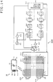
- FIG. 2 shows an example of an electronic device 200 using the position indicator 1 according to the first embodiment.
- the electronic device 200 is a high-functionality portable telephone terminal having a display screen 200D of a display device, such as an LCD (Liquid Crystal Display), and includes a position detecting device 202 of an electromagnetic induction system under (on the back side of) the display screen 200D.
- a display screen 200D of a display device such as an LCD (Liquid Crystal Display)
- a position detecting device 202 of an electromagnetic induction system under (on the back side of) the display screen 200D.
- a casing of the electronic device 200 in the present example has a housing recessed hole 201 for housing the position indicator 1 in the shape of a pen.
- a user extracts the position indicator 1 housed in the housing recessed hole 201 from the electronic device 200, and performs position indicating operation on the display screen 200D, as required.
- the position detecting device 202 When position indicating operation is performed on the display screen 200D of the electronic device 200 by the position indicator 1 in the shape of a pen, the position detecting device 202 provided on the back side of the display screen 200D detects the position operated (acted on) by the position indicator 1 and pen pressure, and a microcomputer included in the position detecting device 202 of the electronic device 200 performs display processing corresponding to the operated position on the display screen 200D and the pen pressure.
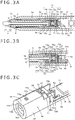
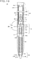
- FIGS. 1A and 1B schematically show the position indicator 1 as a whole according to the first embodiment.
- FIG. 1A shows the inside of a case main body 2a of a case 2 (casing) of the position indicator 1 with only the case main body 2a cut away for purposes of illustration.
- FIG. 1B is a view of the position indicator 1 according to the first embodiment as viewed in an axial direction from the side of a core body 4.
- the position indicator 1 has the case 2 forming a bottomed cylindrical casing that is long and thin in the axial direction and which is closed on one side.
- the case 2 is formed of a resin, for example, and includes the case main body 2a of a cylindrical shape having a hollow portion therewithin and a case cap 2b coupled to the case main body 2a.
- the core body 4 and a magnetic core wound with a coil 5, or a ferrite core 6 in the present example, are coupled to and housed in a board holder 3 within the hollow portion of the case main body 2a.
- the ferrite core 6 in the present example has a cylindrical shape.
- the board holder 3 is formed of a resin, for example, and is formed so as to have a pressure sensing part holder portion 3a and a printed board mounting base portion 3b continuous with each other in a longitudinal direction as the axial direction of the position indicator 1 when the board holder 3 is housed within the hollow portion of the case main body 2a.
- Pressure sensing parts (a plurality of parts for pen pressure detection) 7 are housed in the pressure sensing part holder portion 3a.
- a printed board 8 is mounted and retained on the printed board mounting base portion 3b.
- the pressure sensing part holder portion 3a will hereinafter be abbreviated to the holder portion 3a for the simplicity of description.
- the holder portion 3a is formed closest to the core body 4 in the board holder 3.
- the core body 4 and the ferrite core 6 are coupled to the holder portion 3a.
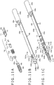
- FIG. 3A is a sectional view taken along line X-X of FIG. 1B , and is a partial sectional view of the position indicator 1 sectioned in a direction passing through the axial position of the position indicator 1 and parallel with a board surface (surface on which a conductor pattern is printed and formed and circuit parts are mounted) 8a of the printed board 8.
- FIG. 3B is a sectional view taken along line Y-Y of FIG. 1B , and is a partial sectional view of the position indicator 1 sectioned in a direction passing through the axial position of the position indicator 1 and perpendicular to the board surface 8a of the printed board 8.
- FIG. 3C is a perspective view directing attention to the holder portion 3a, in particular, of the board holder 3.
- FIG. 4B is a diagram showing a state in which the core body 4 and the ferrite core 6 are coupled to the board holder 3.
- FIG. 4A is an exploded perspective view of assistance in explaining the holder portion 3a of the board holder 3 and the pressure sensing parts 7.
- FIG. 4C is a sectional view taken along line A-A of FIG. 4A , and is a longitudinal sectional view of the holder portion 3a of the board holder 3.
- the printed board 8 is mounted on the printed board mounting base portion 3b of the board holder 3.
- the printed board 8 is of a long and thin rectangular shape having a width smaller than the inside diameter of the case main body 2a and having a predetermined length in the longitudinal direction.
- the length in the longitudinal direction of a board mounting flat surface of the printed board mounting base portion 3b is substantially equal to or slightly larger than the length in the longitudinal direction of the printed board 8.
- the length in a width direction of the board mounting flat surface of the printed board mounting base portion 3b is selected to be slightly larger than the width of the printed board 8.
- one end and the other end of the coil 5 extend to the printed board 8 using a clearance between the board holder 3 and the case main body 2a, and are for example soldered to a conductive pattern formed on the printed board 8.
- a notch portion 31 is formed in a portion in the longitudinal direction of the board holder 3, and the one end and the other end of the coil 5 are soldered on a back surface side opposite from the board surface 8a of the printed board 8 and are connected to the conductive pattern on the printed board 8 via a through hole.
- the printed board 8 is provided with a push switch (side switch) 11 that is turned on when depressed and which returns to an off state when the depression is stopped, and is provided with capacitors 12 and 13 forming a resonance circuit together with the coil 5.
- the capacitor 12 in the present example is a trimmer capacitor whose capacitance can be adjusted.
- an IC 14 is provided on the printed board 8, and other circuit parts and a conductor pattern not shown in the figures are formed on the printed board 8.
- a through hole 15 (see FIG. 2 ) is made at a position of a side circumferential surface of the case main body 2a of the position indicator 1 which position corresponds to the side switch 11.
- a depression operating element 16 of the side switch 11 is exposed such that the side switch 11 can be depressed through the through hole 15.
- a predetermined function is assigned and set to the operation of depressing the side switch 11 by the depression operating element 16 on the side of the electronic device 200 including the position detecting device 202.
- the electronic device 200 in the present example can assign and set the operation of depressing the side switch 11 by the depression operating element 16 as an operation similar to a click operation on a pointing device such as a mouse or the like.
- the capacitors 12 and 13 forming a portion of the resonance circuit and the IC 14 in the present example are disposed as chip parts on the printed board 8.
- the resonance frequency of the resonance circuit is adjusted by adjusting the capacitance of the trimmer capacitor 12.
- locking portions 32 and 33 for locking the printed board 8 to the printed board mounting base portion 3b by sandwiching the printed board 8 in a direction of thickness thereof at both end portions in the longitudinal direction of the printed board 8 are formed at both end portions in the longitudinal direction of the printed board mounting base portion 3b of the board holder 3.
- the printed board 8 in a state of being mounted on the printed board mounting base portion 3b and locked by the locking portions 32 and 33 is not in contact with an inner wall surface of the case main body 2a but is separated from the case main body 2a.
- the pressure sensing parts 7 formed by a plurality of parts as shown in FIG. 1A , FIGS. 3A to 3C , and FIG. 4A are housed in the holder portion 3a of the board holder 3.
- a pen pressure detecting module is formed by thus housing the pressure sensing parts 7 in the holder portion 3a.
- a core body main body 42 of the core body 4 is coupled to the pen pressure detecting module, whereby the pressure sensing parts 7 of the pen pressure detecting module detect pen pressure applied to a projecting member 41 of the core body 4. Construction of the pressure sensing parts 7 of the pen pressure detecting module and the housing of the pressure sensing parts 7 in the holder portion 3a will be described later in detail.
- the board holder 3 has a flat surface 3pn (see FIG.
- the flat surface 3pn is a flush flat surface along the axial direction on the holder portion 3a or from the holder portion 3a to the printed board mounting base portion 3b.
- the board holder 3 is mounted on a predetermined flat surface of a workbench in a stable state without rolling because of the flat surface 3pn.
- the opening portion 35 of the holder portion 3a is an opening in a direction orthogonal to the predetermined flat surface of the workbench
- the printed board mounting flat surface of the printed board mounting base portion 3b is a surface parallel to the predetermined flat surface of the workbench.
- the work of housing the pressure sensing parts 7 in the holder portion 3a of the board holder 3 mounted on the flat surface of the workbench through the opening portion 35 can be surely performed, and the printed board 8 can be surely mounted and locked on the mounting flat surface of the printed board mounting base portion 3b.
- the board holder 3 is coupled to the case cap 2b at the coupling portion 3c at an end portion of the printed board mounting base portion 3b, which end portion is on the opposite side from the holder portion 3a in the longitudinal direction, so that the case cap 2b and the board holder 3 can be handled as an integral object.
- an object formed by mounting and fixing the printed board 8 on the printed board mounting base portion 3b of the board holder 3, housing the pressure sensing parts 7 in the holder portion 3a, and coupling the ferrite core 6 wound with the coil 5 and the core body 4 to the board holder 3 can be handled as one module part.
- the module part is housed within the hollow portion of the case main body 2a, whereby the position indicator 1 is completed.
- the board holder 3 is coupled to the case cap 2b so as to be locked to the inside of the case main body 2a in such a state that the position of a center line in the axial direction of the holder portion 3a coincides with the position of a center line in the axial direction of the cylindrical case main body 2a.
- one end side in the axial direction of the case main body 2a is a pen point side of the position indicator 1 in the shape of a pen, and a through hole 21 (opening) is provided on the pen point side of the case main body 2a.
- the core body 4 in the present example is formed by the projecting member (pen point member) 41 projecting from the through hole 21 of the case main body 2a to the outside and the core body main body 42.
- the core body 4 is made of a synthetic resin such as a polyacetal resin (Duracon) or the like in consideration of resistance to friction when the projecting member 41 is used in a state of abutting against the operating surface.
- the core body main body 42 is a cylindrical rod-shaped body having a smaller diameter than the diameter of the projecting member 41.
- a through hole 6a having a larger inside diameter than the diameter of the core body main body 42 is formed in the ferrite core 6 in the axial direction of the ferrite core 6.
- the core body main body 42 of the core body 4 is inserted through the through hole 6a of the ferrite core 6 to be coupled to one of the plurality of parts forming the pressure sensing parts 7, as will be described later.
- one end side (side opposite from the side of the projecting member 41 of the core body 4) in the axial direction of the ferrite core 6 is coupled to the holder portion 3a of the board holder 3 via an anti-falling member 9 formed of an elastic material, for example a silicon rubber in the present example.
- an elastic material for example a silicon rubber in the present example.
- the pen pressure detecting module in the present example uses a variable capacitance capacitor whose capacitance varies according to pen pressure applied to the core body as with the pen pressure detecting module described at the beginning with reference to Document JP 2011-186803 .
- the pressure sensing parts 7 in the present example are formed by a plurality of parts, that is, a dielectric 71, a terminal member 72, a retaining member 73, a conductive member 74, and an elastic member 75.
- the terminal member 72 forms a first electrode of the variable capacitance capacitor formed by the pressure sensing parts 7.
- the conductive member 74 and the elastic member 75 are electrically connected to each other to form a second electrode of the variable capacitance capacitor.
- the holder portion 3a of the board holder 3 is formed by the cylindrical body 34 having a hollow portion, and is formed so as to house the pressure sensing parts 7 arranged in the axial direction within the hollow portion of the cylindrical body 34.
- the dielectric 71 and the terminal member 72 which are parts not moving in the axial direction within the holder portion 3a formed by the cylindrical body 34, are inserted in the direction orthogonal to the axial direction of the cylindrical body 34 and perpendicular to the board surface 8a of the printed board 8, through the opening portion 35 formed in a portion of the side circumferential surface of the cylindrical body 34 forming the holder portion 3a and opened in the direction orthogonal to the axial direction, as shown in FIG. 4A , and are housed as shown in FIG. 3C and FIG. 4B .
- the opening portion 35 is formed in an end portion of the side circumferential surface of the cylindrical body 34 forming the holder portion 3a, which end portion is on the side of the printed board mounting base portion 3b.
- the opening portion 35 is opened in the direction orthogonal to the axial direction and opened in the direction perpendicular to the board surface 8a of the printed board 8 mounted on the printed board mounting base portion 3b.
- the opening portion 35 has a predetermined length d1 (see FIG. 4C ) in the axial direction, and has a predetermined length d2 (not shown) in the direction orthogonal to the axial direction.
- the length d1 is selected to be larger than the length (thickness) in the axial direction of the dielectric 71 and the terminal member 72 when the dielectric 71 and the terminal member 72 are superposed on each other in the axial direction.
- the length d2 is selected to be slightly larger than the larger length of the lengths of the dielectric 71 and the terminal member 72 in the direction orthogonal to the axial direction.
- the cylindrical body 34 forming the holder portion 3a has an inside diameter d3 (see FIG. 4C ), and has an opening 36a on the side of the core body 4 in the axial direction of the cylindrical body 34.
- a portion 36 having the opening 36a on the side of the core body 4 in the axial direction does not have an opening in the side circumferential surface.
- the length d2 in the direction orthogonal to the axial direction of the opening portion 35 in the side circumferential surface of the cylindrical body 34 is selected to be equal to the inside diameter d3 of the cylindrical body 34, but is selected to be larger by the depth of a recessed groove 39, to be described later, in the portion of the recessed groove 39.
- the cylindrical body 34 forming the holder portion 3a is closed by a wall portion 37 on the side of the printed board mounting base portion 3b.
- the locking portion 32 described above is formed on the wall portion 37 so as to project on the side of the printed board mounting base portion 3b.
- the opening portion 35 is formed so as to expose the wall portion 37 to the outside. That is, the opening portion 35 is made in the side circumferential surface of the cylindrical body 34 so as to form an opening of the length d1 from the wall portion 37 in the axial direction.
- Slits 38a and 38b having a predetermined width slightly larger than the thickness of the terminal member 72 in the axial direction are formed in a coupling portion of the side circumferential surface of the cylindrical body 34, which coupling portion is coupled to the wall portion 37.
- the recessed groove 39 (see FIG. 3A and FIG. 4C ) having a larger inside diameter than the inside diameter d2 of the portion of the cylindrical body 34, in which portion the opening portion 35 is formed, is formed at a position adjacent to the slits 38a and 38b in the axial direction in the inner wall of the cylindrical body 34.
- the dielectric 71 is formed as a plate-shaped object having an external shape to be fitted into the recessed groove 39 and having a thickness corresponding to the width in the axial direction of the recessed groove 39. Therefore, the dielectric 71 can be inserted and fitted into the recessed groove 39 of the cylindrical body 34 through the opening portion 35, and the recessed groove 39 prevents the dielectric 71 in the fitted state from moving in the axial direction within the cylindrical body 34.
- the dielectric 71 is pressed and biased by the conductive member 74, and is thus pressed to the side of the wall portion 37. Therefore the recessed groove 39 need not be provided.
- the terminal member 72 is formed by a disk-shaped conductive member, for example a plate-shaped object of a conductive metal, which has a thickness slightly smaller than the width in the axial direction of the slits 38a and 38b of the cylindrical body 34 and has an outside diameter corresponding to the inside diameter d3 of the cylindrical body 34. As shown in FIG. 4A , the terminal member 72 has bulging portions 72a and 72b to be fitted into the slits 38a and 38b of the cylindrical body 34.
- the terminal member 72 can be inserted so as to be in contact with the wall portion 37 of the cylindrical body 34 through the opening portion 35, and the bulging portions 72a and 72b are fitted into the slits 38a and 38b of the cylindrical body 34 by the insertion and locked to the cylindrical body 34 so as not to move in the axial direction.
- a swelling portion 72c swelling toward the side of the dielectric 71 is formed on a central portion of a plate surface of the terminal member 72, which plate surface is on the side of the dielectric 71.
- the swelling portion 72c plays a role of surely bringing the dielectric 71 and the terminal member 72 into contact with each other when the dielectric 71 and the terminal member 72 are housed within the cylindrical body 34.
- the terminal member 72 plays the role of the first electrode of the variable capacitance capacitor.
- the terminal member 72 has a lead portion 72d formed from an end surface as an upper end of the terminal member 72, which upper end is on the side of the opening portion 35.
- the lead portion 72d straddles the wall portion 37 of the cylindrical body 34 to be connected by soldering to a land portion 8b (see FIG. 3C ) on the board surface 8a of the printed board 8 mounted on the printed board mounting base portion 3b when the terminal member 72 is housed within the holder portion 3a.
- the terminal member 72 has an L-shaped projection 72e formed in substantially the center of the end surface as the upper end of the terminal member 72, which upper end is on the side of the opening portion 35.
- the L-shaped projection 72e projects on an opposite side from the lead portion 72d when the terminal member 72 is housed within the holder portion 3a.
- the L-shaped projection 72e of the terminal member 72 holds down the opening side end portion of the dielectric 71 when the dielectric 71 and the terminal member 72 are housed within the holder portion 3a.
- the retaining member 73 has a cylindrical shape portion 73a having a recessed hole 73b, into which to press-fit the core body main body 42 of the core body 4 on the core body 4 side in the axial direction of the retaining member 73.
- the retaining member 73 also has a ring-shaped projecting portion 73c having a recessed hole 73d, into which to fit the conductive member 74 on an opposite side in the axial direction from the side of the recessed hole 73b.
- the recessed hole 73b and the recessed hole 73d are formed such that the center line (axial position) of the recessed hole 73b and the center line (axial position) of the recessed hole 73d are located on one straight line.
- the outside diameter (portion in a circumferential direction) of the cylindrical shape portion 73a of the retaining member 73 is selected to be slightly smaller than the inside diameter d3 of the cylindrical body 34.
- the outside diameter of the ring-shaped projecting portion 73c of the retaining member 73 is selected to be smaller than the outside diameter of the cylindrical shape portion 73a and smaller than the inside diameter of a coil spring forming the elastic member 75 to be described later.
- a stepped portion is formed between the ring-shaped projecting portion 73c and the cylindrical shape portion 73a. The stepped portion is to lock an end portion of the spring as the elastic member 75 to be described later.
- slits 73e and 73f are formed in the cylindrical shape portion 73a and the ring-shaped projecting portion 73c so as to traverse the recessed hole 73b and the recessed hole 73d, respectively.
- the presence of the slits 73e and 73f allows the cylindrical shape portion 73a and the ring-shaped projecting portion 73c to be elastically displaced (deformed) in the direction orthogonal to the axial direction.
- Engaging projecting portions 73g and 73h are formed on the side circumferential surface of the cylindrical shape portion 73a of the retaining member 73 at such positions as to be opposed to each other, while interposing the axial center position of the cylindrical shape portion 73a therebetween.
- Engaging holes 34a and 34b (see FIG. 3B and FIG. 4C ), into which to engage the engaging projecting portions 73g and 73h formed on the side circumferential surface of the cylindrical shape portion 73a of the retaining member 73, are formed in the side circumferential surface of the cylindrical body 34 forming the holder portion 3a.
- the length d4 (see FIG. 4C ) in the axial direction of the engaging holes 34a and 34b is larger than the length in the axial direction of the engaging projecting portions 73g and 73h formed on the side circumferential surface of the cylindrical shape portion 73a of the retaining member 73.
- the length d4 is selected to be a value such that the conductive member 74 can be moved in the axial direction and abut against the dielectric 71 and be further elastically deformed in a state in which all of the pressure sensing parts 7 are housed within the hollow portion of the cylindrical body 34.
- the conductive member 74 is made of a conductive and elastically deformable elastic member, and is for example formed by a silicon conductive rubber or a pressure conductive rubber.
- the conductive member 74 includes a large-diameter portion 74a formed by a cylindrical portion having an outside diameter equal to the outside diameter of the ring-shaped projecting portion 73c of the retaining member 73 and a small-diameter portion 74b formed by a cylindrical portion having an outside diameter substantially equal to the diameter of the recessed hole 73d of the ring-shaped projecting portion 73c.
- the positions of center lines of the large-diameter portion 74a and the small-diameter portion 74b are the same. As shown in FIGS.
- an end surface of the large-diameter portion 74a which end surface is on an opposite side from the small-diameter portion 74b, is formed so as to have a curved surface portion swelling in the form of a shell.
- the height of the small-diameter portion 74b of the conductive member 74 is selected to be substantially equal to the depth of the recessed hole 73d formed in the ring-shaped projecting portion 73c of the retaining member 73.
- the elastic member 75 is for example formed by a coil spring having conductivity.
- the elastic member 75 has a winding portion 75a having elasticity, a terminal piece 75b at one end portion of the winding portion 75a, and a connecting portion 75c at another end portion of the winding portion 75a.
- the winding portion 75a of the coil spring forming the elastic member 75 has a diameter that allows the conductive member 74 to be housed within the winding portion 75a without the winding portion 75a being in contact with the conductive member 74, and which diameter is smaller than the diameter of the cylindrical shape portion 73a of the retaining member 73.
- the connecting portion 75c of the elastic member 75 is inserted from the slit portion of the ring-shaped projecting portion 73c of the retaining member 73 into the bottom of the recessed hole 73d formed in the ring-shaped projecting portion 73c (see FIG. 3A and FIG. 3B ).
- the small-diameter portion 74b of the conductive member 74 is press-fitted into the ring-shaped projecting portion 73c of the retaining member 73, the end surface of the small-diameter portion 74b of the conductive member 74 is brought into contact with the connecting portion 75c of the elastic member 75 having conductivity, and is thus electrically connected to the connecting portion 75c.
- the terminal piece 75b of the elastic member 75 straddles the dielectric 71, the terminal member 72, and the wall portion 37, and is connected by soldering to the conductive pattern on the board surface 8a of the printed board 8 mounted on the printed board mounting base portion 3b.
- the board holder 3 is mounted on the flat surface of the workbench such that the flat surface 3pn faces the flat surface of the workbench.
- the board holder 3 is positioned such that the opening of the opening portion 35 faces in an upward direction orthogonal to the flat surface of the workbench and the printed board mounting flat surface of the printed board mounting base portion 3b is parallel to the flat surface of the workbench, and the board holder 3 is locked on the flat surface of the workbench.
- the dielectric 71 and the terminal member 72 of the pressure sensing parts 7 are housed within the hollow portion of the cylindrical body 34 forming the holder portion 3a through the opening portion 35.
- the dielectric 71 and the terminal member 72 are housed within the hollow portion of the cylindrical body 34 in a state in which the L-shaped projection 72e of the terminal member 72 holds down the opening side end portion of the dielectric 71 housed within the hollow portion of the cylindrical body 34.
- the dielectric 71 is housed within the recessed groove 39 formed in the inner wall of the cylindrical body 34, and the bulging portions 72a and 72b of the terminal member 72 are fitted into the slits 38a and 38b of the holder portion 3a.
- the small-diameter portion 74b of the conductive member 74 is press-fitted into the recessed hole 73d of the ring-shaped projecting portion 73c of the retaining member 73, and the winding portion 75a of the elastic member 75 is arranged so as to be brought around the periphery of the ring-shaped projecting portion 73c and the conductive member 74.
- the connecting portion 75c of the elastic member 75 is sandwiched between the upper end surface of the small-diameter portion 74b of the conductive member 74 and the bottom of the recessed hole 73d of the ring-shaped projecting portion 73c, so that the connecting portion 75c of the elastic member 75 and the conductive member 74 are electrically connected to each other.
- the combination of the retaining member 73, the conductive member 74, and the coil spring of the elastic member 75 is inserted in the axial direction into the hollow portion of the cylindrical body 34 from the side of the conductive member 74 through the opening 36a of the cylindrical body 34. Then, the combination of the retaining member 73, the conductive member 74, and the coil spring of the elastic member 75 is inserted in the axial direction until the engaging projecting portions 73g and 73h formed on the cylindrical shape portion 73a of the retaining member 73 are fitted into the engaging holes 34a and 34b formed in the side circumferential surface of the cylindrical body 34.
- the cylindrical shape portion 73a of the retaining member 73 is elastically deformed in the direction orthogonal to the axial direction and inserted into the hollow portion of the cylindrical body 34 in spite of the presence of the engaging projecting portions 73g and 73h because the slit 73e is formed.
- the retaining member 73 When the engaging projecting portions 73g and 73h formed on the cylindrical shape portion 73a of the retaining member 73 are fitted into the engaging holes 34a and 34b formed in the side circumferential surface of the cylindrical body 34 of the holder portion 3a, the retaining member 73 is locked to the inside of the hollow portion of the cylindrical body 34 of the holder portion 3a. Thus, the retaining member 73 will not fall out through the opening 36a of the cylindrical body 34 of the holder portion 3a irrespective of a biasing force in the axial direction of the elastic member 75. In addition, in this state, the dielectric 71 and the terminal member 72 are pressed to the side of the wall portion 37 by the biasing force in the axial direction of the elastic member 75. This prevents the dielectric 71 and the terminal member 72 from falling out through the opening portion 35 of the cylindrical body 34.
- locking mechanism for preventing the dielectric 71 and the terminal member 72 forming parts of the pressure sensing parts 7 from being displaced in the direction orthogonal to the axial direction is formed by the engagement between the engaging holes 34a and 34b formed in the cylindrical body 34 and the engaging projecting portions 73g and 73h of the cylindrical shape portion 73a of the retaining member 73 and the biasing force of the elastic member 75.
- the lead portion 72d of the terminal member 72 is soldered to the land portion 8b of the printed board 8, and the terminal piece 75b of the coil spring as the elastic member 75 is soldered to the printed board 8.
- the soldering and fixing of the lead portion 72d of the terminal member 72 and the terminal piece 75b of the elastic member 75 to the printed board 8 can more surely prevent the terminal member 72 from falling out through the opening portion 35 of the holder portion 3a.
- the L-shaped projection 72e of the terminal member 72 holds down the opening side end portion of the dielectric 71 housed within the hollow portion of the cylindrical body 34 of the holder portion 3a. Therefore the soldering and fixing of the terminal member 72 to the printed board 8 can more surely prevent the dielectric 71 from falling out through the opening portion 35 of the cylindrical body 34 of the holder portion 3a.
- the retaining member 73 fitted with the conductive member 74 is prevented from moving to the side of the core body 4 in the axial direction with the engaging projecting portions 73g and 73h engaged with the engaging holes 34a and 34b of the cylindrical body 34, but is movable to the side of the dielectric 71 in the axial direction within the hollow portion of the cylindrical body 34.
- the biasing force of the elastic member 75 creates an air space between the conductive member 74 and the dielectric 71.
- the anti-falling member 9 is press-fitted into the opening 36a of the cylindrical body 34, as shown in FIGS. 3A and 3B and FIG. 4B .
- the anti-falling member 9 has a through hole 9a into which to insert the core body main body 42 of the core body 4 in the axial direction, and has a cylindrical portion 9b having an outside diameter substantially equal to or slightly smaller than the inside diameter of the portion 36 on the side of the opening 36a of the cylindrical body 34.
- the anti-falling member 9 is coupled to the holder portion 3a by press-fitting the cylindrical portion 9b of the anti-falling member 9 into the portion 36 on the side of the opening 36a of the cylindrical body 34.
- the anti-falling member 9 has a recessed portion 9c having an inside diameter substantially equal to the outside diameter of the ferrite core 6 on an opposite side from the cylindrical portion 9b in the axial direction.
- the ferrite core 6 is coupled to the holder portion 3a of the board holder 3 via the anti-falling member 9 by press-fitting an end portion of the ferrite core 6, which end portion is on an opposite side from the side of the projecting member 41 of the core body 4, into the recessed portion 9c of the anti-falling member 9.
- the anti-falling member 9 is formed of a material having elasticity, for example a silicon rubber.
- the ferrite core 6 is coupled to the holder portion 3a of the board holder 3 via the anti-falling member 9, the ferrite core 6 can be prevented from being damaged even if the position indicator 1 is dropped and a high acceleration is applied to the coupling portion between the ferrite core 6 and the holder portion 3a.
- the core body main body 42 of the core body 4 is inserted into the through hole 6a of the ferrite core 6. Then, an end portion of the core body main body 42 of the core body 4 is press-fitted into the recessed hole 73b of the cylindrical shape portion 73a of the retaining member 73 housed in the holder portion 3a. In this case, even in a state in which the core body 4 is press-fitted in the recessed hole 73b of the cylindrical shape portion 73a, the core body main body 42 of the core body 4 is also exposed from the ferrite core 6 to the side of the projecting member 41 of the core body 4, as shown in FIG. 3A and FIG. 4B . A pressure (pen pressure) applied to the projecting member 41 of the core body 4 can displace the core body 4 to the side of the case cap 2b in the axial direction against the biasing force of the elastic member 75.
- a pressure (pen pressure) applied to the projecting member 41 of the core body 4 can displace the core body 4 to the side of the case cap 2
- the printed board 8 is mounted on the printed board mounting base portion 3b of the board holder 3 coupled to the case cap 2b, the pressure sensing parts 7 are housed in the holder portion 3a, and the ferrite core 6 and the core body 4 are coupled to the holder portion 3a, whereby a module part as shown in FIG. 4B is formed.
- this module part is inserted into the hollow portion of the case main body 2a, so that the projecting member 41 of the core body 4 projects from the through hole 21 of the case main body 2a to the outside. Then, the case main body 2a and the case cap 2b are coupled to each other, whereby the position indicator 1 is completed.
- the core body 4 when pressure is applied to the projecting member 41 of the core body 4, the core body 4 is displaced in a direction of the inside of the case main body 2a in the axial direction according to the pressure. Then, the displacement of the core body 4 displaces the retaining member 73 within the holder portion 3a, which retaining member 73 is coupled with the core body main body 42 to the side of the dielectric 71 against the elastic biasing force of the elastic member 75.
- the conductive member 74 fitted in the retaining member 73 is displaced to the side of the dielectric 71, so that a distance between the conductive member 74 and the dielectric 71 and, further, a contact area between the conductive member 74 and the dielectric 71 change according to the pressure applied to the core body 4.
- the capacitance of the variable capacitance capacitor formed between the terminal member 72 forming the first electrode and the conductive member 74 forming the second electrode thereby changes according to the pressure applied to the core body 4.
- the change in the capacitance of the variable capacitance capacitor is transmitted from the position indicator 1 to the position detecting device 202, whereby the position detecting device 202 detects the pen pressure applied to the core body 4 of the position indicator 1.
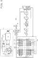
- FIG. 5 is a diagram showing an equivalent circuit of the position indicator 1 according to the first embodiment and an example of circuit configuration of the position detecting device 202 performing position detection and pen pressure detection by electromagnetic induction coupling with the position indicator 1.
- the position detecting device 202 in the example of FIG. 5 has a position detecting coil 210 formed by stacking an X-axis direction loop coil group 211 and a Y-axis direction loop coil group 212, and has a selecting circuit 213 for sequentially selecting one loop coil of the two loop coil groups 211 and 212.
- the position indicator 1 includes a signal control circuit formed by the IC 14, and is configured to obtain a driving voltage for driving the IC 14 from an exciting signal transmitted from an exciting coil 214 provided to the position detecting device 202.
- a signal control circuit formed by the IC 14, and is configured to obtain a driving voltage for driving the IC 14 from an exciting signal transmitted from an exciting coil 214 provided to the position detecting device 202.
- the loop coil groups 211 and 212 of the position detecting device 202 are used only for the reception of an electromagnetic coupling signal from the position indicator 1.
- the signal control circuit provided to the position indicator 1 is driven by the electromagnetic coupling between the loop coil groups 211 and 212 of the position detecting device 202 and the position indicator 1 in place of the exciting coil 214.
- a signal such as predetermined control data or the like is transmitted to the signal control circuit provided to the position indicator 1.
- the exciting coil 214 is disposed so as to surround the position detecting coil 210.
- the exciting coil 214 in FIG. 5 has two turns. In actuality, however, the exciting coil 214 has a larger number of turns, for example eight to ten turns.
- the exciting coil 214 is connected to a driving circuit 222.
- the driving circuit 222 is connected to an oscillating circuit 221 oscillating at a frequency fo.
- the driving circuit 222 is controlled by a processing control section 220 formed by a microcomputer.
- the processing control section 220 controls the driving circuit 222 to control the supply of an oscillating signal of the frequency fo from the oscillating circuit 221 to the exciting coil 214 and thus control signal transmission from the exciting coil 214 to the position indicator 1.
- the selecting circuit 213 selects one loop coil under selection control of the processing control section 220.
- An induced voltage generated in the loop coil selected by the selecting circuit 213 is amplified in a receiving amplifier 223, and supplied to a band-pass filter 224, so that only a component of the frequency fo is extracted.
- the band-pass filter 224 supplies the extracted component to a detecting circuit 225.
- the detecting circuit 225 detects the component of the frequency fo, and supplies a direct-current signal corresponding to the detected component of the frequency fo to a sample and hold circuit 226.
- the sample and hold circuit 226 holds a voltage value of the output signal of the detecting circuit 225 in predetermined timing, specifically predetermined timing during a receiving period, and sends out the voltage value to an A/D (analog-to-digital) converter circuit 227.
- the A/D converter circuit 227 converts the analog output of the sample and hold circuit 226 into a digital signal, and outputs the digital signal to the processing control section 220.
- the processing control section 220 supplies the signal in the predetermined timing to the sample and hold circuit 226.
- the processing control section 220 determines whether the digital signal from the A/D converter circuit 227 is a value exceeding a predetermined threshold value, and thereby determines whether the loop coil selected by the selecting circuit 213 is a loop coil at a position indicated by the position indicator 1.
- the processing control section 220 also detects the intermittence of a signal from the position indicator 1 as a digital signal of a few bits, for example 8 bits, and thereby detects pen pressure.
- the circuit configuration of the position indicator 1 is as shown enclosed by a dotted line in FIG. 5 .
- the capacitor 12 is connected in parallel with the coil 5 as an inductance element.
- the capacitor 13 and the side switch 11 are connected in series with each other.
- the series circuit of the capacitor 13 and the side switch 11 is connected in parallel with the coil 5, whereby a resonance circuit 301 is formed.
- a switch 302 is connected in parallel with the resonance circuit 301. This switch 302 is configured to be subjected to on-off control by the IC 14.
- the IC 14 is configured to operate on power Vcc obtained by rectifying an alternating-current signal received in the resonance circuit 301 by electromagnetic induction from the position detecting device 202 in a rectifying circuit (power supply circuit) 305 including a diode 303 and a capacitor 304.
- the IC 14 is connected to the resonance circuit 301 via a capacitor 306, and monitors conditions of operation of the resonance circuit 301. By monitoring the conditions of operation of the resonance circuit 301, the IC 14 can detect conditions of electromagnetic coupling to the exciting coil 214 of the position detecting device 202 or, though not described in the present example, a signal such as control data or the like transmitted from the position detecting device 202 using the two loop coil groups 211 and 212, to perform desired operation control.
- the IC 14 is further connected with the variable capacitance capacitor (capacitance Cv) formed by the pressure sensing parts 7.
- the IC 14 is configured to be able to detect the capacitance Cv corresponding to pen pressure.
- the IC 14 detects the pen pressure in the position indicator 1 from the value of the capacitance Cv.
- the IC 14 then converts the detected pen pressure into a digital signal of 8 bits, for example, and controls the switch 302 by the digital signal corresponding to the pen pressure.
- the variable capacitance capacitor formed by the pressure sensing parts 7 does not need to form the resonance circuit 301.
- the constituent elements other than the coil 5 and the variable capacitance capacitor formed by the pressure sensing parts 7 are all disposed on the printed board 8.
- the processing control section 220 first drives the driving circuit 222 to transmit a signal to the position indicator 1 from the exciting coil 214 for a predetermined time. Next, the processing control section 220 makes the selecting circuit 213 sequentially select one loop coil of the X-axis direction loop coil group 211, and obtains the X-coordinate value of a position indicated by the position indicator 1.
- the processing control section 220 next drives the driving circuit 222 to transmit a signal to the position indicator 1 from the exciting coil 214 for a predetermined time. Next, the processing control section 220 makes the selecting circuit 213 sequentially select one loop coil of the Y-axis direction loop coil group 212, and obtains the Y-coordinate value of the position indicated by the position indicator 1.
- the processing control section 220 After detecting the position indicated by the position indicator 1 as described above, the processing control section 220 performs transmission that continues for a predetermined time or more from the exciting coil 214, and thereafter performs transmission and reception eight consecutive times in similar timing to that of the coordinate detection, to detect 8-bit pen pressure information from the position indicator 1.
- the selecting circuit 213 selects a loop coil (which may be either of an X-axis direction loop coil and a Y-axis direction loop coil) closest to the position indicator 1 according to the detected coordinate value, and receives a signal.
- the IC 14 of the position indicator 1 converts pen pressure obtained so as to correspond to the capacitance Cv of the variable capacitance capacitor formed by the pressure sensing parts 7 into an 8-bit digital signal, and performs on-off control of the switch 302 by the 8-bit digital signal in synchronism with the transmission and reception of a signal from the position detecting device 202.
- the resonance circuit 301 can return the signal transmitted from the position detecting device 202 to the position detecting device 202.
- the loop coil of the position detecting device 202 receives this signal.
- the switch 302 is on, the resonance circuit 301 is prohibited from operating.
- the signal is not returned from the resonance circuit 301 to the position detecting device 202, and the loop coil of the position detecting device 202 does not receive the signal.
- the processing control section 220 of the position detecting device 202 receives the 8-bit digital signal corresponding to the pen pressure by determining whether the signal is received or not eight times, and is thus able to detect the pen pressure information from the position indicator 1.
- the pressure sensing parts 7 parts not moving in the axial direction even when pen pressure is applied from the core body 4, in particular, are desirably arranged in a predetermined state in a predetermined position set in advance in the axial direction within the holder portion 3a.
- the dielectric 71 and the terminal member 72 which are parts not moving in the axial direction, are housed into the holder portion 3a in a direction orthogonal to the axial direction via the opening portion 35 having an opening in the direction orthogonal to the axial direction, which opening portion 35 is provided in the side circumferential surface of the cylindrical body 34 forming the holder portion 3a.
- the dielectric 71 and the terminal member 72 as parts not moving in the axial direction (fixed parts) can be surely housed and arranged in a predetermined state in a predetermined position in the axial direction within the hollow portion of the cylindrical body 34.
- the housed state of these parts can be visually checked easily through the opening portion 35.
- the pen pressure detecting module can be manufactured more easily, and work efficiency in the manufacturing of the position indicator is improved, so that the position indicator is suitable for mass production.
- the dielectric 71 and the terminal member 72 in the state of being housed in the hollow portion of the cylindrical body 34 are pressed to the side of the wall portion 37 in the axial direction by the biasing force of the elastic member 75.
- the dielectric 71 and the terminal member 72 are thereby locked so as not to move in the direction orthogonal to the axial direction. Therefore the dielectric 71 and the terminal member 72 are prevented from falling out (springing out) through the opening portion 35.
- the lead portion 72d of the terminal member 72 is soldered and fixed to the printed board 8, and the L-shaped projection 72e of the terminal member 72 holds down the opening side end portion of the dielectric 71.
- the dielectric 71 and the terminal member 72 can be more surely prevented from falling out through the opening portion 35 of the cylindrical body 34 of the holder portion 3a.
- the pressure applied to the core body 4 is not at all applied to the printed board 8 mounted on the printed board mounting base portion 3b of the board holder 3.
- the pressure applied to the core body 4 is not at all applied to the printed board 8 mounted on the printed board mounting base portion 3b of the board holder 3.
- the printed board 8 is mounted and locked on the printed board mounting base portion 3b of the board holder 3, and the printed board 8 is smaller than the mounting flat surface of the printed board mounting base portion 3b.
- the printed board 8 is thus housed without being protruding from the board holder 3.
- the printed board 8 is separated from the case main body 2a, and is not in contact with the case main body 2a.
- the impact is not directly applied to the printed board 8.
- the force applied to the case main body 2a is not directly applied to the printed board 8. That is, the printed board 8 is in a so-called free state of being free from forces applied to the case main body 2a.
- the parts on the printed board 8 housed in the board holder 3 do not need to be readjusted when housed within the case main body 2a after being adjusted before being housed within the case main body 2a.
- the pen pressure detecting module is embodied using the holder portion 3a of the board holder 3 having the printed board mounting base portion 3b. Then, the ferrite core 6 wound with the coil 5 and the core body 4 are coupled to the holder portion 3a of the board holder 3. Thus, all of the parts housed within the case main body 2a of the position indicator 1 can be handled en bloc as a module part.
- the position indicator 1 can be manufactured by merely housing the module part within the case main body 2a.
- a manufacturing process is simplified, and is suitable for the mass production of the position indicator.
- the printed board 8 and the pressure sensing parts 7 are housed in the board holder 3, even when a force is applied from the side of the coupling portion 3c of the board holder 3, the printed board 8 and the pressure sensing parts 7 are not affected by the force.
- the module part can be handled in a similar manner to a refill for a ballpoint pen or the like. Incidentally, the module part is thinned easily by reducing the size of the pressure sensing parts 7.
- the core body 4 is replaceable because the core body main body 42 of the core body 4 is fitted into the retaining member 73 of the pressure sensing parts 7 within the board holder 3 through the through-hole 6a of the ferrite core 6.
- the first embodiment provides the following effects as compared with the case where the conventional variable capacitance capacitor described with reference to FIGS. 19A and 19B is used as pressure sensing parts.
- the dielectric 103 is elastically held down and fixed to the holder 102 by the terminal member 104 configured to have elasticity.
- a strong impact from the core body 101 which impact is caused by the falling of the position indicator 1 or the like, may break locking tooth portions 102b and 102c of the holder 102, causing the terminal member 104 to come off the holder 102, and causing a contact failure of one of the two electrodes sandwiching the dielectric 103.
- the terminal member 72 can be fitted into the slits 38a and 38b formed in the cylindrical body 34 by being inserted into the cylindrical body 34 forming the holder portion 3a through the opening portion 35 in the direction orthogonal to the axial direction in a state of being in contact with a surface of the dielectric 71.
- the terminal member 72 is thereby locked to the holder portion 3a. Therefore, even when the position indicator 1 falls, for example, the terminal member 72 does not come off the holder portion 3a, and no contact failure occurs.
- the terminal member 72 housed through the opening portion 35 has the bulging portions 72a and 72b, and the cylindrical body 34 of the holder portion 3a has the slits 38a and 38b, into which to fit the bulging portions 72a and 72b.
- the recessed groove 39 into which to fit the dielectric 71 is formed in the cylindrical body 34.
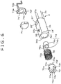
- the slits 38a and 38b and the recessed groove 39 of the cylindrical body 34 can be omitted by forming the construction of the terminal member 72 and the construction of the cylindrical body 34 of the holder portion 3a as shown in FIG. 6 .
- FIG. 6 is a diagram showing the portions of the pressure sensing parts 7 and the holder portion 3a of the board holder 3.
- the terminal member 72 in the example of FIGS. 4A to 4C is changed to a terminal member 72'
- the cylindrical body 34 forming the holder portion 3a in the example of FIGS. 4A to 4C is changed to a cylindrical body 34'.
- the construction of other parts is the same as that shown in FIGS. 4A to 4C .
- the terminal member 72' has a substantially similar construction to that of the terminal member 72 in the example of FIGS. 4A to 4C , but does not have the bulging portions 72a and 72b.
- An L-shaped projection 72f projecting on an opposite side from the lead portion 72d is formed at a position of a lower end portion of the terminal member 72', which lower end portion is on an opposite side from the side of an opening portion 35', the position being such as to be opposed to the L-shaped projection 72e with the swelling portion 72c interposed between the L-shaped projection 72f and the L-shaped projection 72e.
- a distance between the L-shaped projection 72e and the L-shaped projection 72f is in accordance with the size of the dielectric 71.
- the dielectric 71 can be sandwiched and locked between the L-shaped projection 72e and the L-shaped projection 72f.
- the cylindrical body 34' of the holder portion 3a does not have the slits 38a and 38b nor have the recessed groove 39.
- the opening portion 35 is formed by cutting away the cylindrical body 34 by the wall thickness of the cylindrical body 34, and the wall portion 37 and the cylindrical body 34 are lower by the same thickness of the cut-away portion.
- the opening portion 35' corresponding to the opening portion 35 is formed by making a gap in the side circumferential surface of the cylindrical body 34' in a direction orthogonal to the axial direction, and the height of a wall portion 37' corresponding to the wall portion 37 is greater than that of the wall portion 37.
- the lead portion 72d of the terminal member 72 cannot straddle the wall portion 37' as it is.
- a recessed groove 37a, into which to fit the lead portion 72d precisely, is formed in the wall portion 37' in a vertical direction (direction orthogonal to the axial direction).
- the dielectric 71 sandwiched and positioned between the L-shaped projection 72e and the L-shaped projection 72f of the terminal member 72' is inserted and housed into the hollow portion of the cylindrical body 34' in the direction orthogonal to the axial direction through the opening portion 35'.
- the lead portion 72d of the terminal member 72' is fitted into the recessed groove 37a of the wall portion 37', and an end portion of the lead portion 72d is positioned on the side of the printed board 8.
- the dielectric 71 can be positioned by being sandwiched between the L-shaped projection 72e and the L-shaped projection 72f of the terminal member 72' and can be housed into the cylindrical body 34' through the opening portion 35' in the positioned state, which is convenient.
- the cylindrical body 34' is simplified in construction because the slits 38a and 38b and the recessed groove 39 do not need to be formed in the cylindrical body 34'.
- the retaining member when the plurality of parts forming the pen pressure detecting module are inserted into the cylindrical holder from the axial direction, the retaining member needs to press-fit parts into the holder portion. Therefore, contact portions of the engaging portions formed on the parts and the engaging portions of the holder and the casing may be worn away or chipped.
- the position of the parts after the plurality of parts forming the pen pressure detecting module are incorporated into the holder and the casing of the position indicator may differ for each position indicator. Then, positional relation between the parts of the pen pressure detecting module in each position indicator is not constant, so that the characteristics of pen pressure detection may become different.
- FIGS. 7A to 9D are diagrams of assistance in explaining an example of construction of the second embodiment of the position indicator according to the present invention.
- a position indicator 1A according to the second embodiment is an example of a position indicator used in conjunction with the position detecting device 202 provided in the electronic device 200. Only the construction of parts of a plurality of parts forming pressure sensing parts and the construction of a portion corresponding to the holder portion 3a of the board holder 3 in the position indicator 1A according to the second embodiment are different from those of the first embodiment, and the construction of other portions in the position indicator 1A according to the second embodiment is similar to that of the first embodiment. Accordingly, the same portions in the position indicator 1A according to the second embodiment as in the position indicator 1 according to the first embodiment are identified by the same reference symbols, and detailed description thereof will be omitted.
- FIGS. 7A and 7B schematically show the position indicator 1A as a whole according to the second embodiment.
- FIG. 7A shows the inside of a case main body 2a of a case 2 (casing) of the position indicator 1A with only the case main body 2a cut away for purposes of illustration.
- FIG. 7B is a view of the position indicator 1A according to the second embodiment as viewed in an axial direction from the side of a core body 4.
- FIG. 8A is a sectional view taken along line X'-X' of FIG. 7B , and is a partial sectional view of the position indicator 1A sectioned in a direction passing through the axial position of the position indicator 1A and parallel with a board surface (surface on which a conductor pattern is printed and formed and circuit parts are mounted) 8a of a printed board 8.
- FIG. 8B is a sectional view taken along line Y'-Y' of FIG. 7B , and is a partial sectional view of the position indicator 1A sectioned in a direction passing through the axial position of the position indicator 1A and perpendicular to the board surface 8a of the printed board 8.
- FIG. 8C is a perspective view directing attention to a holder portion 3Aa, in particular, of a board holder 3A according to the second embodiment.
- the board holder 3A in the second embodiment has the holder portion 3Aa and a printed board mounting base portion 3Ab.
- FIG. 9B is a diagram showing a state in which the core body 4 and a ferrite core 6 are coupled to the board holder 3A.
- FIG. 9A is an exploded perspective view of assistance in explaining the holder portion 3Aa of the board holder 3A and pressure sensing parts 7A.
- the printed board mounting base portion 3Ab is formed in a similar manner to the printed board mounting base portion 3b of the board holder 3 in the first embodiment, as shown in FIG. 9B .
- the board holder 3A has a flat surface 3Apn formed along the axial direction on a side of a side circumferential surface of a cylindrical body 34A forming the holder portion 3Aa, which side is opposed to an opening portion 35A to be described later with the axial position interposed therebetween and is opposite from the printed board mounting flat surface of the printed board mounting base portion 3Ab.
- the flat surface 3Apn is a flush flat surface along the axial direction on the holder portion 3Aa or from the holder portion 3Aa to the printed board mounting base portion 3Ab.
- the pen pressure detecting module in the present example uses a variable capacitance capacitor whose capacitance varies according to pen pressure applied to the core body as in the first embodiment.
- the pressure sensing parts 7A in the present example are formed by a plurality of parts, that is, a dielectric 71, a terminal member 72, a retaining member 73A, a conductive member 74, and an elastic member 75. That is, the pressure sensing parts 7A have a similar construction to that of the first embodiment except that the retaining member 73A has a different construction from that of the retaining member 73 in the first embodiment.
- the holder portion 3Aa of the board holder 3A is formed by the cylindrical body 34A having a hollow portion, and is formed so as to house the pressure sensing parts 7A arranged in the axial direction within the hollow portion of the cylindrical body 34A.
- all of the pressure sensing parts 7A are inserted in a direction orthogonal to the axial direction of the cylindrical body 34A and perpendicular to the board surface 8a of the printed board 8, through the opening portion 35A formed in a portion of the side circumferential surface of the cylindrical body 34A forming the holder portion 3Aa and opened in the direction orthogonal to the axial direction, as shown in FIG. 9A , and are housed as shown in FIGS. 8A to 8C .
- FIG. 9C is a sectional view taken along line B-B in the cylindrical body 34A forming the holder portion 3Aa of FIG. 9A , and is a sectional view obtained by cutting away a portion of the opening portion 35A in about the middle in the axial direction of the cylindrical body 34A in the direction orthogonal to the axial direction.
- FIG. 9D is a sectional view taken along line C-C in the cylindrical body 34A forming the holder portion 3Aa of FIG. 9A , and is a sectional view obtained by cutting away the cylindrical body 34A in the axial direction thereof.
- the opening portion 35A formed in a portion of the side circumferential surface of the cylindrical body 34A is opened in the direction orthogonal to the axial direction and opened in the direction perpendicular to the board surface 8a of the printed board 8 mounted on the printed board mounting base portion 3Ab.
- the opening portion 35A has a predetermined length d5 (see FIG. 9D ) in the axial direction, and has a predetermined length d6 (see FIG. 9C ) in a direction orthogonal to the axial direction.
- the length d5 is selected to be slightly larger than the entire length of the pressure sensing parts 7A as a whole arranged in the axial direction, which length is obtained when the pressure sensing parts 7A are compressed in the axial direction against the biasing force of the elastic member 75.
- the length d6 is selected to be slightly larger than the largest length of the lengths of the plurality of parts forming the pressure sensing parts 7A in the direction orthogonal to the axial direction.
- the cylindrical body 34A forming the holder portion 3Aa has an opening 36Aa of an inside diameter d7 (see FIG. 9D ) on the side of the core body 4 in the axial direction of the cylindrical body 34A, and has the construction of a ring-shaped locking portion 36A having no openings on the side circumferential surface.
- the inside diameter d7 of the ring-shaped locking portion 36A is selected to be smaller than the inside diameter d6 of the portion in about the middle of the cylindrical body 34A, in which portion the opening portion 35A is formed (d7 ⁇ d6).
- the hollow portion of the cylindrical body 34A has a stepped portion 34Ac formed between the ring-shaped locking portion 36A and the portion of the inside diameter d6 of the cylindrical body 34A, in which portion the opening portion 35A is formed.
- the cylindrical body 34A forming the holder portion 3Aa is closed by a wall portion 37A on the side of the printed board mounting base portion 3Ab.
- a locking portion 32 is formed on the wall portion 37A on the side of the printed board mounting base portion 3Ab.
- Slits 38Aa and 38Ab having a predetermined width in the axial direction are formed in a coupling portion of the side circumferential surface of the cylindrical body 34A, which coupling portion is coupled to the wall portion 37A.
- the dielectric 71 of the pressure sensing parts 7A is formed as a plate-shaped object having an external shape to be fitted into the recessed groove 39A and having a thickness corresponding to the width in the axial direction of the recessed groove 39A. Therefore, the dielectric 71 can be inserted and fitted into the recessed groove 39A of the cylindrical body 34A through the opening portion 35A, and the recessed groove 39A prevents the dielectric 71 in the fitted state from moving in the axial direction within the cylindrical body 34A.
- the terminal member 72 in the second embodiment is formed by a disk-shaped conductive member, for example a plate-shaped object of a conductive metal, which has the same thickness as the width in the axial direction of the slits 38Aa and 38Ab of the cylindrical body 34A and has an outside diameter corresponding to the inside diameter d6. As shown in FIG. 9A , the terminal member 72 has bulging portions 72Aa and 72Ab to be fitted into the slits 38Aa and 38Ab of the cylindrical body 34A.
- the terminal member 72 can be inserted so as to be in contact with the wall portion 37A of the cylindrical body 34A through the opening portion 35A, and the bulging portions 72Aa and 72Ab are fitted into the slits 38Aa and 38Ab of the cylindrical body 34A by the insertion and locked to the cylindrical body 34A.
- a swelling portion 72c swelling on the side of the dielectric 71 is formed on a central portion of a plate surface of the terminal member 72, which plate surface is on the side of the dielectric 71.
- the swelling portion 72c plays a role of surely bringing the dielectric 71 and the terminal member 72 into contact with each other when the dielectric 71 and the terminal member 72 are housed within the cylindrical body 34A.
- the terminal member 72 has a lead portion 72d straddling the wall portion 37A of the cylindrical body 34A to be connected by soldering to a land portion 8b (see FIG. 8C ) on the board surface 8a of the printed board 8 mounted on the printed board mounting base portion 3Ab.
- the retaining member 73A has a cylindrical shape including a ring-shaped swelling portion 73Ai in a portion in a circumferential direction of a side circumferential surface of the retaining member 73A.
- the retaining member 73A has a cylindrical shape portion 73Aa having a recessed hole 73Ab, into which to press-fit the core body main body 42 of the core body 4 on the core body 4 side in the axial direction of the retaining member 73A.
- the retaining member 73A also has a ring-shaped projecting portion 73Ac having a recessed hole 73Ad, into which to fit the conductive member 74 on an opposite side in the axial direction from the side of the recessed hole 73Ab.
- the center line positions of the ring-shaped swelling portion 73Ai, the cylindrical shape portion 73Aa, and the ring-shaped projecting portion 73Ac are the same as the center line position of the retaining member 73A of a cylindrical shape, and the recessed hole 73Ab and the recessed hole 73Ad are formed such that the center line (axial position) of the recessed hole 73Ab and the center line (axial position) of the recessed hole 73Ad are located on one straight line.
- the outside diameter (portion in a circumferential direction) of the ring-shaped swelling portion 73Ai of the retaining member 73A is selected to be equal to the inside diameter d6 of the inside portion of the opening portion 35A of the cylindrical body 34A.
- the outside diameter of the cylindrical shape portion 73Aa of the retaining member 73A is selected to be slightly smaller than the inside diameter of the ring-shaped locking portion 36A of the cylindrical body 34A.
- the diameter of the recessed hole 73Ab of the cylindrical shape portion 73Aa is selected to be slightly smaller than the diameter of the core body main body 42 of the core body 4.
- the length (height) in the axial direction of the cylindrical shape portion 73Aa is shorter than the length in the axial direction of the ring-shaped locking portion 36A of the cylindrical body 34A, and is about 1/2 of the length in the axial direction of the ring-shaped locking portion 36A of the cylindrical body 34A in the present example.
- the outside diameter of the ring-shaped projecting portion 73Ac of the retaining member 73A is selected to be smaller than the diameter d6 of the inside of the opening portion 35A of the cylindrical body 34A and smaller than the inside diameter of a coil spring forming the elastic member 75.
- the inside diameter of the ring-shaped projecting portion 73Ac is selected to be substantially equal to the outside diameter of a small-diameter portion 74b of the conductive member 74.
- slits 73Ae and 73Af are formed in the cylindrical shape portion 73Aa and the ring-shaped projecting portion 73Ac so as to traverse the recessed hole 73Ab and the recessed hole 73Ad, respectively.
- the presence of the slits 73Ae and 73Af allows the cylindrical shape portion 73Aa and the ring-shaped projecting portion 73Ac to be elastically displaced in the direction orthogonal to the axial direction.
- the core body main body 42 and the conductive member 74 are easily press-fitted into the recessed hole 73Ab and the recessed hole 73Ad of the cylindrical shape portion 73Aa and the ring-shaped projecting portion 73Ac, respectively.
- the retaining member 73A has the construction as described above.
- the cylindrical shape portion 73Aa is housed within the ring-shaped locking portion 36A of the cylindrical body 34A, and an (axial) end surface of the ring-shaped swelling portion 73Ai abuts against an (axial) end surface of the ring-shaped locking portion 36A of the cylindrical body 34A, whereby the retaining member 73A is prevented from moving to the side of the core body 4. That is, the stepped portion 34Ac of the cylindrical body 34A prevents the retaining member 73A from moving in the axial direction to the side of the core body 4.
- the conductive member 74 is similar to that of the first embodiment.
- the outside diameter of a large-diameter portion 74a is selected to be equal to the outside diameter of the ring-shaped projecting portion 73Ac of the retaining member 73A
- the outside diameter of the small-diameter portion 74b is selected to be substantially equal to the diameter of the recessed hole 73Ad of the ring-shaped projecting portion 73Ac of the retaining member 73A.
- a winding portion 75a of the coil spring having conductivity, which coil spring forms the elastic member 75, has such a diameter as to be able to house the conductive member 74 and the ring-shaped projecting portion 73Ac of the retaining member 73A within the winding portion 75a without being in contact with the conductive member 74 and the ring-shaped projecting portion 73Ac of the retaining member 73A and as to be smaller than the outside diameter of the cylindrical shape portion 73Aa of the retaining member 73A.
- a connecting portion 75c of the elastic member 75 is inserted from the notch portion of the ring-shaped projecting portion 73Ac of the retaining member 73A into the inside of the ring-shaped projecting portion 73Ac (see FIG. 8A and FIG. 8B ).
- a terminal piece 75b of the elastic member 75 straddles the dielectric 71, the terminal member 72, and the wall portion 37A, and is connected by soldering to the conductive pattern on the board surface 8a of the printed board 8 mounted on the printed board mounting base portion 3Ab.
- the board holder 3A is mounted on the flat surface of the workbench such that the flat surface 3Apn faces the flat surface of the workbench.
- the board holder 3A is positioned such that the opening of the opening portion 35A faces in an upward direction orthogonal to the flat surface of the workbench and the printed board mounting flat surface of the printed board mounting base portion 3Ab is parallel to the flat surface of the workbench, and the board holder 3A is locked on the flat surface of the workbench.
- the small-diameter portion 74b of the conductive member 74 is first press-fitted into the ring-shaped projecting portion 73Ac of the retaining member 73A, and the winding portion 75a of the elastic member 75 is arranged so as to be brought around the periphery of the ring-shaped projecting portion 73Ac and the conductive member 74.
- the connecting portion 75c of the elastic member 75 is sandwiched between the upper end surface of the small-diameter portion 74b of the conductive member 74 and the bottom of the retaining member 73A, which bottom is surrounded by the ring-shaped projecting portion 73Ac, so that the connecting portion 75c of the elastic member 75 and the conductive member 74 are electrically connected to each other.
- the dielectric 71 is disposed so as to be opposed to a curved surface of the conductive member 74, which curved surface is in the form of a shell, and further the terminal member 72 is disposed so as to be superposed on the dielectric 71.
- the retaining member 73A, the conductive member 74 and the elastic member 75, the dielectric 71, and the terminal member 72 are arranged in this order in the axial direction.
- the pressure sensing parts 7A as a whole are sandwiched between the end surface of the cylindrical shape portion 73Aa of the retaining member 73A and an end surface of the terminal member 72, which end surface is on the opposite side from the dielectric 71.
- the pressure sensing parts 7A as a whole are sandwiched with the elastic member 75 biased so as to be compressed in the axial direction.
- a dedicated jig can be used for this sandwiching.
- the length in the axial direction of the pressure sensing parts 7A as a whole, when the pressure sensing parts 7A are thus sandwiched by the jig is slightly shorter than the length d5 in the axial direction of the opening portion 35A of the cylindrical body 34A forming the holder portion 3Aa.
- the pressure sensing parts 7A as a whole that are being sandwiched by the jig are housed into the cylindrical body 34A in the direction orthogonal to the axial direction through the opening portion 35A of the cylindrical body 34A so as to fit the bulging portions 72Aa and 72Ab of the terminal member 72 into the slits 38Aa and 38Ab of the cylindrical body 34A and so as to fit the dielectric 71 into the recessed groove 39A. Only the jig is removed. Then, the elastic member 75 produces a bias by expanding in the axial direction.
- the bias in the axial direction by the elastic member 75 is applied to only the retaining member 73A, in which the conductive member 74 is press-fitted.
- the cylindrical shape portion 73Aa of the retaining member 73A is inserted and fitted into the ring-shaped locking portion 36A of the cylindrical body 34A, and the ring-shaped swelling portion 73Ai of the retaining member 73A is engaged with the stepped portion 34Ac of the cylindrical body 34A, thus preventing the retaining member 73A from moving toward the core body 4 in the axial direction within the cylindrical body 34A.
- the retaining member 73A is also prevented from moving in the direction orthogonal to the axial direction. Further, in this state, the elastic member 75 applies the biasing force in the axial direction to the plurality of parts as a whole forming the pressure sensing parts 7A. Therefore, the pressure sensing parts 7A as a whole are prevented from being displaced in the axial direction or falling out through the opening portion 35A.
- a locking mechanism which is configured to prevent the plurality of parts as a whole forming the pressure sensing parts 7A from being displaced in the direction orthogonal to the axial direction, is provided by the engagement between the ring-shaped locking portion 36A of the cylindrical body 34A and the cylindrical shape portion 73Aa of the retaining member 73A and the biasing force of the elastic member 75.
- the lead portion 72d of the terminal member 72 is soldered to the land portion 8b of the printed board 8, and the terminal piece 75b of the elastic member 75 is soldered to the printed board 8.
- the soldering and fixing of the lead portion 72d of the terminal member 72 and the terminal piece 75b of the elastic member 75 to the printed board 8 can more surely prevent the pressure sensing parts 7A from falling out through the opening portion 35A.
- the dielectric 71 and the terminal member 72 are housed in a state of being unable to move in the axial direction within the hollow portion of the cylindrical body 34A.
- the retaining member 73A fitted with the conductive member 74 is movable in the axial direction within the hollow portion of the cylindrical body 34A.
- the biasing force of the elastic member 75 biases the retaining member 73A to the side of the ring-shaped locking portion 36A of the cylindrical body 34A, with an air space created between the conductive member 74 and the dielectric 71.
- an anti-falling member 9 is press-fitted into the ring-shaped locking portion 36A of the cylindrical body 34A, as shown in FIGS. 8A and 8B and FIG. 9B .
- the anti-falling member 9 is coupled to the holder portion 3Aa by press-fitting a cylindrical portion 9b of the anti-falling member 9 into the ring-shaped locking portion 36A of the cylindrical body 34A.
- the ferrite core 6 is coupled to the holder portion 3Aa of the board holder 3A via the anti-falling member 9.
- the core body main body 42 of the core body 4 is inserted into a through hole 6a of the ferrite core 6, and an end portion of the core body main body 42 of the core body 4 is press-fitted into the recessed hole 73Ab of the cylindrical shape portion 73Aa of the retaining member 73A housed in the holder portion 3Aa.
- the core body main body 42 of the core body 4 is also exposed from the ferrite core 6 to the side of the projecting member 41 of the core body 4, as shown in FIG. 8A and FIG. 9B .
- a pressure (pen pressure) applied to the projecting member 41 of the core body 4 can displace the core body 4 toward the side of a case cap 2b in the axial direction against the biasing force of the elastic member 75.
- the printed board 8 is mounted on the printed board mounting base portion 3Ab of the board holder 3A coupled to the case cap 2b, the pressure sensing parts 7A are housed in the holder portion 3Aa, and the ferrite core 6 and the core body 4 are coupled to the holder portion 3Aa, whereby a module part as shown in FIG. 9B is formed.
- the module part is inserted into the hollow portion of the case main body 2a, so that the projecting member 41 of the core body 4 projects from a through hole 21 of the case main body 2a to the outside. Then, the case main body 2a and the case cap 2b are coupled to each other, whereby the position indicator 1A is completed.
- Pen pressure detecting operation in the position indicator 1A is the same as that of the foregoing first embodiment, and therefore description thereof will be omitted here.
- the pen pressure detecting module can be created by housing all of the plurality of parts forming the pressure sensing parts 7A into the holder portion 3Aa in the direction orthogonal to the axial direction through the opening portion 35A having an opening in the direction orthogonal to the axial direction, the opening portion 35A being provided in the side circumferential surface of the cylindrical body 34A forming the holder portion 3Aa.
- all of the plurality of parts forming the pressure sensing parts 7A are arranged in the axial direction into a unit, and the unit of the parts can be housed into the holder portion 3Aa in the direction orthogonal to the axial direction through the opening portion 35A in a state of being sandwiched from both sides in the axial direction of the unit of the parts.
- the parts can be retained in a state in which the center line position of the case 2 and the center line position of the pressure sensing parts 7A coincide with each other, by housing the parts within the holder portion 3Aa such that the parts are merely arranged along the axial direction.
- the retaining member 73A among the pressure sensing parts 7A in the state of being housed in the hollow portion of the cylindrical body 34A is moved by the elastic member 75 to the side of the core body 4 in the axial direction, to be engaged with the ring-shaped locking portion 36A and locked so as not to move in the direction orthogonal to the axial direction.
- the pen pressure detecting module can be manufactured more easily, and work efficiency in the manufacturing of the position indicator is improved, so that the position indicator is suitable for mass production.
- the second embodiment also provides similar effects to those of the foregoing first embodiment.
- the second embodiment in particular provides the following effects as compared with the case where the conventional variable capacitance capacitor described with reference to FIGS. 19A and 19B is used as pressure sensing parts.
- the retaining member 105 is press-fitted into the hollow portion of the holder 102. At this time, portions of the engaging holes 102d and 102e of the holder 102, which engaging holes are brought into contact with the engaging projecting portions 105d and 105e provided to the retaining member 105, may be worn away or chipped, so that the position in the axial direction of the retaining member 105 with respect to the holder 102 after assembly may be varied. When such a variation occurs, a distance before contact between the conductive member 106 and the dielectric 103 may be varied, and thus the characteristics of the variable capacitance capacitor may be varied in each position indicator.
- the retaining member 73A is engaged with the ring-shaped locking portion 36A by the biasing force of the elastic member 75 by merely inserting the retaining member 73A into the cylindrical body 34A forming the holder portion 3Aa in the direction orthogonal to the axial direction through the opening portion 35A. Therefore, unlike the position in the axial direction of the retaining member 105 that varies relative to the holder 102 in the prior art example of FIGS. 19A and 19B , the position of the retaining member 73A with respect to the holder portion 3Aa does not vary, and the characteristics of the variable capacitance capacitor are not varied in each position indicator.
- the terminal member 104 needs to elastically hold down the dielectric 103 and fix the dielectric 103 to the holder 102.
- the terminal member 104 thus needs to have a shape larger than the diameter of the dielectric 103. Therefore, the conventional variable capacitance capacitor has a large size, and is difficult to be made thinner.
- the pressure sensing parts 7A are merely housed into the holder portion 3Aa in the direction orthogonal to the axial direction through the opening portion 35A and arranged in the axial direction, and the terminal member 72 can be of substantially the same shape as the dielectric 71. Therefore the position indicator can be thinned easily by miniaturizing each of the plurality of parts forming the pressure sensing parts 7A so as to correspond to the thinning of the position indicator.
- the dielectric 71 can be more surely prevented from falling out through the opening portion 35A of the holder portion 3Aa by providing the terminal member 72 with an L-shaped projection for holding down an end portion of the dielectric 71 housed in the holder portion 3Aa, the end portion of the dielectric 71 being on the side of the opening portion 35A, in the direction orthogonal to the axial direction.
- a third embodiment of the position indicator according to the present invention will next be described with reference to FIGS. 10 to 14 .
- the position indicators 1 and 1A according to the first embodiment and the second embodiment use a variable capacitance capacitor for pen pressure detection.
- a position indicator 1B according to the third embodiment detects a change in inductance value of a coil forming a resonance circuit for pen pressure detection.
- the position indicator 1B according to the third embodiment is used in conjunction with a position detecting device 202B included in the electronic device 200 shown in FIG. 2 .
- the position detecting device 202B uses a pen pressure detecting method different from that of the position detecting device 202.
- a circuit of the position indicator 1B and a circuit configuration of the position detecting device 202B will be described later.
- the same parts as in the first embodiment and the second embodiment are identified by the same reference numerals, and detailed description thereof will be omitted.
- parts corresponding to the respective parts in the first embodiment and the second embodiment are identified by the same reference numerals to which a suffix B is added.
- FIG. 10 schematically shows the position indicator 1B as a whole according to the third embodiment.
- FIG. 10 shows the inside of a case main body 2Ba of a case 2B of the position indicator 1B with only the case main body 2Ba cut away for purposes of illustration.
- an end portion in a longitudinal direction of the board holder 3B is coupled to a case cap 2Bb at a coupling portion 3Bc of the board holder 3B.
- the core body 4B includes a projecting member (pen point member) 41B and a ferrite core 6B.
- the pressure sensing parts 7B include a ferrite chip 701, a coil spring 702, and an elastic body, or a silicon rubber 703 in the present example.
- the ferrite core 6B is an example of a first magnetic substance
- the ferrite chip 701 is an example of a second magnetic substance.
- the projecting member 41B of the core body 4B is housed with a portion of the projecting member 41B projected through a through hole 21B.
- the projecting member 41B has a flange portion 41Ba.
- the flange portion 41Ba is engaged with a stepped portion 22B formed in the portion of the through hole 21B of the case main body 2Ba, so that the projecting member 41B is prevented from falling out through the through hole 21B.
- the projecting member 41B is made of a synthetic resin such as a polyacetal resin (Duracon) or the like in consideration of resistance to friction when the projecting member 41B is used in a state of abutting against an operating surface.
- the ferrite core 6B in the present example has a cylindrical shape without a through hole.
- the ferrite core 6B forming a portion of the core body 4B has a flange portion 6Ba having a diameter larger than a winding portion of the coil 5B on an opposite side from the side of the projecting member 41B.
- the flange portion 6Ba is locked by a pressure sensing part holder portion 3Ba (which will be abbreviated to a holder portion 3Ba) to be described later of the board holder 3B.
- the ferrite core 6B is thereby locked to and retained by the board holder 3B.
- the board holder 3B has the holder portion 3Ba on the side of the core body 4B and a printed board mounting base portion 3Bb formed so as to be continuous with the holder portion 3Ba on an opposite side from the side of the core body 4B.
- the ferrite chip 701, the coil spring 702, and the silicon rubber 703 forming the pressure sensing parts 7B are arranged in order and retained in an axial direction along a direction of going from the side of the printed board mounting base portion 3Bb to the side of the core body 4B. Further, a printed board 8B is mounted on the printed board mounting base portion 3Bb of the board holder 3B.
- a side switch 11, capacitors 12 and 13, and other parts and a conductive pattern are provided on a board surface 8Ba of the printed board 8B as in the first embodiment and the second embodiment.
- an IC 14 and a peripheral circuit thereof are not provided on the printed board 8B.
- the printed board 8B in a state of being mounted and locked on the printed board mounting base portion 3Bb is separated from an inner wall of the case main body 2Ba without being in contact with the inner wall of the case main body 2Ba.
- FIGS. 11A to 11C are diagrams of assistance in explaining the construction of portions housed within the case main body 2Ba of the position indicator 1B.
- FIG. 11B is a perspective view of the board holder 3B.
- FIG. 11A is a diagram of the parts retained by the board holder 3B, the parts being shown arranged in the axial direction of the case main body 2Ba.
- FIG. 11C is a diagram showing a state in which the ferrite core 6B and the pressure sensing parts 7B are housed and retained in the board holder 3B and the printed board 8B is disposed and locked on the board holder 3B.
- the parts retained by the holder portion 3Ba of the board holder 3B are the flange portion 6Ba of the ferrite core 6B (wound with the coil 5B) of the core body 4B and all of the plurality of parts forming the pressure sensing parts 7B.
- the printed board 8B is mounted on the printed board mounting base portion 3Bb of the board holder 3B.
- a rod-shaped member 704 disposed next to the ferrite chip 701 in the axial direction is a locking member for locking the ferrite chip 701 of the pressure sensing parts 7B to the holder portion 3Ba in a state in which the center line position of the ferrite chip 701 and the center line position of the holder portion 3Ba coincide with each other.
- the holder portion 3Ba has a shape provided with an opening portion 35B formed by cutting away, along the axial direction, an overall length of a side circumferential surface of a cylindrical body 34B in a cylindrical shape corresponding to the hollow portion of the case main body 2Ba.
- the opening portion 35B has an opening in a direction orthogonal to the axial direction of the cylindrical body 34B and orthogonal to the mounting flat surface of the printed board mounting base portion 3Bb of the board holder 3B, on which mounting flat surface the printed board 8B is mounted.
- a core body locking portion 36B is formed in an end portion of the cylindrical body 34B forming the holder portion 3Ba, which end portion is on the side of the core body 4B.
- a part arranging portion 320 for arranging the pressure sensing parts 7B is formed in the holder portion 3Ba so as to be continuous with the core body locking portion 36B.
- the opening portion 35B is formed over the core body locking portion 36B and the part arranging portion 320.
- an opening 36Ba is made on the core body 4B side of the cylindrical body 34B forming the holder portion 3Ba, and a wall portion 37B that closes the hollow portion of the cylindrical body 34B is formed at an end portion of the cylindrical body 34B, which end portion is on the side of the printed board mounting base portion 3Bb.
- the flange portion 6Ba of the ferrite core 6B as well as the silicon rubber 703, the coil spring 702, and the ferrite chip 701 forming the pressure sensing parts 7B are arranged in the axial direction, and housed in the core body locking portion 36B and the part arranging portion 320 of the holder portion 3Ba through the opening portion 35B.
- the printed board mounting base portion 3Bb is formed between the coupling portion 3Bc of the board holder 3B, which coupling portion is an end portion of the board holder 3B on the side of the case cap 2Bb in the axial direction, and the wall portion 37B of the holder portion 3Ba.
- the printed board 8B that is long and thin with a width smaller than the inside diameter of the case main body 2Ba is mounted on the printed board mounting base portion 3Bb.
- a locking portion 33B for locking the printed board 8B to the printed board mounting base portion 3Bb by sandwiching an end portion in a longitudinal direction of the printed board 8B in a direction of thickness thereof is formed on the case cap 2Bb side of the printed board mounting base portion 3Bb.
- no locking portion is formed on the wall portion 37B of the cylindrical body 34B forming the holder portion 3Ba, which wall portion is on the side of the printed board mounting base portion 3Bb.
- a portion of the above-described rod-shaped member 704 is located on the side of the printed board mounting base portion 3Bb, and thereby serves also as a locking portion for sandwiching a thickness portion of an end portion of the printed board 8B between the locking portion and the mounting flat surface of the printed board mounting base portion 3Bb.
- FIGS. 12A to 12D are diagrams showing an example of construction of the board holder 3B.
- FIG. 12A is a top view of the board holder 3B as viewed in a direction orthogonal to the mounting flat surface of the printed board mounting base portion 3Bb.
- FIG. 12B is a side view of the board holder 3B as viewed in a direction parallel to the mounting flat surface of the printed board mounting base portion 3Bb.
- FIG. 12C is a sectional view taken along line D-D of FIG. 12A.
- FIG. 12D is a sectional view taken along line E-E of FIG. 12C .
- FIG. 13 is a diagram of assistance in explaining a housed and retained state of the ferrite core 6B and the pressure sensing parts 7B in the core body locking portion 36B and the part arranging portion 320 of the holder portion 3Ba of the board holder 3B.
- FIG. 13 shows the holder portion 3Ba in a state of the sectional view of FIG. 12C for purposes of illustration.
- a flat surface 3Bpn is formed along the axial direction on a side of a side circumferential surface of the cylindrical body 34B forming the holder portion 3Ba, which side is opposed to the opening portion 35B with the axial core interposed therebetween and is opposite from the printed board mounting flat surface of the printed board mounting base portion 3Bb.
- the flat surface 3Bpn is a flush flat surface along the axial direction on the holder portion 3Ba or from the holder portion 3Ba to the printed board mounting base portion 3Bb.
- the inside diameter of the core body locking portion 36B is selected to be slightly larger than the diameter of the portion of the ferrite core 6B wound with the coil 5B.
- the part arranging portion 320 is formed continuously with the core body locking portion 36B.
- a coupling portion of the part arranging portion 320, which coupling portion is coupled to the core body locking portion 36B, is formed so as to have an inside diameter slightly larger than the outside diameter of the flange portion 6Ba of the ferrite core 6B.
- a stepped portion 34Bc is formed at the coupling portion of the part arranging portion 320, which coupling portion is coupled to the core body locking portion 36B.
- the flange portion 6Ba of the ferrite core 6B is disposed on the part arranging portion 320 side of the core body locking portion 36B.
- the stepped portion 34Bc thereby locks the ferrite core 6B so as to prevent the core body 4B from falling off the holder portion 3Ba in the axial direction.
- the part arranging portion 320 includes a notch for receiving the flange portion 6Ba of the ferrite core 6B.
- the ferrite core 6B is formed such that an angular-range of at least 180 degrees of the flange portion 6Ba of the ferrite core 6B is retained in the core body locking portion 36B.
- the ferrite core 6B is retained so as not to be detached from the core body locking portion 36B and not to fall out in the direction orthogonal to the axial direction in a state in which the center line position of the ferrite core 6B coincides with the center line position of the cylindrical body 34B forming the holder portion 3Ba.
- the silicon rubber 703 of the pressure sensing parts 7B has a projecting portion 703a.
- an end surface of the flange portion 6Ba of the ferrite core 6B has a recessed hole 6Bb, into which to fit the projecting portion 703a of the silicon rubber 703.
- the silicon rubber 703 is mounted on the end surface of the flange portion 6Ba of the ferrite core 6B by press-fitting the projecting portion 703a of the silicon rubber 703 into the recessed hole 6Bb of the flange portion 6Ba of the ferrite core 6B.
- the outside diameter of the silicon rubber 703 is selected to be smaller than the diameter of the end surface of the flange portion 6Ba of the ferrite core 6B.
- the pressure sensing parts 7B are retained in the part arranging portion 320 such that the coil spring 702 forms a predetermined air space Ar between an end surface of the ferrite chip 701 and the silicon rubber 703 mounted on the end surface of the flange portion 6Ba of the ferrite core 6B.
- the part arranging portion 320 has the wall portion 37B that an end surface of a flange portion 701a of the ferrite chip 701 abuts against, thus preventing the ferrite chip 701 from moving to the side of the printed board mounting base portion 3Bb in the axial direction.
- a through hole 320e, into which to insert the rod-shaped member 704, is formed in a position of the wall portion 37B, which position corresponds to the center position of the cylindrical body 34B forming the holder portion 3Ba.
- a fitting recessed portion 320a having an inside diameter equal to or slightly larger than the outside diameter of the flange portion 701a of the ferrite chip 701 is formed in the part arranging portion 320 by a distance corresponding to the thickness of the flange portion 701a in a direction of going from the wall portion 37B to the side of the core body locking portion 36B.
- a step portion 320b having an inside diameter equal to or slightly larger than the outside diameter of a small-diameter portion of the ferrite chip 701 excluding the flange portion 701a is formed on the core body locking portion 36B side of the fitting recessed portion 320a.
- a portion located farther inside on the core body locking portion 36B side of the step portion 320b is a coil disposing portion 320c having an inside diameter equal to that of the portion whose inside diameter is made slightly larger than the flange portion 6Ba of the ferrite core 6B to form the stepped portion 34Bc.
- the length in the axial direction of the coil disposing portion 320c is a length from the position of the stepped portion 34Bc formed with the core body locking portion 36B to the position of a stepped portion 320d formed between the coil disposing portion 320c and the step portion 320b.
- the length in the axial direction of the coil disposing portion 320c is such that the pressure sensing parts 7B can be retained in a state in which the predetermined air space Ar is formed between the end surface of the ferrite chip 701, which end surface is on the opposite side in the axial direction from the flange portion 701a, and the silicon rubber 703 mounted on the end surface of the flange portion 6Ba of the ferrite core 6B, as described above.
- the ferrite core 6B having the silicon rubber 703 mounted on the end surface of the flange portion 6Ba is disposed on the core body locking portion 36B side of the coil disposing portion 320c.
- the flange portion 701a of the ferrite chip 701 is fitted in the fitting recessed portion 320a of the part arranging portion 320 in a state of abutting against the wall portion 37B.
- the flange portion 701a is made unable to move in the axial direction by a stepped portion formed by the fitting recessed portion 320a and the step portion 320b.
- the coil spring 702 has a larger winding diameter than the outside diameter of the silicon rubber 703. Therefore, as shown in FIG. 10 and FIG. 13 , one end side of the coil spring 702 in an elastic biasing direction abuts against the end surface of the flange portion 6Ba of the ferrite core 6B in a state of housing the silicon rubber 703 within the winding diameter of the coil spring 702. Another end side of the coil spring 702 in the elastic biasing direction abuts against the stepped portion 320d formed between the step portion 320b and the coil disposing portion 320c.
- the coil spring 702 sets the ferrite core 6B in a state of being elastically biased to the pen point side at all times and locked and retained by the core body locking portion 36B.
- the silicon rubber 703 is fitted and mounted on the ferrite core 6B, the coil spring 702 is then mounted on the small-diameter portion of the ferrite chip 701, and further the silicon rubber 703 is inserted into the winding diameter of the coil spring 702, so that a unit is formed in a state in which the silicon rubber 703 mounted on the ferrite core 6B and the end surface of the ferrite chip 701 are provisionally coupled to each other.
- the unit of the parts is sandwiched by a jig in the axial direction.
- the unit of the parts is sandwiched by the jig between a step portion between the flange portion 6Ba of the ferrite core 6B and the main body of the ferrite core 6B and a head portion of the flange portion 701a of the ferrite chip 701.
- the jig in the state of thus sandwiching the plurality of parts is inserted into the part arranging portion 320 of the holder portion 3Ba in the direction orthogonal to the axial direction through the opening portion 35B.
- the jig is removed, so that the above-described unit of the parts is left in the part arranging portion 320.
- the flange portion 701a of the ferrite chip 701 is fitted into the fitting recessed portion 320a, and the coil spring 702 is inserted so as to abut against the end surface of the flange portion 6Ba of the ferrite core 6B and the stepped portion 320d formed between the step portion 320b and the coil disposing portion 320c.
- the coil spring 702 sets the ferrite core 6B in a state of being elastically biased to the side of the core body locking portion 36B at all times and retained with the air space Ar created between the silicon rubber 703 and the end portion of the small-diameter portion of the ferrite chip 701, as shown in FIG. 10 and FIG. 13 .
- a recessed hole 701b is formed in the center position of the end surface of the flange portion 701a of the ferrite chip 701.
- the rod-shaped member 704 is fitted into the recessed hole 701b through the through hole 320e of the wall portion 37B.
- the ferrite chip 701 is thereby retained such that the center line position of the ferrite chip 701 coincides with the center line position of the cylindrical body 34B forming the holder portion 3Ba.
- the flange portion 6Ba of the ferrite core 6B is displaced to the side of the core body locking portion 36B by the biasing force of the coil spring 702, so that a portion of the flange portion 6Ba is engaged with the inner wall surface of the core body locking portion 36B.
- the ferrite core 6B is thereby locked so as not to move in the direction orthogonal to the axial direction.
- the ferrite chip 701 is also locked so as not to move in the axial direction by the elastic biasing force of the coil spring 702.
- the ferrite core 6B is retained by the core body locking portion 36B such that the center line position of the ferrite core 6B coincides with the center line position of the cylindrical body 34B forming the holder portion 3Ba.
- the parts arranged in the part arranging portion 320 are retained such that the center line positions of the respective parts arranged in the part arranging portion 320 all coincide with the center line position of the cylindrical body 34B forming the holder portion 3Ba.
- the printed board 8B is mounted on the mounting flat surface of the printed board mounting base portion 3Bb of the board holder 3B. At the same time, an end edge of the printed board 8B on the side of the case cap 2Bb in the longitudinal direction of the printed board 8B is locked in a state of being sandwiched between the locking portion 33B and the mounting flat surface of the printed board mounting base portion 3Bb, and an end edge of the printed board 8B on the side of the part arranging portion 320 in the longitudinal direction of the printed board 8B is locked in a state of being sandwiched between the rod-shaped member 704 and the mounting flat surface of the printed board mounting base portion 3Bb.
- the projecting member 41B is mounted on an end of the ferrite core 6B in a state in which the ferrite core 6B wound with the coil 5B and the pressure sensing parts 7B are retained by the holder portion 3Ba of the board holder 3B, and the printed board 8B is mounted and locked on the printed board mounting base portion 3Bb as described above.
- an object formed by mounting and locking the printed board 8B on the printed board mounting base portion 3Bb of the board holder 3B, housing the pressure sensing parts 7B in the holder portion 3Ba and housing a portion of the ferrite core 6B wound with the coil 5B in the holder portion 3Ba, and coupling the projecting member 41B to the ferrite core 6B can be handled as one module part (unit).
- the module part including the board holder 3B as a center is inserted into the hollow portion of the case main body 2Ba, and the case main body 2Ba and the case cap 2Bb are coupled to each other.
- the position indicator 1B according to the third embodiment is completed.
- the end surface of the ferrite chip 701 abuts against the silicon rubber 703, and elastically displaces the silicon rubber 703.
- the inductance of the coil 5B changes, and the phase (resonance frequency) of the radio wave transmitted from the coil 5B of the resonance circuit changes, with a changing characteristic corresponding to the elastic modulus of the silicon rubber 703.
- the coil spring 702 has a smaller elastic modulus than the silicon rubber 703. Specifically, letting k1 be the elastic modulus of the coil spring 702, and letting k2 be the elastic modulus of the silicon rubber 703, a relation k1 ⁇ k2 holds. Hence, the coil spring 702 is elastically deformed by a small pressing force, while the silicon rubber 703 is not elastically deformed unless a larger pressing force than the pressing force which is necessary to elastically deform the coil spring 702 is applied to the silicon rubber 703.
- FIG. 14 is a block diagram showing an example of a circuit configuration of the position indicator 1B and the position detecting device 202B included in the electronic device 200.
- the position indicator 1B includes a resonance circuit formed by the coil 5B and the capacitors 12 and 13. As shown in FIG. 14 , the resonance circuit is formed by connecting the coil 5B as an inductance element and the trimmer capacitor 12 formed by a chip part in parallel with each other, and further connecting in parallel a series circuit of the side switch 11 and the capacitor 13 formed by a chip part.
- the connection of the capacitor 13 to the parallel resonance circuit is controlled, and the resonance frequency changes.
- the inductance of the coil 5B changes according to a distance relation between the ferrite chip 701 and the ferrite core 6B, which distance relation corresponds to applied pen pressure.
- the resonance frequency thus changes according to the pen pressure.
- the position detecting device 202B detects frequency changes by detecting changes in phase of a signal from the position indicator 1B, and thus detects whether or not the side switch 11 is pressed and detects the pen pressure applied to the core body 4B of the position indicator 1B.
- the position detecting device 202B of the electronic device 200 has a position detecting coil 210 formed by stacking an X-axis direction loop coil group 211 and a Y-axis direction loop coil group 212.
- the position detecting device 202B has a selecting circuit 213 connected with the X-axis direction loop coil group 211 and the Y-axis direction loop coil group 212.
- the selecting circuit 213 sequentially selects one loop coil of the two loop coil groups 211 and 212.
- the position detecting device 202B further includes an oscillator 231, a current driver 232, a switching connecting circuit 233, a receiving amplifier 234, a detector 235, a low-pass filter 236, a sample and hold circuit 237, an A/D converter circuit 238, a synchronous detector 239, a low-pass filter 240, a sample and hold circuit 241, an A/D converter circuit 242, and a processing control section 243.
- the processing control section 243 is formed by a microcomputer.
- the oscillator 231 generates an alternating-current signal of a frequency f0.
- the oscillator 231 then supplies the generated alternating-current signal to the current driver 232 and the synchronous detector 239.
- the current driver 232 converts the alternating-current signal supplied from the oscillator 231 into a current, and sends out the current to the switching connecting circuit 233.
- the switching connecting circuit 233 selects a connection destination (a transmitting side terminal T or a receiving side terminal R) to which to connect the loop coil selected by the selecting circuit 213, under control of the processing control section 243. Of the connection destinations, the transmitting side terminal T is connected with the current driver 232, and the receiving side terminal R is connected with the receiving amplifier 234.
- An induced voltage generated in the loop coil selected by the selecting circuit 213 is sent to the receiving amplifier 234 via the selecting circuit 213 and the switching connecting circuit 233.
- the receiving amplifier 234 amplifies the induced voltage supplied from the loop coil, and sends out the amplified induced voltage to the detector 235 and the synchronous detector 239.
- the detector 235 detects the induced voltage generated in the loop coil, that is, a received signal, and sends out the received signal to the low-pass filter 236.
- the low-pass filter 236 has a cutoff frequency sufficiently lower than the above-mentioned frequency f0.
- the low-pass filter 236 converts the output signal of the detector 235 into a direct-current signal, and sends out the direct-current signal to the sample and hold circuit 237.
- the sample and hold circuit 237 holds a voltage value of the output signal of the low-pass filter 236 in predetermined timing, specifically predetermined timing during a receiving period, and sends out the voltage value to the A/D (Analog to Digital) converter circuit 238.
- the A/D converter circuit 238 converts the analog output of the sample and hold circuit 237 into a digital signal, and outputs the digital signal to the processing control section 243.
- the synchronous detector 239 performs synchronous detection of the output signal of the receiving amplifier 234 with the alternating-current signal from the oscillator 231, and sends out a signal having a level corresponding to a phase difference between the output signal of the receiving amplifier 234 and the alternating-current signal from the oscillator 231 to the low-pass filter 240.
- the low-pass filter 240 has a cutoff frequency sufficiently lower than the frequency f0.
- the low-pass filter 240 converts the output signal of the synchronous detector 239 into a direct-current signal, and sends out the direct-current signal to the sample and hold circuit 241.
- the sample and hold circuit 241 holds a voltage value of the output signal of the low-pass filter 240 in predetermined timing, and sends out the voltage value to the A/D (Analog to Digital) converter circuit 242.
- the A/D converter circuit 242 converts the analog output of the sample and hold circuit 241 into a digital signal, and outputs the digital signal to the processing control section 243.
- the processing control section 243 controls various parts of the position detecting device 202B. Specifically, the processing control section 243 controls the selection of a loop coil in the selecting circuit 213, the switching of the switching connecting circuit 233, and the timing of the sample and hold circuits 237 and 241. The processing control section 243 controls a radio wave to be transmitted from the X-axis direction loop coil group 211 and the Y-axis direction loop coil group 212 for a certain transmission duration on the basis of the input signals from the A/D converter circuits 238 and 242.
- a radio wave transmitted from the position indicator 1B generates an induced voltage in each of loop coils of the X-axis direction loop coil group 211 and the Y-axis direction loop coil group 212.
- the processing control section 243 calculates the coordinate values of an indicated position in the X-axis direction and the Y-axis direction, which position is indicated by the position indicator 1B, on the basis of the level of the voltage value of the induced voltage generated in each of the loop coils.
- the processing control section 243 detects whether or not the side switch 11 is depressed and pen pressure on the basis of the level of a signal corresponding to a phase difference between the transmitted radio wave and the received radio wave.
- the processing control section 243 can detect the position of the position indicator 1B that has approached the position detecting device 202B.
- the processing control section 243 in the position detecting device 202B can detect whether or not a depression operating element 16 of the side switch 11 is depressed in the position indicator 1B, and detect the pen pressure applied to the core body 4B of the position indicator 1B, by detecting the phase (frequency shift) of the received signal.
- the third embodiment also produces similar effects to those of the first embodiment and the second embodiment described above.
- the third embodiment further produces the following effects.
- the position indicator 1B has the coil spring 702 and the silicon rubber 703 interposed between the ferrite core 6B and the ferrite chip 701.
- the ferrite core 6B is thereby separated from the ferrite chip 701 mainly by the action of the coil spring 702.
- the ferrite core 6B and the ferrite chip 701 do not come close to each other.
- the position indicator 1B is handled such that the projecting member 41B is directed upward, erroneous detection of pressing force does not occur.
- a range of detection of the pressing force (pen pressure) applied to the core body including the projecting member 41B and the ferrite core 6B can be widened by the action of the coil spring 702 and the silicon rubber 703.
- the radio wave properly changing in phase (frequency) according to the pressing force can be transmitted to the position detecting device 202B, and the pressing force (pen pressure) can be detected properly.
- the projecting member 41B of the core body 4B has the flange portion 41Ba and is locked to the inside of the case main body 2Ba, and is thus configured to be non-replaceable.
- the projecting member 41B can be configured to be replaceable by providing the end portion of the ferrite core 6B with a recessed portion or a projecting portion to be fitted to a projecting portion or a recessed portion provided to the projecting member 41B and fitting both portions to each other.
- the position indicator 1C according to the fourth embodiment is an example of a position indicator that detects pen pressure on the basis of a change in capacitance, as in the first embodiment and the second embodiment.
- a pressure sensing part is formed by a semiconductor device of a so-called MEMS (Micro Electro Mechanical System).
- MEMS Micro Electro Mechanical System
- a variable capacitance device for pressure sensing using a MEMS will be referred to as a capacitance system pressure sensing semiconductor device (hereinafter referred to as a pressure sensing device).
- the position indicator 1C is constructed by housing a board holder 3C coupled to a case cap 2b within a case main body 2a.
- FIG. 15A is a perspective view of portions of a pressure sensing part holder portion 3Ca (hereinafter abbreviated to a holder portion 3Ca), in particular, of the board holder 3C in the fourth embodiment and an exploded perspective view of pressure sensing parts 7C.
- FIG. 15B is a partial sectional view of the position indicator 1C according to the fourth embodiment, showing particularly the holder portion 3Ca and the vicinity thereof.
- FIG. 15C is a sectional view of assistance in explaining a construction of the pressure sensing device used in the fourth embodiment, and is a sectional view taken along line F-F of FIG. 15A .
- the pressure sensing parts 7C in the fourth embodiment include the pressure sensing device 711, an elastic member 712 formed by a coil spring, and a retaining member 713.
- the pressure sensing device 711 in the present example is for example formed by sealing a pressure sensing chip 800 formed as a semiconductor device manufactured by MEMS technology within a package 810 in the form of a box as a cube or a rectangular parallelepiped, for example (see FIGS. 15A and 15C ).
- the pressure sensing chip 800 detects pressure applied thereto as a change in capacitance.
- the pressure sensing chip 800 in the present example has a construction as shown in FIG. 15C .
- the pressure sensing chip 800 in the present example has the shape of a rectangular parallelepiped with a longitudinal length and a lateral length of 1.5 mm and a height of 0.5 mm, for example.
- the pressure sensing chip 800 in the present example includes a first electrode 801, a second electrode 802, and an insulating layer (dielectric layer) 803 between the first electrode 801 and the second electrode 802.
- the first electrode 801 and the second electrode 802 in the present example are formed by a conductor made of single crystal silicon (Si).
- the insulating layer 803 in the present example is formed by an oxide film (SiO 2 ). Incidentally, the insulating layer 803 does not need to be formed by an oxide film, but may be formed by another insulator.
- a circular recessed portion 804 having a center position of the surface as a center is formed in the present example.
- the recessed portion 804 forms a space 805 between the insulating layer 803 and the first electrode 801.
- the bottom surface of the recessed portion 804 is a flat surface, and has a radius of 1 mm, for example.
- the depth of the recessed portion 804 in the present example is about a few tens of microns to a few hundreds of microns.
- the pressure sensing chip 800 in the present example is produced by a semiconductor process as follows. First, the insulating layer 803 made of an oxide film is formed on single crystal silicon forming the second electrode 802. Next, a circular mask having a radius R is provided on the insulating layer 803 of the oxide film, and etching is performed, whereby the recessed portion 804 is formed. Then, single crystal silicon forming the first electrode 801 is deposited on the insulating layer 803. The pressure sensing chip 800 having the space 805 under the first electrode 801 is thereby formed.
- the presence of the space 805 allows the first electrode 801 to be displaced so as to be bent in the direction of the space 805 when pressed from the side of a surface 801a on an opposite side from a surface opposed to the second electrode 802.
- the thickness t of single crystal silicon as an example of the first electrode 801 is such that the first electrode 801 can be bent by a pressure applied to the first electrode 801, and the thickness t is smaller than that of the second electrode 802.
- the thickness t of the first electrode 801 is selected such that a bending displacement characteristic of the first electrode 801 in relation to the applied pressure is a desired characteristic.
- a capacitance Cd is formed between the first electrode 801 and the second electrode 802.
- the first electrode 801 is bent to the side of the space 805, and a distance between the first electrode 801 and the second electrode 802 is shortened, so that the value of the capacitance Cd is changed so as to increase.
- An amount of bending of the first electrode 801 changes according to the magnitude of the applied pressure.
- the capacitance Cd is a variable capacitance that varies according to the magnitude of the pressure applied to the pressure sensing chip 800.
- single crystal silicon as an example of the first electrode 801 is bent by a few microns by a pressure, and that the capacitance of the capacitor Cd is changed by 0 to 10 pF (picofarads) according to the bending by the pressing force to this extent.
- the pressure sensing chip 800 having the construction as described above is housed within the package 810 in a state in which the surface 801a of the first electrode 801 subjected to pressure is parallel to an upper surface 810a of the package 810 and opposed to the upper surface 810a in FIGS. 15A and 15C .
- the package 810 in the present example has a shape formed by coupling a thin-plate shape portion 811 and a cylindrical shape portion 812 to each other.
- the package 810 in the present example is formed of an electrically insulative material such as a ceramic material, a resin material, or the like.
- the pressure sensing chip 800 is housed within the thin-plate shape portion 811.
- an elastic member 813 is provided on the side of the surface 801a of the pressure sensing chip 800, which surface is subjected to pressure.
- the elastic member 813 is an example of a pressure transmitting member.
- a recessed portion 814 which covers the area of the portion subjected to pressure in the pressure sensing chip 800, is provided on the side of the surface 801a of the first electrode 801 subjected to pressure in the pressure sensing chip 800 within the cylindrical shape portion 812 of the package 810.
- the elastic member 813 is filled into the recessed portion 814.
- the elastic member 813 is formed so as to be a structure integral with the package 810 within the recessed portion 814 within the cylindrical shape portion 812 of the package 810.
- the elastic member 813 in the present example is formed of a silicon resin, particularly a silicon rubber.
- a communicating hole 815 communicating from the upper surface 810a to a portion of the elastic member 813 is formed in the cylindrical shape portion 812 of the package 810. Specifically, a recessed hole forming an end portion of the communicating hole 815 is provided in the elastic member 813 within the cylindrical shape portion 812. In addition, a tapered portion 816 is formed on an opening portion side (side of the upper surface 810a) of the communicating hole 815 in the cylindrical shape portion 812, so that the opening portion of the communicating hole 815 has the shape of a trumpet.
- a first lead terminal 821 connected to the first electrode 801 of the pressure sensing chip 800 is led out from the thin-plate shape portion 811 of the pressure sensing chip 800
- a second lead terminal 822 connected to the second electrode 802 of the pressure sensing chip 800 is led out from the thin-plate shape portion 811 of the pressure sensing chip 800.
- the first lead terminal 821 is electrically connected to the first electrode 801 by a gold wire 823, for example.
- the second lead terminal 822 is electrically connected to the second electrode 802 by being led out in a state of being in contact with the second electrode 802.
- the second lead terminal 822 and the second electrode 802 may of course be electrically connected to each other by a gold wire or the like.
- the first and second lead terminals 821 and 822 are formed of a conductor metal, and have a large width as shown in FIG. 15A .
- the first and second lead terminals 821 and 822 are led out from the side surface of the thin-plate shape portion 811, and then bent so as to be soldered on the board surface of a printed board 8C mounted on a printed board mounting base portion 3Cb of the board holder 3C.
- a projecting portion 817 for positioning the pressure sensing device 711 in a direction orthogonal to the axial direction of the pressure sensing device 711 when the pressure sensing device 711 is housed within the holder portion 3Ca is formed on the bottom surface of the thin-plate shape portion 811.
- the elastic member 712 is formed by a coil spring whose inside diameter is larger than the diameter of the cylindrical shape portion 812 of the package 810 of the pressure sensing device 711, and whose length in an elastic biasing direction is larger than the length (height) in the axial direction of the cylindrical shape portion 812. As shown in the sectional view of FIG. 15B , the elastic member 712 is attached so as to include the cylindrical shape portion 812 within the winding portion of the coil spring.
- the retaining member 713 has a shape approximate to that of the retaining member 73 in the second embodiment.
- the retaining member 713 has a cylindrical shape provided with a ring-shaped swelling portion 713a in a side circumferential surface.
- the retaining member 713 is provided with a ring-shaped projecting portion 713b, into which to press-fit a core body main body 42 of a core body 4 on the core body 4 side in the axial direction of the retaining member 713, and is provided with a rod-shaped projecting portion 713c to be inserted into the communicating hole 815 of the pressure sensing device 711 on an opposite side in the axial direction of the retaining member 713.
- the center line positions of the ring-shaped swelling portion 713a, the ring-shaped projecting portion 713b, and the rod-shaped projecting portion 713c are the same as the center line position of the retaining member 713 of a cylindrical shape.
- the rod-shaped projecting portion 713c is to transmit pen pressure applied to the core body 4 to the first electrode of the pressure sensing chip 800 via the elastic member 813 within the package 810 of the pressure sensing device 711.
- the holder portion 3Ca of the board holder 3C has a shape approximate to that of the holder portion 3a with an only difference being that the holder portion 3Ca does not have the slits for housing the terminal member 72 in the holder portion 3a of the board holder 3 in the first embodiment.
- the holder portion 3Ca has an opening portion 35C that is formed in a portion of the side circumferential surface of a cylindrical body 34C forming the holder portion 3Ca and which has an opening in the direction orthogonal to the axial direction.
- the cylindrical body 34C forming the holder portion 3Ca has the construction of a ring-shaped locking portion 36C on the core body 4 side in the axial direction of the cylindrical body 34C.
- the inside diameter of the ring-shaped locking portion 36C is selected to be slightly larger than the outside diameter of the ring-shaped projecting portion 713b of the retaining member 713, and is selected to be smaller than the outside diameter of the ring-shaped swelling portion 713a of the retaining member 713.
- the retaining member 713 is thereby regulated so as to be prevented from moving to the side of the core body 4 in the axial direction by the ring-shaped locking portion 36C when the retaining member 713 is housed within the holder portion 3Ca, but the retaining member 713 is movable to an opposite side from the side of the core body 4 in the axial direction.
- the inside diameter of a portion where the opening portion 35C of the cylindrical body 34C forming the holder portion 3Ca is formed is selected to be slightly larger than the outside diameter of the ring-shaped swelling portion 713a of the retaining member 713.
- a wall portion 37C is formed in an end portion of the cylindrical body 34C forming the holder portion 3Ca, which end portion is on the side of the printed board mounting base portion 3Cb, and a recessed groove 38C for housing the pressure sensing device 711 is provided on the inside of the wall portion 37C.
- a positioning recessed portion to be engaged with the projecting portion 817 provided on the bottom surface of the thin-plate shape portion 811 of the package 810 of the pressure sensing device 711 is formed in a flat surface of the wall portion 37C, which flat surface is on the side of the recessed groove 38C.
- a flat surface 3Cpn is formed along the axial direction on the side of the side circumferential surface of the cylindrical body 34C forming the holder portion 3Ca, which side is opposed to the opening portion 35C with an axial position interposed therebetween and is opposite from the printed board mounting flat surface of the printed board mounting base portion 3Cb.
- the flat surface 3Cpn is a flush flat surface along the axial direction from the holder portion 3Ca to the printed board mounting base portion 3Cb.
- the board holder 3C is mounted on the flat surface of the workbench such that the flat surface 3Cpn faces the flat surface of the workbench.
- the board holder 3C is positioned such that the opening of the opening portion 35C faces in an upward direction orthogonal to the flat surface of the workbench and the printed board mounting flat surface of the printed board mounting base portion 3Cb is parallel to the flat surface of the workbench, and the board holder 3C is locked on the flat surface of the workbench.
- the elastic member 712 formed by the coil spring is mounted such that the cylindrical shape portion 812 of the package 810 of the pressure sensing device 711 is housed within the winding portion of the elastic member 712.
- the rod-shaped projecting portion 713c of the retaining member 713 is inserted into the communicating hole 815 in the cylindrical shape portion 812 of the package 810 of the pressure sensing device 711.
- the elastic member 712 applies an elastic biasing force in such a manner as to attempt to separate the pressure sensing device 711 and the retaining member 713 from each other in the axial direction.
- the pressure sensing device 711, the elastic member 712, and the retaining member 713 are sandwiched in the axial direction by a jig between the bottom surface side of the thin-plate shape portion 811 of the pressure sensing device 711 and the ring-shaped projecting portion 713b of the retaining member 713 in such a manner as to resist the elastic biasing force of the elastic member 712, whereby the pressure sensing device 711, the elastic member 712, and the retaining member 713 can be handled as a unit of parts.
- the pressure sensing device 711, the elastic member 712, and the retaining member 713 that can be handled as the unit of the parts are housed into the cylindrical body 34C forming the holder portion 3Ca through the opening portion 35C.
- the jig is removed.
- the pressure sensing device 711 is inserted through the opening portion 35C so that the pressure sensing device 711 is housed within the recessed groove 38C, and the projecting portion 817 on the bottom surface of the thin-plate shape portion 811 is fitted into the recessed portion of the wall portion 37C.
- the ring-shaped projecting portion 713b of the retaining member 713 is housed within the ring-shaped locking portion 36C of the holder portion 3Ca and the ring-shaped swelling portion 713a abuts against the ring-shaped locking portion 36C due to the elastic biasing force in the axial direction of the elastic member 712.
- the retaining member 713 is thus prevented from moving in the direction of the core body 4 in the axial direction.
- the elastic member 712 applies the biasing force in the axial direction to the plurality of parts as a whole forming the pressure sensing parts 7C, and the ring-shaped locking portion 36C of the cylindrical body 34C prevents the ring-shaped projecting portion 713b of the retaining member 713 from being displaced in the direction orthogonal to the axial direction. Therefore, the pressure sensing parts 7C as a whole are prevented from being displaced in the axial direction or from falling out through the opening portion 35C.
- a locking mechanism for preventing the plurality of parts as a whole forming the pressure sensing parts 7C from being displaced in the direction orthogonal to the axial direction is formed by the engagement between the ring-shaped locking portion 36C of the cylindrical body 34C and the ring-shaped projecting portion 713b of the retaining member 713.
- the first lead terminal 821 and the second lead terminal 822 of the pressure sensing device 711 are soldered to the printed board 8C.
- an anti-falling member 9 is press-fitted into the ring-shaped locking portion 36C of the cylindrical body 34C, as in the first embodiment and the second embodiment. Then, an end portion of a ferrite core 6 is press-fitted into the anti-falling member 9.
- the core body main body 42 of the core body 4 is inserted into a through hole 6a of the ferrite core 6. Then, an end portion of the core body main body 42 of the core body 4 is press-fitted into the ring-shaped projecting portion 713b of the retaining member 713 housed in the holder portion 3Ca.
- the printed board 8C is mounted on the printed board mounting base portion 3Cb of the board holder 3C coupled to the case cap 2b, the pressure sensing parts 7C are housed in the holder portion 3Ca, and the ferrite core 6 and the core body 4 are coupled to the holder portion 3Ca, whereby a module part as shown in FIGS. 4B and 9B is formed.
- this module part is inserted into the hollow portion of the case main body 2a, so that a projecting member 41 of the core body 4 projects from a through hole 21 of the case main body 2a to the outside. Then, the case main body 2a and the case cap 2b are coupled to each other, whereby the position indicator 1C is completed.
- the core body 4 when pressure is applied to the projecting member 41 of the core body 4, the core body 4 is displaced in a direction of the inside of the case main body 2a in the axial direction according to the pressure. Then, the displacement of the core body 4 displaces the retaining member 713 within the holder portion 3Ca, which retaining member 713 is coupled with the core body main body 42, toward the side of the pressure sensing device 711 against the elastic biasing force of the elastic member 712. Then, the rod-shaped projecting portion 713c of the retaining member 713 depresses the first electrode 801 of the pressure sensing chip 800 within the pressure sensing device 711. As a result, the capacitance between the first electrode 801 and the second electrode 802 of the pressure sensing chip 800 changes according to the pressure applied to the core body 4.
- the rod-shaped projecting portion 713c as a pressing member does not directly depress the surface side of the pressure sensing chip 800, which surface side is subjected to the pressure, but the elastic member 813 is interposed between the rod-shaped projecting portion 713c and the surface side of the pressure sensing chip 800, which surface side is subjected to the pressure.
- resistance to the pressure on the surface side of the pressure sensing chip 800, which surface side is subjected to the pressure is improved, and the surface side can be prevented from being damaged by the pressure.
- the rod-shaped projecting portion 713c is positioned by being inserted into the communicating hole 815 provided in the package 810 of the pressure sensing chip 800, and the pressure applied by the rod-shaped projecting portion 713c is surely applied to the pressure sensing chip 800 via the elastic member 813.
- the pressure sensing chip 800 in the present example is very small as described above, and thus facilitates the thinning of the position indicator.
- the fourth embodiment has another advantage of a very simple construction.
- the fourth embodiment provides similar effects to those of the foregoing embodiments.
- circuit configurations shown in FIG. 5 described in the first embodiment can be used as a circuit configuration of the position indicator 1C according to the fourth embodiment and a circuit configuration of the position detecting device used in conjunction with the position indicator 1C.
- first to fourth embodiments use the construction of a board holder combining a pressure sensing part holder portion and a printed board mounting base portion.
- a printed board may be coupled and combined with a pressure sensing part holder portion.
- FIG. 16 is a diagram showing an example of such a construction formed in the second embodiment. This example does not form part of the present invention. Specifically, in the example of FIG. 16 , only a pressure sensing part holder portion 30 of the board holder 3A described above is formed as an independent constituent part. In FIG. 16 , for convenience, the same parts as in the holder portion 3Aa in the second embodiment are identified by the same reference numerals.
- the pressure sensing part holder portion 30 is formed in the same manner as the holder portion 3Aa described above. As described in the second embodiment, all of the pressure sensing parts 7A including the dielectric 71, the terminal member 72, the retaining member 73A, the conductive member 74, and the elastic member 75 are housed into the pressure sensing part holder portion 30 in the direction orthogonal to the axial direction through the opening portion 35A.
- a flat surface 30pn is formed along the axial direction in a portion of the side circumferential surface of the cylindrical body 34A forming the pressure sensing part holder portion 30, the portion of the side circumferential surface of the cylindrical body 34A being opposed to the opening portion 35A with the axial position interposed therebetween.
- a fitting recessed groove 37Ab for fitting the printed board 8D is formed in the pressure sensing part holder portion 30.
- This fitting recessed groove 37Ab is formed in a direction along the board surface of the printed board 8D, with a width corresponding to the board thickness of the printed board 8D, so that one end portion in the longitudinal direction of the printed board 8D is fitted into the surface of the wall portion 37A, which surface is on an opposite side from the inner side of the cylindrical body 34A.
- the one end portion in the longitudinal direction of the printed board 8D is fitted into the fitting recessed groove 37Ab of the pressure sensing part holder portion 30, and coupled by bonding to the fitting recessed groove 37Ab as required.
- the printed board mounting base portion in the foregoing examples is not used, and another end portion in the longitudinal direction of the printed board 8D is coupled and fixed to the case cap 2b, for example.
- the width (length in a direction orthogonal to the longitudinal direction) of the printed board 8D is selected to be smaller than the inside diameter of the case main body 2a, so that the printed board 8D is not in contact with the inner wall surface of the case main body 2a.
- the length dx in a direction orthogonal to the axial direction of the opening portions 35, 35A, 35B, and 35C of the pressure sensing part holder portions 3a, 3Aa, 3Ba, and 3Ca is such that the pressure sensing parts 7, 7A, 7B, and 7C can be housed, as they are, into the holder portions 3a, 3Aa, 3Ba, and 3Ca through the opening portions 35, 35A, 35B, and 35C. Therefore, in the foregoing first to fourth embodiments, a locking mechanism for preventing parts of the pressure sensing parts 7, 7A, 7B, and 7C from moving in a direction orthogonal to the axial direction is provided.
- the length in the direction orthogonal to the axial direction of the opening portions 35, 35A, 35B, and 35C of the pressure sensing part holder portions 3a, 3Aa, 3Ba, and 3Ca may be dx', which is smaller than the length dx.
- a distance between upper edge portions of a pair of wall portions 351 and 352 opposed to each other with the opening portions 35, 35A, 35B, and 35C interposed between the wall portions 351 and 352 in the direction orthogonal to the axial direction is set to be the length dx'.
- the wall portions 351 and 352 are elastically restored, and the distance between the upper edge portions of the wall portions 351 and 352 of the opening portions 35, 35A, 35B, and 35C is restored to the original length dx'.
- the movement of at least a part of the pressure sensing parts 7, 7A, 7B, and 7C in the axial direction is thereby prevented.
- the pressure sensing parts 7, 7A, 7B, and 7C can be prevented from falling out through the opening portions 35, 35A, 35B, and 35C.
- the pressure sensing parts in a state of being housed within the pressure sensing part holder portion are locked and prevented from falling out through the opening portion by the elastic biasing force in the axial direction of the elastic member forming a part of the pressure sensing parts and the locking portion of the holder portion (the ring-shaped locking portion or the core body locking portion).
- the locking mechanism for preventing the pressure sensing parts housed in the pressure sensing part holder portion from falling out through the opening portion is not only the combination of the elastic biasing force and the locking portion described above.
- the pressure sensing parts can also be locked within the pressure sensing part holder portion and prevented from falling out through the opening portion by covering the opening portion with a lid portion after the pressure sensing parts are housed in the pressure sensing part holder portion.
- the lid portion alone may form the locking mechanism for preventing the pressure sensing parts from falling out through the opening portion.
- FIG. 18 is a diagram showing an example of a construction in a case where a lid portion 401 for the opening portion 35A is provided to the holder portion 3Aa in the second embodiment.
- the lid portion 401 is formed on an upper edge side in a direction along the axial direction of the opening portion 35A so as to be rotatable on a hinge portion 401a with respect to the holder portion 3Aa with the hinge portion 401a at the position of an axis of rotation.
- the lid portion 401 has a locking projection 402 formed on a side opposed to the hinge portion 401a.
- a locking hole 403 is formed at a position to be engaged with the locking projection 402 of the lid portion 401 when the lid portion 401 is rotated with the hinge portion 401a at the position of the axis of rotation and the opening portion 35A is covered by the lid portion 401.
- the shape of the locking hole 403 corresponds to the shape of the locking projection 402.
- the lid portion 401 is locked to the holder portion 3Aa in a state of closing the opening portion 35A by fitting the locking projection 402 into the locking hole 403.
- the pressure sensing parts 7A housed within the holder portion 3Aa are locked within the holder portion 3Aa by the lid portion 401 in addition to the elastic biasing force in the axial direction of the elastic member 75 forming a part of the pressure sensing parts and the ring-shaped locking portion 36A of the holder portion 3Aa.
- the pressure sensing parts 7A are more surely prevented from falling out through the opening portion 35A.
- a lid portion for covering the opening portion of the pressure sensing part holder portion may be similarly provided.
- a lid portion may be provided as a locking mechanism for preventing the pressure sensing parts from falling out through the opening portion in place of the locking portions used in all of the foregoing embodiments.
- the through hole is provided in the ferrite core, and the core body main body is inserted through the through hole and fitted into the retaining member of the pressure sensing parts.
- the projecting member of the core body may be coupled to one end portion of the ferrite core as in the third embodiment, and a pressing member to be fitted into the retaining member may be coupled to the other end portion of the ferrite core.
- the other end portion of the ferrite core may be shaped into the form of the pressing member.
- the core body includes the projecting member, the ferrite core, and the pressing member.
- the foregoing third embodiment has been described supposing that the silicon rubber 703 is provided to the end surface of the flange portion 6Ba of the ferrite core 6B, but is not limited to this.
- the silicon rubber 703 may be provided to the end surface of the ferrite chip 701, which end surface is opposed to the end surface of the ferrite core 6B.
- circuit of the position indicator and the circuit configuration of the position detecting device in the first embodiment are as shown in FIG. 5 .
- the circuit configuration shown in FIG. 14 used in the third embodiment can be formed by connecting the capacitance of the variable capacitance capacitor in parallel with the coil 5 and using the capacitance of the variable capacitance capacitor as a part of the resonance circuit.
- the fourth embodiment may also similarly adopt the circuit configuration shown in FIG. 5 or the circuit configuration shown in FIG. 14 .
Description
- The present invention relates to a position indicator in the shape of a pen, for example, which is used in conjunction with a position detecting device, and particularly to a position indicator having a function of detecting pressure (pen pressure) applied to a tip portion (pen point) of a core body.
- A position input device has recently been used as an input device for a tablet type PC (personal computer) or the like. The position input device includes, for example, a position indicator formed in the form of a pen, and a position detecting device having an input surface, on which pointing operation and input of characters, figures, and the like are performed based on the use of the position indicator.
- Conventionally, as a pen type position indicator of this kind, a position indicator for a position detecting device of an electromagnetic induction system is well known. The position indicator of the electromagnetic induction system has a resonance circuit formed by connecting a resonance capacitor to a coil wound around a ferrite core. The position indicator indicates a position on the position detecting device by transmitting a resonance signal generated by the resonance circuit to the position detecting device.
- The pen type position indicator of this kind is also configured conventionally to have a function of detecting pressure (pen pressure) applied to a tip portion (pen point) of a core body and transmitting the pressure (pen pressure) to the position detecting device. To detect the pen pressure, known methods use a mechanism that changes the inductance of the coil forming the resonance circuit according to the pen pressure or a mechanism that changes the capacitance of the capacitor forming the resonance circuit according to the pen pressure. When either of the methods is used, a pen pressure detecting section is formed into a pen pressure detecting module as one functional unit.
-
FIGS. 19A and 19B show a conventional example of construction of a variable capacitance capacitor type pen pressure detecting module that changes the capacitance of a capacitor forming a resonance circuit of a position indicator according to pen pressure. The conventional example is described in DocumentJP 2011-186803 -
FIG. 19A is a general perspective view of the variable capacitance capacitor forming the pen pressure detecting module.FIG. 19B is a sectional view taken along line Z-Z ofFIG. 19A , and is a longitudinal sectional view of the variable capacitance capacitor. - The
variable capacitance capacitor 100 in the example ofFIGS. 19A and 19B changes in capacitance according to pressure (pen pressure) applied to a core body 101 (see alternate long and short dashed lines inFIG. 19B ) of the position indicator. The position indicator detects the pen pressure applied to thecore body 101 on the basis of the change in the capacitance of the variable capacitance capacitor, and transmits the detected pen pressure to a position detecting device. - As shown in
FIG. 19A and FIG. 19B , thevariable capacitance capacitor 100 includes a dielectric 103, aterminal member 104, aretaining member 105, aconductive member 106, and anelastic member 107 within acylindrical holder 102 made of a resin, for example. - The dielectric 103 for example has substantially a disk shape. The dielectric 103 has a substantially circular
first surface portion 103a and a substantially circularsecond surface portion 103b opposed to thefirst surface portion 103a so as to be substantially parallel to thefirst surface portion 103a. In the present example, thefirst surface portion 103a and thesecond surface portion 103b are both formed in a planar shape. - As shown in
FIG. 19B , the dielectric 103 is mounted on aflange portion 102a of theholder 102 with thesecond surface portion 103b faced toward another end side in an axial direction of theholder 102 on which end side thecore body 101 is present. - The
terminal member 104 is formed of a conductive metal. Theterminal member 104 has aflat portion 104a as an example of a surface portion engaged with thefirst surface portion 103a of the dielectric 103, twolocking portions flat portion 104a, and alead piece 104d similarly formed so as to be continuous from theflat portion 104a. - The two
locking portions flat portion 104a therebetween. The twolocking portions terminal member 104 so that theflat portion 104a of theterminal member 104 is always biased elastically in directions toward end portions of thelocking portions locking portions opening portions - As shown in
FIG. 19A and FIG. 19B , theterminal member 104 is fixed to theholder 102, with theopening portions locking portions tooth portions holder 102. - At this time, because the
terminal member 104 has the elasticity provided by the twolocking portions flat portion 104a abuts against thefirst surface portion 103a of the dielectric 103 in a state of being pressed against thefirst surface portion 103a. Theflat portion 104a of theterminal member 104 has a surface shape (flat surface in the present example) corresponding to the surface shape of thefirst surface portion 103a of the dielectric 103. Thus, theflat portion 104a and thefirst surface portion 103a of the dielectric 103 abut against each other without any gap therebetween, and are securely connected electrically to each other. - The
lead piece 104d of theterminal member 104 is connected to a contact portion of a printed board (not shown), disposed on an opposite side from thecore body 101, by resistance welding or ultrasonic welding, for example. Theterminal member 104 is thereby connected electrically to electronic parts on the printed board. Thelead piece 104d of theterminal member 104 forms a first electrode of thevariable capacitance capacitor 100. - The
retaining member 105 has abase portion 105a having an outside diameter slightly smaller than the inside diameter of a hollow portion of theholder 102 and a substantiallycylindrical fitting portion 105b. An engagingrecessed portion 105c (seeFIG. 19B ) recessed in substantially a cylindrical shape is provided in thebase portion 105a. An end portion in the axial direction of thecore body 101 is press-fitted into the engaging recessedportion 105c, whereby thecore body 101 is coupled to the retainingmember 105. - In addition, the
fitting portion 105b as a recessed portion for attaching theconductive member 106 is formed in the retainingmember 105 so as to project to an opposite side from thecore body 101 side of thebase portion 105a. Theconductive member 106 is fitted into thefitting portion 105b. - As shown in
FIG. 19B , theconductive member 106 is formed in the form of a shell, for example, and has acurved surface portion 106a at one end in the axial direction of theconductive member 106. Acylindrical portion 106b on another end side in the axial direction of theconductive member 106 is fitted into thefitting portion 105b of theretaining member 105. The diameter of thecylindrical portion 106b of theconductive member 106 is, for example, set somewhat larger than the inside diameter of thefitting portion 105b of theretaining member 105. The relation of a fit between theconductive member 106 and thefitting portion 105b of theretaining member 105 is thereby set as the relation of a frictional fit. As a result, theconductive member 106 is prevented from falling off thefitting portion 105b of the retainingmember 105. - The
conductive member 106 has conductivity, and is formed of an elastic member capable of elastic deformation. Such an elastic member includes for example a silicon conductive rubber, a pressure conductive rubber (PCR: Pressure sensitive Conductive Rubber), and the like. When such an elastic member is used as theconductive member 106, a contact area between thesecond surface portion 103b of the dielectric 103 and thecurved surface portion 106a of theconductive member 106 is increased with an increase in pen pressure (pressure) applied to thecore body 101. - The
elastic member 107 is for example a coil spring having conductivity. Theelastic member 107 has a windingportion 107a having elasticity, aterminal piece 107b at one end portion of thewinding portion 107a, and a connectingportion 107c at another end portion of thewinding portion 107a. - As shown in
FIG. 19B , thewinding portion 107a of theelastic member 107 is disposed so as to cover the periphery of theconductive member 106 with thefitting portion 105b of the retainingmember 105 interposed therebetween. At this time, the connectingportion 107c of theelastic member 107 is interposed between the retainingmember 105 and theconductive member 106, and comes into contact with theconductive member 106. Theelastic member 107 is thereby electrically connected to theconductive member 106. - In addition, as shown in
FIG. 19A , when theelastic member 107 is housed in theholder 102, theterminal piece 107b of theelastic member 107 projects to one end side in the axial direction of theholder 102 through a through hole (not shown) provided in theholder 102. Theterminal piece 107b is connected to a contact portion (not shown) of the printed board by soldering, resistance welding, or ultrasonic welding, for example. Theterminal piece 107b of theelastic member 107 forms a second electrode of thevariable capacitance capacitor 100. - Two engaging projecting
portions base portion 105a of the retainingmember 105. Engagingholes portions member 105 are engaged are formed in theholder 102. - In a state in which the
conductive member 106 is fitted in thefitting portion 105b, and theelastic member 107 is disposed around the periphery of theconductive member 106 and electrically coupled to theconductive member 106, the retainingmember 105 is press-fitted into theholder 102 so that the two engaging projectingportions holes holder 102. Then, theelastic member 107 is retained between theflange portion 102a of theholder 102 and thebase portion 105a, and the retainingmember 105 is retained in theholder 102 in a state of being movable along the axial direction of theholder 102 by the length of the engagingholes holder 102. - At this time, as shown in
FIG. 19B , thecurved surface portion 106a formed on one end side in the axial direction of theconductive member 106 is disposed so as to be opposed to thesecond surface portion 103b of the dielectric 103, and theconductive member 106 forms the second electrode portion of thevariable capacitance capacitor 100. - In the
variable capacitance capacitor 100 formed as described above, as shown inFIG. 19B , in a state in which no pressure (pen pressure) is applied to the core body 101 (initial state), theconductive member 106 is physically separated from thesecond surface portion 103b of the dielectric 103, and is not in contact with thesecond surface portion 103b. When pressure is applied to thecore body 101, the thickness of an air layer between theconductive member 106 and thesecond surface portion 103b of the dielectric 103 becomes smaller than in the initial state. - As the pressure applied to the
core body 101 increases, thecurved surface portion 106a of theconductive member 106 comes into contact with thesecond surface portion 103b of the dielectric 103. The contact area between thesecond surface portion 103b of the dielectric 103 and thecurved surface portion 106a of theconductive member 106 corresponds to the pressure applied to thecore body 101. - The state between the first electrode and the second electrode of the
variable capacitance capacitor 100 changes as described above according to the pressing force applied to thecore body 101. Thus, the capacitance of a capacitor formed between the first electrode and the second electrode changes according to the pressing force applied to thecore body 101. - The above-described example is an example of a variable capacitance capacitor type pen pressure detecting module. Also in a case of an inductance detection type pen pressure detecting module, a plurality of parts are arranged in the axial direction of a core body of a position indicator (see Document
JP 2002-244806 -
Document US 7 202 862 B1 discloses a pressure sensor in a digitizer pen comprising a first sensor section that has a non-carbon ink disclosed thereon and a second sensor section that has a resistive, non-carbon ink disposed thereon. The second sensor section abuts the first sensor section. The digitizer pen comprises a barrel in which a pressure sensor is accommodated. The barrel comprises a front and a rear housing, wherein an inside holder is fixedly mounted inside the front housing. - As described above, the pen pressure detecting module has the plurality of parts arranged within the hollow holder in the axial direction of the core body of the position indicator. The portion of the pen pressure detecting module is conventionally manufactured by inserting and arranging all of the plurality of parts of the pen pressure detecting module into the hollow portion of the cylindrical holder from one opening and another opening in the axial direction of the holder.
- It is thus necessary to insert and arrange all of the plurality of parts forming the pen pressure detecting module into the hollow portion of the holder while considering alignment of all of the plurality of parts forming the pen pressure detecting module in the axial direction and in a direction orthogonal to the axial direction. However, it is difficult to surely achieve the alignment in the axial direction and in the direction orthogonal to the axial direction. Therefore, in a process of manufacturing the portion of the pen pressure detecting module, the difficulty is involved in work, and the number of man-hours is increased, so that the pen pressure detecting module is not suitable for mass production.
- In addition, when the pen pressure detecting module is formed as one module part by housing the plurality of parts in the holder separate from the casing of the position indicator as in the above-described example, the manufacturing of the module part takes much time, so that the module part is not suitable for mass production, as described above, and cost is increased.
- According to one aspect of the present invention, a position indicator is provided that can solve the above problems.
- According to a first aspect of the present invention, there is provided a position indicator according to
claim 1. Further embodiments are specified in dependent claims 2-14. The position indicator includes a cylindrical casing; a core body disposed within the casing such that a tip of the core body projects from one opening end side of the casing; a printed board disposed within the casing, a circuit element being disposed on the printed board for detecting pressing force applied to the tip of the core body; and a pen pressure detecting module formed by arranging a plurality of parts for detecting a displacement of the core body in an axial direction of the casing, the displacement corresponding to the pressing force applied to the tip, in the axial direction within a hollow portion of a cylindrical holder portion housed within a hollow portion of the casing such that an axial direction of the cylindrical holder portion coincides with the axial direction of the casing; wherein the holder portion has an opening portion in a portion of a side circumferential surface of the holder portion, the opening portion being opened in a direction perpendicular to the axial direction of the holder portion, at least one of the plurality of parts is (are) housed into the hollow portion of the cylindrical holder portion in the direction perpendicular to the axial direction through the opening portion, and the holder portion includes a locking portion for preventing the at least one of the plurality of housed parts from falling out through the opening portion. - In the position indicator according to the first aspect of the present invention having the above-described construction, the at least one of the plurality of parts forming the pen pressure detecting module is (are) housed through the opening portion formed in a portion of the side circumferential surface of the cylindrical holder portion and opened in the direction perpendicular to the axial direction of the holder portion. In this case, the at least one of the plurality of parts housed in the holder portion may fall out through the opening portion. In the present invention, however, the holder portion has the locking portion for preventing the at least one of the plurality of housed parts from falling out through the opening portion, so that the plurality of housed parts will be retained in the holder portion.
- In addition, according to a second aspect of the present invention, the plurality of parts forming the pen pressure detecting module include one or more first parts displaced in the axial direction of the casing according to the pressing force applied to the tip of the core body and a second part for always biasing at least one of the first parts toward a side of the tip of the core body. When the plurality of parts are housed into the cylindrical holder portion in the direction perpendicular to the axial direction through the opening portion, the at least one of the first parts is moved in the axial direction and engaged with the locking portion of the holder portion by a biasing force of the second part within the hollow portion of the holder portion, whereby the locking portion of the holder portion prevents the plurality of parts from falling out through the opening portion.
- In the second aspect of the present invention, the plurality of parts forming the pen pressure detecting module include one or more first parts displaced in the axial direction of the casing according to the pressing force applied to the tip of the core body, and the second part for always biasing at least one of the first parts toward the side of the tip of the core body. When the plurality of parts forming the pen pressure detecting module are housed via the opening portion opened in the direction perpendicular to the axial direction of the holder portion, the second part moves the at least one of the first parts in the axial direction by the elastic biasing force of the second part. The locking portion is engaged with the at least one of the first parts moved in the axial direction. Because the second part applies the elastic biasing force in the axial direction to the plurality of parts as a whole, when the at least one of the first parts is engaged with the locking portion and is prevented from falling out through the opening portion, the plurality of parts as a whole are prevented from falling out through the opening portion.
- In addition, according to a third aspect of the present invention, the locking portion of the holder portion includes a pair of edge portions of the opening portion along the axial direction, which are opposed to each other. The pair of edge portions is elastically displaced such that at least one of the plurality of parts increases a distance between the pair of edge portions when the plurality of parts are housed (inserted) into the cylindrical holder portion in the direction perpendicular to the axial direction through the opening portion, and the distance between the pair of edge portions is elastically restored to an original state when the plurality of parts are housed within the cylindrical holder portion, whereby the locking portion of the holder portion prevents the plurality of parts from falling out through the opening portion.
- In the third aspect of the present invention, the locking portion of the holder portion includes the pair of edge portions of the opening portion along the axial direction, which are opposed to each other. When the plurality of parts are put (inserted) through the opening portion in the direction perpendicular to the axial direction to be housed into the cylindrical holder, the pair of edge portions is elastically displaced such that at least a part of the plurality of parts increases the distance between the pair of edge portions. When the plurality of parts are housed within the cylindrical holder portion, the pair of edge portions forming the locking portion elastically restores the distance therebetween to an original state. The plurality of parts are thereby prevented from being displaced thorough the opening portion of the holder portion.
- According to the present invention, at least one of the plurality of parts for pen pressure detection is/are housed into the hollow portion of the holder portion via the opening portion opened in the direction perpendicular to the axial direction of the holder portion in a portion of the side circumferential surface of the cylindrical holder portion. Thus, as compared with the case where the plurality of parts for pen pressure detection are sequentially housed in the axial direction into the hollow portion of the cylindrical holder portion, a process of manufacturing the pen pressure detecting module can be simplified, and mass productivity is improved.
- In addition, even when the plurality of parts are housed into the hollow portion of the holder portion through the opening portion formed in the side circumferential surface of the cylindrical holder portion, the locking portion of the holder portion prevents the plurality of housed parts from falling out through the opening portion.
- According to the present invention, the housed state of the plurality of parts within the cylindrical holder portion can be monitored and visually verified through the opening portion. Thus, the positional relation of the plurality of parts forming the pen pressure detecting module within the holder portion can be maintained to be a predetermined positional relation at all times.
-
-
FIGS. 1A and 1B are diagrams of assistance in explaining an example of construction of a first embodiment of a position indicator according to the present invention; -
FIG. 2 is a diagram showing the embodiment of the position indicator according to the present invention and an example of an electronic device including a position detecting device used in conjunction with the position indicator; -
FIGS. 3A, 3B, and 3C are sectional views and a perspective view of principal portions of the first embodiment of the position indicator according to the present invention; -
FIGS. 4A, 4B, and 4C are an exploded perspective view, a perspective view, and a sectional view of principal portions of the first embodiment of the position indicator according to the present invention; -
FIG. 5 is a circuit diagram of assistance in explaining the first embodiment of the position indicator according to the present invention and the position detecting device; -
FIG. 6 is a diagram of assistance in explaining an example of construction of a modification of the first embodiment of the position indicator according to the present invention; -
FIGS. 7A and 7B are diagrams of assistance in explaining an example of construction of a second embodiment of the position indicator according to the present invention; -
FIGS. 8A, 8B, and 8C are sectional views and a perspective view of principal portions of the second embodiment of the position indicator according to the present invention; -
FIGS. 9A, 9B, 9C, and 9D are an exploded perspective view, a perspective view, and sectional views of principal portions of the second embodiment of the position indicator according to the present invention; -
FIG. 10 is a diagram of assistance in explaining an example of construction of a third embodiment of the position indicator according to the present invention; -
FIGS. 11A, 11B, and 11C are diagrams of assistance in explaining an example of construction of principal portions of the third embodiment of the position indicator according to the present invention; -
FIGS. 12A, 12B, 12C, and 12D are diagrams of assistance in explaining an example of construction of principal portions of the third embodiment of the position indicator according to the present invention; -
FIG. 13 is a diagram of assistance in explaining an example of construction of principal portions of the third embodiment of the position indicator according to the present invention; -
FIG. 14 is a circuit diagram of assistance in explaining the third embodiment of the position indicator according to the present invention and a position detecting device; -
FIGS. 15A, 15B, and 15C are diagrams of assistance in explaining an example of construction of principal portions of a fourth embodiment of the position indicator according to the present invention; -
FIG. 16 is a diagram of assistance in explaining an example of construction of principal portions of another embodiment of the position indicator according to the present invention; -
FIGS. 17A and 17B are diagrams of assistance in explaining an example of construction of principal portions of another embodiment of the position indicator according to the present invention; -
FIG. 18 is a diagram of assistance in explaining an example of construction of principal portions of another embodiment of the position indicator according to the present invention; and -
FIGS. 19A and 19B are diagrams of assistance in explaining an example of construction of a conventional position indicator. - A few embodiments of a position indicator according to the present invention will hereinafter be described with reference to the drawings.
-
FIGS. 1A to 4C are diagrams of assistance in explaining an example of construction of a first embodiment of the position indicator according to the present invention.FIG. 2 shows an example of anelectronic device 200 using theposition indicator 1 according to the first embodiment. In the present example, theelectronic device 200 is a high-functionality portable telephone terminal having adisplay screen 200D of a display device, such as an LCD (Liquid Crystal Display), and includes aposition detecting device 202 of an electromagnetic induction system under (on the back side of) thedisplay screen 200D. - A casing of the
electronic device 200 in the present example has a housing recessedhole 201 for housing theposition indicator 1 in the shape of a pen. A user extracts theposition indicator 1 housed in the housing recessedhole 201 from theelectronic device 200, and performs position indicating operation on thedisplay screen 200D, as required. - When position indicating operation is performed on the
display screen 200D of theelectronic device 200 by theposition indicator 1 in the shape of a pen, theposition detecting device 202 provided on the back side of thedisplay screen 200D detects the position operated (acted on) by theposition indicator 1 and pen pressure, and a microcomputer included in theposition detecting device 202 of theelectronic device 200 performs display processing corresponding to the operated position on thedisplay screen 200D and the pen pressure. -
FIGS. 1A and 1B schematically show theposition indicator 1 as a whole according to the first embodiment.FIG. 1A shows the inside of a casemain body 2a of a case 2 (casing) of theposition indicator 1 with only the casemain body 2a cut away for purposes of illustration.FIG. 1B is a view of theposition indicator 1 according to the first embodiment as viewed in an axial direction from the side of acore body 4. - As shown in
FIG. 1A , theposition indicator 1 has thecase 2 forming a bottomed cylindrical casing that is long and thin in the axial direction and which is closed on one side. Thecase 2 is formed of a resin, for example, and includes the casemain body 2a of a cylindrical shape having a hollow portion therewithin and acase cap 2b coupled to the casemain body 2a. Thecore body 4 and a magnetic core wound with acoil 5, or aferrite core 6 in the present example, are coupled to and housed in aboard holder 3 within the hollow portion of the casemain body 2a. Theferrite core 6 in the present example has a cylindrical shape. - The
board holder 3 is formed of a resin, for example, and is formed so as to have a pressure sensingpart holder portion 3a and a printed board mountingbase portion 3b continuous with each other in a longitudinal direction as the axial direction of theposition indicator 1 when theboard holder 3 is housed within the hollow portion of the casemain body 2a. Pressure sensing parts (a plurality of parts for pen pressure detection) 7 are housed in the pressure sensingpart holder portion 3a. A printedboard 8 is mounted and retained on the printed board mountingbase portion 3b. The pressure sensingpart holder portion 3a will hereinafter be abbreviated to theholder portion 3a for the simplicity of description. Theholder portion 3a is formed closest to thecore body 4 in theboard holder 3. Thecore body 4 and theferrite core 6 are coupled to theholder portion 3a. -
FIG. 3A is a sectional view taken along line X-X ofFIG. 1B , and is a partial sectional view of theposition indicator 1 sectioned in a direction passing through the axial position of theposition indicator 1 and parallel with a board surface (surface on which a conductor pattern is printed and formed and circuit parts are mounted) 8a of the printedboard 8.FIG. 3B is a sectional view taken along line Y-Y ofFIG. 1B , and is a partial sectional view of theposition indicator 1 sectioned in a direction passing through the axial position of theposition indicator 1 and perpendicular to theboard surface 8a of the printedboard 8.FIG. 3C is a perspective view directing attention to theholder portion 3a, in particular, of theboard holder 3. -
FIG. 4B is a diagram showing a state in which thecore body 4 and theferrite core 6 are coupled to theboard holder 3.FIG. 4A is an exploded perspective view of assistance in explaining theholder portion 3a of theboard holder 3 and thepressure sensing parts 7.FIG. 4C is a sectional view taken along line A-A ofFIG. 4A , and is a longitudinal sectional view of theholder portion 3a of theboard holder 3. - As shown in
FIG. 4B , the printedboard 8 is mounted on the printed board mountingbase portion 3b of theboard holder 3. The printedboard 8 is of a long and thin rectangular shape having a width smaller than the inside diameter of the casemain body 2a and having a predetermined length in the longitudinal direction. The length in the longitudinal direction of a board mounting flat surface of the printed board mountingbase portion 3b is substantially equal to or slightly larger than the length in the longitudinal direction of the printedboard 8. In addition, the length in a width direction of the board mounting flat surface of the printed board mountingbase portion 3b is selected to be slightly larger than the width of the printedboard 8. - Though not shown, one end and the other end of the
coil 5 extend to the printedboard 8 using a clearance between theboard holder 3 and the casemain body 2a, and are for example soldered to a conductive pattern formed on the printedboard 8. In the example ofFIG. 4B , anotch portion 31 is formed in a portion in the longitudinal direction of theboard holder 3, and the one end and the other end of thecoil 5 are soldered on a back surface side opposite from theboard surface 8a of the printedboard 8 and are connected to the conductive pattern on the printedboard 8 via a through hole. - The printed
board 8 is provided with a push switch (side switch) 11 that is turned on when depressed and which returns to an off state when the depression is stopped, and is provided withcapacitors coil 5. Thecapacitor 12 in the present example is a trimmer capacitor whose capacitance can be adjusted. Further, in the first embodiment, anIC 14 is provided on the printedboard 8, and other circuit parts and a conductor pattern not shown in the figures are formed on the printedboard 8. - In the present example, a through hole 15 (see
FIG. 2 ) is made at a position of a side circumferential surface of the casemain body 2a of theposition indicator 1 which position corresponds to theside switch 11. Adepression operating element 16 of theside switch 11 is exposed such that theside switch 11 can be depressed through the throughhole 15. In this case, a predetermined function is assigned and set to the operation of depressing theside switch 11 by thedepression operating element 16 on the side of theelectronic device 200 including theposition detecting device 202. For example, theelectronic device 200 in the present example can assign and set the operation of depressing theside switch 11 by thedepression operating element 16 as an operation similar to a click operation on a pointing device such as a mouse or the like. - The
capacitors IC 14 in the present example are disposed as chip parts on the printedboard 8. In the present embodiment, the resonance frequency of the resonance circuit is adjusted by adjusting the capacitance of thetrimmer capacitor 12. - In the present example, locking
portions board 8 to the printed board mountingbase portion 3b by sandwiching the printedboard 8 in a direction of thickness thereof at both end portions in the longitudinal direction of the printedboard 8 are formed at both end portions in the longitudinal direction of the printed board mountingbase portion 3b of theboard holder 3. As shown inFIG. 1A , the printedboard 8 in a state of being mounted on the printed board mountingbase portion 3b and locked by the lockingportions main body 2a but is separated from the casemain body 2a. - Incidentally, most of the portions of the
holder portion 3a of theboard holder 3 excluding anopening portion 35 to be described later, the back side portion of the printed board mountingbase portion 3b, and acoupling portion 3c for coupling theboard holder 3 and thecase cap 2b to each other are in contact with the inner wall of the casemain body 2a, so that theboard holder 3 does not rattle in a direction orthogonal to the axial direction within the hollow portion of the casemain body 2a. - The
pressure sensing parts 7 formed by a plurality of parts as shown inFIG. 1A ,FIGS. 3A to 3C , andFIG. 4A are housed in theholder portion 3a of theboard holder 3. A pen pressure detecting module is formed by thus housing thepressure sensing parts 7 in theholder portion 3a. A core bodymain body 42 of thecore body 4 is coupled to the pen pressure detecting module, whereby thepressure sensing parts 7 of the pen pressure detecting module detect pen pressure applied to a projectingmember 41 of thecore body 4. Construction of thepressure sensing parts 7 of the pen pressure detecting module and the housing of thepressure sensing parts 7 in theholder portion 3a will be described later in detail. According to the invention, theboard holder 3 has a flat surface 3pn (seeFIG. 4A ) formed along the axial direction on a side of a side circumferential surface of acylindrical body 34 forming theholder portion 3a, which side is opposed to the openingportion 35 with the axial position interposed therebetween and is opposite from the printed board mounting flat surface of the printed board mountingbase portion 3b. In this case, though not shown in detail, the flat surface 3pn is a flush flat surface along the axial direction on theholder portion 3a or from theholder portion 3a to the printed board mountingbase portion 3b. - The
board holder 3 is mounted on a predetermined flat surface of a workbench in a stable state without rolling because of the flat surface 3pn. In a state of theboard holder 3 being mounted on the flat surface of the workbench, the openingportion 35 of theholder portion 3a is an opening in a direction orthogonal to the predetermined flat surface of the workbench, and the printed board mounting flat surface of the printed board mountingbase portion 3b is a surface parallel to the predetermined flat surface of the workbench. Therefore, the work of housing thepressure sensing parts 7 in theholder portion 3a of theboard holder 3 mounted on the flat surface of the workbench through the openingportion 35 can be surely performed, and the printedboard 8 can be surely mounted and locked on the mounting flat surface of the printed board mountingbase portion 3b. - As shown in
FIG. 4B , in the present example, theboard holder 3 is coupled to thecase cap 2b at thecoupling portion 3c at an end portion of the printed board mountingbase portion 3b, which end portion is on the opposite side from theholder portion 3a in the longitudinal direction, so that thecase cap 2b and theboard holder 3 can be handled as an integral object. - Hence, in the present example, as will be described later, an object formed by mounting and fixing the printed
board 8 on the printed board mountingbase portion 3b of theboard holder 3, housing thepressure sensing parts 7 in theholder portion 3a, and coupling theferrite core 6 wound with thecoil 5 and thecore body 4 to theboard holder 3 can be handled as one module part. The module part is housed within the hollow portion of the casemain body 2a, whereby theposition indicator 1 is completed. At this time, theboard holder 3 is coupled to thecase cap 2b so as to be locked to the inside of the casemain body 2a in such a state that the position of a center line in the axial direction of theholder portion 3a coincides with the position of a center line in the axial direction of the cylindrical casemain body 2a. - As shown in
FIG. 1A andFIG. 3A , one end side in the axial direction of the casemain body 2a is a pen point side of theposition indicator 1 in the shape of a pen, and a through hole 21 (opening) is provided on the pen point side of the casemain body 2a. - The
core body 4 in the present example is formed by the projecting member (pen point member) 41 projecting from the throughhole 21 of the casemain body 2a to the outside and the core bodymain body 42. Thecore body 4 is made of a synthetic resin such as a polyacetal resin (Duracon) or the like in consideration of resistance to friction when the projectingmember 41 is used in a state of abutting against the operating surface. - The core body
main body 42 is a cylindrical rod-shaped body having a smaller diameter than the diameter of the projectingmember 41. In the present example, a throughhole 6a having a larger inside diameter than the diameter of the core bodymain body 42 is formed in theferrite core 6 in the axial direction of theferrite core 6. The core bodymain body 42 of thecore body 4 is inserted through the throughhole 6a of theferrite core 6 to be coupled to one of the plurality of parts forming thepressure sensing parts 7, as will be described later. - In addition, one end side (side opposite from the side of the projecting
member 41 of the core body 4) in the axial direction of theferrite core 6 is coupled to theholder portion 3a of theboard holder 3 via ananti-falling member 9 formed of an elastic material, for example a silicon rubber in the present example. - When the integrated module part formed by coupling the
core body 4 and theferrite core 6 wound with thecoil 5 to theboard holder 3 as shown inFIG. 4B is inserted into the hollow portion of the casemain body 2a, and the casemain body 2a is coupled to thecase cap 2b, another end side in the axial direction of theferrite core 6 abuts against a steppedportion 22 formed in the throughhole 21 of the casemain body 2a, as shown inFIG. 1A andFIG. 3A . Theferrite core 6 wound with thecoil 5 is thereby fixed between theholder portion 3a of theboard holder 3 and the steppedportion 22 of the casemain body 2a. - Next, description will be made below of the
holder portion 3a of theboard holder 3 and thepressure sensing parts 7 forming the pen pressure detecting module as well as the housing of thepressure sensing parts 7 in theholder portion 3a. The pen pressure detecting module in the present example uses a variable capacitance capacitor whose capacitance varies according to pen pressure applied to the core body as with the pen pressure detecting module described at the beginning with reference to DocumentJP 2011-186803 - As shown in
FIG. 4A , thepressure sensing parts 7 in the present example are formed by a plurality of parts, that is, a dielectric 71, aterminal member 72, a retainingmember 73, aconductive member 74, and anelastic member 75. Theterminal member 72 forms a first electrode of the variable capacitance capacitor formed by thepressure sensing parts 7. In addition, theconductive member 74 and theelastic member 75 are electrically connected to each other to form a second electrode of the variable capacitance capacitor. - As shown in
FIG. 3C andFIG. 4A , theholder portion 3a of theboard holder 3 is formed by thecylindrical body 34 having a hollow portion, and is formed so as to house thepressure sensing parts 7 arranged in the axial direction within the hollow portion of thecylindrical body 34. - Of the
pressure sensing parts 7 formed by the plurality of parts as described above, the dielectric 71 and theterminal member 72, which are parts not moving in the axial direction within theholder portion 3a formed by thecylindrical body 34, are inserted in the direction orthogonal to the axial direction of thecylindrical body 34 and perpendicular to theboard surface 8a of the printedboard 8, through the openingportion 35 formed in a portion of the side circumferential surface of thecylindrical body 34 forming theholder portion 3a and opened in the direction orthogonal to the axial direction, as shown inFIG. 4A , and are housed as shown inFIG. 3C andFIG. 4B . - As shown in
FIGS. 4A to 4C , the openingportion 35 is formed in an end portion of the side circumferential surface of thecylindrical body 34 forming theholder portion 3a, which end portion is on the side of the printed board mountingbase portion 3b. The openingportion 35 is opened in the direction orthogonal to the axial direction and opened in the direction perpendicular to theboard surface 8a of the printedboard 8 mounted on the printed board mountingbase portion 3b. The openingportion 35 has a predetermined length d1 (seeFIG. 4C ) in the axial direction, and has a predetermined length d2 (not shown) in the direction orthogonal to the axial direction. - The length d1 is selected to be larger than the length (thickness) in the axial direction of the dielectric 71 and the
terminal member 72 when the dielectric 71 and theterminal member 72 are superposed on each other in the axial direction. The length d2 is selected to be slightly larger than the larger length of the lengths of the dielectric 71 and theterminal member 72 in the direction orthogonal to the axial direction. Thus selecting the dimensions of the lengths d1 and d2 enables the dielectric 71 and theterminal member 72 superposed on each other in the axial direction to be housed within theholder portion 3a through the openingportion 35. - In addition, the
cylindrical body 34 forming theholder portion 3a has an inside diameter d3 (seeFIG. 4C ), and has anopening 36a on the side of thecore body 4 in the axial direction of thecylindrical body 34. Aportion 36 having theopening 36a on the side of thecore body 4 in the axial direction does not have an opening in the side circumferential surface. In the present embodiment, the length d2 in the direction orthogonal to the axial direction of the openingportion 35 in the side circumferential surface of thecylindrical body 34 is selected to be equal to the inside diameter d3 of thecylindrical body 34, but is selected to be larger by the depth of a recessedgroove 39, to be described later, in the portion of the recessedgroove 39. - The
cylindrical body 34 forming theholder portion 3a is closed by awall portion 37 on the side of the printed board mountingbase portion 3b. The lockingportion 32 described above is formed on thewall portion 37 so as to project on the side of the printed board mountingbase portion 3b. The openingportion 35 is formed so as to expose thewall portion 37 to the outside. That is, the openingportion 35 is made in the side circumferential surface of thecylindrical body 34 so as to form an opening of the length d1 from thewall portion 37 in the axial direction. -
Slits terminal member 72 in the axial direction are formed in a coupling portion of the side circumferential surface of thecylindrical body 34, which coupling portion is coupled to thewall portion 37. The recessed groove 39 (seeFIG. 3A andFIG. 4C ) having a larger inside diameter than the inside diameter d2 of the portion of thecylindrical body 34, in which portion the openingportion 35 is formed, is formed at a position adjacent to theslits cylindrical body 34. - The dielectric 71 is formed as a plate-shaped object having an external shape to be fitted into the recessed
groove 39 and having a thickness corresponding to the width in the axial direction of the recessedgroove 39. Therefore, the dielectric 71 can be inserted and fitted into the recessedgroove 39 of thecylindrical body 34 through the openingportion 35, and the recessedgroove 39 prevents the dielectric 71 in the fitted state from moving in the axial direction within thecylindrical body 34. Incidentally, in the first embodiment, as will be described later, the dielectric 71 is pressed and biased by theconductive member 74, and is thus pressed to the side of thewall portion 37. Therefore the recessedgroove 39 need not be provided. - The
terminal member 72 is formed by a disk-shaped conductive member, for example a plate-shaped object of a conductive metal, which has a thickness slightly smaller than the width in the axial direction of theslits cylindrical body 34 and has an outside diameter corresponding to the inside diameter d3 of thecylindrical body 34. As shown inFIG. 4A , theterminal member 72 has bulgingportions slits cylindrical body 34. Hence, theterminal member 72 can be inserted so as to be in contact with thewall portion 37 of thecylindrical body 34 through the openingportion 35, and the bulgingportions slits cylindrical body 34 by the insertion and locked to thecylindrical body 34 so as not to move in the axial direction. - In addition, a swelling
portion 72c swelling toward the side of the dielectric 71 is formed on a central portion of a plate surface of theterminal member 72, which plate surface is on the side of the dielectric 71. The swellingportion 72c plays a role of surely bringing the dielectric 71 and theterminal member 72 into contact with each other when the dielectric 71 and theterminal member 72 are housed within thecylindrical body 34. - The
terminal member 72 plays the role of the first electrode of the variable capacitance capacitor. Theterminal member 72 has alead portion 72d formed from an end surface as an upper end of theterminal member 72, which upper end is on the side of the openingportion 35. Thelead portion 72d straddles thewall portion 37 of thecylindrical body 34 to be connected by soldering to aland portion 8b (seeFIG. 3C ) on theboard surface 8a of the printedboard 8 mounted on the printed board mountingbase portion 3b when theterminal member 72 is housed within theholder portion 3a. - Further, the
terminal member 72 has an L-shapedprojection 72e formed in substantially the center of the end surface as the upper end of theterminal member 72, which upper end is on the side of the openingportion 35. The L-shapedprojection 72e projects on an opposite side from thelead portion 72d when theterminal member 72 is housed within theholder portion 3a. The L-shapedprojection 72e of theterminal member 72 holds down the opening side end portion of the dielectric 71 when the dielectric 71 and theterminal member 72 are housed within theholder portion 3a. When thelead portion 72d of theterminal member 72 is connected by soldering and thus fixed to theland portion 8b (seeFIG. 3C ) on theboard surface 8a of the printedboard 8, the L-shapedprojection 72e prevents the dielectric 71 from falling out through the openingportion 35. - The retaining
member 73 has acylindrical shape portion 73a having a recessedhole 73b, into which to press-fit the core bodymain body 42 of thecore body 4 on thecore body 4 side in the axial direction of the retainingmember 73. The retainingmember 73 also has a ring-shaped projectingportion 73c having a recessedhole 73d, into which to fit theconductive member 74 on an opposite side in the axial direction from the side of the recessedhole 73b. In this case, the recessedhole 73b and the recessedhole 73d are formed such that the center line (axial position) of the recessedhole 73b and the center line (axial position) of the recessedhole 73d are located on one straight line. - The outside diameter (portion in a circumferential direction) of the
cylindrical shape portion 73a of the retainingmember 73 is selected to be slightly smaller than the inside diameter d3 of thecylindrical body 34. The outside diameter of the ring-shaped projectingportion 73c of the retainingmember 73 is selected to be smaller than the outside diameter of thecylindrical shape portion 73a and smaller than the inside diameter of a coil spring forming theelastic member 75 to be described later. In this case, a stepped portion is formed between the ring-shaped projectingportion 73c and thecylindrical shape portion 73a. The stepped portion is to lock an end portion of the spring as theelastic member 75 to be described later. - In the present embodiment, slits 73e and 73f are formed in the
cylindrical shape portion 73a and the ring-shaped projectingportion 73c so as to traverse the recessedhole 73b and the recessedhole 73d, respectively. The presence of theslits cylindrical shape portion 73a and the ring-shaped projectingportion 73c to be elastically displaced (deformed) in the direction orthogonal to the axial direction. Engaging projectingportions cylindrical shape portion 73a of the retainingmember 73 at such positions as to be opposed to each other, while interposing the axial center position of thecylindrical shape portion 73a therebetween. - Engaging
holes FIG. 3B andFIG. 4C ), into which to engage the engaging projectingportions cylindrical shape portion 73a of the retainingmember 73, are formed in the side circumferential surface of thecylindrical body 34 forming theholder portion 3a. - The length d4 (see
FIG. 4C ) in the axial direction of the engagingholes portions cylindrical shape portion 73a of the retainingmember 73. Thereby, the retainingmember 73 can be moved within the hollow portion of thecylindrical body 34 in the axial direction of thecylindrical body 34 even in a state in which the retainingmember 73 is housed within the hollow portion of thecylindrical body 34 and the engaging projectingportions holes conductive member 74 can be moved in the axial direction and abut against the dielectric 71 and be further elastically deformed in a state in which all of thepressure sensing parts 7 are housed within the hollow portion of thecylindrical body 34. - The
conductive member 74 is made of a conductive and elastically deformable elastic member, and is for example formed by a silicon conductive rubber or a pressure conductive rubber. Theconductive member 74 includes a large-diameter portion 74a formed by a cylindrical portion having an outside diameter equal to the outside diameter of the ring-shaped projectingportion 73c of the retainingmember 73 and a small-diameter portion 74b formed by a cylindrical portion having an outside diameter substantially equal to the diameter of the recessedhole 73d of the ring-shaped projectingportion 73c. The positions of center lines of the large-diameter portion 74a and the small-diameter portion 74b are the same. As shown inFIGS. 3A and 3B , an end surface of the large-diameter portion 74a, which end surface is on an opposite side from the small-diameter portion 74b, is formed so as to have a curved surface portion swelling in the form of a shell. Further, the height of the small-diameter portion 74b of theconductive member 74 is selected to be substantially equal to the depth of the recessedhole 73d formed in the ring-shaped projectingportion 73c of the retainingmember 73. - The
elastic member 75 is for example formed by a coil spring having conductivity. Theelastic member 75 has a windingportion 75a having elasticity, aterminal piece 75b at one end portion of the windingportion 75a, and a connectingportion 75c at another end portion of the windingportion 75a. The windingportion 75a of the coil spring forming theelastic member 75 has a diameter that allows theconductive member 74 to be housed within the windingportion 75a without the windingportion 75a being in contact with theconductive member 74, and which diameter is smaller than the diameter of thecylindrical shape portion 73a of the retainingmember 73. - The connecting
portion 75c of theelastic member 75 is inserted from the slit portion of the ring-shaped projectingportion 73c of the retainingmember 73 into the bottom of the recessedhole 73d formed in the ring-shaped projectingportion 73c (seeFIG. 3A and FIG. 3B ). Hence, when the small-diameter portion 74b of theconductive member 74 is press-fitted into the ring-shaped projectingportion 73c of the retainingmember 73, the end surface of the small-diameter portion 74b of theconductive member 74 is brought into contact with the connectingportion 75c of theelastic member 75 having conductivity, and is thus electrically connected to the connectingportion 75c. - The
terminal piece 75b of theelastic member 75 straddles the dielectric 71, theterminal member 72, and thewall portion 37, and is connected by soldering to the conductive pattern on theboard surface 8a of the printedboard 8 mounted on the printed board mountingbase portion 3b. - First, the
board holder 3 is mounted on the flat surface of the workbench such that the flat surface 3pn faces the flat surface of the workbench. In this state, theboard holder 3 is positioned such that the opening of the openingportion 35 faces in an upward direction orthogonal to the flat surface of the workbench and the printed board mounting flat surface of the printed board mountingbase portion 3b is parallel to the flat surface of the workbench, and theboard holder 3 is locked on the flat surface of the workbench. - Next, the dielectric 71 and the
terminal member 72 of thepressure sensing parts 7 are housed within the hollow portion of thecylindrical body 34 forming theholder portion 3a through the openingportion 35. At this time, the dielectric 71 and theterminal member 72 are housed within the hollow portion of thecylindrical body 34 in a state in which the L-shapedprojection 72e of theterminal member 72 holds down the opening side end portion of the dielectric 71 housed within the hollow portion of thecylindrical body 34. In addition, at this time, the dielectric 71 is housed within the recessedgroove 39 formed in the inner wall of thecylindrical body 34, and the bulgingportions terminal member 72 are fitted into theslits holder portion 3a. - Next, in the present example, the small-
diameter portion 74b of theconductive member 74 is press-fitted into the recessedhole 73d of the ring-shaped projectingportion 73c of the retainingmember 73, and the windingportion 75a of theelastic member 75 is arranged so as to be brought around the periphery of the ring-shaped projectingportion 73c and theconductive member 74. At this time, the connectingportion 75c of theelastic member 75 is sandwiched between the upper end surface of the small-diameter portion 74b of theconductive member 74 and the bottom of the recessedhole 73d of the ring-shaped projectingportion 73c, so that the connectingportion 75c of theelastic member 75 and theconductive member 74 are electrically connected to each other. - Next, the combination of the retaining
member 73, theconductive member 74, and the coil spring of theelastic member 75 is inserted in the axial direction into the hollow portion of thecylindrical body 34 from the side of theconductive member 74 through theopening 36a of thecylindrical body 34. Then, the combination of the retainingmember 73, theconductive member 74, and the coil spring of theelastic member 75 is inserted in the axial direction until the engaging projectingportions cylindrical shape portion 73a of the retainingmember 73 are fitted into the engagingholes cylindrical body 34. At this time, thecylindrical shape portion 73a of the retainingmember 73 is elastically deformed in the direction orthogonal to the axial direction and inserted into the hollow portion of thecylindrical body 34 in spite of the presence of the engaging projectingportions slit 73e is formed. - When the engaging projecting
portions cylindrical shape portion 73a of the retainingmember 73 are fitted into the engagingholes cylindrical body 34 of theholder portion 3a, the retainingmember 73 is locked to the inside of the hollow portion of thecylindrical body 34 of theholder portion 3a. Thus, the retainingmember 73 will not fall out through theopening 36a of thecylindrical body 34 of theholder portion 3a irrespective of a biasing force in the axial direction of theelastic member 75. In addition, in this state, the dielectric 71 and theterminal member 72 are pressed to the side of thewall portion 37 by the biasing force in the axial direction of theelastic member 75. This prevents the dielectric 71 and theterminal member 72 from falling out through the openingportion 35 of thecylindrical body 34. - That is, locking mechanism for preventing the dielectric 71 and the
terminal member 72 forming parts of thepressure sensing parts 7 from being displaced in the direction orthogonal to the axial direction is formed by the engagement between the engagingholes cylindrical body 34 and the engaging projectingportions cylindrical shape portion 73a of the retainingmember 73 and the biasing force of theelastic member 75. - Next, in a state in which all of the plurality of parts forming the
pressure sensing parts 7 are housed and locked within the hollow portion of thecylindrical body 34 of theholder portion 3a as described above, thelead portion 72d of theterminal member 72 is soldered to theland portion 8b of the printedboard 8, and theterminal piece 75b of the coil spring as theelastic member 75 is soldered to the printedboard 8. - The soldering and fixing of the
lead portion 72d of theterminal member 72 and theterminal piece 75b of theelastic member 75 to the printedboard 8 can more surely prevent theterminal member 72 from falling out through the openingportion 35 of theholder portion 3a. In the present example, the L-shapedprojection 72e of theterminal member 72 holds down the opening side end portion of the dielectric 71 housed within the hollow portion of thecylindrical body 34 of theholder portion 3a. Therefore the soldering and fixing of theterminal member 72 to the printedboard 8 can more surely prevent the dielectric 71 from falling out through the openingportion 35 of thecylindrical body 34 of theholder portion 3a. - The retaining
member 73 fitted with theconductive member 74 is prevented from moving to the side of thecore body 4 in the axial direction with the engaging projectingportions holes cylindrical body 34, but is movable to the side of the dielectric 71 in the axial direction within the hollow portion of thecylindrical body 34. When no pen pressure is applied, the biasing force of theelastic member 75 creates an air space between theconductive member 74 and the dielectric 71. - After the
pressure sensing parts 7 are housed within thecylindrical body 34 forming theholder portion 3a as described above, theanti-falling member 9 is press-fitted into theopening 36a of thecylindrical body 34, as shown inFIGS. 3A and 3B andFIG. 4B . AsFIGS. 3A and 3B , theanti-falling member 9 has a throughhole 9a into which to insert the core bodymain body 42 of thecore body 4 in the axial direction, and has acylindrical portion 9b having an outside diameter substantially equal to or slightly smaller than the inside diameter of theportion 36 on the side of theopening 36a of thecylindrical body 34. Theanti-falling member 9 is coupled to theholder portion 3a by press-fitting thecylindrical portion 9b of theanti-falling member 9 into theportion 36 on the side of theopening 36a of thecylindrical body 34. - In addition, the
anti-falling member 9 has a recessedportion 9c having an inside diameter substantially equal to the outside diameter of theferrite core 6 on an opposite side from thecylindrical portion 9b in the axial direction. Theferrite core 6 is coupled to theholder portion 3a of theboard holder 3 via theanti-falling member 9 by press-fitting an end portion of theferrite core 6, which end portion is on an opposite side from the side of the projectingmember 41 of thecore body 4, into the recessedportion 9c of theanti-falling member 9. - As described above, the
anti-falling member 9 is formed of a material having elasticity, for example a silicon rubber. Thus, because theferrite core 6 is coupled to theholder portion 3a of theboard holder 3 via theanti-falling member 9, theferrite core 6 can be prevented from being damaged even if theposition indicator 1 is dropped and a high acceleration is applied to the coupling portion between theferrite core 6 and theholder portion 3a. - Next, in a state in which the
ferrite core 6 is coupled to theboard holder 3 as described above, the core bodymain body 42 of thecore body 4 is inserted into the throughhole 6a of theferrite core 6. Then, an end portion of the core bodymain body 42 of thecore body 4 is press-fitted into the recessedhole 73b of thecylindrical shape portion 73a of the retainingmember 73 housed in theholder portion 3a. In this case, even in a state in which thecore body 4 is press-fitted in the recessedhole 73b of thecylindrical shape portion 73a, the core bodymain body 42 of thecore body 4 is also exposed from theferrite core 6 to the side of the projectingmember 41 of thecore body 4, as shown inFIG. 3A andFIG. 4B . A pressure (pen pressure) applied to the projectingmember 41 of thecore body 4 can displace thecore body 4 to the side of thecase cap 2b in the axial direction against the biasing force of theelastic member 75. - As described above, the printed
board 8 is mounted on the printed board mountingbase portion 3b of theboard holder 3 coupled to thecase cap 2b, thepressure sensing parts 7 are housed in theholder portion 3a, and theferrite core 6 and thecore body 4 are coupled to theholder portion 3a, whereby a module part as shown inFIG. 4B is formed. - Next, this module part is inserted into the hollow portion of the case
main body 2a, so that the projectingmember 41 of thecore body 4 projects from the throughhole 21 of the casemain body 2a to the outside. Then, the casemain body 2a and thecase cap 2b are coupled to each other, whereby theposition indicator 1 is completed. - In the
position indicator 1, when pressure is applied to the projectingmember 41 of thecore body 4, thecore body 4 is displaced in a direction of the inside of the casemain body 2a in the axial direction according to the pressure. Then, the displacement of thecore body 4 displaces the retainingmember 73 within theholder portion 3a, which retainingmember 73 is coupled with the core bodymain body 42 to the side of the dielectric 71 against the elastic biasing force of theelastic member 75. As a result, theconductive member 74 fitted in the retainingmember 73 is displaced to the side of the dielectric 71, so that a distance between theconductive member 74 and the dielectric 71 and, further, a contact area between theconductive member 74 and the dielectric 71 change according to the pressure applied to thecore body 4. - The capacitance of the variable capacitance capacitor formed between the
terminal member 72 forming the first electrode and theconductive member 74 forming the second electrode thereby changes according to the pressure applied to thecore body 4. The change in the capacitance of the variable capacitance capacitor is transmitted from theposition indicator 1 to theposition detecting device 202, whereby theposition detecting device 202 detects the pen pressure applied to thecore body 4 of theposition indicator 1. -
FIG. 5 is a diagram showing an equivalent circuit of theposition indicator 1 according to the first embodiment and an example of circuit configuration of theposition detecting device 202 performing position detection and pen pressure detection by electromagnetic induction coupling with theposition indicator 1. - The
position detecting device 202 in the example ofFIG. 5 has aposition detecting coil 210 formed by stacking an X-axis directionloop coil group 211 and a Y-axis directionloop coil group 212, and has a selectingcircuit 213 for sequentially selecting one loop coil of the twoloop coil groups - The
position indicator 1 according to the first embodiment includes a signal control circuit formed by theIC 14, and is configured to obtain a driving voltage for driving theIC 14 from an exciting signal transmitted from anexciting coil 214 provided to theposition detecting device 202. Incidentally, description will be made supposing that inFIG. 5 , as an example, theloop coil groups position detecting device 202 are used only for the reception of an electromagnetic coupling signal from theposition indicator 1. However, it is not excluded that the signal control circuit provided to theposition indicator 1 is driven by the electromagnetic coupling between theloop coil groups position detecting device 202 and theposition indicator 1 in place of theexciting coil 214. In addition, it is not excluded that a signal such as predetermined control data or the like is transmitted to the signal control circuit provided to theposition indicator 1. - In the
position detecting device 202 in the example ofFIG. 5 , theexciting coil 214 is disposed so as to surround theposition detecting coil 210. Theexciting coil 214 inFIG. 5 has two turns. In actuality, however, theexciting coil 214 has a larger number of turns, for example eight to ten turns. As shown inFIG. 5 , theexciting coil 214 is connected to adriving circuit 222. The drivingcircuit 222 is connected to anoscillating circuit 221 oscillating at a frequency fo. - The driving
circuit 222 is controlled by aprocessing control section 220 formed by a microcomputer. Theprocessing control section 220 controls the drivingcircuit 222 to control the supply of an oscillating signal of the frequency fo from theoscillating circuit 221 to theexciting coil 214 and thus control signal transmission from theexciting coil 214 to theposition indicator 1. - The selecting
circuit 213 selects one loop coil under selection control of theprocessing control section 220. An induced voltage generated in the loop coil selected by the selectingcircuit 213 is amplified in a receivingamplifier 223, and supplied to a band-pass filter 224, so that only a component of the frequency fo is extracted. The band-pass filter 224 supplies the extracted component to a detectingcircuit 225. - The detecting
circuit 225 detects the component of the frequency fo, and supplies a direct-current signal corresponding to the detected component of the frequency fo to a sample and holdcircuit 226. The sample and holdcircuit 226 holds a voltage value of the output signal of the detectingcircuit 225 in predetermined timing, specifically predetermined timing during a receiving period, and sends out the voltage value to an A/D (analog-to-digital)converter circuit 227. The A/D converter circuit 227 converts the analog output of the sample and holdcircuit 226 into a digital signal, and outputs the digital signal to theprocessing control section 220. Theprocessing control section 220 supplies the signal in the predetermined timing to the sample and holdcircuit 226. - The
processing control section 220 determines whether the digital signal from the A/D converter circuit 227 is a value exceeding a predetermined threshold value, and thereby determines whether the loop coil selected by the selectingcircuit 213 is a loop coil at a position indicated by theposition indicator 1. - As will be described later, aside from the detection of the position indicated by the
position indicator 1, theprocessing control section 220 also detects the intermittence of a signal from theposition indicator 1 as a digital signal of a few bits, for example 8 bits, and thereby detects pen pressure. - The circuit configuration of the
position indicator 1 is as shown enclosed by a dotted line inFIG. 5 . Specifically, thecapacitor 12 is connected in parallel with thecoil 5 as an inductance element. Thecapacitor 13 and theside switch 11 are connected in series with each other. The series circuit of thecapacitor 13 and theside switch 11 is connected in parallel with thecoil 5, whereby aresonance circuit 301 is formed. Aswitch 302 is connected in parallel with theresonance circuit 301. Thisswitch 302 is configured to be subjected to on-off control by theIC 14. - The
IC 14 is configured to operate on power Vcc obtained by rectifying an alternating-current signal received in theresonance circuit 301 by electromagnetic induction from theposition detecting device 202 in a rectifying circuit (power supply circuit) 305 including adiode 303 and acapacitor 304. TheIC 14 is connected to theresonance circuit 301 via acapacitor 306, and monitors conditions of operation of theresonance circuit 301. By monitoring the conditions of operation of theresonance circuit 301, theIC 14 can detect conditions of electromagnetic coupling to theexciting coil 214 of theposition detecting device 202 or, though not described in the present example, a signal such as control data or the like transmitted from theposition detecting device 202 using the twoloop coil groups - The
IC 14 is further connected with the variable capacitance capacitor (capacitance Cv) formed by thepressure sensing parts 7. TheIC 14 is configured to be able to detect the capacitance Cv corresponding to pen pressure. TheIC 14 detects the pen pressure in theposition indicator 1 from the value of the capacitance Cv. TheIC 14 then converts the detected pen pressure into a digital signal of 8 bits, for example, and controls theswitch 302 by the digital signal corresponding to the pen pressure. In the above circuit configuration, the variable capacitance capacitor formed by thepressure sensing parts 7 does not need to form theresonance circuit 301. The constituent elements other than thecoil 5 and the variable capacitance capacitor formed by thepressure sensing parts 7 are all disposed on the printedboard 8. - Description will be made of position detecting operation and pen pressure detecting operation of the
position indicator 1 and theposition detecting device 202 configured as described above. - The
processing control section 220 first drives the drivingcircuit 222 to transmit a signal to theposition indicator 1 from theexciting coil 214 for a predetermined time. Next, theprocessing control section 220 makes the selectingcircuit 213 sequentially select one loop coil of the X-axis directionloop coil group 211, and obtains the X-coordinate value of a position indicated by theposition indicator 1. - The
processing control section 220 next drives the drivingcircuit 222 to transmit a signal to theposition indicator 1 from theexciting coil 214 for a predetermined time. Next, theprocessing control section 220 makes the selectingcircuit 213 sequentially select one loop coil of the Y-axis directionloop coil group 212, and obtains the Y-coordinate value of the position indicated by theposition indicator 1. - After detecting the position indicated by the
position indicator 1 as described above, theprocessing control section 220 performs transmission that continues for a predetermined time or more from theexciting coil 214, and thereafter performs transmission and reception eight consecutive times in similar timing to that of the coordinate detection, to detect 8-bit pen pressure information from theposition indicator 1. At this time, the selectingcircuit 213 selects a loop coil (which may be either of an X-axis direction loop coil and a Y-axis direction loop coil) closest to theposition indicator 1 according to the detected coordinate value, and receives a signal. - Meanwhile, the
IC 14 of theposition indicator 1 converts pen pressure obtained so as to correspond to the capacitance Cv of the variable capacitance capacitor formed by thepressure sensing parts 7 into an 8-bit digital signal, and performs on-off control of theswitch 302 by the 8-bit digital signal in synchronism with the transmission and reception of a signal from theposition detecting device 202. When theswitch 302 is off, theresonance circuit 301 can return the signal transmitted from theposition detecting device 202 to theposition detecting device 202. Thus, the loop coil of theposition detecting device 202 receives this signal. On the other hand, when theswitch 302 is on, theresonance circuit 301 is prohibited from operating. Thus, the signal is not returned from theresonance circuit 301 to theposition detecting device 202, and the loop coil of theposition detecting device 202 does not receive the signal. - The
processing control section 220 of theposition detecting device 202 receives the 8-bit digital signal corresponding to the pen pressure by determining whether the signal is received or not eight times, and is thus able to detect the pen pressure information from theposition indicator 1. - Of the
pressure sensing parts 7, parts not moving in the axial direction even when pen pressure is applied from thecore body 4, in particular, are desirably arranged in a predetermined state in a predetermined position set in advance in the axial direction within theholder portion 3a. According to the first embodiment described above, of thepressure sensing parts 7, the dielectric 71 and theterminal member 72, which are parts not moving in the axial direction, are housed into theholder portion 3a in a direction orthogonal to the axial direction via the openingportion 35 having an opening in the direction orthogonal to the axial direction, which openingportion 35 is provided in the side circumferential surface of thecylindrical body 34 forming theholder portion 3a. - Hence, the dielectric 71 and the
terminal member 72 as parts not moving in the axial direction (fixed parts) can be surely housed and arranged in a predetermined state in a predetermined position in the axial direction within the hollow portion of thecylindrical body 34. In addition, according to the first embodiment, the housed state of these parts can be visually checked easily through the openingportion 35. - Since those "fixed parts" are housed and arranged in a predetermined state in a predetermined position within the
holder portion 3a as described above, in the first embodiment, it suffices to house only the retainingmember 73, theconductive member 74, and theelastic member 75, which are other parts (movable parts) moving in the axial direction according to the application of the pen pressure from thecore body 4 among thepressure sensing parts 7, into the hollow portion of thecylindrical body 34 of theholder portion 3a via theopening 36a in the axial direction of thecylindrical body 34. - Therefore, work and the number of man-hours at the time of producing the pen pressure detecting module by housing the pressure sensing parts in the holder while considering alignments of the pressure sensing parts in the axial direction and the direction orthogonal to the axial direction can be simplified and reduced as compared with the conventional pen pressure detecting modules. Thus, the pen pressure detecting module can be manufactured more easily, and work efficiency in the manufacturing of the position indicator is improved, so that the position indicator is suitable for mass production.
- According to the first embodiment described above, the dielectric 71 and the
terminal member 72 in the state of being housed in the hollow portion of thecylindrical body 34 are pressed to the side of thewall portion 37 in the axial direction by the biasing force of theelastic member 75. The dielectric 71 and theterminal member 72 are thereby locked so as not to move in the direction orthogonal to the axial direction. Therefore the dielectric 71 and theterminal member 72 are prevented from falling out (springing out) through the openingportion 35. - Further, in the first embodiment, the
lead portion 72d of theterminal member 72 is soldered and fixed to the printedboard 8, and the L-shapedprojection 72e of theterminal member 72 holds down the opening side end portion of the dielectric 71. Thus, the dielectric 71 and theterminal member 72 can be more surely prevented from falling out through the openingportion 35 of thecylindrical body 34 of theholder portion 3a. - In addition, in the first embodiment described above, all of the pressure applied to the
core body 4 is received by theholder portion 3a of theboard holder 3. That is, even when the pressure applied to thecore body 4 brings theconductive member 74 and the dielectric 71 in contact with each other, so that pressure is applied to the dielectric 71, the pressure applied to the dielectric 71 in the axial direction is received by thewall portion 37 of thecylindrical body 34 forming theholder portion 3a via theterminal member 72. - Therefore, in the
position indicator 1 according to the first embodiment, the pressure applied to thecore body 4 is not at all applied to the printedboard 8 mounted on the printed board mountingbase portion 3b of theboard holder 3. Hence, according to the first embodiment, there is no fear of deformation or the like of the printedboard 8 due to the application of pressure caused by the pen pressure to the printedboard 8, and there occurs no defect such as a contact failure, variation in circuit characteristics, or the like in the printedboard 8. - In addition, all of the pressure applied to the
core body 4 is received by theholder portion 3a of theboard holder 3, and theboard holder 3 is partly in contact with the inner wall of the casemain body 2a but is only housed within the casemain body 2a without being fixed to the casemain body 2a as a whole. Therefore the pressure applied to thecore body 4 is not directly applied to the casemain body 2a. Hence, even if theposition indicator 1 is placed in harsh conditions such as high-temperature conditions and the like, and even after many years of use of theposition indicator 1, elastic biasing forces do not continue being applied to the casemain body 2a through theboard holder 3. The casemain body 2a is thus prevented from being bent. - Further, in the first embodiment described above, the printed
board 8 is mounted and locked on the printed board mountingbase portion 3b of theboard holder 3, and the printedboard 8 is smaller than the mounting flat surface of the printed board mountingbase portion 3b. The printedboard 8 is thus housed without being protruding from theboard holder 3. Hence, the printedboard 8 is separated from the casemain body 2a, and is not in contact with the casemain body 2a. - Therefore, even when an impact is applied to the case
main body 2a in a case where theposition indicator 1 is dropped, the impact is not directly applied to the printedboard 8. In addition, even when a force in the axial direction from the side of the case cap or a force in a direction intersecting the axial direction is applied to the casemain body 2a, the force applied to the casemain body 2a is not directly applied to the printedboard 8. That is, the printedboard 8 is in a so-called free state of being free from forces applied to the casemain body 2a. - Therefore, because excessive forces are not applied to the printed
board 8, there occurs no defect such as a contact failure, variation in circuit characteristics, or the like in the printedboard 8. In addition, the parts on the printedboard 8 housed in theboard holder 3 do not need to be readjusted when housed within the casemain body 2a after being adjusted before being housed within the casemain body 2a. - In addition, in the first embodiment described above, the pen pressure detecting module is embodied using the
holder portion 3a of theboard holder 3 having the printed board mountingbase portion 3b. Then, theferrite core 6 wound with thecoil 5 and thecore body 4 are coupled to theholder portion 3a of theboard holder 3. Thus, all of the parts housed within the casemain body 2a of theposition indicator 1 can be handled en bloc as a module part. - Therefore, according to the first embodiment, the
position indicator 1 can be manufactured by merely housing the module part within the casemain body 2a. Thus, as compared with a case where a plurality of parts are arranged in order in the axial direction and housed within the casemain body 2a, a manufacturing process is simplified, and is suitable for the mass production of the position indicator. In addition, because the printedboard 8 and thepressure sensing parts 7 are housed in theboard holder 3, even when a force is applied from the side of thecoupling portion 3c of theboard holder 3, the printedboard 8 and thepressure sensing parts 7 are not affected by the force. Hence, the module part can be handled in a similar manner to a refill for a ballpoint pen or the like. Incidentally, the module part is thinned easily by reducing the size of thepressure sensing parts 7. - In addition, in the first embodiment described above, the
core body 4 is replaceable because the core bodymain body 42 of thecore body 4 is fitted into the retainingmember 73 of thepressure sensing parts 7 within theboard holder 3 through the through-hole 6a of theferrite core 6. - In addition, the first embodiment provides the following effects as compared with the case where the conventional variable capacitance capacitor described with reference to
FIGS. 19A and 19B is used as pressure sensing parts. In the conventionalvariable capacitance capacitor 100 in the example ofFIGS. 19A and 19B , the dielectric 103 is elastically held down and fixed to theholder 102 by theterminal member 104 configured to have elasticity. Thus, a strong impact from thecore body 101, which impact is caused by the falling of theposition indicator 1 or the like, may break lockingtooth portions holder 102, causing theterminal member 104 to come off theholder 102, and causing a contact failure of one of the two electrodes sandwiching the dielectric 103. - On the other hand, according to the first embodiment described above, the
terminal member 72 can be fitted into theslits cylindrical body 34 by being inserted into thecylindrical body 34 forming theholder portion 3a through the openingportion 35 in the direction orthogonal to the axial direction in a state of being in contact with a surface of the dielectric 71. Theterminal member 72 is thereby locked to theholder portion 3a. Therefore, even when theposition indicator 1 falls, for example, theterminal member 72 does not come off theholder portion 3a, and no contact failure occurs. - In the foregoing first embodiment, the
terminal member 72 housed through the openingportion 35 has the bulgingportions cylindrical body 34 of theholder portion 3a has theslits portions groove 39 into which to fit the dielectric 71 is formed in thecylindrical body 34. - However, the
slits groove 39 of thecylindrical body 34 can be omitted by forming the construction of theterminal member 72 and the construction of thecylindrical body 34 of theholder portion 3a as shown inFIG. 6 . -
FIG. 6 is a diagram showing the portions of thepressure sensing parts 7 and theholder portion 3a of theboard holder 3. In the example ofFIG. 6 , theterminal member 72 in the example ofFIGS. 4A to 4C is changed to a terminal member 72', and thecylindrical body 34 forming theholder portion 3a in the example ofFIGS. 4A to 4C is changed to a cylindrical body 34'. The construction of other parts is the same as that shown inFIGS. 4A to 4C . - Specifically, in the example of
FIG. 6 , the terminal member 72' has a substantially similar construction to that of theterminal member 72 in the example ofFIGS. 4A to 4C , but does not have the bulgingportions projection 72f projecting on an opposite side from thelead portion 72d is formed at a position of a lower end portion of the terminal member 72', which lower end portion is on an opposite side from the side of an opening portion 35', the position being such as to be opposed to the L-shapedprojection 72e with the swellingportion 72c interposed between the L-shapedprojection 72f and the L-shapedprojection 72e. A distance between the L-shapedprojection 72e and the L-shapedprojection 72f is in accordance with the size of the dielectric 71. The dielectric 71 can be sandwiched and locked between the L-shapedprojection 72e and the L-shapedprojection 72f. - The cylindrical body 34' of the
holder portion 3a does not have theslits groove 39. In addition, in thecylindrical body 34 in the example ofFIGS. 4A to 4C , the openingportion 35 is formed by cutting away thecylindrical body 34 by the wall thickness of thecylindrical body 34, and thewall portion 37 and thecylindrical body 34 are lower by the same thickness of the cut-away portion. However, in the example ofFIG. 6 , the opening portion 35' corresponding to the openingportion 35 is formed by making a gap in the side circumferential surface of the cylindrical body 34' in a direction orthogonal to the axial direction, and the height of a wall portion 37' corresponding to thewall portion 37 is greater than that of thewall portion 37. - Therefore, the
lead portion 72d of theterminal member 72 cannot straddle the wall portion 37' as it is. In the example ofFIG. 6 , however, a recessedgroove 37a, into which to fit thelead portion 72d precisely, is formed in the wall portion 37' in a vertical direction (direction orthogonal to the axial direction). - In the example of
FIG. 6 , the dielectric 71 sandwiched and positioned between the L-shapedprojection 72e and the L-shapedprojection 72f of the terminal member 72' is inserted and housed into the hollow portion of the cylindrical body 34' in the direction orthogonal to the axial direction through the opening portion 35'. At this time, thelead portion 72d of the terminal member 72' is fitted into the recessedgroove 37a of the wall portion 37', and an end portion of thelead portion 72d is positioned on the side of the printedboard 8. - The other construction is the same as that of the foregoing first embodiment. In the example of
FIG. 6 , the dielectric 71 can be positioned by being sandwiched between the L-shapedprojection 72e and the L-shapedprojection 72f of the terminal member 72' and can be housed into the cylindrical body 34' through the opening portion 35' in the positioned state, which is convenient. In addition, the cylindrical body 34' is simplified in construction because theslits groove 39 do not need to be formed in the cylindrical body 34'. - In the foregoing first embodiment, when the plurality of parts forming the pen pressure detecting module are inserted into the cylindrical holder from the axial direction, the retaining member needs to press-fit parts into the holder portion. Therefore, contact portions of the engaging portions formed on the parts and the engaging portions of the holder and the casing may be worn away or chipped. In such a case, the position of the parts after the plurality of parts forming the pen pressure detecting module are incorporated into the holder and the casing of the position indicator may differ for each position indicator. Then, positional relation between the parts of the pen pressure detecting module in each position indicator is not constant, so that the characteristics of pen pressure detection may become different.
- In this case, it is desirable if the positional relation between the parts of the pen pressure detecting module within the holder can be checked. Conventionally, however, the check is difficult because the parts are inserted into a cylindrical holder in the axial direction thereof. A second embodiment solves this problem.
-
FIGS. 7A to 9D are diagrams of assistance in explaining an example of construction of the second embodiment of the position indicator according to the present invention. As in the first embodiment, aposition indicator 1A according to the second embodiment is an example of a position indicator used in conjunction with theposition detecting device 202 provided in theelectronic device 200. Only the construction of parts of a plurality of parts forming pressure sensing parts and the construction of a portion corresponding to theholder portion 3a of theboard holder 3 in theposition indicator 1A according to the second embodiment are different from those of the first embodiment, and the construction of other portions in theposition indicator 1A according to the second embodiment is similar to that of the first embodiment. Accordingly, the same portions in theposition indicator 1A according to the second embodiment as in theposition indicator 1 according to the first embodiment are identified by the same reference symbols, and detailed description thereof will be omitted. -
FIGS. 7A and 7B schematically show theposition indicator 1A as a whole according to the second embodiment. As withFIG. 1A ,FIG. 7A shows the inside of a casemain body 2a of a case 2 (casing) of theposition indicator 1A with only the casemain body 2a cut away for purposes of illustration.FIG. 7B is a view of theposition indicator 1A according to the second embodiment as viewed in an axial direction from the side of acore body 4. -
FIG. 8A is a sectional view taken along line X'-X' ofFIG. 7B , and is a partial sectional view of theposition indicator 1A sectioned in a direction passing through the axial position of theposition indicator 1A and parallel with a board surface (surface on which a conductor pattern is printed and formed and circuit parts are mounted) 8a of a printedboard 8.FIG. 8B is a sectional view taken along line Y'-Y' ofFIG. 7B , and is a partial sectional view of theposition indicator 1A sectioned in a direction passing through the axial position of theposition indicator 1A and perpendicular to theboard surface 8a of the printedboard 8.FIG. 8C is a perspective view directing attention to a holder portion 3Aa, in particular, of aboard holder 3A according to the second embodiment. - As in the first embodiment, the
board holder 3A in the second embodiment has the holder portion 3Aa and a printed board mounting base portion 3Ab.FIG. 9B is a diagram showing a state in which thecore body 4 and aferrite core 6 are coupled to theboard holder 3A.FIG. 9A is an exploded perspective view of assistance in explaining the holder portion 3Aa of theboard holder 3A andpressure sensing parts 7A. - Incidentally, only the construction of the holder portion 3Aa of the
board holder 3A is different from that of theholder portion 3a in the first embodiment. The printed board mounting base portion 3Ab is formed in a similar manner to the printed board mountingbase portion 3b of theboard holder 3 in the first embodiment, as shown inFIG. 9B . - Also in the present example, the
board holder 3A has a flat surface 3Apn formed along the axial direction on a side of a side circumferential surface of acylindrical body 34A forming the holder portion 3Aa, which side is opposed to anopening portion 35A to be described later with the axial position interposed therebetween and is opposite from the printed board mounting flat surface of the printed board mounting base portion 3Ab. In this case, the flat surface 3Apn is a flush flat surface along the axial direction on the holder portion 3Aa or from the holder portion 3Aa to the printed board mounting base portion 3Ab. - Next, description will be made below of the holder portion 3Aa of the
board holder 3A and thepressure sensing parts 7A forming the pen pressure detecting module as well as the housing of thepressure sensing parts 7A in the holder portion 3Aa. The pen pressure detecting module in the present example uses a variable capacitance capacitor whose capacitance varies according to pen pressure applied to the core body as in the first embodiment. - As shown in
FIG. 9A , thepressure sensing parts 7A in the present example are formed by a plurality of parts, that is, a dielectric 71, aterminal member 72, a retainingmember 73A, aconductive member 74, and anelastic member 75. That is, thepressure sensing parts 7A have a similar construction to that of the first embodiment except that the retainingmember 73A has a different construction from that of the retainingmember 73 in the first embodiment. - As shown in
FIG. 8C andFIG. 9A , the holder portion 3Aa of theboard holder 3A is formed by thecylindrical body 34A having a hollow portion, and is formed so as to house thepressure sensing parts 7A arranged in the axial direction within the hollow portion of thecylindrical body 34A. - In the second embodiment, all of the
pressure sensing parts 7A are inserted in a direction orthogonal to the axial direction of thecylindrical body 34A and perpendicular to theboard surface 8a of the printedboard 8, through theopening portion 35A formed in a portion of the side circumferential surface of thecylindrical body 34A forming the holder portion 3Aa and opened in the direction orthogonal to the axial direction, as shown inFIG. 9A , and are housed as shown inFIGS. 8A to 8C . -
FIG. 9C is a sectional view taken along line B-B in thecylindrical body 34A forming the holder portion 3Aa ofFIG. 9A , and is a sectional view obtained by cutting away a portion of theopening portion 35A in about the middle in the axial direction of thecylindrical body 34A in the direction orthogonal to the axial direction.FIG. 9D is a sectional view taken along line C-C in thecylindrical body 34A forming the holder portion 3Aa ofFIG. 9A , and is a sectional view obtained by cutting away thecylindrical body 34A in the axial direction thereof. - As shown in
FIG. 9A to 9D , theopening portion 35A formed in a portion of the side circumferential surface of thecylindrical body 34A is opened in the direction orthogonal to the axial direction and opened in the direction perpendicular to theboard surface 8a of the printedboard 8 mounted on the printed board mounting base portion 3Ab. Theopening portion 35A has a predetermined length d5 (seeFIG. 9D ) in the axial direction, and has a predetermined length d6 (seeFIG. 9C ) in a direction orthogonal to the axial direction. - The length d5 is selected to be slightly larger than the entire length of the
pressure sensing parts 7A as a whole arranged in the axial direction, which length is obtained when thepressure sensing parts 7A are compressed in the axial direction against the biasing force of theelastic member 75. The length d6 is selected to be slightly larger than the largest length of the lengths of the plurality of parts forming thepressure sensing parts 7A in the direction orthogonal to the axial direction. - In addition, the
cylindrical body 34A forming the holder portion 3Aa has an opening 36Aa of an inside diameter d7 (seeFIG. 9D ) on the side of thecore body 4 in the axial direction of thecylindrical body 34A, and has the construction of a ring-shapedlocking portion 36A having no openings on the side circumferential surface. The inside diameter d7 of the ring-shapedlocking portion 36A is selected to be smaller than the inside diameter d6 of the portion in about the middle of thecylindrical body 34A, in which portion theopening portion 35A is formed (d7 < d6). Hence, the hollow portion of thecylindrical body 34A has a stepped portion 34Ac formed between the ring-shapedlocking portion 36A and the portion of the inside diameter d6 of thecylindrical body 34A, in which portion theopening portion 35A is formed. - The
cylindrical body 34A forming the holder portion 3Aa is closed by awall portion 37A on the side of the printed board mounting base portion 3Ab. A lockingportion 32 is formed on thewall portion 37A on the side of the printed board mounting base portion 3Ab. Slits 38Aa and 38Ab having a predetermined width in the axial direction are formed in a coupling portion of the side circumferential surface of thecylindrical body 34A, which coupling portion is coupled to thewall portion 37A. A recessedgroove 39A having a larger inside diameter than the inside diameter d6 of the portion of thecylindrical body 34A, in which portion theopening portion 35A is formed, is formed at a position adjacent to the slits 38Aa and 38Ab in the axial direction in the inner wall of thecylindrical body 34A. - In the second embodiment, the dielectric 71 of the
pressure sensing parts 7A is formed as a plate-shaped object having an external shape to be fitted into the recessedgroove 39A and having a thickness corresponding to the width in the axial direction of the recessedgroove 39A. Therefore, the dielectric 71 can be inserted and fitted into the recessedgroove 39A of thecylindrical body 34A through theopening portion 35A, and the recessedgroove 39A prevents the dielectric 71 in the fitted state from moving in the axial direction within thecylindrical body 34A. - The
terminal member 72 in the second embodiment is formed by a disk-shaped conductive member, for example a plate-shaped object of a conductive metal, which has the same thickness as the width in the axial direction of the slits 38Aa and 38Ab of thecylindrical body 34A and has an outside diameter corresponding to the inside diameter d6. As shown inFIG. 9A , theterminal member 72 has bulging portions 72Aa and 72Ab to be fitted into the slits 38Aa and 38Ab of thecylindrical body 34A. Hence, theterminal member 72 can be inserted so as to be in contact with thewall portion 37A of thecylindrical body 34A through theopening portion 35A, and the bulging portions 72Aa and 72Ab are fitted into the slits 38Aa and 38Ab of thecylindrical body 34A by the insertion and locked to thecylindrical body 34A. Further, a swellingportion 72c swelling on the side of the dielectric 71 is formed on a central portion of a plate surface of theterminal member 72, which plate surface is on the side of the dielectric 71. The swellingportion 72c plays a role of surely bringing the dielectric 71 and theterminal member 72 into contact with each other when the dielectric 71 and theterminal member 72 are housed within thecylindrical body 34A. - The
terminal member 72 has alead portion 72d straddling thewall portion 37A of thecylindrical body 34A to be connected by soldering to aland portion 8b (seeFIG. 8C ) on theboard surface 8a of the printedboard 8 mounted on the printed board mounting base portion 3Ab. - The retaining
member 73A has a cylindrical shape including a ring-shaped swelling portion 73Ai in a portion in a circumferential direction of a side circumferential surface of the retainingmember 73A. The retainingmember 73A has a cylindrical shape portion 73Aa having a recessed hole 73Ab, into which to press-fit the core bodymain body 42 of thecore body 4 on thecore body 4 side in the axial direction of the retainingmember 73A. The retainingmember 73A also has a ring-shaped projecting portion 73Ac having a recessed hole 73Ad, into which to fit theconductive member 74 on an opposite side in the axial direction from the side of the recessed hole 73Ab. In this case, the center line positions of the ring-shaped swelling portion 73Ai, the cylindrical shape portion 73Aa, and the ring-shaped projecting portion 73Ac are the same as the center line position of the retainingmember 73A of a cylindrical shape, and the recessed hole 73Ab and the recessed hole 73Ad are formed such that the center line (axial position) of the recessed hole 73Ab and the center line (axial position) of the recessed hole 73Ad are located on one straight line. - The outside diameter (portion in a circumferential direction) of the ring-shaped swelling portion 73Ai of the retaining
member 73A is selected to be equal to the inside diameter d6 of the inside portion of theopening portion 35A of thecylindrical body 34A. In addition, the outside diameter of the cylindrical shape portion 73Aa of the retainingmember 73A is selected to be slightly smaller than the inside diameter of the ring-shapedlocking portion 36A of thecylindrical body 34A. The diameter of the recessed hole 73Ab of the cylindrical shape portion 73Aa is selected to be slightly smaller than the diameter of the core bodymain body 42 of thecore body 4. The length (height) in the axial direction of the cylindrical shape portion 73Aa is shorter than the length in the axial direction of the ring-shapedlocking portion 36A of thecylindrical body 34A, and is about 1/2 of the length in the axial direction of the ring-shapedlocking portion 36A of thecylindrical body 34A in the present example. - The outside diameter of the ring-shaped projecting portion 73Ac of the retaining
member 73A is selected to be smaller than the diameter d6 of the inside of theopening portion 35A of thecylindrical body 34A and smaller than the inside diameter of a coil spring forming theelastic member 75. In addition, the inside diameter of the ring-shaped projecting portion 73Ac is selected to be substantially equal to the outside diameter of a small-diameter portion 74b of theconductive member 74. - In the present embodiment, slits 73Ae and 73Af are formed in the cylindrical shape portion 73Aa and the ring-shaped projecting portion 73Ac so as to traverse the recessed hole 73Ab and the recessed hole 73Ad, respectively. The presence of the slits 73Ae and 73Af allows the cylindrical shape portion 73Aa and the ring-shaped projecting portion 73Ac to be elastically displaced in the direction orthogonal to the axial direction. Hence, the core body
main body 42 and theconductive member 74 are easily press-fitted into the recessed hole 73Ab and the recessed hole 73Ad of the cylindrical shape portion 73Aa and the ring-shaped projecting portion 73Ac, respectively. - The retaining
member 73A has the construction as described above. Thus, when the retainingmember 73A is housed in the hollow portion of thecylindrical body 34A through theopening portion 35A, the cylindrical shape portion 73Aa is housed within the ring-shapedlocking portion 36A of thecylindrical body 34A, and an (axial) end surface of the ring-shaped swelling portion 73Ai abuts against an (axial) end surface of the ring-shapedlocking portion 36A of thecylindrical body 34A, whereby the retainingmember 73A is prevented from moving to the side of thecore body 4. That is, the stepped portion 34Ac of thecylindrical body 34A prevents the retainingmember 73A from moving in the axial direction to the side of thecore body 4. - The
conductive member 74 is similar to that of the first embodiment. In the second embodiment, the outside diameter of a large-diameter portion 74a is selected to be equal to the outside diameter of the ring-shaped projecting portion 73Ac of the retainingmember 73A, and the outside diameter of the small-diameter portion 74b is selected to be substantially equal to the diameter of the recessed hole 73Ad of the ring-shaped projecting portion 73Ac of the retainingmember 73A. - A winding
portion 75a of the coil spring having conductivity, which coil spring forms theelastic member 75, has such a diameter as to be able to house theconductive member 74 and the ring-shaped projecting portion 73Ac of the retainingmember 73A within the windingportion 75a without being in contact with theconductive member 74 and the ring-shaped projecting portion 73Ac of the retainingmember 73A and as to be smaller than the outside diameter of the cylindrical shape portion 73Aa of the retainingmember 73A. - Also in the second embodiment, a connecting
portion 75c of theelastic member 75 is inserted from the notch portion of the ring-shaped projecting portion 73Ac of the retainingmember 73A into the inside of the ring-shaped projecting portion 73Ac (seeFIG. 8A and FIG. 8B ). Hence, when the small-diameter portion 74b of theconductive member 74 is press-fitted into the recessed hole 73Ad of the ring-shaped projecting portion 73Ac of the retainingmember 73A, an upper end surface of the small-diameter portion 74b of theconductive member 74 is brought into contact with and electrically connected to the connectingportion 75c of theelastic member 75 having conductivity. - A
terminal piece 75b of theelastic member 75 straddles the dielectric 71, theterminal member 72, and thewall portion 37A, and is connected by soldering to the conductive pattern on theboard surface 8a of the printedboard 8 mounted on the printed board mounting base portion 3Ab. - First, the
board holder 3A is mounted on the flat surface of the workbench such that the flat surface 3Apn faces the flat surface of the workbench. In this state, theboard holder 3A is positioned such that the opening of theopening portion 35A faces in an upward direction orthogonal to the flat surface of the workbench and the printed board mounting flat surface of the printed board mounting base portion 3Ab is parallel to the flat surface of the workbench, and theboard holder 3A is locked on the flat surface of the workbench. - Next, before the
pressure sensing parts 7A are housed within the hollow portion of thecylindrical body 34A forming the holder portion 3Aa through theopening portion 35A, the small-diameter portion 74b of theconductive member 74 is first press-fitted into the ring-shaped projecting portion 73Ac of the retainingmember 73A, and the windingportion 75a of theelastic member 75 is arranged so as to be brought around the periphery of the ring-shaped projecting portion 73Ac and theconductive member 74. At this time, the connectingportion 75c of theelastic member 75 is sandwiched between the upper end surface of the small-diameter portion 74b of theconductive member 74 and the bottom of the retainingmember 73A, which bottom is surrounded by the ring-shaped projecting portion 73Ac, so that the connectingportion 75c of theelastic member 75 and theconductive member 74 are electrically connected to each other. - Next, the dielectric 71 is disposed so as to be opposed to a curved surface of the
conductive member 74, which curved surface is in the form of a shell, and further theterminal member 72 is disposed so as to be superposed on the dielectric 71. Thus, the retainingmember 73A, theconductive member 74 and theelastic member 75, the dielectric 71, and theterminal member 72 are arranged in this order in the axial direction. Then, thepressure sensing parts 7A as a whole are sandwiched between the end surface of the cylindrical shape portion 73Aa of the retainingmember 73A and an end surface of theterminal member 72, which end surface is on the opposite side from the dielectric 71. At this time, thepressure sensing parts 7A as a whole are sandwiched with theelastic member 75 biased so as to be compressed in the axial direction. A dedicated jig can be used for this sandwiching. Incidentally, the length in the axial direction of thepressure sensing parts 7A as a whole, when thepressure sensing parts 7A are thus sandwiched by the jig, is slightly shorter than the length d5 in the axial direction of theopening portion 35A of thecylindrical body 34A forming the holder portion 3Aa. - Then, the
pressure sensing parts 7A as a whole that are being sandwiched by the jig are housed into thecylindrical body 34A in the direction orthogonal to the axial direction through theopening portion 35A of thecylindrical body 34A so as to fit the bulging portions 72Aa and 72Ab of theterminal member 72 into the slits 38Aa and 38Ab of thecylindrical body 34A and so as to fit the dielectric 71 into the recessedgroove 39A. Only the jig is removed. Then, theelastic member 75 produces a bias by expanding in the axial direction. Because the dielectric 71 and theterminal member 72 are fitted so as not to move in the axial direction within thecylindrical body 34A, the bias in the axial direction by theelastic member 75 is applied to only the retainingmember 73A, in which theconductive member 74 is press-fitted. As a result, the cylindrical shape portion 73Aa of the retainingmember 73A is inserted and fitted into the ring-shapedlocking portion 36A of thecylindrical body 34A, and the ring-shaped swelling portion 73Ai of the retainingmember 73A is engaged with the stepped portion 34Ac of thecylindrical body 34A, thus preventing the retainingmember 73A from moving toward thecore body 4 in the axial direction within thecylindrical body 34A. - Then, because the cylindrical shape portion 73Aa of the retaining
member 73A is fitted into the ring-shapedlocking portion 36A of thecylindrical body 34A, the retainingmember 73A is also prevented from moving in the direction orthogonal to the axial direction. Further, in this state, theelastic member 75 applies the biasing force in the axial direction to the plurality of parts as a whole forming thepressure sensing parts 7A. Therefore, thepressure sensing parts 7A as a whole are prevented from being displaced in the axial direction or falling out through theopening portion 35A. That is, a locking mechanism, which is configured to prevent the plurality of parts as a whole forming thepressure sensing parts 7A from being displaced in the direction orthogonal to the axial direction, is provided by the engagement between the ring-shapedlocking portion 36A of thecylindrical body 34A and the cylindrical shape portion 73Aa of the retainingmember 73A and the biasing force of theelastic member 75. - In a state in which all of the plurality of parts forming the
pressure sensing parts 7A are housed and locked within the holder portion 3Aa formed by thecylindrical body 34A as described above, thelead portion 72d of theterminal member 72 is soldered to theland portion 8b of the printedboard 8, and theterminal piece 75b of theelastic member 75 is soldered to the printedboard 8. - Coupled with the locking mechanism, the soldering and fixing of the
lead portion 72d of theterminal member 72 and theterminal piece 75b of theelastic member 75 to the printedboard 8 can more surely prevent thepressure sensing parts 7A from falling out through theopening portion 35A. - In this case, the dielectric 71 and the
terminal member 72 are housed in a state of being unable to move in the axial direction within the hollow portion of thecylindrical body 34A. On the other hand, the retainingmember 73A fitted with theconductive member 74 is movable in the axial direction within the hollow portion of thecylindrical body 34A. When no pen pressure is applied, the biasing force of theelastic member 75 biases the retainingmember 73A to the side of the ring-shapedlocking portion 36A of thecylindrical body 34A, with an air space created between theconductive member 74 and the dielectric 71. - After the
pressure sensing parts 7A are housed within thecylindrical body 34A forming the holder portion 3Aa as described above, ananti-falling member 9 is press-fitted into the ring-shapedlocking portion 36A of thecylindrical body 34A, as shown inFIGS. 8A and 8B andFIG. 9B . Theanti-falling member 9 is coupled to the holder portion 3Aa by press-fitting acylindrical portion 9b of theanti-falling member 9 into the ring-shapedlocking portion 36A of thecylindrical body 34A. - Then, the
ferrite core 6 is coupled to the holder portion 3Aa of theboard holder 3A via theanti-falling member 9. Next, the core bodymain body 42 of thecore body 4 is inserted into a throughhole 6a of theferrite core 6, and an end portion of the core bodymain body 42 of thecore body 4 is press-fitted into the recessed hole 73Ab of the cylindrical shape portion 73Aa of the retainingmember 73A housed in the holder portion 3Aa. In this case, even in a state in which thecore body 4 is press-fitted in the recessed hole 73Ab of the cylindrical shape portion 73Aa, the core bodymain body 42 of thecore body 4 is also exposed from theferrite core 6 to the side of the projectingmember 41 of thecore body 4, as shown inFIG. 8A andFIG. 9B . A pressure (pen pressure) applied to the projectingmember 41 of thecore body 4 can displace thecore body 4 toward the side of acase cap 2b in the axial direction against the biasing force of theelastic member 75. - As described above, the printed
board 8 is mounted on the printed board mounting base portion 3Ab of theboard holder 3A coupled to thecase cap 2b, thepressure sensing parts 7A are housed in the holder portion 3Aa, and theferrite core 6 and thecore body 4 are coupled to the holder portion 3Aa, whereby a module part as shown inFIG. 9B is formed. - Next, the module part is inserted into the hollow portion of the case
main body 2a, so that the projectingmember 41 of thecore body 4 projects from a throughhole 21 of the casemain body 2a to the outside. Then, the casemain body 2a and thecase cap 2b are coupled to each other, whereby theposition indicator 1A is completed. - Pen pressure detecting operation in the
position indicator 1A is the same as that of the foregoing first embodiment, and therefore description thereof will be omitted here. - According to the second embodiment described above, the pen pressure detecting module can be created by housing all of the plurality of parts forming the
pressure sensing parts 7A into the holder portion 3Aa in the direction orthogonal to the axial direction through theopening portion 35A having an opening in the direction orthogonal to the axial direction, theopening portion 35A being provided in the side circumferential surface of thecylindrical body 34A forming the holder portion 3Aa. In this case, as described above, all of the plurality of parts forming thepressure sensing parts 7A are arranged in the axial direction into a unit, and the unit of the parts can be housed into the holder portion 3Aa in the direction orthogonal to the axial direction through theopening portion 35A in a state of being sandwiched from both sides in the axial direction of the unit of the parts. The parts can be retained in a state in which the center line position of thecase 2 and the center line position of thepressure sensing parts 7A coincide with each other, by housing the parts within the holder portion 3Aa such that the parts are merely arranged along the axial direction. Hence, work efficiency in the manufacturing of the position indicator is improved. - According to the second embodiment described above, the retaining
member 73A among thepressure sensing parts 7A in the state of being housed in the hollow portion of thecylindrical body 34A is moved by theelastic member 75 to the side of thecore body 4 in the axial direction, to be engaged with the ring-shapedlocking portion 36A and locked so as not to move in the direction orthogonal to the axial direction. Therefore, when thepressure sensing parts 7A are housed within the holder portion 3Aa, the locking between the retainingmember 73A and the ring-shapedlocking portion 36A against the movement of the retainingmember 73A in the direction orthogonal to the axial direction, coupled with the biasing force in the axial direction by theelastic member 75, which biasing force is applied to all of thepressure sensing parts 7A, prevents thepressure sensing parts 7A from falling out (springing out) via theopening portion 35A. - Hence, according to the second embodiment, a need to assemble the pen pressure detecting module by coupling each of the pressure sensing parts in the axial direction as in the prior art is eliminated. Thus, the pen pressure detecting module can be manufactured more easily, and work efficiency in the manufacturing of the position indicator is improved, so that the position indicator is suitable for mass production.
- In addition, the second embodiment also provides similar effects to those of the foregoing first embodiment. In addition, the second embodiment in particular provides the following effects as compared with the case where the conventional variable capacitance capacitor described with reference to
FIGS. 19A and 19B is used as pressure sensing parts. - In the conventional
variable capacitance capacitor 100, the retainingmember 105 is press-fitted into the hollow portion of theholder 102. At this time, portions of the engagingholes holder 102, which engaging holes are brought into contact with the engaging projectingportions member 105, may be worn away or chipped, so that the position in the axial direction of the retainingmember 105 with respect to theholder 102 after assembly may be varied. When such a variation occurs, a distance before contact between theconductive member 106 and the dielectric 103 may be varied, and thus the characteristics of the variable capacitance capacitor may be varied in each position indicator. - On the other hand, in the second embodiment, the retaining
member 73A is engaged with the ring-shapedlocking portion 36A by the biasing force of theelastic member 75 by merely inserting the retainingmember 73A into thecylindrical body 34A forming the holder portion 3Aa in the direction orthogonal to the axial direction through theopening portion 35A. Therefore, unlike the position in the axial direction of the retainingmember 105 that varies relative to theholder 102 in the prior art example ofFIGS. 19A and 19B , the position of the retainingmember 73A with respect to the holder portion 3Aa does not vary, and the characteristics of the variable capacitance capacitor are not varied in each position indicator. - In addition, in the conventional variable capacitance capacitor described with reference to
FIGS. 19A and 19B , theterminal member 104 needs to elastically hold down the dielectric 103 and fix the dielectric 103 to theholder 102. Theterminal member 104 thus needs to have a shape larger than the diameter of the dielectric 103. Therefore, the conventional variable capacitance capacitor has a large size, and is difficult to be made thinner. - On the other hand, in the variable capacitance capacitor formed by the
pressure sensing parts 7A used in theposition indicator 1A according to the second embodiment, thepressure sensing parts 7A are merely housed into the holder portion 3Aa in the direction orthogonal to the axial direction through theopening portion 35A and arranged in the axial direction, and theterminal member 72 can be of substantially the same shape as the dielectric 71. Therefore the position indicator can be thinned easily by miniaturizing each of the plurality of parts forming thepressure sensing parts 7A so as to correspond to the thinning of the position indicator. - Incidentally, also in the second embodiment described above, as in the first embodiment, the dielectric 71 can be more surely prevented from falling out through the
opening portion 35A of the holder portion 3Aa by providing theterminal member 72 with an L-shaped projection for holding down an end portion of the dielectric 71 housed in the holder portion 3Aa, the end portion of the dielectric 71 being on the side of theopening portion 35A, in the direction orthogonal to the axial direction. - A third embodiment of the position indicator according to the present invention will next be described with reference to
FIGS. 10 to 14 . Theposition indicators position indicator 1B according to the third embodiment detects a change in inductance value of a coil forming a resonance circuit for pen pressure detection. - As in the first embodiment and the second embodiment, the
position indicator 1B according to the third embodiment is used in conjunction with aposition detecting device 202B included in theelectronic device 200 shown inFIG. 2 . However, in correspondence with the use of a change in inductance value of the coil of the resonance circuit for pen pressure detection by theposition indicator 1B according to the third embodiment, theposition detecting device 202B uses a pen pressure detecting method different from that of theposition detecting device 202. A circuit of theposition indicator 1B and a circuit configuration of theposition detecting device 202B will be described later. Incidentally, in the description of the third embodiment, the same parts as in the first embodiment and the second embodiment are identified by the same reference numerals, and detailed description thereof will be omitted. In addition, in the third embodiment, parts corresponding to the respective parts in the first embodiment and the second embodiment are identified by the same reference numerals to which a suffix B is added. -
FIG. 10 schematically shows theposition indicator 1B as a whole according to the third embodiment. As withFIG. 1A andFIG. 7A in the first embodiment and the second embodiment described above,FIG. 10 shows the inside of a case main body 2Ba of acase 2B of theposition indicator 1B with only the case main body 2Ba cut away for purposes of illustration. - In the third embodiment, as in the first embodiment and the second embodiment, a
board holder 3B formed of a resin, for example, which board holder retains acore body 4B, pressure sensing parts (pen pressure detecting parts) 7B, and a printedboard 8B, is housed within the hollow portion of the case main body 2Ba. As in theboard holders board holder 3B is coupled to a case cap 2Bb at a coupling portion 3Bc of theboard holder 3B. - In the
position indicator 1B according to the third embodiment, thecore body 4B includes a projecting member (pen point member) 41B and aferrite core 6B. Thepressure sensing parts 7B include aferrite chip 701, acoil spring 702, and an elastic body, or asilicon rubber 703 in the present example. Incidentally, theferrite core 6B is an example of a first magnetic substance, and theferrite chip 701 is an example of a second magnetic substance. - On a pen point side within the case main body 2Ba of the
position indicator 1B, as shown inFIG. 10 , the projectingmember 41B of thecore body 4B is housed with a portion of the projectingmember 41B projected through a throughhole 21B. The projectingmember 41B has a flange portion 41Ba. The flange portion 41Ba is engaged with a steppedportion 22B formed in the portion of the throughhole 21B of the case main body 2Ba, so that the projectingmember 41B is prevented from falling out through the throughhole 21B. Incidentally, the projectingmember 41B is made of a synthetic resin such as a polyacetal resin (Duracon) or the like in consideration of resistance to friction when the projectingmember 41B is used in a state of abutting against an operating surface. - The
ferrite core 6B as an example of a magnetic material, which ferrite core is wound with acoil 5B as an example of an inductance element, is disposed on an opposite side from the projecting side of the projectingmember 41B within the case main body 2Ba. Theferrite core 6B in the present example has a cylindrical shape without a through hole. - The
ferrite core 6B forming a portion of thecore body 4B has a flange portion 6Ba having a diameter larger than a winding portion of thecoil 5B on an opposite side from the side of the projectingmember 41B. The flange portion 6Ba is locked by a pressure sensing part holder portion 3Ba (which will be abbreviated to a holder portion 3Ba) to be described later of theboard holder 3B. Theferrite core 6B is thereby locked to and retained by theboard holder 3B. - As with the
board holders board holder 3B has the holder portion 3Ba on the side of thecore body 4B and a printed board mounting base portion 3Bb formed so as to be continuous with the holder portion 3Ba on an opposite side from the side of thecore body 4B. - In the holder portion 3Ba, the
ferrite chip 701, thecoil spring 702, and thesilicon rubber 703 forming thepressure sensing parts 7B are arranged in order and retained in an axial direction along a direction of going from the side of the printed board mounting base portion 3Bb to the side of thecore body 4B. Further, a printedboard 8B is mounted on the printed board mounting base portion 3Bb of theboard holder 3B. - In the
position indicator 1B according to the third embodiment, aside switch 11,capacitors board 8B as in the first embodiment and the second embodiment. However, in the third embodiment, unlike the first embodiment and the second embodiment, anIC 14 and a peripheral circuit thereof are not provided on the printedboard 8B. Incidentally, as shown inFIG. 10 , also in the third embodiment, the printedboard 8B in a state of being mounted and locked on the printed board mounting base portion 3Bb is separated from an inner wall of the case main body 2Ba without being in contact with the inner wall of the case main body 2Ba. -
FIGS. 11A to 11C are diagrams of assistance in explaining the construction of portions housed within the case main body 2Ba of theposition indicator 1B. Specifically,FIG. 11B is a perspective view of theboard holder 3B. In addition,FIG. 11A is a diagram of the parts retained by theboard holder 3B, the parts being shown arranged in the axial direction of the case main body 2Ba. Further,FIG. 11C is a diagram showing a state in which theferrite core 6B and thepressure sensing parts 7B are housed and retained in theboard holder 3B and the printedboard 8B is disposed and locked on theboard holder 3B. - As shown in
FIG. 11A , the parts retained by the holder portion 3Ba of theboard holder 3B are the flange portion 6Ba of theferrite core 6B (wound with thecoil 5B) of thecore body 4B and all of the plurality of parts forming thepressure sensing parts 7B. The printedboard 8B is mounted on the printed board mounting base portion 3Bb of theboard holder 3B. - As the
pressure sensing parts 7B, thesilicon rubber 703, thecoil spring 702, and theferrite chip 701 are arranged in this order in the axial direction from the side of the projectingmember 41B of thecore body 4B. Incidentally, inFIG. 11A , as will be described later, a rod-shapedmember 704 disposed next to theferrite chip 701 in the axial direction is a locking member for locking theferrite chip 701 of thepressure sensing parts 7B to the holder portion 3Ba in a state in which the center line position of theferrite chip 701 and the center line position of the holder portion 3Ba coincide with each other. - As shown in
FIG. 11B , as with the holder portion 3Aa in the second embodiment, the holder portion 3Ba has a shape provided with anopening portion 35B formed by cutting away, along the axial direction, an overall length of a side circumferential surface of acylindrical body 34B in a cylindrical shape corresponding to the hollow portion of the case main body 2Ba. As in the second embodiment, theopening portion 35B has an opening in a direction orthogonal to the axial direction of thecylindrical body 34B and orthogonal to the mounting flat surface of the printed board mounting base portion 3Bb of theboard holder 3B, on which mounting flat surface the printedboard 8B is mounted. - A core
body locking portion 36B is formed in an end portion of thecylindrical body 34B forming the holder portion 3Ba, which end portion is on the side of thecore body 4B. In addition, apart arranging portion 320 for arranging thepressure sensing parts 7B is formed in the holder portion 3Ba so as to be continuous with the corebody locking portion 36B. - As shown in
FIG. 11B , in the third embodiment, theopening portion 35B is formed over the corebody locking portion 36B and thepart arranging portion 320. In addition, an opening 36Ba is made on thecore body 4B side of thecylindrical body 34B forming the holder portion 3Ba, and awall portion 37B that closes the hollow portion of thecylindrical body 34B is formed at an end portion of thecylindrical body 34B, which end portion is on the side of the printed board mounting base portion 3Bb. - As will be described later, the flange portion 6Ba of the
ferrite core 6B as well as thesilicon rubber 703, thecoil spring 702, and theferrite chip 701 forming thepressure sensing parts 7B are arranged in the axial direction, and housed in the corebody locking portion 36B and thepart arranging portion 320 of the holder portion 3Ba through theopening portion 35B. - The printed board mounting base portion 3Bb is formed between the coupling portion 3Bc of the
board holder 3B, which coupling portion is an end portion of theboard holder 3B on the side of the case cap 2Bb in the axial direction, and thewall portion 37B of the holder portion 3Ba. The printedboard 8B that is long and thin with a width smaller than the inside diameter of the case main body 2Ba is mounted on the printed board mounting base portion 3Bb. As in the first embodiment, a lockingportion 33B for locking the printedboard 8B to the printed board mounting base portion 3Bb by sandwiching an end portion in a longitudinal direction of the printedboard 8B in a direction of thickness thereof is formed on the case cap 2Bb side of the printed board mounting base portion 3Bb. - Incidentally, in the third embodiment, no locking portion is formed on the
wall portion 37B of thecylindrical body 34B forming the holder portion 3Ba, which wall portion is on the side of the printed board mounting base portion 3Bb. Instead, a portion of the above-described rod-shapedmember 704 is located on the side of the printed board mounting base portion 3Bb, and thereby serves also as a locking portion for sandwiching a thickness portion of an end portion of the printedboard 8B between the locking portion and the mounting flat surface of the printed board mounting base portion 3Bb. -
FIGS. 12A to 12D are diagrams showing an example of construction of theboard holder 3B.FIG. 12A is a top view of theboard holder 3B as viewed in a direction orthogonal to the mounting flat surface of the printed board mounting base portion 3Bb.FIG. 12B is a side view of theboard holder 3B as viewed in a direction parallel to the mounting flat surface of the printed board mounting base portion 3Bb.FIG. 12C is a sectional view taken along line D-D ofFIG. 12A. FIG. 12D is a sectional view taken along line E-E ofFIG. 12C . -
FIG. 13 is a diagram of assistance in explaining a housed and retained state of theferrite core 6B and thepressure sensing parts 7B in the corebody locking portion 36B and thepart arranging portion 320 of the holder portion 3Ba of theboard holder 3B.FIG. 13 shows the holder portion 3Ba in a state of the sectional view ofFIG. 12C for purposes of illustration. - Also in the
board holder 3B in the third embodiment, a flat surface 3Bpn is formed along the axial direction on a side of a side circumferential surface of thecylindrical body 34B forming the holder portion 3Ba, which side is opposed to theopening portion 35B with the axial core interposed therebetween and is opposite from the printed board mounting flat surface of the printed board mounting base portion 3Bb. In this case, though not shown in detail, the flat surface 3Bpn is a flush flat surface along the axial direction on the holder portion 3Ba or from the holder portion 3Ba to the printed board mounting base portion 3Bb. - As shown in
FIGS. 11A to 11C ,FIGS. 12A to 12C, and FIG. 13 , the inside diameter of the corebody locking portion 36B is selected to be slightly larger than the diameter of the portion of theferrite core 6B wound with thecoil 5B. Thepart arranging portion 320 is formed continuously with the corebody locking portion 36B. A coupling portion of thepart arranging portion 320, which coupling portion is coupled to the corebody locking portion 36B, is formed so as to have an inside diameter slightly larger than the outside diameter of the flange portion 6Ba of theferrite core 6B. A stepped portion 34Bc is formed at the coupling portion of thepart arranging portion 320, which coupling portion is coupled to the corebody locking portion 36B. - As shown in
FIG. 13 , the flange portion 6Ba of theferrite core 6B is disposed on thepart arranging portion 320 side of the corebody locking portion 36B. The stepped portion 34Bc thereby locks theferrite core 6B so as to prevent thecore body 4B from falling off the holder portion 3Ba in the axial direction. In addition, thepart arranging portion 320 includes a notch for receiving the flange portion 6Ba of theferrite core 6B. Theferrite core 6B is formed such that an angular-range of at least 180 degrees of the flange portion 6Ba of theferrite core 6B is retained in the corebody locking portion 36B. Therefore, theferrite core 6B is retained so as not to be detached from the corebody locking portion 36B and not to fall out in the direction orthogonal to the axial direction in a state in which the center line position of theferrite core 6B coincides with the center line position of thecylindrical body 34B forming the holder portion 3Ba. - As shown in
FIG. 11A , thesilicon rubber 703 of thepressure sensing parts 7B has a projectingportion 703a. As shown inFIG. 13 , an end surface of the flange portion 6Ba of theferrite core 6B has a recessed hole 6Bb, into which to fit the projectingportion 703a of thesilicon rubber 703. Thesilicon rubber 703 is mounted on the end surface of the flange portion 6Ba of theferrite core 6B by press-fitting the projectingportion 703a of thesilicon rubber 703 into the recessed hole 6Bb of the flange portion 6Ba of theferrite core 6B. The outside diameter of thesilicon rubber 703 is selected to be smaller than the diameter of the end surface of the flange portion 6Ba of theferrite core 6B. - The
pressure sensing parts 7B are retained in thepart arranging portion 320 such that thecoil spring 702 forms a predetermined air space Ar between an end surface of theferrite chip 701 and thesilicon rubber 703 mounted on the end surface of the flange portion 6Ba of theferrite core 6B. - For this purpose, as shown in
FIGS. 11B and 11C ,FIGS. 12A to 12D, and FIG. 13 , thepart arranging portion 320 has thewall portion 37B that an end surface of aflange portion 701a of theferrite chip 701 abuts against, thus preventing theferrite chip 701 from moving to the side of the printed board mounting base portion 3Bb in the axial direction. A throughhole 320e, into which to insert the rod-shapedmember 704, is formed in a position of thewall portion 37B, which position corresponds to the center position of thecylindrical body 34B forming the holder portion 3Ba. - In addition, a fitting recessed
portion 320a having an inside diameter equal to or slightly larger than the outside diameter of theflange portion 701a of theferrite chip 701 is formed in thepart arranging portion 320 by a distance corresponding to the thickness of theflange portion 701a in a direction of going from thewall portion 37B to the side of the corebody locking portion 36B. - A
step portion 320b having an inside diameter equal to or slightly larger than the outside diameter of a small-diameter portion of theferrite chip 701 excluding theflange portion 701a is formed on the corebody locking portion 36B side of the fitting recessedportion 320a. A portion located farther inside on the corebody locking portion 36B side of thestep portion 320b is acoil disposing portion 320c having an inside diameter equal to that of the portion whose inside diameter is made slightly larger than the flange portion 6Ba of theferrite core 6B to form the stepped portion 34Bc. - The length in the axial direction of the
coil disposing portion 320c is a length from the position of the stepped portion 34Bc formed with the corebody locking portion 36B to the position of a steppedportion 320d formed between thecoil disposing portion 320c and thestep portion 320b. The length in the axial direction of thecoil disposing portion 320c is such that thepressure sensing parts 7B can be retained in a state in which the predetermined air space Ar is formed between the end surface of theferrite chip 701, which end surface is on the opposite side in the axial direction from theflange portion 701a, and thesilicon rubber 703 mounted on the end surface of the flange portion 6Ba of theferrite core 6B, as described above. - As shown in
FIG. 13 , theferrite core 6B having thesilicon rubber 703 mounted on the end surface of the flange portion 6Ba is disposed on the corebody locking portion 36B side of thecoil disposing portion 320c. In addition, theflange portion 701a of theferrite chip 701 is fitted in the fitting recessedportion 320a of thepart arranging portion 320 in a state of abutting against thewall portion 37B. Theflange portion 701a is made unable to move in the axial direction by a stepped portion formed by the fitting recessedportion 320a and thestep portion 320b. - The
coil spring 702 has a larger winding diameter than the outside diameter of thesilicon rubber 703. Therefore, as shown inFIG. 10 andFIG. 13 , one end side of thecoil spring 702 in an elastic biasing direction abuts against the end surface of the flange portion 6Ba of theferrite core 6B in a state of housing thesilicon rubber 703 within the winding diameter of thecoil spring 702. Another end side of thecoil spring 702 in the elastic biasing direction abuts against the steppedportion 320d formed between thestep portion 320b and thecoil disposing portion 320c. Thecoil spring 702 sets theferrite core 6B in a state of being elastically biased to the pen point side at all times and locked and retained by the corebody locking portion 36B. - Incidentally, in practice, the
silicon rubber 703 is fitted and mounted on theferrite core 6B, thecoil spring 702 is then mounted on the small-diameter portion of theferrite chip 701, and further thesilicon rubber 703 is inserted into the winding diameter of thecoil spring 702, so that a unit is formed in a state in which thesilicon rubber 703 mounted on theferrite core 6B and the end surface of theferrite chip 701 are provisionally coupled to each other. The unit of the parts is sandwiched by a jig in the axial direction. In this case, the unit of the parts is sandwiched by the jig between a step portion between the flange portion 6Ba of theferrite core 6B and the main body of theferrite core 6B and a head portion of theflange portion 701a of theferrite chip 701. - The jig in the state of thus sandwiching the plurality of parts is inserted into the
part arranging portion 320 of the holder portion 3Ba in the direction orthogonal to the axial direction through theopening portion 35B. The jig is removed, so that the above-described unit of the parts is left in thepart arranging portion 320. In this case, theflange portion 701a of theferrite chip 701 is fitted into the fitting recessedportion 320a, and thecoil spring 702 is inserted so as to abut against the end surface of the flange portion 6Ba of theferrite core 6B and the steppedportion 320d formed between thestep portion 320b and thecoil disposing portion 320c. - Then, in the state in which the unit of the parts is inserted within the
part arranging portion 320, thecoil spring 702 sets theferrite core 6B in a state of being elastically biased to the side of the corebody locking portion 36B at all times and retained with the air space Ar created between thesilicon rubber 703 and the end portion of the small-diameter portion of theferrite chip 701, as shown inFIG. 10 andFIG. 13 . - As shown in
FIG. 10 andFIG. 13 , a recessedhole 701b is formed in the center position of the end surface of theflange portion 701a of theferrite chip 701. The rod-shapedmember 704 is fitted into the recessedhole 701b through the throughhole 320e of thewall portion 37B. Theferrite chip 701 is thereby retained such that the center line position of theferrite chip 701 coincides with the center line position of thecylindrical body 34B forming the holder portion 3Ba. - The flange portion 6Ba of the
ferrite core 6B is displaced to the side of the corebody locking portion 36B by the biasing force of thecoil spring 702, so that a portion of the flange portion 6Ba is engaged with the inner wall surface of the corebody locking portion 36B. Theferrite core 6B is thereby locked so as not to move in the direction orthogonal to the axial direction. Theferrite chip 701 is also locked so as not to move in the axial direction by the elastic biasing force of thecoil spring 702. - As described above, the
ferrite core 6B is retained by the corebody locking portion 36B such that the center line position of theferrite core 6B coincides with the center line position of thecylindrical body 34B forming the holder portion 3Ba. Thus, the parts arranged in thepart arranging portion 320 are retained such that the center line positions of the respective parts arranged in thepart arranging portion 320 all coincide with the center line position of thecylindrical body 34B forming the holder portion 3Ba. - The printed
board 8B is mounted on the mounting flat surface of the printed board mounting base portion 3Bb of theboard holder 3B. At the same time, an end edge of the printedboard 8B on the side of the case cap 2Bb in the longitudinal direction of the printedboard 8B is locked in a state of being sandwiched between the lockingportion 33B and the mounting flat surface of the printed board mounting base portion 3Bb, and an end edge of the printedboard 8B on the side of thepart arranging portion 320 in the longitudinal direction of the printedboard 8B is locked in a state of being sandwiched between the rod-shapedmember 704 and the mounting flat surface of the printed board mounting base portion 3Bb. - Further, the projecting
member 41B is mounted on an end of theferrite core 6B in a state in which theferrite core 6B wound with thecoil 5B and thepressure sensing parts 7B are retained by the holder portion 3Ba of theboard holder 3B, and the printedboard 8B is mounted and locked on the printed board mounting base portion 3Bb as described above. - Then, also in the third embodiment, an object formed by mounting and locking the printed
board 8B on the printed board mounting base portion 3Bb of theboard holder 3B, housing thepressure sensing parts 7B in the holder portion 3Ba and housing a portion of theferrite core 6B wound with thecoil 5B in the holder portion 3Ba, and coupling the projectingmember 41B to theferrite core 6B can be handled as one module part (unit). - The module part including the
board holder 3B as a center is inserted into the hollow portion of the case main body 2Ba, and the case main body 2Ba and the case cap 2Bb are coupled to each other. As a result of the above, theposition indicator 1B according to the third embodiment is completed. - When a user of the
position indicator 1B applies a pressing force (pen pressure) to the projectingmember 41B forming the pen point, the end surface of the flange portion 6Ba of theferrite core 6B, to which the projectingmember 41B is coupled, is displaced and brought closer toward the side of theferrite chip 701 against the biasing force of thecoil spring 702 according to the pressing force. Then, the inductance of thecoil 5B changes accordingly, and the phase (resonance frequency) of a radio wave transmitted from thecoil 5B of the resonance circuit changes accordingly. - Further, when the pressing force is increased, the end surface of the
ferrite chip 701 abuts against thesilicon rubber 703, and elastically displaces thesilicon rubber 703. Thereby, the inductance of thecoil 5B changes, and the phase (resonance frequency) of the radio wave transmitted from thecoil 5B of the resonance circuit changes, with a changing characteristic corresponding to the elastic modulus of thesilicon rubber 703. - Incidentally, in the third embodiment, the
coil spring 702 has a smaller elastic modulus than thesilicon rubber 703. Specifically, letting k1 be the elastic modulus of thecoil spring 702, and letting k2 be the elastic modulus of thesilicon rubber 703, a relation k1 < k2 holds. Hence, thecoil spring 702 is elastically deformed by a small pressing force, while thesilicon rubber 703 is not elastically deformed unless a larger pressing force than the pressing force which is necessary to elastically deform thecoil spring 702 is applied to thesilicon rubber 703. - Next, an example of a circuit configuration in the
position detecting device 202B of theelectronic device 200 that detects an indicated position and detects pen pressure using theposition indicator 1B according to the third embodiment described above will be described with reference toFIG. 14. FIG. 14 is a block diagram showing an example of a circuit configuration of theposition indicator 1B and theposition detecting device 202B included in theelectronic device 200. - The
position indicator 1B includes a resonance circuit formed by thecoil 5B and thecapacitors FIG. 14 , the resonance circuit is formed by connecting thecoil 5B as an inductance element and thetrimmer capacitor 12 formed by a chip part in parallel with each other, and further connecting in parallel a series circuit of theside switch 11 and thecapacitor 13 formed by a chip part. - In this case, according to the turning on and off of the
side switch 11, the connection of thecapacitor 13 to the parallel resonance circuit is controlled, and the resonance frequency changes. In addition, the inductance of thecoil 5B changes according to a distance relation between theferrite chip 701 and theferrite core 6B, which distance relation corresponds to applied pen pressure. The resonance frequency thus changes according to the pen pressure. As will be described later, theposition detecting device 202B detects frequency changes by detecting changes in phase of a signal from theposition indicator 1B, and thus detects whether or not theside switch 11 is pressed and detects the pen pressure applied to thecore body 4B of theposition indicator 1B. - As with the
position detecting device 202 in the first embodiment, theposition detecting device 202B of theelectronic device 200 has aposition detecting coil 210 formed by stacking an X-axis directionloop coil group 211 and a Y-axis directionloop coil group 212. - In addition, the
position detecting device 202B has a selectingcircuit 213 connected with the X-axis directionloop coil group 211 and the Y-axis directionloop coil group 212. The selectingcircuit 213 sequentially selects one loop coil of the twoloop coil groups - The
position detecting device 202B further includes anoscillator 231, acurrent driver 232, aswitching connecting circuit 233, a receivingamplifier 234, adetector 235, a low-pass filter 236, a sample and holdcircuit 237, an A/D converter circuit 238, asynchronous detector 239, a low-pass filter 240, a sample and holdcircuit 241, an A/D converter circuit 242, and aprocessing control section 243. Theprocessing control section 243 is formed by a microcomputer. - The
oscillator 231 generates an alternating-current signal of a frequency f0. Theoscillator 231 then supplies the generated alternating-current signal to thecurrent driver 232 and thesynchronous detector 239. Thecurrent driver 232 converts the alternating-current signal supplied from theoscillator 231 into a current, and sends out the current to theswitching connecting circuit 233. Theswitching connecting circuit 233 selects a connection destination (a transmitting side terminal T or a receiving side terminal R) to which to connect the loop coil selected by the selectingcircuit 213, under control of theprocessing control section 243. Of the connection destinations, the transmitting side terminal T is connected with thecurrent driver 232, and the receiving side terminal R is connected with the receivingamplifier 234. - An induced voltage generated in the loop coil selected by the selecting
circuit 213 is sent to the receivingamplifier 234 via the selectingcircuit 213 and theswitching connecting circuit 233. The receivingamplifier 234 amplifies the induced voltage supplied from the loop coil, and sends out the amplified induced voltage to thedetector 235 and thesynchronous detector 239. - The
detector 235 detects the induced voltage generated in the loop coil, that is, a received signal, and sends out the received signal to the low-pass filter 236. The low-pass filter 236 has a cutoff frequency sufficiently lower than the above-mentioned frequency f0. The low-pass filter 236 converts the output signal of thedetector 235 into a direct-current signal, and sends out the direct-current signal to the sample and holdcircuit 237. The sample and holdcircuit 237 holds a voltage value of the output signal of the low-pass filter 236 in predetermined timing, specifically predetermined timing during a receiving period, and sends out the voltage value to the A/D (Analog to Digital)converter circuit 238. The A/D converter circuit 238 converts the analog output of the sample and holdcircuit 237 into a digital signal, and outputs the digital signal to theprocessing control section 243. - Meanwhile, the
synchronous detector 239 performs synchronous detection of the output signal of the receivingamplifier 234 with the alternating-current signal from theoscillator 231, and sends out a signal having a level corresponding to a phase difference between the output signal of the receivingamplifier 234 and the alternating-current signal from theoscillator 231 to the low-pass filter 240. The low-pass filter 240 has a cutoff frequency sufficiently lower than the frequency f0. The low-pass filter 240 converts the output signal of thesynchronous detector 239 into a direct-current signal, and sends out the direct-current signal to the sample and holdcircuit 241. The sample and holdcircuit 241 holds a voltage value of the output signal of the low-pass filter 240 in predetermined timing, and sends out the voltage value to the A/D (Analog to Digital)converter circuit 242. The A/D converter circuit 242 converts the analog output of the sample and holdcircuit 241 into a digital signal, and outputs the digital signal to theprocessing control section 243. - The
processing control section 243 controls various parts of theposition detecting device 202B. Specifically, theprocessing control section 243 controls the selection of a loop coil in the selectingcircuit 213, the switching of theswitching connecting circuit 233, and the timing of the sample and holdcircuits processing control section 243 controls a radio wave to be transmitted from the X-axis directionloop coil group 211 and the Y-axis directionloop coil group 212 for a certain transmission duration on the basis of the input signals from the A/D converter circuits - A radio wave transmitted from the
position indicator 1B generates an induced voltage in each of loop coils of the X-axis directionloop coil group 211 and the Y-axis directionloop coil group 212. Theprocessing control section 243 calculates the coordinate values of an indicated position in the X-axis direction and the Y-axis direction, which position is indicated by theposition indicator 1B, on the basis of the level of the voltage value of the induced voltage generated in each of the loop coils. In addition, theprocessing control section 243 detects whether or not theside switch 11 is depressed and pen pressure on the basis of the level of a signal corresponding to a phase difference between the transmitted radio wave and the received radio wave. - Thus, in the
position detecting device 202B, theprocessing control section 243 can detect the position of theposition indicator 1B that has approached theposition detecting device 202B. In addition, theprocessing control section 243 in theposition detecting device 202B can detect whether or not adepression operating element 16 of theside switch 11 is depressed in theposition indicator 1B, and detect the pen pressure applied to thecore body 4B of theposition indicator 1B, by detecting the phase (frequency shift) of the received signal. - The third embodiment also produces similar effects to those of the first embodiment and the second embodiment described above. The third embodiment further produces the following effects.
- The
position indicator 1B according to the third embodiment has thecoil spring 702 and thesilicon rubber 703 interposed between theferrite core 6B and theferrite chip 701. Theferrite core 6B is thereby separated from theferrite chip 701 mainly by the action of thecoil spring 702. Thus, even when the pen point side of theposition indicator 1B is directed upward, theferrite core 6B and theferrite chip 701 do not come close to each other. Hence, even when theposition indicator 1B is handled such that the projectingmember 41B is directed upward, erroneous detection of pressing force does not occur. - In addition, a range of detection of the pressing force (pen pressure) applied to the core body including the projecting
member 41B and theferrite core 6B can be widened by the action of thecoil spring 702 and thesilicon rubber 703. Moreover, the radio wave properly changing in phase (frequency) according to the pressing force can be transmitted to theposition detecting device 202B, and the pressing force (pen pressure) can be detected properly. - Incidentally, in the above-described example of the third embodiment, the projecting
member 41B of thecore body 4B has the flange portion 41Ba and is locked to the inside of the case main body 2Ba, and is thus configured to be non-replaceable. However, for example, the projectingmember 41B can be configured to be replaceable by providing the end portion of theferrite core 6B with a recessed portion or a projecting portion to be fitted to a projecting portion or a recessed portion provided to the projectingmember 41B and fitting both portions to each other. - Principal portions of a fourth embodiment of the position indicator according to the present invention will next be described with reference to
FIGS. 15A to 15C . Theposition indicator 1C according to the fourth embodiment is an example of a position indicator that detects pen pressure on the basis of a change in capacitance, as in the first embodiment and the second embodiment. However, in particular, in the fourth embodiment, a pressure sensing part is formed by a semiconductor device of a so-called MEMS (Micro Electro Mechanical System). In the fourth embodiment, a variable capacitance device for pressure sensing using a MEMS will be referred to as a capacitance system pressure sensing semiconductor device (hereinafter referred to as a pressure sensing device). - Also in the fourth embodiment, as in the first embodiment and the second embodiment, the
position indicator 1C is constructed by housing aboard holder 3C coupled to acase cap 2b within a casemain body 2a. -
FIG. 15A is a perspective view of portions of a pressure sensing part holder portion 3Ca (hereinafter abbreviated to a holder portion 3Ca), in particular, of theboard holder 3C in the fourth embodiment and an exploded perspective view of pressure sensing parts 7C.FIG. 15B is a partial sectional view of theposition indicator 1C according to the fourth embodiment, showing particularly the holder portion 3Ca and the vicinity thereof.FIG. 15C is a sectional view of assistance in explaining a construction of the pressure sensing device used in the fourth embodiment, and is a sectional view taken along line F-F ofFIG. 15A . - As shown in
FIG. 15A , the pressure sensing parts 7C in the fourth embodiment include thepressure sensing device 711, anelastic member 712 formed by a coil spring, and a retainingmember 713. - The
pressure sensing device 711 in the present example is for example formed by sealing apressure sensing chip 800 formed as a semiconductor device manufactured by MEMS technology within apackage 810 in the form of a box as a cube or a rectangular parallelepiped, for example (seeFIGS. 15A and 15C ). - The
pressure sensing chip 800 detects pressure applied thereto as a change in capacitance. Thepressure sensing chip 800 in the present example has a construction as shown inFIG. 15C . - The
pressure sensing chip 800 in the present example has the shape of a rectangular parallelepiped with a longitudinal length and a lateral length of 1.5 mm and a height of 0.5 mm, for example. Thepressure sensing chip 800 in the present example includes afirst electrode 801, asecond electrode 802, and an insulating layer (dielectric layer) 803 between thefirst electrode 801 and thesecond electrode 802. Thefirst electrode 801 and thesecond electrode 802 in the present example are formed by a conductor made of single crystal silicon (Si). The insulatinglayer 803 in the present example is formed by an oxide film (SiO2). Incidentally, the insulatinglayer 803 does not need to be formed by an oxide film, but may be formed by another insulator. - On a surface side of the insulating
layer 803, which surface side is opposed to thefirst electrode 801, a circular recessedportion 804 having a center position of the surface as a center is formed in the present example. The recessedportion 804 forms aspace 805 between the insulatinglayer 803 and thefirst electrode 801. In the present example, the bottom surface of the recessedportion 804 is a flat surface, and has a radius of 1 mm, for example. The depth of the recessedportion 804 in the present example is about a few tens of microns to a few hundreds of microns. - The
pressure sensing chip 800 in the present example is produced by a semiconductor process as follows. First, the insulatinglayer 803 made of an oxide film is formed on single crystal silicon forming thesecond electrode 802. Next, a circular mask having a radius R is provided on the insulatinglayer 803 of the oxide film, and etching is performed, whereby the recessedportion 804 is formed. Then, single crystal silicon forming thefirst electrode 801 is deposited on the insulatinglayer 803. Thepressure sensing chip 800 having thespace 805 under thefirst electrode 801 is thereby formed. - The presence of the
space 805 allows thefirst electrode 801 to be displaced so as to be bent in the direction of thespace 805 when pressed from the side of asurface 801a on an opposite side from a surface opposed to thesecond electrode 802. The thickness t of single crystal silicon as an example of thefirst electrode 801 is such that thefirst electrode 801 can be bent by a pressure applied to thefirst electrode 801, and the thickness t is smaller than that of thesecond electrode 802. The thickness t of thefirst electrode 801 is selected such that a bending displacement characteristic of thefirst electrode 801 in relation to the applied pressure is a desired characteristic. - In the
pressure sensing chip 800 having the construction as described above, a capacitance Cd is formed between thefirst electrode 801 and thesecond electrode 802. When a pressure is applied to thefirst electrode 801 from the side of theupper surface 801a of thefirst electrode 801, which upper surface is on the opposite side from the surface opposed to thesecond electrode 802, thefirst electrode 801 is bent to the side of thespace 805, and a distance between thefirst electrode 801 and thesecond electrode 802 is shortened, so that the value of the capacitance Cd is changed so as to increase. An amount of bending of thefirst electrode 801 changes according to the magnitude of the applied pressure. Hence, the capacitance Cd is a variable capacitance that varies according to the magnitude of the pressure applied to thepressure sensing chip 800. - Incidentally, it has been confirmed that single crystal silicon as an example of the
first electrode 801 is bent by a few microns by a pressure, and that the capacitance of the capacitor Cd is changed by 0 to 10 pF (picofarads) according to the bending by the pressing force to this extent. - In the
pressure sensing device 711 according to the present embodiment, thepressure sensing chip 800 having the construction as described above is housed within thepackage 810 in a state in which thesurface 801a of thefirst electrode 801 subjected to pressure is parallel to anupper surface 810a of thepackage 810 and opposed to theupper surface 810a inFIGS. 15A and 15C . - The
package 810 in the present example has a shape formed by coupling a thin-plate shape portion 811 and acylindrical shape portion 812 to each other. Thepackage 810 in the present example is formed of an electrically insulative material such as a ceramic material, a resin material, or the like. As shown inFIG. 15C , thepressure sensing chip 800 is housed within the thin-plate shape portion 811. Within thecylindrical shape portion 812, anelastic member 813 is provided on the side of thesurface 801a of thepressure sensing chip 800, which surface is subjected to pressure. Theelastic member 813 is an example of a pressure transmitting member. - In the present example, a recessed
portion 814, which covers the area of the portion subjected to pressure in thepressure sensing chip 800, is provided on the side of thesurface 801a of thefirst electrode 801 subjected to pressure in thepressure sensing chip 800 within thecylindrical shape portion 812 of thepackage 810. Theelastic member 813 is filled into the recessedportion 814. Theelastic member 813 is formed so as to be a structure integral with thepackage 810 within the recessedportion 814 within thecylindrical shape portion 812 of thepackage 810. Theelastic member 813 in the present example is formed of a silicon resin, particularly a silicon rubber. - A communicating
hole 815 communicating from theupper surface 810a to a portion of theelastic member 813 is formed in thecylindrical shape portion 812 of thepackage 810. Specifically, a recessed hole forming an end portion of the communicatinghole 815 is provided in theelastic member 813 within thecylindrical shape portion 812. In addition, a taperedportion 816 is formed on an opening portion side (side of theupper surface 810a) of the communicatinghole 815 in thecylindrical shape portion 812, so that the opening portion of the communicatinghole 815 has the shape of a trumpet. - As shown in
FIGS. 15A and 15C , afirst lead terminal 821 connected to thefirst electrode 801 of thepressure sensing chip 800 is led out from the thin-plate shape portion 811 of thepressure sensing chip 800, and asecond lead terminal 822 connected to thesecond electrode 802 of thepressure sensing chip 800 is led out from the thin-plate shape portion 811 of thepressure sensing chip 800. Thefirst lead terminal 821 is electrically connected to thefirst electrode 801 by agold wire 823, for example. Thesecond lead terminal 822 is electrically connected to thesecond electrode 802 by being led out in a state of being in contact with thesecond electrode 802. However, thesecond lead terminal 822 and thesecond electrode 802 may of course be electrically connected to each other by a gold wire or the like. - In the present example, the first and
second lead terminals FIG. 15A . In the present example, the first andsecond lead terminals plate shape portion 811, and then bent so as to be soldered on the board surface of a printedboard 8C mounted on a printed board mounting base portion 3Cb of theboard holder 3C. - In addition, as shown in
FIG. 15B , as will be described later, a projectingportion 817 for positioning thepressure sensing device 711 in a direction orthogonal to the axial direction of thepressure sensing device 711 when thepressure sensing device 711 is housed within the holder portion 3Ca is formed on the bottom surface of the thin-plate shape portion 811. - The
elastic member 712 is formed by a coil spring whose inside diameter is larger than the diameter of thecylindrical shape portion 812 of thepackage 810 of thepressure sensing device 711, and whose length in an elastic biasing direction is larger than the length (height) in the axial direction of thecylindrical shape portion 812. As shown in the sectional view ofFIG. 15B , theelastic member 712 is attached so as to include thecylindrical shape portion 812 within the winding portion of the coil spring. - The retaining
member 713 has a shape approximate to that of the retainingmember 73 in the second embodiment. The retainingmember 713 has a cylindrical shape provided with a ring-shapedswelling portion 713a in a side circumferential surface. The retainingmember 713 is provided with a ring-shaped projectingportion 713b, into which to press-fit a core bodymain body 42 of acore body 4 on thecore body 4 side in the axial direction of the retainingmember 713, and is provided with a rod-shaped projectingportion 713c to be inserted into the communicatinghole 815 of thepressure sensing device 711 on an opposite side in the axial direction of the retainingmember 713. The center line positions of the ring-shapedswelling portion 713a, the ring-shaped projectingportion 713b, and the rod-shaped projectingportion 713c are the same as the center line position of the retainingmember 713 of a cylindrical shape. The rod-shaped projectingportion 713c is to transmit pen pressure applied to thecore body 4 to the first electrode of thepressure sensing chip 800 via theelastic member 813 within thepackage 810 of thepressure sensing device 711. - The holder portion 3Ca of the
board holder 3C has a shape approximate to that of theholder portion 3a with an only difference being that the holder portion 3Ca does not have the slits for housing theterminal member 72 in theholder portion 3a of theboard holder 3 in the first embodiment. Specifically, the holder portion 3Ca has anopening portion 35C that is formed in a portion of the side circumferential surface of acylindrical body 34C forming the holder portion 3Ca and which has an opening in the direction orthogonal to the axial direction. Thecylindrical body 34C forming the holder portion 3Ca has the construction of a ring-shapedlocking portion 36C on thecore body 4 side in the axial direction of thecylindrical body 34C. - The inside diameter of the ring-shaped
locking portion 36C is selected to be slightly larger than the outside diameter of the ring-shaped projectingportion 713b of the retainingmember 713, and is selected to be smaller than the outside diameter of the ring-shapedswelling portion 713a of the retainingmember 713. As in the first embodiment, the retainingmember 713 is thereby regulated so as to be prevented from moving to the side of thecore body 4 in the axial direction by the ring-shapedlocking portion 36C when the retainingmember 713 is housed within the holder portion 3Ca, but the retainingmember 713 is movable to an opposite side from the side of thecore body 4 in the axial direction. - The inside diameter of a portion where the
opening portion 35C of thecylindrical body 34C forming the holder portion 3Ca is formed is selected to be slightly larger than the outside diameter of the ring-shapedswelling portion 713a of the retainingmember 713. Awall portion 37C is formed in an end portion of thecylindrical body 34C forming the holder portion 3Ca, which end portion is on the side of the printed board mounting base portion 3Cb, and a recessedgroove 38C for housing thepressure sensing device 711 is provided on the inside of thewall portion 37C. Further, though not shown, a positioning recessed portion to be engaged with the projectingportion 817 provided on the bottom surface of the thin-plate shape portion 811 of thepackage 810 of thepressure sensing device 711 is formed in a flat surface of thewall portion 37C, which flat surface is on the side of the recessedgroove 38C. - Also in the
board holder 3C according to the fourth embodiment, a flat surface 3Cpn is formed along the axial direction on the side of the side circumferential surface of thecylindrical body 34C forming the holder portion 3Ca, which side is opposed to theopening portion 35C with an axial position interposed therebetween and is opposite from the printed board mounting flat surface of the printed board mounting base portion 3Cb. In this case, though not shown in detail, the flat surface 3Cpn is a flush flat surface along the axial direction from the holder portion 3Ca to the printed board mounting base portion 3Cb. - First, the
board holder 3C is mounted on the flat surface of the workbench such that the flat surface 3Cpn faces the flat surface of the workbench. In this state, theboard holder 3C is positioned such that the opening of theopening portion 35C faces in an upward direction orthogonal to the flat surface of the workbench and the printed board mounting flat surface of the printed board mounting base portion 3Cb is parallel to the flat surface of the workbench, and theboard holder 3C is locked on the flat surface of the workbench. - Next, before the pressure sensing parts 7C are housed within the hollow portion of the
cylindrical body 34C forming the holder portion 3Ca through theopening portion 35C, theelastic member 712 formed by the coil spring is mounted such that thecylindrical shape portion 812 of thepackage 810 of thepressure sensing device 711 is housed within the winding portion of theelastic member 712. Next, the rod-shaped projectingportion 713c of the retainingmember 713 is inserted into the communicatinghole 815 in thecylindrical shape portion 812 of thepackage 810 of thepressure sensing device 711. In this state, theelastic member 712 applies an elastic biasing force in such a manner as to attempt to separate thepressure sensing device 711 and the retainingmember 713 from each other in the axial direction. - Next, the
pressure sensing device 711, theelastic member 712, and the retainingmember 713 are sandwiched in the axial direction by a jig between the bottom surface side of the thin-plate shape portion 811 of thepressure sensing device 711 and the ring-shaped projectingportion 713b of the retainingmember 713 in such a manner as to resist the elastic biasing force of theelastic member 712, whereby thepressure sensing device 711, theelastic member 712, and the retainingmember 713 can be handled as a unit of parts. In this state, thepressure sensing device 711, theelastic member 712, and the retainingmember 713 that can be handled as the unit of the parts are housed into thecylindrical body 34C forming the holder portion 3Ca through theopening portion 35C. The jig is removed. At this time, thepressure sensing device 711 is inserted through theopening portion 35C so that thepressure sensing device 711 is housed within the recessedgroove 38C, and the projectingportion 817 on the bottom surface of the thin-plate shape portion 811 is fitted into the recessed portion of thewall portion 37C. - When the pressure sensing parts 7C are housed within the holder portion 3Ca, the ring-shaped projecting
portion 713b of the retainingmember 713 is housed within the ring-shapedlocking portion 36C of the holder portion 3Ca and the ring-shapedswelling portion 713a abuts against the ring-shapedlocking portion 36C due to the elastic biasing force in the axial direction of theelastic member 712. The retainingmember 713 is thus prevented from moving in the direction of thecore body 4 in the axial direction. - In this state, the
elastic member 712 applies the biasing force in the axial direction to the plurality of parts as a whole forming the pressure sensing parts 7C, and the ring-shapedlocking portion 36C of thecylindrical body 34C prevents the ring-shaped projectingportion 713b of the retainingmember 713 from being displaced in the direction orthogonal to the axial direction. Therefore, the pressure sensing parts 7C as a whole are prevented from being displaced in the axial direction or from falling out through theopening portion 35C. That is, a locking mechanism for preventing the plurality of parts as a whole forming the pressure sensing parts 7C from being displaced in the direction orthogonal to the axial direction is formed by the engagement between the ring-shapedlocking portion 36C of thecylindrical body 34C and the ring-shaped projectingportion 713b of the retainingmember 713. - In a state in which the plurality of parts as a whole forming the pressure sensing parts 7C are housed and locked within the holder portion 3Ca formed by the
cylindrical body 34C as described above, thefirst lead terminal 821 and thesecond lead terminal 822 of thepressure sensing device 711 are soldered to the printedboard 8C. Then, in this state, with theelastic member 712 applying the biasing force in the axial direction to the plurality of parts as a whole forming the pressure sensing parts 7C, one end side in the axial direction of the pressure sensing parts 7C as a whole is locked by the locking mechanism formed by the ring-shaped projectingportion 713b of the retainingmember 713 and the ring-shapedlocking portion 36C of thecylindrical body 34C, and thefirst lead terminal 821 and thesecond lead terminal 822 of thepressure sensing device 711 at another end in the axial direction of the pressure sensing parts 7C as a whole are fixed by the soldering to the printedboard 8C. Hence, in this state, the pressure sensing parts 7C as a whole will not fall out through theopening portion 35C. - After the pressure sensing parts 7C are housed within the
cylindrical body 34C forming the holder portion 3Ca as described above, ananti-falling member 9 is press-fitted into the ring-shapedlocking portion 36C of thecylindrical body 34C, as in the first embodiment and the second embodiment. Then, an end portion of aferrite core 6 is press-fitted into theanti-falling member 9. - Next, in the state in which the
ferrite core 6 is coupled to the holder portion 3Ca of theboard holder 3C as described above, the core bodymain body 42 of thecore body 4 is inserted into a throughhole 6a of theferrite core 6. Then, an end portion of the core bodymain body 42 of thecore body 4 is press-fitted into the ring-shaped projectingportion 713b of the retainingmember 713 housed in the holder portion 3Ca. - As described above, also in the fourth embodiment, the printed
board 8C is mounted on the printed board mounting base portion 3Cb of theboard holder 3C coupled to thecase cap 2b, the pressure sensing parts 7C are housed in the holder portion 3Ca, and theferrite core 6 and thecore body 4 are coupled to the holder portion 3Ca, whereby a module part as shown inFIGS. 4B and9B is formed. - Next, this module part is inserted into the hollow portion of the case
main body 2a, so that a projectingmember 41 of thecore body 4 projects from a throughhole 21 of the casemain body 2a to the outside. Then, the casemain body 2a and thecase cap 2b are coupled to each other, whereby theposition indicator 1C is completed. - In the
position indicator 1C, when pressure is applied to the projectingmember 41 of thecore body 4, thecore body 4 is displaced in a direction of the inside of the casemain body 2a in the axial direction according to the pressure. Then, the displacement of thecore body 4 displaces the retainingmember 713 within the holder portion 3Ca, which retainingmember 713 is coupled with the core bodymain body 42, toward the side of thepressure sensing device 711 against the elastic biasing force of theelastic member 712. Then, the rod-shaped projectingportion 713c of the retainingmember 713 depresses thefirst electrode 801 of thepressure sensing chip 800 within thepressure sensing device 711. As a result, the capacitance between thefirst electrode 801 and thesecond electrode 802 of thepressure sensing chip 800 changes according to the pressure applied to thecore body 4. - In this case, the rod-shaped projecting
portion 713c as a pressing member does not directly depress the surface side of thepressure sensing chip 800, which surface side is subjected to the pressure, but theelastic member 813 is interposed between the rod-shaped projectingportion 713c and the surface side of thepressure sensing chip 800, which surface side is subjected to the pressure. Thus, resistance to the pressure on the surface side of thepressure sensing chip 800, which surface side is subjected to the pressure, is improved, and the surface side can be prevented from being damaged by the pressure. - In addition, the rod-shaped projecting
portion 713c is positioned by being inserted into the communicatinghole 815 provided in thepackage 810 of thepressure sensing chip 800, and the pressure applied by the rod-shaped projectingportion 713c is surely applied to thepressure sensing chip 800 via theelastic member 813. - The
pressure sensing chip 800 in the present example is very small as described above, and thus facilitates the thinning of the position indicator. The fourth embodiment has another advantage of a very simple construction. - In addition, the fourth embodiment provides similar effects to those of the foregoing embodiments.
- Incidentally, the circuit configurations shown in
FIG. 5 described in the first embodiment can be used as a circuit configuration of theposition indicator 1C according to the fourth embodiment and a circuit configuration of the position detecting device used in conjunction with theposition indicator 1C. - The foregoing first to fourth embodiments use the construction of a board holder combining a pressure sensing part holder portion and a printed board mounting base portion. However, a printed board may be coupled and combined with a pressure sensing part holder portion.
-
FIG. 16 is a diagram showing an example of such a construction formed in the second embodiment. This example does not form part of the present invention. Specifically, in the example ofFIG. 16 , only a pressure sensingpart holder portion 30 of theboard holder 3A described above is formed as an independent constituent part. InFIG. 16 , for convenience, the same parts as in the holder portion 3Aa in the second embodiment are identified by the same reference numerals. - As shown in
FIG. 16 , the pressure sensingpart holder portion 30 is formed in the same manner as the holder portion 3Aa described above. As described in the second embodiment, all of thepressure sensing parts 7A including the dielectric 71, theterminal member 72, the retainingmember 73A, theconductive member 74, and theelastic member 75 are housed into the pressure sensingpart holder portion 30 in the direction orthogonal to the axial direction through theopening portion 35A. - Also in the present example, a flat surface 30pn is formed along the axial direction in a portion of the side circumferential surface of the
cylindrical body 34A forming the pressure sensingpart holder portion 30, the portion of the side circumferential surface of thecylindrical body 34A being opposed to theopening portion 35A with the axial position interposed therebetween. - A fitting recessed groove 37Ab for fitting the printed
board 8D is formed in the pressure sensingpart holder portion 30. This fitting recessed groove 37Ab is formed in a direction along the board surface of the printedboard 8D, with a width corresponding to the board thickness of the printedboard 8D, so that one end portion in the longitudinal direction of the printedboard 8D is fitted into the surface of thewall portion 37A, which surface is on an opposite side from the inner side of thecylindrical body 34A. - In the example of
FIG. 16 , the one end portion in the longitudinal direction of the printedboard 8D is fitted into the fitting recessed groove 37Ab of the pressure sensingpart holder portion 30, and coupled by bonding to the fitting recessed groove 37Ab as required. In the present example, the printed board mounting base portion in the foregoing examples is not used, and another end portion in the longitudinal direction of the printedboard 8D is coupled and fixed to thecase cap 2b, for example. Also in the present example, the width (length in a direction orthogonal to the longitudinal direction) of the printedboard 8D is selected to be smaller than the inside diameter of the casemain body 2a, so that the printedboard 8D is not in contact with the inner wall surface of the casemain body 2a. - In addition, in the foregoing first to fourth embodiments, as shown in
FIG. 17A , the length dx in a direction orthogonal to the axial direction of the openingportions part holder portions 3a, 3Aa, 3Ba, and 3Ca is such that thepressure sensing parts holder portions 3a, 3Aa, 3Ba, and 3Ca through the openingportions pressure sensing parts - However, when a resin capable of elastic displacement is used as a member forming the
holder portions 3a, 3Aa, 3Ba, and 3Ca, as shown inFIG. 17B , the length in the direction orthogonal to the axial direction of the openingportions part holder portions 3a, 3Aa, 3Ba, and 3Ca may be dx', which is smaller than the length dx. Specifically, as shown inFIG. 17B , a distance between upper edge portions of a pair ofwall portions portions wall portions - In such a case, when the
pressure sensing parts part holder portions 3a, 3Aa, 3Ba, and 3Ca through the openingportions pressure sensing parts wall portions portions portions pressure sensing parts part holder portions 3a, 3Aa, 3Ba, and 3Ca. - After all of the
pressure sensing parts part holder portions 3a, 3Aa, 3Ba, and 3Ca, thewall portions wall portions portions pressure sensing parts pressure sensing parts portions - In the foregoing first to fourth embodiments, the pressure sensing parts in a state of being housed within the pressure sensing part holder portion are locked and prevented from falling out through the opening portion by the elastic biasing force in the axial direction of the elastic member forming a part of the pressure sensing parts and the locking portion of the holder portion (the ring-shaped locking portion or the core body locking portion). However, the locking mechanism for preventing the pressure sensing parts housed in the pressure sensing part holder portion from falling out through the opening portion is not only the combination of the elastic biasing force and the locking portion described above. The pressure sensing parts can also be locked within the pressure sensing part holder portion and prevented from falling out through the opening portion by covering the opening portion with a lid portion after the pressure sensing parts are housed in the pressure sensing part holder portion. Incidentally, it is needless to say that the lid portion alone may form the locking mechanism for preventing the pressure sensing parts from falling out through the opening portion.
-
FIG. 18 is a diagram showing an example of a construction in a case where alid portion 401 for theopening portion 35A is provided to the holder portion 3Aa in the second embodiment. In the present example, thelid portion 401 is formed on an upper edge side in a direction along the axial direction of theopening portion 35A so as to be rotatable on ahinge portion 401a with respect to the holder portion 3Aa with thehinge portion 401a at the position of an axis of rotation. Thelid portion 401 has a lockingprojection 402 formed on a side opposed to thehinge portion 401a. - In the side circumferential surface of the
cylindrical body 34A forming the holder portion 3Aa, alocking hole 403 is formed at a position to be engaged with the lockingprojection 402 of thelid portion 401 when thelid portion 401 is rotated with thehinge portion 401a at the position of the axis of rotation and theopening portion 35A is covered by thelid portion 401. The shape of thelocking hole 403 corresponds to the shape of the lockingprojection 402. Thelid portion 401 is locked to the holder portion 3Aa in a state of closing theopening portion 35A by fitting the lockingprojection 402 into thelocking hole 403. - According to the present example, the
pressure sensing parts 7A housed within the holder portion 3Aa are locked within the holder portion 3Aa by thelid portion 401 in addition to the elastic biasing force in the axial direction of theelastic member 75 forming a part of the pressure sensing parts and the ring-shapedlocking portion 36A of the holder portion 3Aa. Thus, thepressure sensing parts 7A are more surely prevented from falling out through theopening portion 35A. - Incidentally, it is needless to say that also in the example of
FIG. 16 and the example ofFIGS. 17A and 17B , a lid portion for covering the opening portion of the pressure sensing part holder portion may be similarly provided. In addition, a lid portion may be provided as a locking mechanism for preventing the pressure sensing parts from falling out through the opening portion in place of the locking portions used in all of the foregoing embodiments. - Incidentally, in the foregoing first embodiment and the foregoing second embodiment, the through hole is provided in the ferrite core, and the core body main body is inserted through the through hole and fitted into the retaining member of the pressure sensing parts. However, also in the first embodiment and the second embodiment, the projecting member of the core body may be coupled to one end portion of the ferrite core as in the third embodiment, and a pressing member to be fitted into the retaining member may be coupled to the other end portion of the ferrite core. In addition, the other end portion of the ferrite core may be shaped into the form of the pressing member. In that case, as in the third embodiment, the core body includes the projecting member, the ferrite core, and the pressing member.
- In addition, the foregoing third embodiment has been described supposing that the
silicon rubber 703 is provided to the end surface of the flange portion 6Ba of theferrite core 6B, but is not limited to this. Thesilicon rubber 703 may be provided to the end surface of theferrite chip 701, which end surface is opposed to the end surface of theferrite core 6B. - In addition, the circuit of the position indicator and the circuit configuration of the position detecting device in the first embodiment are as shown in
FIG. 5 . However, the circuit configuration shown inFIG. 14 used in the third embodiment can be formed by connecting the capacitance of the variable capacitance capacitor in parallel with thecoil 5 and using the capacitance of the variable capacitance capacitor as a part of the resonance circuit. The fourth embodiment may also similarly adopt the circuit configuration shown inFIG. 5 or the circuit configuration shown inFIG. 14 . - The various embodiments described above can be combined to provide further embodiments. These and other changes can be made to the embodiments in light of the above-detailed description.
Claims (14)
- A position indicator (1), comprising:a cylindrical casing (2);a core body (4) disposed within the casing (2) such that a tip of the core body (4) projects from an opening at one end of the casing (2);a printed board (8) disposed within the casing (2), a circuit element for detecting pressing force applied to the tip of the core body (4), the circuit element being disposed on the printed board (8);a board holder (3) having a mounting portion (3b) for mounting the printed board (8); anda pen pressure detecting module (7) formed by arranging a plurality of parts for detecting a displacement of the core body (4) in an axial direction of the casing (2), the displacement corresponding to the pressing force applied to the tip in the axial direction, the plurality of parts being arranged within a hollow portion of a cylindrical holder portion (3a) of the board holder (3) housed within a hollow portion of the casing (2) such that an axial direction of the cylindrical holder portion (3a) coincides with the axial direction of the casing (2);wherein the holder portion (3a) has an opening portion (35) in a portion of a side circumferential surface of the holder portion (3a), the opening portion (35) being opened in a direction perpendicular to the axial direction of the holder portion (3a),at least one of the plurality of parts of the pen pressure detecting module (7) is housed into the hollow portion of the cylindrical holder portion (3a) in the direction perpendicular to the axial direction of the holder portion (3a) through the opening portion (35), andthe holder portion (3a) includes a locking portion configured to prevent the at least one of the plurality of parts from falling out through the opening portion (35) characterized in thata flat surface (3pn) is formed along the axial direction in a portion of the side circumferential surface of the holder portion (3a), wherein the portion of the side circumferential surface of the holder portion (3a) is opposed to the opening portion with an axial position interposed between the portion of the side circumferential surface of the holder portion (3a) and the opening portion, so that the board holder (3) does not roll, when the board holder is mounted on a flat surface of a workbench such that the flat surface (3pn) formed in the portion of the side circumferential surface of the holder portion (3a) faces the flat surface of the workbench.
- The position indicator (1) according to claim 1, wherein the at least one of the plurality of the parts housed through the opening portion (35) includes at least a part receiving the pressing force applied to the tip of the core body (4) without being displaced by the pressing force when housed within the holder portion (3a).
- The position indicator (1) according to claim 1 or 2, wherein at least one of the plurality of parts forming the pen pressure detecting module (7) is inserted into the holder portion from a side of the core body (4) in the axial direction.
- The position indicator (1) according to one of the preceding claims, wherein the plurality of parts (71, 72, 73, 73A, 74, 75) forming the pen pressure detecting module (7) include one or more first parts displaced in the axial direction of the casing (2) according to the pressing force applied to the tip of the core body (4) and a second part configured to always bias at least one of the first parts to a side of the tip of the core body (4) by elastic biasing force,
wherein preferably the second part is a spring member (75) disposed such that a direction of elastic biasing of the spring member (75) is the axial direction. - The position indicator (1) according to claim 4, wherein the locking portion of the holder portion (3a) includes a first locking portion (34a, 36A, 320a, 320b) configured to prevent a part disposed on a side of the core body (4) among the plurality of parts, from being moved by the biasing force of the second part to the side of the core body (4) in the axial direction of the holder portion (3 a).
- The position indicator (1) according to claim 5, wherein the part disposed on the side of the core body (4) among the plurality of parts is inserted into the cylindrical holder portion (3a) from the side of the core body in the axial direction, and the first locking portion (34a) is formed in the side circumferential surface of the cylindrical holder portion (3a) to elastically engage with a corresponding engaging portion (73g) provided on said part disposed on the side of the core body (4), or,
wherein the locking portion of the holder portion (3a) includes, in addition to the first locking portion (36A), a second locking portion (39A) engageable with at least one of the plurality of parts being moved to the side of the core body (4) within the hollow portion of the holder portion (3a) by the biasing force of the second part, so as to prevent said at least one part from moving in the axial direction, or
wherein the part (701) engageable with the first locking portion (320a, 320b) of the holder portion (3a) has a first step portion (701a) in the axial direction, and the first locking portion (320a, 320b) of the holder portion (3a) has a second step portion (320b) in the axial direction, the second step portion (320b) being engageable with the first step portion (701a). - The position indicator (1) according to one of claims 1 to 5, wherein the locking portion of the holder portion (3a) includes a pair of edge portions of the opening portion (35) along the axial direction, which are opposed to each other, the pair of edge portions being elastically deformable such that at least one of the plurality of parts increases a distance between the pair of edge portions when the plurality of parts are housed into the cylindrical holder portion (3a) in the direction perpendicular to the axial direction through the opening portion (35), and the distance between the pair of edge portions is elastically restored to an original state when the plurality of parts are housed within the cylindrical holder portion (3a), whereby the locking portion of the holder portion (3a) prevents the plurality of parts from falling out through the opening portion.
- The position indicator (1A) according to one of the preceding claims, wherein the plurality of parts include:a first conductor (74) having elasticity, the first conductor (74) being movably displaced in the axial direction within the hollow portion of the holder portion (3a) according to the displacement of the core body (4) in the axial direction of the casing (2), the displacement corresponding to the pressing force applied to the tip;a dielectric (71) opposed to the first conductor (74) on an opposite side from a side of the tip of the core body and not moving in the axial direction within the hollow portion of the holder portion (3a);a second conductor (72) opposed to the first conductor (74) with the dielectric (71) interposed between the first conductor (74) and the second conductor (72) and not moving in the axial direction within the hollow portion of the holder portion (3a); anda spring member (75) disposed between the dielectric and the first conductor (74) so as to always bias the first conductor (74) to the side of the tip of the core body (4);wherein the circuit element disposed on the printed board (8) detects the pressing force applied to the tip of the core body (4) by detecting a capacitance between the first conductor (74) and the second conductor (72), the capacitance changing when the first conductor (74) is displaced in the axial direction to overcome the biasing force of the spring member (75) according to the pressing force applied to the tip of the core body (4).
- The position indicator (1A) according to claim 8, wherein the holder portion (3a) and the printed board (8) are arranged in the axial direction within the hollow portion of the casing (2), and an opening direction of the opening portion (35) of the holder portion (3a) and a direction perpendicular to a board surface of the printed board (8) are the same, and a first electrode (75b) connected to the first conductor (74) and a second electrode (72b) connected to the second conductor (72) are led out from the holder portion to a side of the printed board (8), and the first electrode and the second electrode are soldered on the board surface of the printed board (8) so as to be connected to the circuit element.
- The position indicator (1) according to claim 9, wherein the spring member (75) has conductivity, and the spring member (75) is electrically connected to the first conductor (74) to also serve as the first electrode (75b) connected to the first conductor (74), and
wherein, preferably, an electrode is led out from the holder portion (3a) to a side of the printed board (8), and the electrode is soldered on the board surface of the printed board (8) so as to be connected to the circuit element. - The position indicator (1B) according to one of claims 1 to 7, further comprising:a coil (5B) wound around a first magnetic substance (6B), wherein the plurality of parts of the pen pressure detecting module (7B) include a second magnetic substance (701) disposed away from the first magnetic substance (6B) along a center line direction of the first magnetic substance (6B);a spring member (702) for separating the second magnetic substance (704) from the first magnetic substance (704) by a determined distance along the center line direction of the first magnetic substance (6B);an elastic body (703) disposed between the first magnetic substance (6B) and the second magnetic substance (701) along the center line direction of the first magnetic substance (6B); andwherein the circuit element disposed on the printed board (8B) detects the pressing force applied to the tip of the core body (4B) by detecting an inductance that changes when the first magnetic substance (6B) or the second magnetic substance (701) is displaced along the center line direction to overcome the biasing force of the spring member (702) according to the pressing force applied to the core body (4).
- The position indicator according to one of the preceding claims, wherein the mounting portion (3b) for mounting the printed board (8) is formed integrally with the holder portion (3a) so as to extend in the axial direction of the holder portion (3a), and the printed board is mounted on the mounting portion, such that a longitudinal direction of the printed board is the axial direction, and is housed within the hollow portion of the casing.
- The position indicator according to one of the preceding claims, wherein an engaging portion for coupling the printed board (8) such that a longitudinal direction of the printed board is the axial direction of the holder portion (3a) is formed in the holder portion (3a), and the printed board (8) is coupled at the engaging portion of the holder portion, such that the longitudinal direction of the printed board is the axial direction, and is housed within the hollow portion of the casing (2).
- The position indicator according to one of claims 1 to 7, wherein the pen pressure detecting module includes, as one of the plurality of parts, a semiconductor pressure sensing device configured to change its capacitance when receiving the pressing force applied to the tip of the core body (4).
Applications Claiming Priority (1)
| Application Number | Priority Date | Filing Date | Title |
|---|---|---|---|
| JP2013082204A JP6137610B2 (en) | 2013-04-10 | 2013-04-10 | Position indicator |
Publications (3)
| Publication Number | Publication Date |
|---|---|
| EP2790085A2 EP2790085A2 (en) | 2014-10-15 |
| EP2790085A3 EP2790085A3 (en) | 2014-10-22 |
| EP2790085B1 true EP2790085B1 (en) | 2018-08-29 |
Family
ID=50289375
Family Applications (1)
| Application Number | Title | Priority Date | Filing Date |
|---|---|---|---|
| EP14158554.7A Active EP2790085B1 (en) | 2013-04-10 | 2014-03-10 | Position indicator |
Country Status (6)
| Country | Link |
|---|---|
| US (1) | US9377880B2 (en) |
| EP (1) | EP2790085B1 (en) |
| JP (1) | JP6137610B2 (en) |
| KR (1) | KR102215492B1 (en) |
| CN (2) | CN104102362B (en) |
| TW (1) | TWI625649B (en) |
Families Citing this family (36)
| Publication number | Priority date | Publication date | Assignee | Title |
|---|---|---|---|---|
| JP6137610B2 (en) * | 2013-04-10 | 2017-05-31 | 株式会社ワコム | Position indicator |
| TWM478194U (en) | 2013-12-04 | 2014-05-11 | Waltop Int Corp | Micro touch pen structure |
| CN203858594U (en) * | 2014-04-03 | 2014-10-01 | 致伸科技股份有限公司 | Passive stylus |
| TWI556140B (en) * | 2014-10-17 | 2016-11-01 | 致伸科技股份有限公司 | Stylus |
| KR102487045B1 (en) * | 2014-11-17 | 2023-01-11 | 가부시키가이샤 와코무 | Position indicator |
| JP6487694B2 (en) * | 2014-12-26 | 2019-03-20 | 株式会社ワコム | Position indicator and signal processing device |
| US10365734B2 (en) * | 2015-01-16 | 2019-07-30 | Home Control Singapore Pte. Ltd. | Clickable control pad |
| CN107430451B (en) * | 2015-03-06 | 2020-09-04 | 株式会社和冠 | Electronic pen and main body part for electronic pen |
| CN105892722A (en) * | 2015-04-12 | 2016-08-24 | 潘爱松 | Pen-shaped photoelectric mouse |
| KR102369723B1 (en) | 2015-06-26 | 2022-03-04 | 삼성전자주식회사 | Input device, electronic apparatus for receiving signal from the input device |
| EP3314379B1 (en) * | 2015-06-26 | 2020-05-06 | Samsung Electronics Co., Ltd. | Input device and electronic apparatus for receiving signal from the input device |
| KR102444522B1 (en) * | 2015-07-10 | 2022-09-20 | 가부시키가이샤 와코무 | position indicator |
| DE102015218554A1 (en) * | 2015-09-28 | 2017-03-30 | Robert Bosch Gmbh | Linearwegmessvorrichtung for a compression travel of a Teleskopfedereinheit and corresponding Teleskopfedereinheit |
| KR102354248B1 (en) | 2015-10-06 | 2022-01-21 | 삼성전자 주식회사 | Pen input device having a malfunction prevention function and pen malfunction prevention method the same |
| TWI552032B (en) * | 2015-10-20 | 2016-10-01 | 翰碩電子股份有限公司 | Capacitive pointer |
| WO2017068939A1 (en) * | 2015-10-22 | 2017-04-27 | 株式会社ワコム | Position indicator and position detection device |
| WO2017134920A1 (en) * | 2016-02-01 | 2017-08-10 | 株式会社ワコム | Electronic pen |
| JP6138400B1 (en) * | 2016-02-01 | 2017-05-31 | 株式会社ワコム | Electronic pen |
| WO2017149879A1 (en) * | 2016-03-01 | 2017-09-08 | 株式会社ワコム | Electronic pen, main body of electronic pen, and method for manufacturing main body of electronic pen |
| TW201737277A (en) * | 2016-04-14 | 2017-10-16 | 原相科技股份有限公司 | Electronic switch with force feedback function |
| JP6677587B2 (en) * | 2016-06-24 | 2020-04-08 | 株式会社ワコム | Position detecting apparatus and position detecting sensor control method |
| US10318022B2 (en) | 2017-01-30 | 2019-06-11 | Microsoft Technology Licensing, Llc | Pressure sensitive stylus |
| KR102397348B1 (en) | 2017-03-24 | 2022-05-13 | 가부시키가이샤 와코무 | electronic pen |
| CN110366716B (en) * | 2017-03-24 | 2023-04-21 | 株式会社和冠 | Electronic pen |
| US10579168B2 (en) * | 2017-03-30 | 2020-03-03 | Microsoft Technology Licensing, Llc | Dual LED drive circuit |
| JP2018180974A (en) * | 2017-04-14 | 2018-11-15 | 株式会社ワコム | Stylus |
| WO2019049452A1 (en) * | 2017-09-05 | 2019-03-14 | 株式会社ワコム | Electronic pen and cartridge for electronic pen |
| CN110825247B (en) * | 2018-08-07 | 2023-09-22 | 深圳普赢创新科技股份有限公司 | Pressure sensing position indicating device |
| CN110825246B (en) * | 2018-08-07 | 2023-05-23 | 深圳普赢创新科技股份有限公司 | Side pressure type position indicating device |
| EP3800776B1 (en) * | 2019-08-08 | 2022-10-05 | Shenzhen Goodix Technology Co., Ltd. | Signal driving circuit generating positive and negative voltages, chip, active pen, and signal driving method |
| JP1663478S (en) * | 2019-10-17 | 2020-07-13 | ||
| JP1663475S (en) * | 2019-10-17 | 2020-07-13 | ||
| JP1677384S (en) * | 2020-04-21 | 2021-01-25 | ||
| TWI788878B (en) * | 2021-06-11 | 2023-01-01 | 立邁科技股份有限公司 | Active stylus |
| TWI788879B (en) * | 2021-06-11 | 2023-01-01 | 立邁科技股份有限公司 | Active stylus |
| CN113534984B (en) * | 2021-07-20 | 2023-06-13 | 深圳市绘王动漫科技有限公司 | Handwriting pen |
Family Cites Families (16)
| Publication number | Priority date | Publication date | Assignee | Title |
|---|---|---|---|---|
| JP3112502B2 (en) * | 1991-06-07 | 2000-11-27 | 株式会社ワコム | Stylus pen |
| JP4586239B2 (en) * | 2000-01-11 | 2010-11-24 | 富士電機ホールディングス株式会社 | Capacitive semiconductor sensor and method for manufacturing the same |
| JP3914421B2 (en) * | 2000-12-13 | 2007-05-16 | 株式会社ワコム | Pen type coordinate indicator |
| JP3972051B2 (en) * | 2000-12-13 | 2007-09-05 | 株式会社ワコム | Pen type coordinate indicator |
| US7202862B1 (en) | 2004-03-03 | 2007-04-10 | Finepoint Innovations, Inc. | Pressure sensor for a digitizer pen |
| JP4796768B2 (en) * | 2004-12-06 | 2011-10-19 | 日本システム開発株式会社 | Electronic pen input device |
| US7928967B2 (en) | 2005-08-19 | 2011-04-19 | Silverbrook Research Pty Ltd | Force sensor with angled coupling |
| JP5055790B2 (en) * | 2006-02-28 | 2012-10-24 | ぺんてる株式会社 | Electronic pen |
| US10168801B2 (en) | 2006-08-31 | 2019-01-01 | Semiconductor Energy Laboratory Co., Ltd. | Electronic pen and electronic pen system |
| JP2010223600A (en) * | 2009-03-19 | 2010-10-07 | Panasonic Electric Works Co Ltd | Semiconductor pressure sensor and method of manufacturing the same |
| TWI375164B (en) * | 2009-05-07 | 2012-10-21 | Waltop Int Corp | Wireless pen with adjustable structure |
| US8525816B2 (en) * | 2010-02-10 | 2013-09-03 | Wacom Co., Ltd. | Position pointer, variable capacitor and inputting apparatus |
| JP5534419B2 (en) * | 2010-03-09 | 2014-07-02 | 株式会社ワコム | Position indicator, variable capacitor and input device |
| JP5483430B2 (en) * | 2010-03-31 | 2014-05-07 | 株式会社ワコム | Variable capacitor and position indicator |
| JP5569939B2 (en) * | 2010-09-27 | 2014-08-13 | 株式会社ワコム | Variable capacitor, position indicator and input device |
| JP6137610B2 (en) * | 2013-04-10 | 2017-05-31 | 株式会社ワコム | Position indicator |
-
2013
- 2013-04-10 JP JP2013082204A patent/JP6137610B2/en active Active
-
2014
- 2014-02-26 US US14/191,232 patent/US9377880B2/en active Active
- 2014-03-07 TW TW103107904A patent/TWI625649B/en active
- 2014-03-10 EP EP14158554.7A patent/EP2790085B1/en active Active
- 2014-04-04 CN CN201410136664.0A patent/CN104102362B/en active Active
- 2014-04-04 CN CN201420164719.4U patent/CN203849694U/en not_active Expired - Lifetime
- 2014-04-07 KR KR1020140041123A patent/KR102215492B1/en active IP Right Grant
Non-Patent Citations (1)
| Title |
|---|
| None * |
Also Published As
| Publication number | Publication date |
|---|---|
| CN104102362B (en) | 2018-12-21 |
| TWI625649B (en) | 2018-06-01 |
| JP2014206775A (en) | 2014-10-30 |
| KR20140122670A (en) | 2014-10-20 |
| JP6137610B2 (en) | 2017-05-31 |
| US9377880B2 (en) | 2016-06-28 |
| CN203849694U (en) | 2014-09-24 |
| KR102215492B1 (en) | 2021-02-16 |
| EP2790085A2 (en) | 2014-10-15 |
| US20140306940A1 (en) | 2014-10-16 |
| TW201502882A (en) | 2015-01-16 |
| EP2790085A3 (en) | 2014-10-22 |
| CN104102362A (en) | 2014-10-15 |
Similar Documents
| Publication | Publication Date | Title |
|---|---|---|
| EP2790085B1 (en) | Position indicator | |
| US9513719B2 (en) | Pen pressure detecting module and position indicator | |
| KR102167741B1 (en) | Position pointer and electronic ink cartridge | |
| JP2014206775A5 (en) | ||
| EP2624104B1 (en) | Position indicator | |
| US9377881B2 (en) | Position indicator | |
| EP3012713B1 (en) | Location pointing device and location pointing device core body | |
| JP6012069B2 (en) | Electromagnetic induction type position indicator and electronic ink cartridge | |
| JP2014067265A5 (en) | ||
| EP2998832B1 (en) | Location pointing device | |
| JP6368018B2 (en) | Position indicator | |
| JP6194090B2 (en) | cartridge |
Legal Events
| Date | Code | Title | Description |
|---|---|---|---|
| PUAL | Search report despatched |
Free format text: ORIGINAL CODE: 0009013 |
|
| PUAI | Public reference made under article 153(3) epc to a published international application that has entered the european phase |
Free format text: ORIGINAL CODE: 0009012 |
|
| 17P | Request for examination filed |
Effective date: 20140310 |
|
| AK | Designated contracting states |
Kind code of ref document: A2 Designated state(s): AL AT BE BG CH CY CZ DE DK EE ES FI FR GB GR HR HU IE IS IT LI LT LU LV MC MK MT NL NO PL PT RO RS SE SI SK SM TR |
|
| AX | Request for extension of the european patent |
Extension state: BA ME |
|
| AK | Designated contracting states |
Kind code of ref document: A3 Designated state(s): AL AT BE BG CH CY CZ DE DK EE ES FI FR GB GR HR HU IE IS IT LI LT LU LV MC MK MT NL NO PL PT RO RS SE SI SK SM TR |
|
| AX | Request for extension of the european patent |
Extension state: BA ME |
|
| RIC1 | Information provided on ipc code assigned before grant |
Ipc: G06F 3/0354 20130101ALI20140917BHEP Ipc: G06F 1/16 20060101AFI20140917BHEP Ipc: G06F 3/046 20060101ALI20140917BHEP |
|
| R17P | Request for examination filed (corrected) |
Effective date: 20150409 |
|
| RBV | Designated contracting states (corrected) |
Designated state(s): AL AT BE BG CH CY CZ DE DK EE ES FI FR GB GR HR HU IE IS IT LI LT LU LV MC MK MT NL NO PL PT RO RS SE SI SK SM TR |
|
| 17Q | First examination report despatched |
Effective date: 20151221 |
|
| STAA | Information on the status of an ep patent application or granted ep patent |
Free format text: STATUS: EXAMINATION IS IN PROGRESS |
|
| GRAP | Despatch of communication of intention to grant a patent |
Free format text: ORIGINAL CODE: EPIDOSNIGR1 |
|
| STAA | Information on the status of an ep patent application or granted ep patent |
Free format text: STATUS: GRANT OF PATENT IS INTENDED |
|
| INTG | Intention to grant announced |
Effective date: 20180329 |
|
| GRAS | Grant fee paid |
Free format text: ORIGINAL CODE: EPIDOSNIGR3 |
|
| GRAA | (expected) grant |
Free format text: ORIGINAL CODE: 0009210 |
|
| STAA | Information on the status of an ep patent application or granted ep patent |
Free format text: STATUS: THE PATENT HAS BEEN GRANTED |
|
| AK | Designated contracting states |
Kind code of ref document: B1 Designated state(s): AL AT BE BG CH CY CZ DE DK EE ES FI FR GB GR HR HU IE IS IT LI LT LU LV MC MK MT NL NO PL PT RO RS SE SI SK SM TR |
|
| REG | Reference to a national code |
Ref country code: GB Ref legal event code: FG4D |
|
| REG | Reference to a national code |
Ref country code: CH Ref legal event code: EP |
|
| REG | Reference to a national code |
Ref country code: AT Ref legal event code: REF Ref document number: 1035867 Country of ref document: AT Kind code of ref document: T Effective date: 20180915 |
|
| REG | Reference to a national code |
Ref country code: IE Ref legal event code: FG4D |
|
| REG | Reference to a national code |
Ref country code: DE Ref legal event code: R096 Ref document number: 602014031197 Country of ref document: DE |
|
| REG | Reference to a national code |
Ref country code: NL Ref legal event code: MP Effective date: 20180829 |
|
| REG | Reference to a national code |
Ref country code: LT Ref legal event code: MG4D |
|
| PG25 | Lapsed in a contracting state [announced via postgrant information from national office to epo] |
Ref country code: NL Free format text: LAPSE BECAUSE OF FAILURE TO SUBMIT A TRANSLATION OF THE DESCRIPTION OR TO PAY THE FEE WITHIN THE PRESCRIBED TIME-LIMIT Effective date: 20180829 Ref country code: IS Free format text: LAPSE BECAUSE OF FAILURE TO SUBMIT A TRANSLATION OF THE DESCRIPTION OR TO PAY THE FEE WITHIN THE PRESCRIBED TIME-LIMIT Effective date: 20181229 Ref country code: BG Free format text: LAPSE BECAUSE OF FAILURE TO SUBMIT A TRANSLATION OF THE DESCRIPTION OR TO PAY THE FEE WITHIN THE PRESCRIBED TIME-LIMIT Effective date: 20181129 Ref country code: NO Free format text: LAPSE BECAUSE OF FAILURE TO SUBMIT A TRANSLATION OF THE DESCRIPTION OR TO PAY THE FEE WITHIN THE PRESCRIBED TIME-LIMIT Effective date: 20181129 Ref country code: LT Free format text: LAPSE BECAUSE OF FAILURE TO SUBMIT A TRANSLATION OF THE DESCRIPTION OR TO PAY THE FEE WITHIN THE PRESCRIBED TIME-LIMIT Effective date: 20180829 Ref country code: RS Free format text: LAPSE BECAUSE OF FAILURE TO SUBMIT A TRANSLATION OF THE DESCRIPTION OR TO PAY THE FEE WITHIN THE PRESCRIBED TIME-LIMIT Effective date: 20180829 Ref country code: FI Free format text: LAPSE BECAUSE OF FAILURE TO SUBMIT A TRANSLATION OF THE DESCRIPTION OR TO PAY THE FEE WITHIN THE PRESCRIBED TIME-LIMIT Effective date: 20180829 Ref country code: GR Free format text: LAPSE BECAUSE OF FAILURE TO SUBMIT A TRANSLATION OF THE DESCRIPTION OR TO PAY THE FEE WITHIN THE PRESCRIBED TIME-LIMIT Effective date: 20181130 Ref country code: SE Free format text: LAPSE BECAUSE OF FAILURE TO SUBMIT A TRANSLATION OF THE DESCRIPTION OR TO PAY THE FEE WITHIN THE PRESCRIBED TIME-LIMIT Effective date: 20180829 |
|
| REG | Reference to a national code |
Ref country code: AT Ref legal event code: MK05 Ref document number: 1035867 Country of ref document: AT Kind code of ref document: T Effective date: 20180829 |
|
| PG25 | Lapsed in a contracting state [announced via postgrant information from national office to epo] |
Ref country code: AL Free format text: LAPSE BECAUSE OF FAILURE TO SUBMIT A TRANSLATION OF THE DESCRIPTION OR TO PAY THE FEE WITHIN THE PRESCRIBED TIME-LIMIT Effective date: 20180829 Ref country code: LV Free format text: LAPSE BECAUSE OF FAILURE TO SUBMIT A TRANSLATION OF THE DESCRIPTION OR TO PAY THE FEE WITHIN THE PRESCRIBED TIME-LIMIT Effective date: 20180829 Ref country code: HR Free format text: LAPSE BECAUSE OF FAILURE TO SUBMIT A TRANSLATION OF THE DESCRIPTION OR TO PAY THE FEE WITHIN THE PRESCRIBED TIME-LIMIT Effective date: 20180829 |
|
| PG25 | Lapsed in a contracting state [announced via postgrant information from national office to epo] |
Ref country code: EE Free format text: LAPSE BECAUSE OF FAILURE TO SUBMIT A TRANSLATION OF THE DESCRIPTION OR TO PAY THE FEE WITHIN THE PRESCRIBED TIME-LIMIT Effective date: 20180829 Ref country code: PL Free format text: LAPSE BECAUSE OF FAILURE TO SUBMIT A TRANSLATION OF THE DESCRIPTION OR TO PAY THE FEE WITHIN THE PRESCRIBED TIME-LIMIT Effective date: 20180829 Ref country code: CZ Free format text: LAPSE BECAUSE OF FAILURE TO SUBMIT A TRANSLATION OF THE DESCRIPTION OR TO PAY THE FEE WITHIN THE PRESCRIBED TIME-LIMIT Effective date: 20180829 Ref country code: ES Free format text: LAPSE BECAUSE OF FAILURE TO SUBMIT A TRANSLATION OF THE DESCRIPTION OR TO PAY THE FEE WITHIN THE PRESCRIBED TIME-LIMIT Effective date: 20180829 Ref country code: RO Free format text: LAPSE BECAUSE OF FAILURE TO SUBMIT A TRANSLATION OF THE DESCRIPTION OR TO PAY THE FEE WITHIN THE PRESCRIBED TIME-LIMIT Effective date: 20180829 Ref country code: IT Free format text: LAPSE BECAUSE OF FAILURE TO SUBMIT A TRANSLATION OF THE DESCRIPTION OR TO PAY THE FEE WITHIN THE PRESCRIBED TIME-LIMIT Effective date: 20180829 Ref country code: AT Free format text: LAPSE BECAUSE OF FAILURE TO SUBMIT A TRANSLATION OF THE DESCRIPTION OR TO PAY THE FEE WITHIN THE PRESCRIBED TIME-LIMIT Effective date: 20180829 |
|
| PG25 | Lapsed in a contracting state [announced via postgrant information from national office to epo] |
Ref country code: SK Free format text: LAPSE BECAUSE OF FAILURE TO SUBMIT A TRANSLATION OF THE DESCRIPTION OR TO PAY THE FEE WITHIN THE PRESCRIBED TIME-LIMIT Effective date: 20180829 Ref country code: SM Free format text: LAPSE BECAUSE OF FAILURE TO SUBMIT A TRANSLATION OF THE DESCRIPTION OR TO PAY THE FEE WITHIN THE PRESCRIBED TIME-LIMIT Effective date: 20180829 Ref country code: DK Free format text: LAPSE BECAUSE OF FAILURE TO SUBMIT A TRANSLATION OF THE DESCRIPTION OR TO PAY THE FEE WITHIN THE PRESCRIBED TIME-LIMIT Effective date: 20180829 |
|
| REG | Reference to a national code |
Ref country code: DE Ref legal event code: R097 Ref document number: 602014031197 Country of ref document: DE |
|
| PLBE | No opposition filed within time limit |
Free format text: ORIGINAL CODE: 0009261 |
|
| STAA | Information on the status of an ep patent application or granted ep patent |
Free format text: STATUS: NO OPPOSITION FILED WITHIN TIME LIMIT |
|
| 26N | No opposition filed |
Effective date: 20190531 |
|
| PG25 | Lapsed in a contracting state [announced via postgrant information from national office to epo] |
Ref country code: SI Free format text: LAPSE BECAUSE OF FAILURE TO SUBMIT A TRANSLATION OF THE DESCRIPTION OR TO PAY THE FEE WITHIN THE PRESCRIBED TIME-LIMIT Effective date: 20180829 |
|
| PG25 | Lapsed in a contracting state [announced via postgrant information from national office to epo] |
Ref country code: MC Free format text: LAPSE BECAUSE OF FAILURE TO SUBMIT A TRANSLATION OF THE DESCRIPTION OR TO PAY THE FEE WITHIN THE PRESCRIBED TIME-LIMIT Effective date: 20180829 |
|
| REG | Reference to a national code |
Ref country code: CH Ref legal event code: PL |
|
| PG25 | Lapsed in a contracting state [announced via postgrant information from national office to epo] |
Ref country code: LU Free format text: LAPSE BECAUSE OF NON-PAYMENT OF DUE FEES Effective date: 20190310 |
|
| REG | Reference to a national code |
Ref country code: BE Ref legal event code: MM Effective date: 20190331 |
|
| PG25 | Lapsed in a contracting state [announced via postgrant information from national office to epo] |
Ref country code: LI Free format text: LAPSE BECAUSE OF NON-PAYMENT OF DUE FEES Effective date: 20190331 Ref country code: IE Free format text: LAPSE BECAUSE OF NON-PAYMENT OF DUE FEES Effective date: 20190310 Ref country code: CH Free format text: LAPSE BECAUSE OF NON-PAYMENT OF DUE FEES Effective date: 20190331 |
|
| PG25 | Lapsed in a contracting state [announced via postgrant information from national office to epo] |
Ref country code: BE Free format text: LAPSE BECAUSE OF NON-PAYMENT OF DUE FEES Effective date: 20190331 Ref country code: FR Free format text: LAPSE BECAUSE OF NON-PAYMENT OF DUE FEES Effective date: 20190331 |
|
| PG25 | Lapsed in a contracting state [announced via postgrant information from national office to epo] |
Ref country code: TR Free format text: LAPSE BECAUSE OF FAILURE TO SUBMIT A TRANSLATION OF THE DESCRIPTION OR TO PAY THE FEE WITHIN THE PRESCRIBED TIME-LIMIT Effective date: 20180829 |
|
| PG25 | Lapsed in a contracting state [announced via postgrant information from national office to epo] |
Ref country code: MT Free format text: LAPSE BECAUSE OF NON-PAYMENT OF DUE FEES Effective date: 20190310 Ref country code: PT Free format text: LAPSE BECAUSE OF FAILURE TO SUBMIT A TRANSLATION OF THE DESCRIPTION OR TO PAY THE FEE WITHIN THE PRESCRIBED TIME-LIMIT Effective date: 20181229 |
|
| PG25 | Lapsed in a contracting state [announced via postgrant information from national office to epo] |
Ref country code: CY Free format text: LAPSE BECAUSE OF FAILURE TO SUBMIT A TRANSLATION OF THE DESCRIPTION OR TO PAY THE FEE WITHIN THE PRESCRIBED TIME-LIMIT Effective date: 20180829 |
|
| PG25 | Lapsed in a contracting state [announced via postgrant information from national office to epo] |
Ref country code: HU Free format text: LAPSE BECAUSE OF FAILURE TO SUBMIT A TRANSLATION OF THE DESCRIPTION OR TO PAY THE FEE WITHIN THE PRESCRIBED TIME-LIMIT; INVALID AB INITIO Effective date: 20140310 |
|
| PG25 | Lapsed in a contracting state [announced via postgrant information from national office to epo] |
Ref country code: MK Free format text: LAPSE BECAUSE OF FAILURE TO SUBMIT A TRANSLATION OF THE DESCRIPTION OR TO PAY THE FEE WITHIN THE PRESCRIBED TIME-LIMIT Effective date: 20180829 |
|
| PGFP | Annual fee paid to national office [announced via postgrant information from national office to epo] |
Ref country code: GB Payment date: 20230322 Year of fee payment: 10 Ref country code: DE Payment date: 20230321 Year of fee payment: 10 |
|
| P01 | Opt-out of the competence of the unified patent court (upc) registered |
Effective date: 20230907 |