EP2790004B1 - Système d'essai micro/nano-mécanique comportant un support d'essai de traction avec transformateur de poussoir/tirage - Google Patents
Système d'essai micro/nano-mécanique comportant un support d'essai de traction avec transformateur de poussoir/tirage Download PDFInfo
- Publication number
- EP2790004B1 EP2790004B1 EP14001610.6A EP14001610A EP2790004B1 EP 2790004 B1 EP2790004 B1 EP 2790004B1 EP 14001610 A EP14001610 A EP 14001610A EP 2790004 B1 EP2790004 B1 EP 2790004B1
- Authority
- EP
- European Patent Office
- Prior art keywords
- sample
- force
- transformer
- pushing
- ptp
- Prior art date
- Legal status (The legal status is an assumption and is not a legal conclusion. Google has not performed a legal analysis and makes no representation as to the accuracy of the status listed.)
- Active
Links
- 238000012360 testing method Methods 0.000 title claims description 85
- 238000009864 tensile test Methods 0.000 title description 49
- 238000006073 displacement reaction Methods 0.000 claims description 48
- 238000000034 method Methods 0.000 claims description 37
- 230000033001 locomotion Effects 0.000 claims description 35
- 239000002086 nanomaterial Substances 0.000 claims description 23
- 238000005259 measurement Methods 0.000 claims description 17
- 239000000463 material Substances 0.000 claims description 16
- 238000010438 heat treatment Methods 0.000 claims description 6
- 230000007423 decrease Effects 0.000 claims 1
- 238000010998 test method Methods 0.000 claims 1
- 239000000523 sample Substances 0.000 description 124
- 239000002070 nanowire Substances 0.000 description 19
- 230000008569 process Effects 0.000 description 17
- 238000010586 diagram Methods 0.000 description 11
- 239000000758 substrate Substances 0.000 description 11
- 238000011065 in-situ storage Methods 0.000 description 9
- VYPSYNLAJGMNEJ-UHFFFAOYSA-N Silicium dioxide Chemical compound O=[Si]=O VYPSYNLAJGMNEJ-UHFFFAOYSA-N 0.000 description 8
- 235000012431 wafers Nutrition 0.000 description 8
- 238000004088 simulation Methods 0.000 description 7
- 239000010409 thin film Substances 0.000 description 7
- 238000003384 imaging method Methods 0.000 description 6
- 230000015654 memory Effects 0.000 description 6
- 238000013459 approach Methods 0.000 description 5
- 238000001020 plasma etching Methods 0.000 description 5
- 238000006243 chemical reaction Methods 0.000 description 4
- 238000000708 deep reactive-ion etching Methods 0.000 description 4
- 238000000151 deposition Methods 0.000 description 4
- 230000008021 deposition Effects 0.000 description 4
- 238000002474 experimental method Methods 0.000 description 4
- 235000012239 silicon dioxide Nutrition 0.000 description 4
- 239000000377 silicon dioxide Substances 0.000 description 4
- 238000004627 transmission electron microscopy Methods 0.000 description 4
- 238000003466 welding Methods 0.000 description 4
- XUIMIQQOPSSXEZ-UHFFFAOYSA-N Silicon Chemical compound [Si] XUIMIQQOPSSXEZ-UHFFFAOYSA-N 0.000 description 3
- 230000008901 benefit Effects 0.000 description 3
- 230000008859 change Effects 0.000 description 3
- 238000005094 computer simulation Methods 0.000 description 3
- 238000013461 design Methods 0.000 description 3
- 230000000694 effects Effects 0.000 description 3
- 238000001493 electron microscopy Methods 0.000 description 3
- 230000006870 function Effects 0.000 description 3
- 238000010884 ion-beam technique Methods 0.000 description 3
- 239000002184 metal Substances 0.000 description 3
- 229910052751 metal Inorganic materials 0.000 description 3
- 238000001000 micrograph Methods 0.000 description 3
- 230000003287 optical effect Effects 0.000 description 3
- 238000002360 preparation method Methods 0.000 description 3
- 238000012545 processing Methods 0.000 description 3
- 229910052710 silicon Inorganic materials 0.000 description 3
- 239000010703 silicon Substances 0.000 description 3
- ZOXJGFHDIHLPTG-UHFFFAOYSA-N Boron Chemical compound [B] ZOXJGFHDIHLPTG-UHFFFAOYSA-N 0.000 description 2
- 238000003917 TEM image Methods 0.000 description 2
- 238000004458 analytical method Methods 0.000 description 2
- 229910052796 boron Inorganic materials 0.000 description 2
- 239000004020 conductor Substances 0.000 description 2
- 238000005520 cutting process Methods 0.000 description 2
- 238000010894 electron beam technology Methods 0.000 description 2
- 238000005530 etching Methods 0.000 description 2
- PCHJSUWPFVWCPO-UHFFFAOYSA-N gold Chemical group [Au] PCHJSUWPFVWCPO-UHFFFAOYSA-N 0.000 description 2
- 239000010931 gold Substances 0.000 description 2
- 229910052737 gold Inorganic materials 0.000 description 2
- 238000004519 manufacturing process Methods 0.000 description 2
- 238000005459 micromachining Methods 0.000 description 2
- 229910021421 monocrystalline silicon Inorganic materials 0.000 description 2
- 230000004044 response Effects 0.000 description 2
- 238000004626 scanning electron microscopy Methods 0.000 description 2
- 238000004621 scanning probe microscopy Methods 0.000 description 2
- 230000035945 sensitivity Effects 0.000 description 2
- 230000007704 transition Effects 0.000 description 2
- 229910001369 Brass Inorganic materials 0.000 description 1
- 241001661449 Espinosa Species 0.000 description 1
- 241001272720 Medialuna californiensis Species 0.000 description 1
- 238000004026 adhesive bonding Methods 0.000 description 1
- 230000002411 adverse Effects 0.000 description 1
- 230000006399 behavior Effects 0.000 description 1
- 238000005452 bending Methods 0.000 description 1
- 230000005540 biological transmission Effects 0.000 description 1
- 239000010951 brass Substances 0.000 description 1
- 239000000872 buffer Substances 0.000 description 1
- 238000004364 calculation method Methods 0.000 description 1
- 238000004140 cleaning Methods 0.000 description 1
- 230000006835 compression Effects 0.000 description 1
- 238000012669 compression test Methods 0.000 description 1
- 230000008602 contraction Effects 0.000 description 1
- 239000013078 crystal Substances 0.000 description 1
- 230000003247 decreasing effect Effects 0.000 description 1
- 230000007547 defect Effects 0.000 description 1
- 238000011161 development Methods 0.000 description 1
- 230000009881 electrostatic interaction Effects 0.000 description 1
- 239000000284 extract Substances 0.000 description 1
- 238000007373 indentation Methods 0.000 description 1
- 239000012212 insulator Substances 0.000 description 1
- 238000011835 investigation Methods 0.000 description 1
- 238000000691 measurement method Methods 0.000 description 1
- 230000007246 mechanism Effects 0.000 description 1
- 238000001465 metallisation Methods 0.000 description 1
- 238000012544 monitoring process Methods 0.000 description 1
- 239000002707 nanocrystalline material Substances 0.000 description 1
- 230000010355 oscillation Effects 0.000 description 1
- 238000000059 patterning Methods 0.000 description 1
- 230000000737 periodic effect Effects 0.000 description 1
- 229920002120 photoresistant polymer Polymers 0.000 description 1
- 230000002028 premature Effects 0.000 description 1
- 238000010079 rubber tapping Methods 0.000 description 1
- 239000007858 starting material Substances 0.000 description 1
- 230000003068 static effect Effects 0.000 description 1
- 238000003860 storage Methods 0.000 description 1
- 239000000725 suspension Substances 0.000 description 1
- 238000013169 thromboelastometry Methods 0.000 description 1
- 238000012546 transfer Methods 0.000 description 1
- WFKWXMTUELFFGS-UHFFFAOYSA-N tungsten Chemical compound [W] WFKWXMTUELFFGS-UHFFFAOYSA-N 0.000 description 1
- 229910052721 tungsten Inorganic materials 0.000 description 1
- 239000010937 tungsten Substances 0.000 description 1
- 238000012795 verification Methods 0.000 description 1
Images


Classifications
-
- G—PHYSICS
- G01—MEASURING; TESTING
- G01L—MEASURING FORCE, STRESS, TORQUE, WORK, MECHANICAL POWER, MECHANICAL EFFICIENCY, OR FLUID PRESSURE
- G01L1/00—Measuring force or stress, in general
- G01L1/005—Measuring force or stress, in general by electrical means and not provided for in G01L1/06 - G01L1/22
-
- B—PERFORMING OPERATIONS; TRANSPORTING
- B81—MICROSTRUCTURAL TECHNOLOGY
- B81C—PROCESSES OR APPARATUS SPECIALLY ADAPTED FOR THE MANUFACTURE OR TREATMENT OF MICROSTRUCTURAL DEVICES OR SYSTEMS
- B81C99/00—Subject matter not provided for in other groups of this subclass
- B81C99/0035—Testing
- B81C99/005—Test apparatus
-
- G—PHYSICS
- G01—MEASURING; TESTING
- G01N—INVESTIGATING OR ANALYSING MATERIALS BY DETERMINING THEIR CHEMICAL OR PHYSICAL PROPERTIES
- G01N3/00—Investigating strength properties of solid materials by application of mechanical stress
- G01N3/08—Investigating strength properties of solid materials by application of mechanical stress by applying steady tensile or compressive forces
-
- G—PHYSICS
- G01—MEASURING; TESTING
- G01N—INVESTIGATING OR ANALYSING MATERIALS BY DETERMINING THEIR CHEMICAL OR PHYSICAL PROPERTIES
- G01N2203/00—Investigating strength properties of solid materials by application of mechanical stress
- G01N2203/02—Details not specific for a particular testing method
- G01N2203/026—Specifications of the specimen
- G01N2203/0286—Miniature specimen; Testing on microregions of a specimen
-
- G—PHYSICS
- G01—MEASURING; TESTING
- G01N—INVESTIGATING OR ANALYSING MATERIALS BY DETERMINING THEIR CHEMICAL OR PHYSICAL PROPERTIES
- G01N2203/00—Investigating strength properties of solid materials by application of mechanical stress
- G01N2203/02—Details not specific for a particular testing method
- G01N2203/06—Indicating or recording means; Sensing means
- G01N2203/0641—Indicating or recording means; Sensing means using optical, X-ray, ultraviolet, infrared or similar detectors
- G01N2203/0647—Image analysis
Definitions
- the mechanical properties of nanostructures and thin films are important in a number of potential applications such as memory devices, mass sensors, electrochemical transistors, oscillators and nanogenerators.
- measuring the mechanical properties of nanostructures and thin films is difficult for a variety of reasons.
- the mechanical properties of nanostructures cannot be extrapolated from bulk values. Material properties are partly dictated by their physical dimensions, notably the increased surface-to-volume ratio for small volumes. Material properties are also affected significantly by fabrication processes and are sensitive to the influence of interfaces and adjoining materials.
- TEM tensile test apparatus With the high spatial resolution provided by transmission electron microcopy (TEM) and the small probed volume, a quantitative TEM tensile test apparatus provides an experimental means to directly measure the mechanical properties of nanostructures and thin films. Moreover, a quantitative TEM tensile test apparatus provides an opportunity to fill the gap between experiments and simulation. Also, in comparison to other quantitative TEM deformation techniques, such as the quantitative TEM indentation devices developed by Hysitron Inc., for example, TEM tensile tests take advantage of a simple geometry and, as a result, provide experimental results that are relatively easy to explain. A quantitative TEM tensile test device can measure elongation properties of thin films and can reveal the unique deformation mechanisms of nanocrystalline materials, which are known to have asymmetrical responses for compression and tensile tests.
- TEM tensile test device can measure elongation properties of thin films and can reveal the unique deformation mechanisms of nanocrystalline materials, which are known to have asymmetrical responses for compression and tensile tests.
- the Gatan holder design requires at least two steps for sample preparation, the first of which being to make the area of interest of the sample electron transparent, and the second being to mechanically fix the sample to the holder.
- the first of which being to make the area of interest of the sample electron transparent
- the second being to mechanically fix the sample to the holder.
- premature specimen failure during transfer and mounting often makes the test difficult.
- a tensile test holder design including integrated force and displacement sensors and requiring only single-location sample preparation is desirable.
- in-situ TEM tensile test holders have been developed by academic researchers.
- a MEMS-based in-situ TEM tensile tester uses spring displacement to estimate applied force.
- the design provides encouraging information for the development of quantitative TEM nanomechanical testing, it does not allow recording of an applied force in realtime since the displacement measurement is based on an associated TEM image.
- the TEM image must also include the displacement measurement structure which adversely affects high resolution sample imaging due to its requirement of a large field of view.
- Another device includes two types of actuators: a comb drive electrostatic actuator, which is force controlled, and an in-plane thermal actuator, which is displacement controlled.
- the Zhu and Espinosa device is capable of applying and measuring load independent of imaging.
- the approach directly welds samples rigidly to the sensor. Considering the practical difficulty in cleaning the residual parts after the test, a new sensor may be required after each test.
- chips can be fabricated in large quantities, the calibration, especially with high accuracy and precision, can be difficult.
- US 6 170 332 B1 describes a micromechanical capacitive accelerometer provided from a single silicon wafer.
- the basic structure of the micromechanical accelerometer is etched in the wafer to form a released portion in the substrate, and the released and remaining portions of the substrate are coated with metal under conditions sufficient to form a micromechanical capacitive accelerometer.
- the substrate is preferably etched using reactive-ion etching for at least the first etch step in the process that forms the basic structure, although in another preferred embodiment, all etching is reactive-ion etching.
- the accelerometer also may comprise a signal-conditioned accelerometer wherein signal-conditioning circuitry is provided on the same wafer from which the accelerometer is formed, and VLSI electronics may be integrated on the same wafer from which the accelerometer is formed.
- the micromechanical capacitive accelerometer can be used for airbag deployment, active suspension control, active steering control, anti-lock braking, and other control systems requiring accelerometers having high sensitivity, extreme accuracy and resistance to out of plane forces.
- US 2003/057993 describes an apparatus and method for testing thin film material wherein support beams and springs are stretched and extended when a pulling force is applied to increase a width of a gap for the purpose of testing a sample material.
- the microelectromechanical device comprising the push-to-pull mechanical transformer, as disclosed herein, includes one or more resilient elements which are compressed by a pushing force which is applied to increase a width of the pulling gap.
- One embodiment provides a micromachined or microelectromechanical system (MEMS) based push-to-pull mechanical transformer for tensile testing of micro-to-nanometer scale material samples including a first structure and a second structure.
- the second structure is coupled to the first structure by at least one flexible element that enables the second structure to be moveable relative to the first structure, wherein the second structure is disposed relative to the first structure so as to form a pulling gap between the first and second structures such that when an external pushing force is applied to and pushes the second structure in a tensile extension direction a width of the pulling gap increases so as to apply a tensile force to a test sample mounted across the pulling gap between a first sample mounting area on the first structure and a second sample mounting area on the second structure.
- MEMS microelectromechanical system
- the system includes a micromachined or microelectromechanical (MEMS) based push-to-pull linear mechanical transformer which converts an external pushing force into a tensile force on a material specimen mounted thereto, and enables the use of a nanomechanical test instrument, such as a nanoindenter, for example, which provides a high precision actuation force and high resolution displacement sensing.
- MEMS microelectromechanical
- FIG. 1 is a block and schematic diagram generally illustrating an example of a nanomechanical test system 30 employing a push-to-pull (PTP) linear mechanical transformer 100 (referred to hereafter as PTP transformer 100) for holding and enabling tensile testing of small test samples (e.g. individual nanowires), such as test sample 31, according to embodiments of the present disclosure.
- PTP transformer 100 a push-to-pull linear mechanical transformer 100
- nanomechanical test system 30 includes an electromechanical (EM) transducer 32 having a displaceable probe 34, an actuator 36, and a displacement sensor 38, a computer 40, a mechanical positioner 42, a piezo positioner 44, a controller 50, and a tensile test holder 52 having a base portion 54 in which PTP transformer 100 is detachably mounted.
- EM electromechanical
- tensile test holder 52 including base portion 54 and PTP transformer 100 is micromachined or MEMS based so as to fit into a small, restricted space such as for a quantitative transmission electron microscopy (TEM) in-situ nanomechanical testing application, for example.
- TEM transmission electron microscopy
- controller 50 includes an input/output module 60, a processor 62, such as a microprocessor or digital signal processor (DSP) and/or field programmable gate array (FPGA), for example, and a memory system 64.
- processor 62 such as a microprocessor or digital signal processor (DSP) and/or field programmable gate array (FPGA), for example
- memory system 64 includes a displacement module 66 and a force module 68.
- input/output module 60 further includes a D/A converter 70, an A/D converter 72, and a signal conditioner 74.
- computer 40 includes a processor 82 and a memory system 84 storing an application module 86.
- Computer 40 may access and communicate with controller 50 via an interface 90 (e.g. a USB interface).
- interface 90 e.g. a USB interface
- computer 40 and controller 50 may be combined as part of a single processing or control system.
- application module 86, displacement module 66, and force module 68 each comprise instructions respectively stored in memories 64 and 84 and which are accessible and executable by processor 62.
- Memories 64 and 84 may comprise any number of types of volatile or non-volatile storage devices such as RAM, hard disk drives, CD-ROM drives, and DVD drives, for example.
- displacement module 66 and force module 68 may comprise any combination of hardware and software components configured to perform functions described herein.
- the software component of displacement module 66 and force module 68 may each be stored on a medium separate from processing system 62 prior to being stored in memory system 64. Examples of such a medium include a hard disk drive, a compact disc (e.g. a CD-ROM, CD-R, or CD-RW), and a digital video disc (e.g. a DVD, DVD-R, or DVD-RW), for example.
- mechanical positioner 42 and piezo positioner 44 enable 3-dimensional positioning (i.e. x-, y-, and z-axes in Figure 1 ) of EM transducer 32 and displaceable probe 34 in the millimeter range, but at a sub-nanometer resolution.
- final positioning and movement of displaceable probe 34 is performed by actuator 36 via application module 86 on computer 40 and controller 50.
- controller 50 is configured to control and monitor the movement of displaceable probe 34 and to provide data representative of a displacement of displaceable probe 34 to computer 40 via interface 90.
- controller 50 is configured to determine and adjust a force applied to PTP transformer 100 by displaceable probe 34.
- a user can program controller 50 with computer 40 via application module 86.
- controller 50 via force module 68, provides to actuator 36 an input or force signal 92 representative of a force desired to be applied to tensile test holder 52 by displaceable probe 34.
- actuator 34 drives displaceable probe 34 toward tensile test holder 52 (e.g. along the z-axis in Figure 1 ) such that displaceable probe 34 contacts and applies the desired force to PTP transformer 100.
- D/A converter 70 converts the input or force signal provided by force module 68 from digital to analog form which, in turn, is amplified by signal conditioner 74 to generate force signal 92 as provided to actuator 36.
- Displacement sensor 38 comprises a transducer (e.g. a capacitive transducer) which detects movement of displaceable probe 34 at least along the z-axis, and provides a displacement signal 94 to controller 50 which is representative of such movement of displaceable probe 34.
- displacement sensor 38 detects and provides indication of other types of movement of displaceable probe 34, such as displacement along the x- and/or y-axes or rotational movement about the x- and/or y-axes, for example.
- Signal conditioner 74 extracts the desired range of signals from the displacement signal 38.
- A/D converter 72 converts displacement signal 94 from an analog form, as received from displacement sensor 38, to a digital form for processing by displacement module 66 which, according to one embodiment, provides indication of the movement of displaceable probe 34 to force module 68 (e.g. for force calculations) and computer 40 (via interface 90).
- controller 50 is further configured to control movement or displacement of displaceable probe 34 in the x- and y- directions relative to tensile test holder 52, such as by moving EM transducer 32 relative to tensile test holder 52 or by moving tensile test holder 52 relative to EM transducer 32 (e.g. by moving tensile test holder 52).
- nanomechanical test system 30 further includes an imaging device 96 comprising an instrument/device such as an optical microscope or a scanning probe microscope (SPM) (e.g., an atomic force microscope (AFM)) configured to provide images of a test sample mounted to tensile test holder 52.
- SPM scanning probe microscope
- AFM atomic force microscope
- nanomechanical test systems suitable to be configured for use with a tensile test holder according to embodiments of the present disclosure are described by U.S. Patent Nos. 5,553,486 and 5,869,751 , both of which are assigned to the same assignee as the present disclosure.
- Another test system suitable to be configured for use with the PTP transformer 100 of the present disclosure is an electron microscopy (e.g. transmission electron microscopy and/or scanning electron microscopy) in-situ nanomechanical tester commercially available under the tradename PicoIndenter from Hysitron, Incorporated, of Minneapolis, Minnesota, USA.
- EM transducer 32 is controlled so as to apply a pushing force with displaceable probe 34 to PTP transformer 100 which, in-turn, transforms the pushing force to a pulling force which is applied to a test sample 31, such as a nanowire, for example.
- a test sample 31 such as a nanowire, for example.
- the force applied to and a displacement of test sample 3 1 are measured by nanomechanical test system 30 via actuator 36 and displacement sensor 38 of EM transducer 32 while being synchronously imaged via imaging device 96.
- FIG. 2 is a schematic diagram generally illustrating PTP transformer 100, according to one embodiment.
- PTP transformer 100 includes a first or stationary structure 102 which, according to one embodiment, mounts to base portion 54 (see Figure 1 ), and a second or moveable structure 104 which is coupled to stationary structure 102 via at least one spring, and illustrated as being coupled to stationary structure 102 by two springs, springs 105 and 106, in the embodiment of Figure 2 .
- Moveable structure 104 further includes a contact head 110 to which an external actuator, such as displaceable probe 34 of EM transducer 32, applies a pushing force to displace moveable structure 104.
- stationary structure 102 and moveable structure 104 are shaped so as to form a pair of pushing gaps 114 and 116 and a pulling gap 118 between moveable structure 104 and stationary structure 102, with pulling gap 118 being positioned between pushing gaps 114, 116, and pushing gaps 114, 116 and pulling gap 118 each crossing a force or actuation axis 112 along which a pushing force is applied, such as by EM transducer 32.
- the force or actuation axis comprises centerline 112 of PTP transformer 100.
- pushing gaps 114, 116 and pulling gap 118 are each substantially perpendicular to centerline 112.
- Sample mounting areas 120 and 122 are positioned on opposite sides of pulling gap 118, with sample mounting area 120 being positioned on moveable structure 104 and sample mounting area 122 being positioned on stationary structure 102.
- width W G is narrow enough to enable mounting of high aspect ratio nanostructures across pulling gap 118 between sample mounting areas 120 and 122, but wide enough to enable an electron beam to pass through for TEM imaging purposes.
- pulling gap 118 has a width W G of approximate 4 ⁇ m.
- test sample 31 e.g. a nanowire
- test sample 31 is illustrated as being mounted across pulling gap 118 and secured to sample mounting areas 120, 122.
- test sample 31 may be secured to sample mounting areas 120, 122 via a welding process, for example, which is described in greater detail below.
- test sample 31 is aligned with the pushing force axis which, in this case, comprises centerline 112.
- an actuator such as displaceable probe 34 of EM transducer 32 applies a force to and pushes moveable structure 104 in a tensile extension direction 124.
- a tip of displaceable probe 34 is positioned so as to moveable structure 104 at contact head 110 and apply a pushing force F to moveable structure 104 in tensile extension direction 124.
- pushing force F should be aligned with centerline 112 in order to reduce the potential for rotational movement of moveable structure 104 that might result from misalignment.
- displaceable probe 34 comprises a flat punch configuration which achieves a contact point along centerline 1 12 with contact head 110.
- springs 105 and 106 compress or deflect and pushing gaps 114, 116 become narrower while pulling gap 118 widens or extends in tensile direction 124 and begins to stretch or elongate test sample 31 until, ultimately, test sample 31 fractures or fails.
- springs 105, 106 are configured so as to be readily deflectable in the tensile extension direction 124, but to be substantially rigid in directions other than tensile extension direction 124. Due to this configuration of springs 105 and 106, and to a rigidity of moveable structure 104, moveable structure 104 moves only along centerline 112 (i.e.
- nanomechanical test system 30 measures the force or load applied to test sample 31 as it stretches or elongates.
- the force or load applied to test sample 31 is equal to the force measured by nanomechanical test system 30 via EM transducer 32 minus known force-displacement characteristics of PTP transformer 100, which are measured when no sample is mounted thereto (see Figures 7-9 below) or is measured after failure of the sample using the force-displacement curve when no force contribution from the sample is present.
- images are obtained of test sample 31 by imaging device 96. From the force/displacement measurements and images provided by nanomechanical test system 30, the tensile characteristics (e.g. Young's modulus) can be determined.
- the fractured surfaces of test sample 31 will match to one another after retracting of the external pushing force F by EM transducer 32 and contraction of springs 105, 106.
- EM transducer 32 By once again applying a pushing force F to contact head 110 to again separate fractured test sample 31, an attraction force and distance between the fractured surfaces of failed test sample 31 can be measured.
- Figure 4 is a perspective view illustrating PTP transformer 100, according to one embodiment, wherein four springs are employed to couple moveable structure 104 to stationary structure 102. Accordingly, in addition to springs 105 and 106, as illustrated by Figures 2 and 3 , the embodiment of PTP transformer 100 of Figure 4 additionally employs springs 107 and 108. According to one embodiment, as illustrated by Figure 4 , springs 105, 106, 107, and 108 are positioned at the corners of moveable structure 104.
- the embodiment of PTP transformer 100 of Figure 4 employing four springs 105, 106, 107, 108 reduces the potential for distortion of sample mounting area 120 on movable structure 104 relative to sample mounting area 122 on stationary structure 102 which might otherwise be caused by gravitational forces on movable structure 104.
- the four-spring embodiment of PTP transformer 100 of Figure 4 provides a more stable linear motion of movable structure 104 during a tensile testing procedure as compared to the two-spring embodiment of Figures 2 and 3 .
- the pushing force, F can be applied to PTP transformer 100 in several ways.
- the force can be applied using EM transducer 32 under open-loop or closed-loop control and is applied in a fashion so as to execute a predefined load function.
- the force can be applied by EM transducer 32 under closed-loop displacement control so as to execute a predefined displacement function.
- EM transducer 32 can apply the force with periodic oscillation, under open-loop or closed-loop control, so as to determine dynamic characteristics of test sample 31.
- PTP transformer has a length (L), a width (W), and a thickness (T).
- PTP transformer 100 is micromachined so as to be able to accommodate micrometer-to-nanometer scale test specimens and to be able to fit within the restricted spaces required by some nanomechanical applications, such as for in-situ TEM mechanical testing, for example.
- the maximum allowable thickness (T) and width (W) for Technai G 2 TEM type holders is 2 mm and 4 mm, respectively.
- PTP transformer 100 has a length (L) of 3 mm, a width (W) of 2.5 mm, and a thickness (T) of 0.4 mm.
- FIG. 5 is an enlarged perspective view illustrating portions of PTP transformer 100 of Figure 4 .
- stationary structure 102 includes a plurality of motion limiter structures 130-137 which extend from stationary structure 102 around perimeter edges of movable structure 104 and restrict the motion of moveable structure 104 so as to prevent damage to PTP transformer 100 which could otherwise be caused by excessive deformation of springs 105-108.
- Motion limiters 130, 131 are positioned along a front edge of moveable structure 104
- motion limiters 132, 133 are positioned along a rear edge of moveable structure 104
- motion limiters 134, 135 and 136, 137 are positioned on opposing side edges of moveable structure 104.
- moveable structure 104 contacts only the surfaces of motion limiters 130-137, which are small relative to the surface areas of the larger side walls of stationary structure 102.
- the small contact area results in any stiction force between moveable structure 104 and the motion limiters being smaller that the spring reaction of springs 105-108 such that moveable structure 104 will move away from motion limiters 130-137 and return back to a normal movement position by the spring reaction.
- contact between moveable structure 104 and motion limiters 130-137 does not result in damage because a maximum stress from displacement of moveable structure 104 within the area of motion defined by motion limiters 130-137 is less than a yield strength of a material from which moveable structure 104 and motion limiters 130-137 are formed (e.g. single crystal silicon).
- FIG. 6 is an exploded view of PTP transformer 100 of Figures 4 and 5 .
- MEMS-based PTP transformer is formed via micromachining techniques from three layers: a device layer 140, an etch stop layer 142, and a substrate 144.
- moveable structure 104 including contact head 110, springs 105-108, and motion limiters 130-137 are fabricated on device layer 140 using photolithographic and etching processes, such as deep reactive ion etching (DRIE) techniques.
- Etch stop layer 142 which, according to one embodiment, comprises a silicon dioxide layer, is disposed between device layer 140 and substrate 144.
- substrate 144 is deep-etched to form an open area 146 to expose moveable structure 104 and springs 105-108.
- PTP transformer 100 is micromachined from a silicon-on-insulator (SOI) wafer.
- SOI silicon-on-insulator
- to achieve high electrical conductivity heavily boron doped p-type silicon wafers were used for the device layer 140 and substrate 144.
- an electrical resistivity of the SOI wafer was in a range of 0.005-0.02 ohm-cm.
- a process for fabricating MEMS based PTP linear mechanical transformer 100 using micromachining techniques is briefly described below.
- the process begins with a starting material which, according to one embodiment, is a heavily boron doped SOI wafer as described above.
- a silicon dioxide layer is deposited on a backside of substrate 144 and patterned, such as by reactive ion etching (RIE) using a mask (e.g. a photoresist) patterned with the shape and dimensions of opening 146.
- RIE reactive ion etching
- a mask patterned with moveable structure 104 including contact head 110 and gaps 114, 116, and 118 (as well as other gaps), springs 105-108, and motion limiters 130-137 is formed on device layer 140, and device layer 140 is etched using DRIE processes.
- FIG. 7 is a perspective view of moveable portion 104 of PTP transformer 100 of Figure 4 .
- the stiffness of moveable portion 104 in particular springs 105-108, should allow for easy movement of moveable portion 104 in pushing direction 124 while prohibiting movement in directions other than pushing direction 124.
- a 100- ⁇ N test force (F T ) was applied to contact head 110 along centerline 112 and a displacement of a sample mounting point, indicated at 150 in Figure 7 , was estimated. Determining the displacement of sample mounting point 150 provides information as to how a force applied on centerline 112 at contact head 110 affects the tensile testing of PTP transformer 100. While a test force (F T ) having a magnitude of 100- ⁇ N was used in each of the simulations, the direction of the force was changed each time to estimate the stiffness of moveable structure 104 in operational or tensile extension direction 124, a lateral direction 152, and a vertical direction 154.
- a displacement of probing point 150 was estimated to be 798 nm.
- a stiffness of a PTP transformer 100 in operational or tensile extending direction 124 with a 5- ⁇ m spring thickness was estimated to be 125 N/m.
- the springs105-108 have a high stress concentration with a maximum stress estimated at 11.9 MPa. This maximum stress is much lower than a 7 GPa yield strength of single crystal silicon and indicates that the PTP transformer 100 will have linear characteristics up to one order larger displacement change such that it would not be damaged by the displacement change.
- the lateral and vertical stiffness of PTP transformer 100 were respectively estimated at 3,890 N/m and 2,150 N/m.
- the relatively larger lateral and vertical stiffness as compared to the stiffness in operational or tensile extension direction 124 enable the tensile extension to be unidirectional in the operational or tensile extension direction 124.
- Such a stiffness characteristic substantially eliminates the effects of undesired lateral and vertical force components in a tensile test.
- the resonant frequency of PTP transformer 100 of Figure 4 was estimated to be approximately 6.5 kHz.
- in-situ TEM nanoindenter transducers from Hysitron, Inc. have 250 Hz (i.e., transducers designed for JEOL TEMs) and 3.5 kHz (i.e., MEMS transducer) bandwidth.
- PTP transformer 100 has higher bandwidth as compared to the pushing apparatus, such as EM transducer 32 (see Figure 1 ) so that PTP transformer 100 can follow the dynamic inputs from the pushing apparatus.
- Such a high bandwidth characteristic is especially useful for dynamic tensile testing, as it enables a wide range of operational frequencies for the dynamic tensile test because the measurements will not be affected by the dynamic characteristics of PTP transformer 100.
- Figure 8 is a microscope image 160 of portions of one embodiment of a fabricated micro-machined PTP transformer 100 similar to that illustrated above by Figure 4 .
- the width of pulling gap 118 is approximately 4 ⁇ m and has a nominal length of about 100 micrometers.
- the stiffness of the PTP transformer 100 can be adjusted to provide force sensitivity and motion stability appropriate for the testing of a variety of test materials of different stiffness.
- five different PTP transformers 100 were fabricated, each employing a different nominal spring thickness so as to provide each of the PTP transformers 100 with a different stiffness.
- the five different PTP transformers 100 employed springs 105-108 having a nominal spring thicknesses of 4, 5, 6, 7, and 8 ⁇ m. Stiffness measurement results showed that a stiffness of the five different PTP transformers 100 ranges from 10 N/m to 400 N/m depending on the spring thickness.
- Figure 9 illustrates a load-displacement curve 170 of one embodiment of a PTP transformer 100 similar to fabricated example of Figure 8 . From curve 170, it can be seen that there is a linear change in the displacement of moveable structure 104 to the pushing load applied by the actuator, such as displaceable probe 34 of EM transducer 32 (see Figure 1 ). From this linear relationship, it easy to calculate a stiffness of the test sample from the data measured by EM transducer 32. The force applied to moveable structure 104 is measured by the pushing apparatus (e.g. EM transducer 32) and the reaction of moveable structure 104 is subtracted from the applied load to estimate the load or force on the test sample.
- the actuator such as displaceable probe 34 of EM transducer 32
- the reaction of moveable structure 104 of PTP transformer 100 is simply calculated using the stiffness and displacement of moveable structure 104.
- the stiffness in the operational or tensile extension direction 124 of PTP transformer 100 represented by curve 170 is seen to be 100 N/m. It is noted that the stiffness of PTP transformer 100 of Figure 9 was also measured in lateral and vertical directions 152, 154 and were found to be more than 30 times higher than that in tensile extension direction 124.
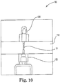
- Figure 10 is a scanning electron microscope image 180 illustrating an example of a test sample 31 mounted across pulling gap 118 between sample mounting areas 120 and 122 of PTP transformer 100, according to one embodiment.
- mounted test sample 31 is a silicon nanowire having a length of 20 ⁇ m and a diameter of 250 nm.
- a FEI Strata 235 Dual-Beam Focused Ion Beam (FIB) system by FEI Company was used to mount the sample.
- the mounting process includes:
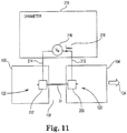
- FIG. 11 is a block and schematic diagram generally illustrating PTP transformer 100, according to one embodiment.
- a first sample contact 200 is formed (e.g. via metal deposition and photolithographic patterning processes) in sample mounting area 120 of moveable structure 104, and a second sample contact 202 is formed in sample mounting area 122 of stationary structure 102.
- An external ohmmeter 210 is respectively coupled to first and second sample contacts 200, 202 via leads 212 and 214 (e.g. at least partially comprising conductive traces on stationary and moveable structures 102, 104, as illustrated by Figures 13 and 14 below).
- Test sample 31 is connected to contacts 200, 202, such as by welding processes as described above (e.g. via deposition of gold or other suitable electrically conductive material), across pulling gap 118.
- a voltmeter 216 of ohmmeter 210 provides a sense current 218 which passes through test sample 31 via contacts 200, 202 and leads 212, 214 to measure an electrical resistance of test sample 31 during the tensile testing procedure.
- Such a configuration is generally referred to as a two-point measurement. It is noted that, according to such a two-point measurement, the ohmmeter measures not only the resistance across test sample 31, but also that of contacts 200, 202 and leads 212, 214.
- FIG 12 is a block and schematic diagram generally illustrating a further embodiment of PTP transformer 100.
- PTP transformer 100 includes a further contact 204 formed in sample mounting area 120 of moveable structure 104 and a further contact 206 formed in sample mounted area 122 of stationary structure 102.
- Test sample 31 is connected to contacts 200, 204 of moveable structure 104 and to contacts 202, 206, across pulling gap 118.
- external ohmmeter 210 is respectively coupled to sample contacts 204 and 206 via leads 220 and 222.
- external ohmmeter 210 is respectively coupled to first and second sample contacts 200, 202 via leads 212 and 214 and provides a sense current 218 via voltmeter 216.
- a power supply 224 of ohmmeter 210 is coupled to and provides a test current 226 through sample 31 via contacts 204 and 206.
- Such a configuration is generally referred to as a four-point measurement.
- the four-point measurement scheme employs a very low magnitude sense current 218 relative to test current 226 so that a voltage drop resulting from sense current 218 can be considered negligible.
- the resistance measured by ohmmeter 210 can be assumed to represent the resistance of only sample 31.
- FIG 13 is a perspective view illustrating PTP transformer 100 of Figure 12 , according to one embodiment.
- stationary structure 102 includes external contacts 230, 232, 234, and 236, and ground contacts 240, 242, and 244.
- External contacts 230 and 234 are respectively connected to sample contacts 200 and 204 of moveable structure 104 via conductive traces 250 and 254 which are respectively routed across a top surface of springs 107 and 108.
- External contacts 232 and 236 are respectively connected to sample contacts 202 and 206 via conductive traces 252 and 256.
- external leads of voltmeter 216 and power supply 224 are respectively coupled to external contacts 230, 234 and external contacts 232, 236 of stationary structure 102 of PTP transformer 100.
- External contacts 230, 232, 234, 236 and leads 250, 252, 254, 256 are electrically isolated from device layer 140 by a silicon dioxide layer between device layer 140 and the metal electrodes.
- Ground contacts 240 and 244 are connected to stationary structure 102 and to moveable structure 104 via springs 105 and 106, respectively, and ground contact 244 is connected to stationary structure 102. It is noted that a large portion of a surface of device layer 140 of PTP transformer 100 (see Figure 6 ) comprises a ground electrode, which helps to eliminate electron charge on PTP transformer 100 and thereby reduces error which might otherwise be caused by an undesirable electrostatic interaction between PTP transformer 100 and a tip of displaceable electrode 34 of EM transducer 32 (see Figure 1 ). Such a ground connection and resulting electrical discharge is especially important for in-situ electron microscopy tests (e.g. transmission electron microscopy (TEM) and/or scanning electron microscopy (SEM)) which require removing the tip-device attraction resulting from the electrical potential between the two.
- TEM transmission electron microscopy
- SEM scanning electron microscopy
- Figure 14 is a microscope image 250 of fabricated PTP transformer 100 as illustrated by Figures 12 and 13 above.
- pulling gap 118 has a width of approximately 4 ⁇ m.
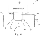
- FIG. 15 is a block and schematic diagram generally illustrating PTP transformer 100, according to one embodiment.
- a first resistive heater 260 is formed in sample mounting area 120 of moveable structure 104, and a second resistive heater 262 is formed in sample mounting area 122 of stationary structure 102.
- Resistive heaters 260 and 262 are electrically connected to a heating controller 264 via leads 266 and 268, respectively, wherein leads 266 and 268 are similar to leads/contacts described above by with respect to Figure 13 (e.g. external contacts 230, 232 and conductive traces 250, 252).
- Test sample 31 is coupled at each end proximate to resistive heaters 260, 262 and spans pulling gap 118.
- test sample 31 is heated by heating controller 264 via heaters 260, 262.
- test sample is mechanically characterized by applying a pushing force to moveable structure 104 via an actuator, such as displaceable electrode 34 of EM transducer 32 (see Figure 1 ).
- an actuator such as displaceable electrode 34 of EM transducer 32 (see Figure 1 ).
- a temperature sensor can be integrated with resistive heaters 260, 262 so that a temperature of test sample 31 can be monitored by heating controller 264 during a tensile testing procedure.
- both ohmmeter 210 and heating controller 264 may comprise stand-alone devices separately coupled to PTP transformer 100, or may be incorporated as part of controller 50 of nanomechanical test system 30 (see Figure 1 ).
- PTP linear mechanical transformer 100 for tensile testing of micrometer to nanometer scale structures.
- PTP linear mechanical transformer 100 converts a pushing force into pulling force by employing sample mounting areas 120 and 122 which are positioned on opposite sides of pulling gap 118 formed by stationary structure 102 and movable structure 104.
- sample mounting areas 120 and 122 which are positioned on opposite sides of pulling gap 118 formed by stationary structure 102 and movable structure 104.
- movable structure 104 aligns a pushing force and the resulting pulling force along a same force axis, such as along centerline 112 of PTP transformer 100.
- moveable structure 104 is coupled to stationary structure 102 via at least one spring, such as springs 105-108, which are configured to provide moveable structure 104 with a higher stiffness to the lateral and vertical directions 152, 154 as compared to tensile extension direction 124.
- springs 105-108 are configured to provide moveable structure 104 with a higher stiffness to the lateral and vertical directions 152, 154 as compared to tensile extension direction 124.
- the alignment of the pushing and pulling forces, and the stiffness characteristics of moveable structure 104 reduce undesirable effects that lateral and vertical direction forces may otherwise have on the tensile testing process.
- PTP transformer 100 can be used for in-situ electron microscopy tensile testing and, by adding conductor traces and heating elements, can also be employed for performing electromechanical and thermal-mechanical tensile testing.
- MEMS based PTP transformer 100 can serve as an accurate force calibrator for any device which requires a stiffness calibration or force calibration, such as electromechanical transducers, for example.
- a device to be calibrated can be pushed against moveable structure 104 of PTP transformer 100, and based on the resulting displacement and known stiffness of moveable structure 104, the force exerted by the device to be calibrated can be estimated.
- PTP transformer 100 offers the following advantages: (1) a large linear relationship between displacement and force; (2) high structural stability (e.g. stiffness) and one-dimensional movement; (3) a relatively large physical dimension which enables in-situ force calibration, even under optical microscopes; (4) a stiffness which can be designed to match specific stiffness requirements and (5) low-cost fabrication.
- MEMS based PTP transformer 100 can serve as a very high accuracy and resolution strain sensor which is particularly useful for measuring strain after failure of a test sample.
- a force axis e.g. centerline 112
- MEMS based PTP transformer 100 can be employed to measure a relationship between an attraction force and distance between the fractured surfaces of a failed test sample. Because of the single axis movement of moveable structure 104, the fractures surfaces will match to one another after retracting of the external pushing force. A resolution is determined by EM transducer 32.
- MEMS based PTP transformer 100 can effectively protect a test sample from potential pre-test failure resulting from a power-on of the actuation device (e.g. EM transducer 32).
- the actuation device e.g. EM transducer 32
- the actuation device is accompanied by some vibration.
- the vibration is comparatively small and is not of concern.
- nanomechanical testing such vibration may be sufficient to cause failure of the test sample.
- MEMS based PTP transformer 100 simplifies sample preparation from a 3-dimensional process to a one-dimensional process because both sides of pulling gap 118 are on a same plane so that the test sample needs only to be aligned along an axis perpendicular to pulling gap 118.
- the springs of MEMS based PTP transformer 100 such as springs 105-108, act as energy buffers upon failure or yield of test sample 31 and ensure the stability of the test system.
- MEMS based PTP transformer 100 has a much higher natural frequency (e.g. greater than ten times) than the actuation and sensing devices (e.g. EM transducer 32), the resolution of the actuation and sensing devices is not sacrificed.
Claims (12)
- Dispositif microélectromécanique pour tester des échantillons de matière à l'échelle micro-nanoscopique comprenant :
un transformateur mécanique pousser-pour-tirer (100), comprenant :une première structure (102) ; etune seconde structure (104) disposée par rapport à la première structure (102) pour former un espace de tirage (118) entre celles-ci, la seconde structure (104) couplée à la première structure (102) par au moins un élément élastique (105, 106) de sorte que lorsqu'une force de poussée externe est appliquée à et pousse la seconde structure (104) vers la première structure (102) dans une direction d'extension par traction (124) l'au moins un élément élastique (105, 106) se comprime et une largeur de l'espace de tirage (118) augmente pour appliquer une force de traction à un échantillon de test (31) monté dans l'espace de tirage (118) entre une première zone de montage d'échantillon (122) sur la première structure (102) et une seconde zone de montage d'échantillon (120) sur la seconde structure (104). - Dispositif microélectromécanique selon la revendication 1, dans lequel l'espace de tirage (118) croise un axe de force de poussée (112) le long de ladite direction d'extension par traction le long de laquelle la force de poussée est appliquée.
- Dispositif microélectromécanique selon la revendication 2, dans lequel l'axe de force de poussée (112) comprend une ligne centrale du transformateur pousser-pour-tirer.
- Dispositif microélectromécanique selon la revendication 1, incluant une paire d'espaces de poussée (114, 116) entre les première (102) et seconde (104) structures, l'espace de tirage (118) positionné entre la paire d'espaces de poussée (114, 116), dans lequel une largeur de chacun des espaces de poussée (114, 116) de la paire d'espaces de poussée (114, 116) diminue lorsque la force de poussée est appliquée à et pousse la seconde structure (104) dans la direction d'extension par traction (124).
- Dispositif microélectromécanique selon la revendication 1, dans lequel la paire d'espaces de poussée (114, 116) et l'espace de traction (118) croisent un axe de force de poussée le long de ladite direction d'extension par traction le long de laquelle la force de poussée est appliquée.
- Dispositif microélectromécanique selon la revendication 5, dans lequel les première et seconde zones de montage d'échantillon (122, 120) sont disposées sur un axe de force de poussée le long de ladite direction d'extension par traction le long de laquelle la force de poussée est appliquée.
- Dispositif microélectromécanique selon la revendication 5, dans lequel une première résistance chauffante (260) est disposée au niveau de la première zone de montage d'échantillon (122) et une seconde résistance chauffante (262) est disposée au niveau de la seconde zone de montage d'échantillon (120), les première et seconde résistances chauffantes (260, 262) configurées pour chauffer l'échantillon de test (31) à une température souhaitée.
- Dispositif microélectromécanique selon la revendication 1, dans lequel l'au moins un élément élastique (105, 106) est configuré avec une rigidité pour permettre le mouvement de la seconde structure (104) dans la direction d'extension par traction (124) et pour résister au mouvement de la seconde structure (104) dans des directions autres que la direction d'extension par traction (124).
- Procédé de test d'échantillons de matière à l'échelle micro-nanoscopique comprenant :le montage d'un échantillon de matière à l'échelle micro-nanoscopique (31) dans l'espace de tirage (118) entre la première structure (102) et la seconde structure (104) du dispositif microélectromécanique selon la revendication 1 ; etla poussée de la seconde structure (104) avec une force de poussée externe qui comprime l'au moins un élément élastique (105, 106) et augmente une largeur de l'espace de tirage (118) de façon à appliquer une force de traction à l'échantillon de matière (31).
- Procédé selon la revendication 9, incluant la mesure d'une résistance électrique de l'échantillon de matière (31) lorsque la force de poussée pousse la seconde structure (104).
- Procédé selon la revendication 9, incluant le chauffage de l'échantillon de matière (31) à une température souhaitée en utilisant une première résistance chauffante (260) au niveau de la première zone de montage d'échantillon (122) et une seconde résistance chauffante (262) disposée au niveau de la seconde zone de montage d'échantillon (120) après avoir été monté dans l'espace de tirage (118) et avant de pousser la seconde structure (104).
- Procédé selon la revendication 9, incluant la mesure de la force de poussée et l'augmentation de la largeur de l'espace de tirage (118) et la détermination d'une courbe force/déplacement pour l'échantillon de matière (31) sur la base des mesures.
Applications Claiming Priority (3)
| Application Number | Priority Date | Filing Date | Title |
|---|---|---|---|
| US10345608P | 2008-10-07 | 2008-10-07 | |
| PCT/US2009/059881 WO2010042645A2 (fr) | 2008-10-07 | 2009-10-07 | Système d’essai micro/nano-mécanique comportant un support pour essai de traction muni d’un transformateur pousser-tirer |
| EP09793343.6A EP2349913B1 (fr) | 2008-10-07 | 2009-10-07 | Système d'essai micro/nano-mécanique comportant un support pour essai de traction muni d'un transformateur pousser-tirer |
Related Parent Applications (2)
| Application Number | Title | Priority Date | Filing Date |
|---|---|---|---|
| EP09793343.6A Division EP2349913B1 (fr) | 2008-10-07 | 2009-10-07 | Système d'essai micro/nano-mécanique comportant un support pour essai de traction muni d'un transformateur pousser-tirer |
| EP09793343.6A Division-Into EP2349913B1 (fr) | 2008-10-07 | 2009-10-07 | Système d'essai micro/nano-mécanique comportant un support pour essai de traction muni d'un transformateur pousser-tirer |
Publications (2)
| Publication Number | Publication Date |
|---|---|
| EP2790004A1 EP2790004A1 (fr) | 2014-10-15 |
| EP2790004B1 true EP2790004B1 (fr) | 2019-04-17 |
Family
ID=41818741
Family Applications (2)
| Application Number | Title | Priority Date | Filing Date |
|---|---|---|---|
| EP14001610.6A Active EP2790004B1 (fr) | 2008-10-07 | 2009-10-07 | Système d'essai micro/nano-mécanique comportant un support d'essai de traction avec transformateur de poussoir/tirage |
| EP09793343.6A Active EP2349913B1 (fr) | 2008-10-07 | 2009-10-07 | Système d'essai micro/nano-mécanique comportant un support pour essai de traction muni d'un transformateur pousser-tirer |
Family Applications After (1)
| Application Number | Title | Priority Date | Filing Date |
|---|---|---|---|
| EP09793343.6A Active EP2349913B1 (fr) | 2008-10-07 | 2009-10-07 | Système d'essai micro/nano-mécanique comportant un support pour essai de traction muni d'un transformateur pousser-tirer |
Country Status (3)
| Country | Link |
|---|---|
| US (2) | US8434370B2 (fr) |
| EP (2) | EP2790004B1 (fr) |
| WO (1) | WO2010042645A2 (fr) |
Families Citing this family (27)
| Publication number | Priority date | Publication date | Assignee | Title |
|---|---|---|---|---|
| US10842653B2 (en) | 2007-09-19 | 2020-11-24 | Ability Dynamics, Llc | Vacuum system for a prosthetic foot |
| EP2480925B1 (fr) * | 2009-09-21 | 2018-11-28 | Femtotools AG | Système de caractérisation mécanique de matériaux et d'échantillons biologiques dans une plage de forces de l'ordre du sous-millinewton |
| JP5826760B2 (ja) | 2009-11-27 | 2015-12-02 | ハイジトロン, インク.Hysitron, Inc. | ミクロ電気機械ヒータ |
| US8631687B2 (en) | 2010-04-19 | 2014-01-21 | Hysitron, Inc. | Indenter assembly |
| US9194727B2 (en) * | 2010-11-24 | 2015-11-24 | Hysitron, Inc. | Mechanical testing instruments including onboard data |
| JP5735185B2 (ja) | 2011-11-14 | 2015-06-17 | ハイジトロン, インク.Hysitron, Inc. | プローブ先端加熱アセンブリ |
| US9804072B2 (en) | 2011-11-28 | 2017-10-31 | Hysitron, Inc. | High temperature heating system |
| EP2861934B1 (fr) * | 2012-06-13 | 2017-05-03 | Hysitron, Inc. | Ensemble de création de conditions ambiantes destiné à être utilisé dans des essais mécaniques à l'échelle micrométrique ou nanométrique |
| US20150273600A1 (en) * | 2012-10-25 | 2015-10-01 | Applied Materials, Inc. | Electro discharge machining system and method of operation thereof |
| US9341663B2 (en) * | 2013-11-26 | 2016-05-17 | Freescale Semiconductor, Inc. | MEMS device positioning apparatus, test system, and test method |
| US9588327B2 (en) * | 2013-12-12 | 2017-03-07 | The Board Of Trustees Of The University Of Illinois | Nanoindenter multimodal microscope objective for mechanobiology |
| CN103884585B (zh) * | 2014-03-23 | 2016-08-17 | 北京工业大学 | 一种透射电镜用基于形状记忆效应的原位单轴拉伸变形装置 |
| EP2960637B1 (fr) * | 2014-06-24 | 2019-08-28 | Femtotools AG | Conception et interface d'un capteur de force à balayage microfabriqué pour une détection combinée de force et de position |
| CN104634660B (zh) * | 2015-02-04 | 2017-05-10 | 北京工业大学 | 透射电镜中原位双倾单轴拉伸纳米线、二维层状薄膜装置及方法 |
| CN104764660A (zh) * | 2015-03-29 | 2015-07-08 | 北京工业大学 | 一种扫描/透射电子显微镜用热驱动单轴拉伸/压缩变形装置 |
| CN105223213B (zh) * | 2015-09-28 | 2017-12-15 | 北京工业大学 | 一种透射电镜双倾原位纳米压痕平台 |
| WO2017139384A1 (fr) * | 2016-02-09 | 2017-08-17 | The Board Of Regents Of The University Of Texas System | Coagulomètre sanguin et procédé |
| JP6209635B2 (ja) * | 2016-03-15 | 2017-10-04 | 日新製鋼株式会社 | 金属屋根材の強度試験方法、強度試験設備及び仮想強度試験プログラム |
| KR101947155B1 (ko) * | 2017-08-25 | 2019-02-12 | 울산과학기술원 | 그래핀 인장 시험 방법 |
| US10330543B1 (en) * | 2018-04-03 | 2019-06-25 | Avangrid Renewables, LLC | Measurement of tension in securing members |
| US11557456B2 (en) * | 2018-09-14 | 2023-01-17 | University Of Connecticut | Real-time direct measurement of mechanical properties in-situ of scanning beam microscope |
| CN110261221B (zh) * | 2019-05-22 | 2023-12-29 | 北京工业大学 | 一种原位拉伸装置及其制备方法 |
| US11668633B2 (en) * | 2020-04-21 | 2023-06-06 | The Boeing Company | Compressive creep flow determination in fluids |
| CN112975282B (zh) * | 2021-02-09 | 2022-02-01 | 芜湖造船厂有限公司 | 用于确定夏比冲击试验试样缺口加工位置的方法 |
| CN113138125B (zh) * | 2021-04-21 | 2023-03-14 | 北京工业大学 | 原位双倾单轴拉伸纳米线装置及其制作方法 |
| CN114813383B (zh) * | 2022-05-20 | 2023-06-06 | 清华大学 | 原位拉伸装置及其制作方法 |
| CN115683845A (zh) * | 2022-10-17 | 2023-02-03 | 哈尔滨工业大学 | 原位力学测试用推-拉微器械 |
Family Cites Families (16)
| Publication number | Priority date | Publication date | Assignee | Title |
|---|---|---|---|---|
| US5060519A (en) | 1988-02-18 | 1991-10-29 | Tokkyo Kiki Kabushiki Kaisha | Active control precision damping table |
| US6199874B1 (en) * | 1993-05-26 | 2001-03-13 | Cornell Research Foundation Inc. | Microelectromechanical accelerometer for automotive applications |
| US5553486A (en) | 1993-10-01 | 1996-09-10 | Hysitron Incorporated | Apparatus for microindentation hardness testing and surface imaging incorporating a multi-plate capacitor system |
| US5661235A (en) | 1993-10-01 | 1997-08-26 | Hysitron Incorporated | Multi-dimensional capacitive transducer |
| US6466678B1 (en) | 1994-11-30 | 2002-10-15 | Etymotic Research, Inc. | Hearing aid having digital damping |
| US6606913B1 (en) | 1998-11-06 | 2003-08-19 | Wisconsin Alumni Research Foundation | Micromachined strain sensor |
| US20010013574A1 (en) | 1998-11-10 | 2001-08-16 | Oden L. Warren | Intermittent contact imaging under force-feedback control |
| US6817255B2 (en) | 2001-09-12 | 2004-11-16 | The Board Of Trustees Of The University Of Illinois | Apparatus and method for testing of microscale to nanoscale thin films |
| US6891657B2 (en) | 2003-05-20 | 2005-05-10 | Texas Instruments Incorporated | Damped control of a micromechanical device |
| US6985278B2 (en) | 2003-05-20 | 2006-01-10 | Texas Instruments Incorporated | Damped control of a micromechanical device |
| US7165445B2 (en) | 2003-08-25 | 2007-01-23 | Asylum Research Corporation | Digital control of quality factor in resonant systems including cantilever based instruments |
| US8770050B2 (en) * | 2006-03-17 | 2014-07-08 | Jason Vaughn Clark | Method of measuring micro- and nano-scale properties |
| US7681459B1 (en) * | 2006-04-12 | 2010-03-23 | Hysitron, Incorporated | Multi-scale & three-axis sensing tensile testing apparatus |
| EP2029996A2 (fr) * | 2006-06-02 | 2009-03-04 | Mts Systems Corporation | Mesure des propriétés de spécimens minces basés sur des données de déplacement de forces acquises de manière expérimentale |
| US7878071B2 (en) * | 2006-12-22 | 2011-02-01 | California Institute Of Technology | Nanoindenter tip for uniaxial tension and compression testing |
| US7752916B2 (en) * | 2007-08-31 | 2010-07-13 | The Board Of Trustees Of The University Of Illinois | Apparatus and method for material testing of microscale and nanoscale samples |
-
2009
- 2009-10-07 EP EP14001610.6A patent/EP2790004B1/fr active Active
- 2009-10-07 EP EP09793343.6A patent/EP2349913B1/fr active Active
- 2009-10-07 WO PCT/US2009/059881 patent/WO2010042645A2/fr active Application Filing
- 2009-10-07 US US12/575,368 patent/US8434370B2/en active Active
-
2013
- 2013-05-07 US US13/888,959 patent/US8789425B2/en active Active
Non-Patent Citations (1)
| Title |
|---|
| None * |
Also Published As
| Publication number | Publication date |
|---|---|
| EP2790004A1 (fr) | 2014-10-15 |
| WO2010042645A2 (fr) | 2010-04-15 |
| US8789425B2 (en) | 2014-07-29 |
| US20130247682A1 (en) | 2013-09-26 |
| EP2349913A2 (fr) | 2011-08-03 |
| EP2349913B1 (fr) | 2017-09-20 |
| US20100095780A1 (en) | 2010-04-22 |
| US8434370B2 (en) | 2013-05-07 |
| WO2010042645A3 (fr) | 2010-08-19 |
Similar Documents
| Publication | Publication Date | Title |
|---|---|---|
| EP2790004B1 (fr) | Système d'essai micro/nano-mécanique comportant un support d'essai de traction avec transformateur de poussoir/tirage | |
| JP6195948B2 (ja) | コムドライブを備えた2次元memsトライボメータ | |
| EP2310830B1 (fr) | Entraînement de type peigne micro-usiné pour nanoindentation quantitative | |
| EP1829050B1 (fr) | Appareil de balayage pour microscopie a sonde | |
| EP2780689B1 (fr) | Ensemble de chauffage de pointe de sonde | |
| US9759641B2 (en) | Micro electro-mechanical heater | |
| US20060186874A1 (en) | System and method for mechanical testing of freestanding microscale to nanoscale thin films | |
| JP2013525798A5 (fr) | ||
| Lu et al. | A multi-step method for in situ mechanical characterization of 1-D nanostructures using a novel micromechanical device | |
| JP2013512545A5 (fr) | ||
| US6424165B1 (en) | Electrostatic apparatus for measurement of microfracture strength | |
| US20080011046A1 (en) | Displacement Method for Determining the Spring Constant of Scanning Probe Microscope Cantileers using MEMS Actuators | |
| EP2926111B1 (fr) | Entraînement par peigne micro-usiné pour nano-indentation quantitative | |
| GB2419952A (en) | Atomic force microscope (AFM) lateral force calibration | |
| JP3675406B2 (ja) | マイクロ材料試験装置及びこれによる力学特性評価方法 | |
| Desai et al. | Design and fabrication of a novel MEMS device for high resolution force and displacement measurement | |
| Li | Development of Microelectromechanical Systems for Advanced Nanomechanical Characterization | |
| Ganesan et al. | In situ mechanical characterization of one dimensional nanoscale building blocks using novel microfabricated devices |
Legal Events
| Date | Code | Title | Description |
|---|---|---|---|
| PUAI | Public reference made under article 153(3) epc to a published international application that has entered the european phase |
Free format text: ORIGINAL CODE: 0009012 |
|
| 17P | Request for examination filed |
Effective date: 20140507 |
|
| AC | Divisional application: reference to earlier application |
Ref document number: 2349913 Country of ref document: EP Kind code of ref document: P |
|
| AK | Designated contracting states |
Kind code of ref document: A1 Designated state(s): AT BE BG CH CY CZ DE DK EE ES FI FR GB GR HR HU IE IS IT LI LT LU LV MC MK MT NL NO PL PT RO SE SI SK SM TR |
|
| RIN1 | Information on inventor provided before grant (corrected) |
Inventor name: OH, YUNJE Inventor name: ASIF, SYED AMANULA SYED Inventor name: SHAN, ZHIWEI Inventor name: CYRANKOWSKI, EDWARD J. |
|
| R17P | Request for examination filed (corrected) |
Effective date: 20150415 |
|
| RBV | Designated contracting states (corrected) |
Designated state(s): AT BE BG CH CY CZ DE DK EE ES FI FR GB GR HR HU IE IS IT LI LT LU LV MC MK MT NL NO PL PT RO SE SI SK SM TR |
|
| STAA | Information on the status of an ep patent application or granted ep patent |
Free format text: STATUS: EXAMINATION IS IN PROGRESS |
|
| 17Q | First examination report despatched |
Effective date: 20170323 |
|
| GRAP | Despatch of communication of intention to grant a patent |
Free format text: ORIGINAL CODE: EPIDOSNIGR1 |
|
| STAA | Information on the status of an ep patent application or granted ep patent |
Free format text: STATUS: GRANT OF PATENT IS INTENDED |
|
| INTG | Intention to grant announced |
Effective date: 20181002 |
|
| RAP1 | Party data changed (applicant data changed or rights of an application transferred) |
Owner name: BRUKER NANO, INC. |
|
| GRAS | Grant fee paid |
Free format text: ORIGINAL CODE: EPIDOSNIGR3 |
|
| GRAA | (expected) grant |
Free format text: ORIGINAL CODE: 0009210 |
|
| STAA | Information on the status of an ep patent application or granted ep patent |
Free format text: STATUS: THE PATENT HAS BEEN GRANTED |
|
| AC | Divisional application: reference to earlier application |
Ref document number: 2349913 Country of ref document: EP Kind code of ref document: P |
|
| AK | Designated contracting states |
Kind code of ref document: B1 Designated state(s): AT BE BG CH CY CZ DE DK EE ES FI FR GB GR HR HU IE IS IT LI LT LU LV MC MK MT NL NO PL PT RO SE SI SK SM TR |
|
| REG | Reference to a national code |
Ref country code: GB Ref legal event code: FG4D |
|
| REG | Reference to a national code |
Ref country code: CH Ref legal event code: EP |
|
| REG | Reference to a national code |
Ref country code: DE Ref legal event code: R096 Ref document number: 602009057975 Country of ref document: DE |
|
| REG | Reference to a national code |
Ref country code: AT Ref legal event code: REF Ref document number: 1122092 Country of ref document: AT Kind code of ref document: T Effective date: 20190515 Ref country code: IE Ref legal event code: FG4D |
|
| REG | Reference to a national code |
Ref country code: CH Ref legal event code: NV Representative=s name: RENTSCH PARTNER AG, CH |
|
| REG | Reference to a national code |
Ref country code: NL Ref legal event code: MP Effective date: 20190417 |
|
| REG | Reference to a national code |
Ref country code: LT Ref legal event code: MG4D |
|
| PG25 | Lapsed in a contracting state [announced via postgrant information from national office to epo] |
Ref country code: NL Free format text: LAPSE BECAUSE OF FAILURE TO SUBMIT A TRANSLATION OF THE DESCRIPTION OR TO PAY THE FEE WITHIN THE PRESCRIBED TIME-LIMIT Effective date: 20190417 |
|
| PG25 | Lapsed in a contracting state [announced via postgrant information from national office to epo] |
Ref country code: NO Free format text: LAPSE BECAUSE OF FAILURE TO SUBMIT A TRANSLATION OF THE DESCRIPTION OR TO PAY THE FEE WITHIN THE PRESCRIBED TIME-LIMIT Effective date: 20190717 Ref country code: FI Free format text: LAPSE BECAUSE OF FAILURE TO SUBMIT A TRANSLATION OF THE DESCRIPTION OR TO PAY THE FEE WITHIN THE PRESCRIBED TIME-LIMIT Effective date: 20190417 Ref country code: PT Free format text: LAPSE BECAUSE OF FAILURE TO SUBMIT A TRANSLATION OF THE DESCRIPTION OR TO PAY THE FEE WITHIN THE PRESCRIBED TIME-LIMIT Effective date: 20190817 Ref country code: ES Free format text: LAPSE BECAUSE OF FAILURE TO SUBMIT A TRANSLATION OF THE DESCRIPTION OR TO PAY THE FEE WITHIN THE PRESCRIBED TIME-LIMIT Effective date: 20190417 Ref country code: SE Free format text: LAPSE BECAUSE OF FAILURE TO SUBMIT A TRANSLATION OF THE DESCRIPTION OR TO PAY THE FEE WITHIN THE PRESCRIBED TIME-LIMIT Effective date: 20190417 Ref country code: LT Free format text: LAPSE BECAUSE OF FAILURE TO SUBMIT A TRANSLATION OF THE DESCRIPTION OR TO PAY THE FEE WITHIN THE PRESCRIBED TIME-LIMIT Effective date: 20190417 Ref country code: HR Free format text: LAPSE BECAUSE OF FAILURE TO SUBMIT A TRANSLATION OF THE DESCRIPTION OR TO PAY THE FEE WITHIN THE PRESCRIBED TIME-LIMIT Effective date: 20190417 |
|
| PG25 | Lapsed in a contracting state [announced via postgrant information from national office to epo] |
Ref country code: PL Free format text: LAPSE BECAUSE OF FAILURE TO SUBMIT A TRANSLATION OF THE DESCRIPTION OR TO PAY THE FEE WITHIN THE PRESCRIBED TIME-LIMIT Effective date: 20190417 Ref country code: GR Free format text: LAPSE BECAUSE OF FAILURE TO SUBMIT A TRANSLATION OF THE DESCRIPTION OR TO PAY THE FEE WITHIN THE PRESCRIBED TIME-LIMIT Effective date: 20190718 Ref country code: BG Free format text: LAPSE BECAUSE OF FAILURE TO SUBMIT A TRANSLATION OF THE DESCRIPTION OR TO PAY THE FEE WITHIN THE PRESCRIBED TIME-LIMIT Effective date: 20190717 Ref country code: LV Free format text: LAPSE BECAUSE OF FAILURE TO SUBMIT A TRANSLATION OF THE DESCRIPTION OR TO PAY THE FEE WITHIN THE PRESCRIBED TIME-LIMIT Effective date: 20190417 |
|
| REG | Reference to a national code |
Ref country code: AT Ref legal event code: MK05 Ref document number: 1122092 Country of ref document: AT Kind code of ref document: T Effective date: 20190417 |
|
| PG25 | Lapsed in a contracting state [announced via postgrant information from national office to epo] |
Ref country code: IS Free format text: LAPSE BECAUSE OF FAILURE TO SUBMIT A TRANSLATION OF THE DESCRIPTION OR TO PAY THE FEE WITHIN THE PRESCRIBED TIME-LIMIT Effective date: 20190817 |
|
| REG | Reference to a national code |
Ref country code: DE Ref legal event code: R097 Ref document number: 602009057975 Country of ref document: DE |
|
| PG25 | Lapsed in a contracting state [announced via postgrant information from national office to epo] |
Ref country code: CZ Free format text: LAPSE BECAUSE OF FAILURE TO SUBMIT A TRANSLATION OF THE DESCRIPTION OR TO PAY THE FEE WITHIN THE PRESCRIBED TIME-LIMIT Effective date: 20190417 Ref country code: AT Free format text: LAPSE BECAUSE OF FAILURE TO SUBMIT A TRANSLATION OF THE DESCRIPTION OR TO PAY THE FEE WITHIN THE PRESCRIBED TIME-LIMIT Effective date: 20190417 Ref country code: EE Free format text: LAPSE BECAUSE OF FAILURE TO SUBMIT A TRANSLATION OF THE DESCRIPTION OR TO PAY THE FEE WITHIN THE PRESCRIBED TIME-LIMIT Effective date: 20190417 Ref country code: RO Free format text: LAPSE BECAUSE OF FAILURE TO SUBMIT A TRANSLATION OF THE DESCRIPTION OR TO PAY THE FEE WITHIN THE PRESCRIBED TIME-LIMIT Effective date: 20190417 Ref country code: DK Free format text: LAPSE BECAUSE OF FAILURE TO SUBMIT A TRANSLATION OF THE DESCRIPTION OR TO PAY THE FEE WITHIN THE PRESCRIBED TIME-LIMIT Effective date: 20190417 Ref country code: SK Free format text: LAPSE BECAUSE OF FAILURE TO SUBMIT A TRANSLATION OF THE DESCRIPTION OR TO PAY THE FEE WITHIN THE PRESCRIBED TIME-LIMIT Effective date: 20190417 |
|
| PLBE | No opposition filed within time limit |
Free format text: ORIGINAL CODE: 0009261 |
|
| STAA | Information on the status of an ep patent application or granted ep patent |
Free format text: STATUS: NO OPPOSITION FILED WITHIN TIME LIMIT |
|
| PG25 | Lapsed in a contracting state [announced via postgrant information from national office to epo] |
Ref country code: SM Free format text: LAPSE BECAUSE OF FAILURE TO SUBMIT A TRANSLATION OF THE DESCRIPTION OR TO PAY THE FEE WITHIN THE PRESCRIBED TIME-LIMIT Effective date: 20190417 Ref country code: IT Free format text: LAPSE BECAUSE OF FAILURE TO SUBMIT A TRANSLATION OF THE DESCRIPTION OR TO PAY THE FEE WITHIN THE PRESCRIBED TIME-LIMIT Effective date: 20190417 |
|
| 26N | No opposition filed |
Effective date: 20200120 |
|
| PG25 | Lapsed in a contracting state [announced via postgrant information from national office to epo] |
Ref country code: TR Free format text: LAPSE BECAUSE OF FAILURE TO SUBMIT A TRANSLATION OF THE DESCRIPTION OR TO PAY THE FEE WITHIN THE PRESCRIBED TIME-LIMIT Effective date: 20190417 |
|
| PG25 | Lapsed in a contracting state [announced via postgrant information from national office to epo] |
Ref country code: SI Free format text: LAPSE BECAUSE OF FAILURE TO SUBMIT A TRANSLATION OF THE DESCRIPTION OR TO PAY THE FEE WITHIN THE PRESCRIBED TIME-LIMIT Effective date: 20190417 Ref country code: MC Free format text: LAPSE BECAUSE OF FAILURE TO SUBMIT A TRANSLATION OF THE DESCRIPTION OR TO PAY THE FEE WITHIN THE PRESCRIBED TIME-LIMIT Effective date: 20190417 |
|
| PG25 | Lapsed in a contracting state [announced via postgrant information from national office to epo] |
Ref country code: LU Free format text: LAPSE BECAUSE OF NON-PAYMENT OF DUE FEES Effective date: 20191007 |
|
| REG | Reference to a national code |
Ref country code: BE Ref legal event code: MM Effective date: 20191031 |
|
| PG25 | Lapsed in a contracting state [announced via postgrant information from national office to epo] |
Ref country code: BE Free format text: LAPSE BECAUSE OF NON-PAYMENT OF DUE FEES Effective date: 20191031 |
|
| PG25 | Lapsed in a contracting state [announced via postgrant information from national office to epo] |
Ref country code: IE Free format text: LAPSE BECAUSE OF NON-PAYMENT OF DUE FEES Effective date: 20191007 |
|
| PG25 | Lapsed in a contracting state [announced via postgrant information from national office to epo] |
Ref country code: CY Free format text: LAPSE BECAUSE OF FAILURE TO SUBMIT A TRANSLATION OF THE DESCRIPTION OR TO PAY THE FEE WITHIN THE PRESCRIBED TIME-LIMIT Effective date: 20190417 |
|
| PG25 | Lapsed in a contracting state [announced via postgrant information from national office to epo] |
Ref country code: HU Free format text: LAPSE BECAUSE OF FAILURE TO SUBMIT A TRANSLATION OF THE DESCRIPTION OR TO PAY THE FEE WITHIN THE PRESCRIBED TIME-LIMIT; INVALID AB INITIO Effective date: 20091007 Ref country code: MT Free format text: LAPSE BECAUSE OF FAILURE TO SUBMIT A TRANSLATION OF THE DESCRIPTION OR TO PAY THE FEE WITHIN THE PRESCRIBED TIME-LIMIT Effective date: 20190417 |
|
| PG25 | Lapsed in a contracting state [announced via postgrant information from national office to epo] |
Ref country code: MK Free format text: LAPSE BECAUSE OF FAILURE TO SUBMIT A TRANSLATION OF THE DESCRIPTION OR TO PAY THE FEE WITHIN THE PRESCRIBED TIME-LIMIT Effective date: 20190417 |
|
| PGFP | Annual fee paid to national office [announced via postgrant information from national office to epo] |
Ref country code: GB Payment date: 20231006 Year of fee payment: 15 |
|
| PGFP | Annual fee paid to national office [announced via postgrant information from national office to epo] |
Ref country code: FR Payment date: 20231009 Year of fee payment: 15 Ref country code: DE Payment date: 20231003 Year of fee payment: 15 Ref country code: CH Payment date: 20231102 Year of fee payment: 15 |