EP2785149A1 - Drive system of semiconductor light source, and semiconductor lighting device - Google Patents
Drive system of semiconductor light source, and semiconductor lighting device Download PDFInfo
- Publication number
- EP2785149A1 EP2785149A1 EP13800096.3A EP13800096A EP2785149A1 EP 2785149 A1 EP2785149 A1 EP 2785149A1 EP 13800096 A EP13800096 A EP 13800096A EP 2785149 A1 EP2785149 A1 EP 2785149A1
- Authority
- EP
- European Patent Office
- Prior art keywords
- coil
- light source
- semiconductor light
- transformer
- energy
- Prior art date
- Legal status (The legal status is an assumption and is not a legal conclusion. Google has not performed a legal analysis and makes no representation as to the accuracy of the status listed.)
- Granted
Links
Images



Classifications
-
- H—ELECTRICITY
- H05—ELECTRIC TECHNIQUES NOT OTHERWISE PROVIDED FOR
- H05B—ELECTRIC HEATING; ELECTRIC LIGHT SOURCES NOT OTHERWISE PROVIDED FOR; CIRCUIT ARRANGEMENTS FOR ELECTRIC LIGHT SOURCES, IN GENERAL
- H05B45/00—Circuit arrangements for operating light-emitting diodes [LED]
- H05B45/30—Driver circuits
- H05B45/37—Converter circuits
- H05B45/3725—Switched mode power supply [SMPS]
-
- G—PHYSICS
- G09—EDUCATION; CRYPTOGRAPHY; DISPLAY; ADVERTISING; SEALS
- G09G—ARRANGEMENTS OR CIRCUITS FOR CONTROL OF INDICATING DEVICES USING STATIC MEANS TO PRESENT VARIABLE INFORMATION
- G09G3/00—Control arrangements or circuits, of interest only in connection with visual indicators other than cathode-ray tubes
- G09G3/20—Control arrangements or circuits, of interest only in connection with visual indicators other than cathode-ray tubes for presentation of an assembly of a number of characters, e.g. a page, by composing the assembly by combination of individual elements arranged in a matrix no fixed position being assigned to or needed to be assigned to the individual characters or partial characters
- G09G3/34—Control arrangements or circuits, of interest only in connection with visual indicators other than cathode-ray tubes for presentation of an assembly of a number of characters, e.g. a page, by composing the assembly by combination of individual elements arranged in a matrix no fixed position being assigned to or needed to be assigned to the individual characters or partial characters by control of light from an independent source
- G09G3/3406—Control of illumination source
-
- H—ELECTRICITY
- H02—GENERATION; CONVERSION OR DISTRIBUTION OF ELECTRIC POWER
- H02M—APPARATUS FOR CONVERSION BETWEEN AC AND AC, BETWEEN AC AND DC, OR BETWEEN DC AND DC, AND FOR USE WITH MAINS OR SIMILAR POWER SUPPLY SYSTEMS; CONVERSION OF DC OR AC INPUT POWER INTO SURGE OUTPUT POWER; CONTROL OR REGULATION THEREOF
- H02M3/00—Conversion of DC power input into DC power output
- H02M3/02—Conversion of DC power input into DC power output without intermediate conversion into AC
- H02M3/04—Conversion of DC power input into DC power output without intermediate conversion into AC by static converters
- H02M3/10—Conversion of DC power input into DC power output without intermediate conversion into AC by static converters using discharge tubes with control electrode or semiconductor devices with control electrode
- H02M3/145—Conversion of DC power input into DC power output without intermediate conversion into AC by static converters using discharge tubes with control electrode or semiconductor devices with control electrode using devices of a triode or transistor type requiring continuous application of a control signal
- H02M3/155—Conversion of DC power input into DC power output without intermediate conversion into AC by static converters using discharge tubes with control electrode or semiconductor devices with control electrode using devices of a triode or transistor type requiring continuous application of a control signal using semiconductor devices only
- H02M3/156—Conversion of DC power input into DC power output without intermediate conversion into AC by static converters using discharge tubes with control electrode or semiconductor devices with control electrode using devices of a triode or transistor type requiring continuous application of a control signal using semiconductor devices only with automatic control of output voltage or current, e.g. switching regulators
-
- H—ELECTRICITY
- H05—ELECTRIC TECHNIQUES NOT OTHERWISE PROVIDED FOR
- H05B—ELECTRIC HEATING; ELECTRIC LIGHT SOURCES NOT OTHERWISE PROVIDED FOR; CIRCUIT ARRANGEMENTS FOR ELECTRIC LIGHT SOURCES, IN GENERAL
- H05B41/00—Circuit arrangements or apparatus for igniting or operating discharge lamps
- H05B41/14—Circuit arrangements
- H05B41/26—Circuit arrangements in which the lamp is fed by power derived from DC by means of a converter, e.g. by high-voltage DC
- H05B41/28—Circuit arrangements in which the lamp is fed by power derived from DC by means of a converter, e.g. by high-voltage DC using static converters
- H05B41/282—Circuit arrangements in which the lamp is fed by power derived from DC by means of a converter, e.g. by high-voltage DC using static converters with semiconductor devices
-
- H—ELECTRICITY
- H05—ELECTRIC TECHNIQUES NOT OTHERWISE PROVIDED FOR
- H05B—ELECTRIC HEATING; ELECTRIC LIGHT SOURCES NOT OTHERWISE PROVIDED FOR; CIRCUIT ARRANGEMENTS FOR ELECTRIC LIGHT SOURCES, IN GENERAL
- H05B41/00—Circuit arrangements or apparatus for igniting or operating discharge lamps
- H05B41/14—Circuit arrangements
- H05B41/26—Circuit arrangements in which the lamp is fed by power derived from DC by means of a converter, e.g. by high-voltage DC
- H05B41/28—Circuit arrangements in which the lamp is fed by power derived from DC by means of a converter, e.g. by high-voltage DC using static converters
- H05B41/282—Circuit arrangements in which the lamp is fed by power derived from DC by means of a converter, e.g. by high-voltage DC using static converters with semiconductor devices
- H05B41/2825—Circuit arrangements in which the lamp is fed by power derived from DC by means of a converter, e.g. by high-voltage DC using static converters with semiconductor devices by means of a bridge converter in the final stage
- H05B41/2827—Circuit arrangements in which the lamp is fed by power derived from DC by means of a converter, e.g. by high-voltage DC using static converters with semiconductor devices by means of a bridge converter in the final stage using specially adapted components in the load circuit, e.g. feed-back transformers, piezoelectric transformers; using specially adapted load circuit configurations
-
- Y—GENERAL TAGGING OF NEW TECHNOLOGICAL DEVELOPMENTS; GENERAL TAGGING OF CROSS-SECTIONAL TECHNOLOGIES SPANNING OVER SEVERAL SECTIONS OF THE IPC; TECHNICAL SUBJECTS COVERED BY FORMER USPC CROSS-REFERENCE ART COLLECTIONS [XRACs] AND DIGESTS
- Y02—TECHNOLOGIES OR APPLICATIONS FOR MITIGATION OR ADAPTATION AGAINST CLIMATE CHANGE
- Y02B—CLIMATE CHANGE MITIGATION TECHNOLOGIES RELATED TO BUILDINGS, e.g. HOUSING, HOUSE APPLIANCES OR RELATED END-USER APPLICATIONS
- Y02B20/00—Energy efficient lighting technologies, e.g. halogen lamps or gas discharge lamps
-
- Y—GENERAL TAGGING OF NEW TECHNOLOGICAL DEVELOPMENTS; GENERAL TAGGING OF CROSS-SECTIONAL TECHNOLOGIES SPANNING OVER SEVERAL SECTIONS OF THE IPC; TECHNICAL SUBJECTS COVERED BY FORMER USPC CROSS-REFERENCE ART COLLECTIONS [XRACs] AND DIGESTS
- Y02—TECHNOLOGIES OR APPLICATIONS FOR MITIGATION OR ADAPTATION AGAINST CLIMATE CHANGE
- Y02B—CLIMATE CHANGE MITIGATION TECHNOLOGIES RELATED TO BUILDINGS, e.g. HOUSING, HOUSE APPLIANCES OR RELATED END-USER APPLICATIONS
- Y02B20/00—Energy efficient lighting technologies, e.g. halogen lamps or gas discharge lamps
- Y02B20/30—Semiconductor lamps, e.g. solid state lamps [SSL] light emitting diodes [LED] or organic LED [OLED]
-
- Y—GENERAL TAGGING OF NEW TECHNOLOGICAL DEVELOPMENTS; GENERAL TAGGING OF CROSS-SECTIONAL TECHNOLOGIES SPANNING OVER SEVERAL SECTIONS OF THE IPC; TECHNICAL SUBJECTS COVERED BY FORMER USPC CROSS-REFERENCE ART COLLECTIONS [XRACs] AND DIGESTS
- Y10—TECHNICAL SUBJECTS COVERED BY FORMER USPC
- Y10S—TECHNICAL SUBJECTS COVERED BY FORMER USPC CROSS-REFERENCE ART COLLECTIONS [XRACs] AND DIGESTS
- Y10S315/00—Electric lamp and discharge devices: systems
- Y10S315/05—Starting and operating circuit for fluorescent lamp
-
- Y—GENERAL TAGGING OF NEW TECHNOLOGICAL DEVELOPMENTS; GENERAL TAGGING OF CROSS-SECTIONAL TECHNOLOGIES SPANNING OVER SEVERAL SECTIONS OF THE IPC; TECHNICAL SUBJECTS COVERED BY FORMER USPC CROSS-REFERENCE ART COLLECTIONS [XRACs] AND DIGESTS
- Y10—TECHNICAL SUBJECTS COVERED BY FORMER USPC
- Y10S—TECHNICAL SUBJECTS COVERED BY FORMER USPC CROSS-REFERENCE ART COLLECTIONS [XRACs] AND DIGESTS
- Y10S315/00—Electric lamp and discharge devices: systems
- Y10S315/07—Starting and control circuits for gas discharge lamp using transistors
Definitions
- the present disclosure relates to a driving system for a semiconductor light source, and more particularly to a driving system for a buck-boost semiconductor light source.
- a semiconductor light source such as LED is a light source and a display device produced by a third generation semiconductor material with lower power consumption, long lifespan, no pollution, rich colors, high controllability and other characteristics, which is a revolution in lighting sources and lighting industry.
- An electronic driving portion for LED is an indispensable component in a LED lighting product.
- a LED lighting device still has a higher price than a traditional light bulb or an energy saving lamp, and how to reduce the price of a LED lighting device has become a key-point of improving market acceptance.
- the price of the electronic driving portion plays a more important role in the total price of a LED lighting product.
- IC controller the main drawback of which is a higher price. If the IC controller is not adopted, a fly-back self-excited oscillation circuit is usually adopted, but such circuit has a low efficiency and a poor stability and only can output a narrow range of voltage.
- the present disclosure aims to provide an electronic driving circuit for a LED lighting product with a simple structure, a broader range of applications, and a low cost.
- a less number of elements are combined to form a self-excited oscillation circuit, and a buck-boost circuit is then combined to form a LED electronic driver.
- fewer elements are used to constitute an electronic driving portion for LED, which ensures a huge reduction of the number and cost of elements and a huge reduction of a percentage of the electronic driving portion in the LED lighting system, thereby the electronic driving portion has a high efficiency and is suitable to output a wide range of voltage.
- a driving system for a semiconductor light source including: a transformer including a first coil and a second coil coupled to each other, the second coil receiving an input voltage; a switching means connected to the second coil of the transformer in series and for controlling energy-storing and energy-releasing of the second coil; an outputting means connected to the second coil of the transformer in parallel and for supplying power to the semiconductor light source, wherein an induced signal is generated on the first coil of the transformer due to a coupling effect between the first coil and the second coil and is used for controlling turn-on or turn-off of the switching means.
- the driving system further includes a starting means for starting the switching means when the input signal is initially supplied.
- the switching means includes a switch and at least one discrete element, wherein the at least one discrete element is connected between the first coil and a control terminal of the switch, and the induced signal is used to control the switch via the at least one discrete element.
- the discrete elements include the elements such as resistors, capacitors, inductors opposite to an integrated circuit.
- the at least one discrete element includes a capacitive element.
- the at least one discrete element further includes a resistive element, and the capacitive element and the resistive element are connected in series.
- the starting means includes a resistive element and a unidirectional conducting element connected together in series, a connection point between the resistive element and the unidirectional conducting element is connected to the control terminal of the switch.
- a semiconductor lighting device including: a semiconductor light source as a load; a transformer including a first coil and a second coil coupled to each other, the second coil receiving an input voltage; a switching means connected to the second coil of the transformer in series and for controlling energy-storing and energy-releasing of the second coil; an outputting means connected to the second coil of the transformer in parallel and for supplying power to the semiconductor light source as the load, wherein an induced signal is generated on the first coil of the transformer due to a coupling effect between the first coil and the second coil and is used for controlling turn-on or turn-off of the switching means.
- Fig.1 is a schematic diagram of a driving system for a semiconductor light source according to an embodiment of the present disclosure.
- Vin represents an input voltage.
- the input voltage is a Direct Current (DC) input voltage, and may be a rectified DC voltage, or a rectified and filtered DC voltage.
- I represents a starting means
- II represents a transformer
- III represents a switching means
- IV represents an outputting means
- V represents a semiconductor light source as a load.
- the starting means I is used for ensuring the switching means to be in a turn-on state during a starting phase (that is, when the input signal Vin is initially supplied).
- the transformer II includes a first coil and a second coil coupled to each other, the second coil is used for receiving the input voltage and for storing or releasing energy under the control of the switching means III.
- An induced signal is generated on the first coil of the transformer due to a coupling effect between the first coil and the second coil and is used for controlling turn-on or turn-off of the switching means III.
- the outputting means is used for supplying power to the semiconductor light source differently according to the energy saving or releasing of the second coil.
- Fig.2 is a circuit diagram of a driving system for a semiconductor light source according to an embodiment of the present disclosure.
- the starting means I includes a first resistor 101 and a first diode 102 connected together in series.
- a first terminal of the first resistor 101 is connected to a first voltage input terminal, and a second terminal of the first resistor 101 is connected to a first terminal of the first diode 102, and a second terminal of the first diode 102 is connected to a second voltage input terminal.
- the second voltage input terminal can be grounded directly.
- the resistor may be replaced by other resistive elements, and the diode may also be replaced by other unidirectional conducting elements (for example, a triode).
- the transformer II includes a first coil 201 and a second coil 202 coupled to each other.
- the first coil 201, a first capacitor 203 and a second resistor 204 are connected in series.
- a first terminal of the first coil 201 is connected to a first terminal of the first capacitor 203, and a second terminal of the first capacitor 203 is connected to a first terminal of the second resistor 204.
- a second terminal of the first coil 201 is grounded.
- a first terminal of the second coil 202 is connected to the first voltage input terminal.
- the first terminal of the first coil 201 and the first terminal of second coil 202 are dotted terminals.
- the second coil 202 and the switching means are connected in series, so as to store or release energy under the control of the switching means.
- the capacitor may be replaced by other elements with a capacitive function
- the resistors may also be replaced by other elements with a resistive function.
- the switching means III in Fig.2 includes a triode 300 including a base 301, a collector 302 and an emitter 303.
- the emitter 303 is connected to the second voltage input terminal.
- the switching means III may be a MOS transistor, a gate of the MOS transistor is equivalent to the base of the triode, a source of the MOS transistor is equivalent to the collector of the triode, and a drain of the MOS transistor is equivalent to the emitter of the triode.
- a second terminal of the second resistor 204 is connected to the base 301 of the triode 300, and is connected to the second terminal of the first resistor 101.
- the second terminal of the second coil 202 is connected to the collector 302 of the triode 300.
- the outputting means IV includes a second diode 401 and a second capacitor 402 connected together in series, a series connection of the second diode 401 and the second capacitor 402 is connected to the second coil 202 in parallel.
- a first terminal of the second diode 401 is connected to the second terminal of the second coil 202
- the second terminal of the second diode 401 is connected to a second terminal of the second capacitor 402
- a first terminal of the second capacitor 402 is connected to the first voltage input terminal.
- the first terminal of the second capacitor 402 is connected to a first terminal of a semiconductor light source as a load V
- the second terminal of the second capacitor 402 is connected to a second terminal of the semiconductor light source as the load V.
- the semiconductor light source as the load V includes one or more semiconductor light sources, for example, lighting sources such as LEDs or OLEDs, connected in various manners.
- a current 11 is generated by Vin being discharged through the first resistor 101 and the base 301 and the emitter 303 of the triode 300, such that an electric conduction is established between the collector 302 and the emitter 303 of the triode 300.
- a current 12 is generated by Vin being discharged through the second coil 202 and the collector 302 and the emitter 303 of the triode 300.
- the driving system of the semiconductor light source described in the embodiment of the present disclosure enters into a first energy storing phase.
- the second coil 202 stores energy, and a voltage V2 is generated across the second coil 202, meanwhile an induced electromotive force (EMF) V1 is generated on the first coil 201 due to a coupling effect between the first coil 201 and the second coil 202, and a current 13 is generated by V1 being discharged through the first capacitor 203, the second resistor 204 and the base 301 and the emitter 303 of the triode 300.
- the first capacitor 203 is charged by I3.
- a voltage V3 with a direction as shown is generated across the first capacitor 203. With increase of V3, I3 is reduced, and in turn the triode 300 is turned off.
- the driving system for the semiconductor light source as described in the embodiment of the present disclosure enters into an energy releasing phase, and the semiconductor light source as the load V starts to emit light.
- the induced EMF V1 on the first coil 201 due to the coupling effect between the first coil 201 and the second coil 202 are inverted.
- a current 14 is generated by V1 being discharged through the first diode 102, the second resistor 204 and the first capacitor 203.
- the triode 300 is turned off.
- V2 across the second coil 202 is discharged through the second diode 401 and the semiconductor light source as the load V, the second coil 202 releases energy, and meanwhile the second capacitor 402 is charged to generate a voltage V5 across the second capacitor 402.
- the voltage V4 is inverted since the first capacitor 203 is charged reversely by the current 14.
- the second coil 202 stops releasing energy when the voltage V2 across the second coil 202 is decreased to be lower than the voltage V5 across the second capacitor 402. Thereafter, the driving system for the semiconductor light source described in the embodiment of the present disclosure enters into a second energy storing phase different from the first energy storing phase. In the second energy storing phase, the semiconductor light source as the load V emits light.
- the voltage V5 across the second capacitor 402 is discharged through the semiconductor light source as the load, and the voltage V4 across the first capacitor 203 is discharged through the resistor 204, the base 301 and the emitter 303 of the triode 300 and the first coil 201, such that an electric conduction is established between the collector 302 and the emitter 303 of the triode 300.
- a current 12 is generated by Vin being discharged through the second coil 202 and the collector 302 and the emitter 303 of the triode 300.
- the second coil 202 stores energy and generates a voltage V2 across the second coil 202.
- An induced EMF V1 is generated on the first coil 201 due to the coupling effect between the first coil 201 and second coil 202, and a current 13 is generated by V1 being discharged through the first capacitor 203, the second resistor 204 and the base 301 and the emitter 303 of the triode 300.
- the first capacitor 203 is charged by I3.
- a voltage V3 with a direction as shown is generated across the first capacitor 203. With increase of V3, I3 is reduced, and in turn the triode 300 is turned-off.
- the current flowing through the second coil 202 cannot change suddenly, the current flows to the semiconductor light source as the load through the second diode 401 and enables the voltage V2 across the second coil 202 to be inverted. Thereafter, the driving system for the semiconductor light source as described in the embodiment of the present disclosure enters into the energy releasing phase again.
- the driving system for the semiconductor light source as described in the embodiment of the present disclosure re-enters into the second energy storing phase from the energy releasing phase, and a repeated loop is thus formed.
- the current I1 is generated by Vin through the first resistor 101 and the base 301 and the emitter 303 of the triode 300, such that the triode 300 is turned on and operates in an amplification region.
- the current 13 is generated by the induced EMF V1 on the first coil 201 through the first capacitor 203, the second resistor 204 and the base 301 and the emitter 303 of the triode 300, such that the triode 300 enters into a saturation region. While the current 13 charges the first capacitor 203 to enable the voltage V3 across the first capacitor 203 to be increased, the current 13 is decreased to enable the triode 300 to quit the saturation region and enter into a cutoff region. However, since the current 12 flowing through the second coil 202 cannot change suddenly, the current 12 flows to the semiconductor light source as the load through the second diode 401 and enables the voltage V2 across the second coil 202 to be inverted.
- the triode 300 is turned off, the voltage across the first coil 201 is inverted while the voltage across the second coil 202 is inverted, and the first capacitor 203 is charged reversely through the second resistor 204 and the first diode 102.
- the current 13 is generated by the induced EMF Vin on the first coil 201 through the first capacitor 203, the second resistor 204 and the base 301 and the emitter 303 of the triode 300, such that the triode 300 enters the saturation region again and the second coil 202 begins to store energy.
- the current 13 charges the first capacitor 203 to enable the voltage V3 across the first capacitor 203 to be increased, the current 13 is decreased to enable the triode 300 to quit the saturation region and enter into the cutoff region.
- a waveform of voltages and currents when the driving system for the semiconductor light source according to the embodiment of the present disclosure operates is given. It should be noted that the waveform for the starting phase is not shown in Fig.4 .
- the current 12 is generated by Vin being discharged through the second coil 202 and the collector 302 and the emitter 303 of the triode 300, and the second coil 202 begins to store energy; the induced EMF V1 is generated on the first coil 201, the current 13 is generated by V1 being discharged through the first capacitor 203, the second resistor 204 and the base 301 and the emitter 303 of the triode 300, and the first capacitor 203 is charged by I3.
- the voltage V3 across the first capacitor 203 is approximately equal to the induced EMF V1 generated on the first coil 201, I3 is decreased such that the triode 300 is turned off.
- the second coil 202 since the current 12 flowing through the second coil 202 cannot change suddenly, the second coil 202 generates a current Io which flows through the second diode 401 to enable the semiconductor light source as the load V to emit light, the current Io is gradually decreased, the voltage V2 across the second coil 202 is inverted and begins to release energy.
- the voltage across the second capacitor 402 is equal to the voltage V2 across the second coil 202, and the second coil 202 stops releasing energy and the second capacitor 402 supplies power to the semiconductor light source as the load V.
- the voltage V4 across the first capacitor 203 is discharged through the resistor 204, the base 301 and the emitter 303 of the triode 300 and the first coil 201 to generate the current 15, such that the electrical conduction between the collector 302 and the emitter 303 of the triode 300 is established; the current 12 is generated by Vin being discharged through the second coil 202 and the collector 302 and the emitter 303 of the triode 300, and the second coil 202 begins to store energy.
- the voltage V3 across the first capacitor 203 is approximately equal to the induced EMF V1 generated on the first coil 201, I3 is decreased such that the triode 300 is turned off.
- the second coil 202 since the current 12 flowing through the second coil 202 cannot change suddenly, the second coil 202 generates a current Io which flows through the second diode 401 to enable the semiconductor light source as the load V to emit light, the current Io is gradually decreased, the voltage V2 across the second coil 202 is inverted and the second coil 202 begins to release energy.
- the operation sequence from t2 to t4 is repeated. That is, the operation sequence from t2 to t4 is repeated during a time period t4-t6, a time period t6-68, and so on.
- NPN type triode is adopted to constitute the switching means III in the embodiments of the present disclosure
- the present disclosure is not limited thereto.
- Those skilled in the art should easily think of adopting a PNP type triode to constitute the switching means III and modify the connection configuration of the starting means I, the transformer II, the switching means III and the outputting means IV correspondingly, such modification should be included in the scope of the present disclosure.
Landscapes
- Circuit Arrangement For Electric Light Sources In General (AREA)
- Led Devices (AREA)
- Dc-Dc Converters (AREA)
Abstract
Description
- The present disclosure relates to a driving system for a semiconductor light source, and more particularly to a driving system for a buck-boost semiconductor light source.
- A semiconductor light source such as LED is a light source and a display device produced by a third generation semiconductor material with lower power consumption, long lifespan, no pollution, rich colors, high controllability and other characteristics, which is a revolution in lighting sources and lighting industry. With development of LED, there are more and more LED lighting products in the market. An electronic driving portion for LED is an indispensable component in a LED lighting product.
- From a viewpoint of the LED market, a LED lighting device still has a higher price than a traditional light bulb or an energy saving lamp, and how to reduce the price of a LED lighting device has become a key-point of improving market acceptance.
- With descending of price of a LED unit, the price of the electronic driving portion plays a more important role in the total price of a LED lighting product. Currently, most of the LED driving circuits popularly used in the market adopt an IC controller, the main drawback of which is a higher price. If the IC controller is not adopted, a fly-back self-excited oscillation circuit is usually adopted, but such circuit has a low efficiency and a poor stability and only can output a narrow range of voltage.
- The present disclosure aims to provide an electronic driving circuit for a LED lighting product with a simple structure, a broader range of applications, and a low cost. In the present disclosure, a less number of elements are combined to form a self-excited oscillation circuit, and a buck-boost circuit is then combined to form a LED electronic driver. In the present disclosure, fewer elements are used to constitute an electronic driving portion for LED, which ensures a huge reduction of the number and cost of elements and a huge reduction of a percentage of the electronic driving portion in the LED lighting system, thereby the electronic driving portion has a high efficiency and is suitable to output a wide range of voltage.
- In an embodiment of the present disclosure, there is provided a driving system for a semiconductor light source including: a transformer including a first coil and a second coil coupled to each other, the second coil receiving an input voltage; a switching means connected to the second coil of the transformer in series and for controlling energy-storing and energy-releasing of the second coil; an outputting means connected to the second coil of the transformer in parallel and for supplying power to the semiconductor light source, wherein an induced signal is generated on the first coil of the transformer due to a coupling effect between the first coil and the second coil and is used for controlling turn-on or turn-off of the switching means.
- In the embodiment of the present disclosure, the driving system further includes a starting means for starting the switching means when the input signal is initially supplied.
- In the embodiment of the present disclosure, the switching means includes a switch and at least one discrete element, wherein the at least one discrete element is connected between the first coil and a control terminal of the switch, and the induced signal is used to control the switch via the at least one discrete element. Those skilled in the art should understand that the discrete elements include the elements such as resistors, capacitors, inductors opposite to an integrated circuit. In the embodiment of the present disclosure, the at least one discrete element includes a capacitive element.
- In the embodiment of the present disclosure, the at least one discrete element further includes a resistive element, and the capacitive element and the resistive element are connected in series.
- In the embodiment of the present disclosure, the starting means includes a resistive element and a unidirectional conducting element connected together in series, a connection point between the resistive element and the unidirectional conducting element is connected to the control terminal of the switch.
- In another embodiment of the present disclosure, there is further provided a semiconductor lighting device including: a semiconductor light source as a load; a transformer including a first coil and a second coil coupled to each other, the second coil receiving an input voltage; a switching means connected to the second coil of the transformer in series and for controlling energy-storing and energy-releasing of the second coil; an outputting means connected to the second coil of the transformer in parallel and for supplying power to the semiconductor light source as the load, wherein an induced signal is generated on the first coil of the transformer due to a coupling effect between the first coil and the second coil and is used for controlling turn-on or turn-off of the switching means.
- With descriptions given below to the present disclosure with reference to accompanying drawings, other purposes and utilities of the present disclosure will become apparent and the reader can fully understand the present disclosure.
-
-
Fig.1 is a schematic diagram of a driving system for a semiconductor light source. -
Fig.2 is a circuit diagram of a driving system for a semiconductor light source according to an embodiment of the present disclosure. -
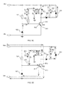
Fig.3A is a schematic diagram for a starting phase of the driving system for the semiconductor light source according to the embodiment of the present disclosure. -
Fig.3B is a schematic diagram for a first energy storing phase of the driving system for the semiconductor light source according to the embodiment of the present disclosure. -
Fig.3C is a schematic diagram for an energy releasing phase of the driving system for the semiconductor light source according to the embodiment of the present disclosure. -
Fig.3D is a schematic diagram for a second energy storing phase of the driving system for the semiconductor light source according to the embodiment of the present disclosure. -
Fig.4 shows a waveform of voltages and currents when the driving system for the semiconductor light source according to the embodiment of the present disclosure operates. - In the above described accompanying drawings, same reference numerals indicate same, similar or corresponding elements or functions.
- Below, particular embodiments of the present disclosure will be described in detail with reference to the accompanying drawings.
-
Fig.1 is a schematic diagram of a driving system for a semiconductor light source according to an embodiment of the present disclosure. - In
Fig.1 , Vin represents an input voltage. The input voltage is a Direct Current (DC) input voltage, and may be a rectified DC voltage, or a rectified and filtered DC voltage. I represents a starting means, II represents a transformer, III represents a switching means, IV represents an outputting means, V represents a semiconductor light source as a load. - The starting means I is used for ensuring the switching means to be in a turn-on state during a starting phase (that is, when the input signal Vin is initially supplied). The transformer II includes a first coil and a second coil coupled to each other, the second coil is used for receiving the input voltage and for storing or releasing energy under the control of the switching means III. An induced signal is generated on the first coil of the transformer due to a coupling effect between the first coil and the second coil and is used for controlling turn-on or turn-off of the switching means III. The outputting means is used for supplying power to the semiconductor light source differently according to the energy saving or releasing of the second coil.
-
Fig.2 is a circuit diagram of a driving system for a semiconductor light source according to an embodiment of the present disclosure. - In
Fig.2 , the starting means I includes afirst resistor 101 and afirst diode 102 connected together in series. A first terminal of thefirst resistor 101 is connected to a first voltage input terminal, and a second terminal of thefirst resistor 101 is connected to a first terminal of thefirst diode 102, and a second terminal of thefirst diode 102 is connected to a second voltage input terminal. The second voltage input terminal can be grounded directly. Those skilled in the art should understand that the resistor may be replaced by other resistive elements, and the diode may also be replaced by other unidirectional conducting elements (for example, a triode). - The transformer II includes a
first coil 201 and asecond coil 202 coupled to each other. Thefirst coil 201, afirst capacitor 203 and asecond resistor 204 are connected in series. A first terminal of thefirst coil 201 is connected to a first terminal of thefirst capacitor 203, and a second terminal of thefirst capacitor 203 is connected to a first terminal of thesecond resistor 204. A second terminal of thefirst coil 201 is grounded. A first terminal of thesecond coil 202 is connected to the first voltage input terminal. The first terminal of thefirst coil 201 and the first terminal ofsecond coil 202 are dotted terminals. Thesecond coil 202 and the switching means are connected in series, so as to store or release energy under the control of the switching means. Those skilled in the art should understand that the capacitor may be replaced by other elements with a capacitive function, and the resistors may also be replaced by other elements with a resistive function. - The switching means III in
Fig.2 includes atriode 300 including abase 301, acollector 302 and anemitter 303. In the embodiment of the present disclosure, theemitter 303 is connected to the second voltage input terminal. - The switching means III may be a MOS transistor, a gate of the MOS transistor is equivalent to the base of the triode, a source of the MOS transistor is equivalent to the collector of the triode, and a drain of the MOS transistor is equivalent to the emitter of the triode.
- A second terminal of the
second resistor 204 is connected to thebase 301 of thetriode 300, and is connected to the second terminal of thefirst resistor 101. The second terminal of thesecond coil 202 is connected to thecollector 302 of thetriode 300. - The outputting means IV includes a
second diode 401 and asecond capacitor 402 connected together in series, a series connection of thesecond diode 401 and thesecond capacitor 402 is connected to thesecond coil 202 in parallel. A first terminal of thesecond diode 401 is connected to the second terminal of thesecond coil 202, the second terminal of thesecond diode 401 is connected to a second terminal of thesecond capacitor 402, and a first terminal of thesecond capacitor 402 is connected to the first voltage input terminal. In addition, the first terminal of thesecond capacitor 402 is connected to a first terminal of a semiconductor light source as a load V, and the second terminal of thesecond capacitor 402 is connected to a second terminal of the semiconductor light source as the load V. - The semiconductor light source as the load V includes one or more semiconductor light sources, for example, lighting sources such as LEDs or OLEDs, connected in various manners.
- With reference to
Fig.3A-3D , an operational principle of the driving system for the semiconductor light source described in the embodiment of the present disclosure will be described as follows. - During a starting phase, as shown in
Fig.3A , after the driving system for the semiconductor light source described in the embodiment of the present disclosure is connected to the DC input voltage Vin, a current 11 is generated by Vin being discharged through thefirst resistor 101 and thebase 301 and theemitter 303 of thetriode 300, such that an electric conduction is established between thecollector 302 and theemitter 303 of thetriode 300. A current 12 is generated by Vin being discharged through thesecond coil 202 and thecollector 302 and theemitter 303 of thetriode 300. Thereafter, the driving system of the semiconductor light source described in the embodiment of the present disclosure enters into a first energy storing phase. - During the first energy storing phase, as shown in
Fig.3B , 12 flows through thesecond coil 202, thesecond coil 202 stores energy, and a voltage V2 is generated across thesecond coil 202, meanwhile an induced electromotive force (EMF) V1 is generated on thefirst coil 201 due to a coupling effect between thefirst coil 201 and thesecond coil 202, and a current 13 is generated by V1 being discharged through thefirst capacitor 203, thesecond resistor 204 and thebase 301 and theemitter 303 of thetriode 300. Thefirst capacitor 203 is charged by I3. A voltage V3 with a direction as shown is generated across thefirst capacitor 203. With increase of V3, I3 is reduced, and in turn thetriode 300 is turned off. However, since the current flowing through thesecond coil 202 cannot change suddenly, the current flows to the semiconductor light source as the load through thesecond diode 401 and enables the voltage V2 across thesecond coil 202 to be inverted. Thereafter, the driving system for the semiconductor light source as described in the embodiment of the present disclosure enters into an energy releasing phase, and the semiconductor light source as the load V starts to emit light. - During an energy releasing phase, as shown
Fig.3C , likewise, the induced EMF V1 on thefirst coil 201 due to the coupling effect between thefirst coil 201 and thesecond coil 202 are inverted. A current 14 is generated by V1 being discharged through thefirst diode 102, thesecond resistor 204 and thefirst capacitor 203. Thetriode 300 is turned off. V2 across thesecond coil 202 is discharged through thesecond diode 401 and the semiconductor light source as the load V, thesecond coil 202 releases energy, and meanwhile thesecond capacitor 402 is charged to generate a voltage V5 across thesecond capacitor 402. The voltage V4 is inverted since thefirst capacitor 203 is charged reversely by the current 14. Thesecond coil 202 stops releasing energy when the voltage V2 across thesecond coil 202 is decreased to be lower than the voltage V5 across thesecond capacitor 402. Thereafter, the driving system for the semiconductor light source described in the embodiment of the present disclosure enters into a second energy storing phase different from the first energy storing phase. In the second energy storing phase, the semiconductor light source as the load V emits light. - During the second energy storing phase, as shown in
Fig.3D , the voltage V5 across thesecond capacitor 402 is discharged through the semiconductor light source as the load, and the voltage V4 across thefirst capacitor 203 is discharged through theresistor 204, thebase 301 and theemitter 303 of thetriode 300 and thefirst coil 201, such that an electric conduction is established between thecollector 302 and theemitter 303 of thetriode 300. A current 12 is generated by Vin being discharged through thesecond coil 202 and thecollector 302 and theemitter 303 of thetriode 300. Thesecond coil 202 stores energy and generates a voltage V2 across thesecond coil 202. Thereafter, descriptions will be given continuously with reference to the transformer II and the switching means III inFig.3B . An induced EMF V1 is generated on thefirst coil 201 due to the coupling effect between thefirst coil 201 andsecond coil 202, and a current 13 is generated by V1 being discharged through thefirst capacitor 203, thesecond resistor 204 and thebase 301 and theemitter 303 of thetriode 300. Thefirst capacitor 203 is charged by I3. A voltage V3 with a direction as shown is generated across thefirst capacitor 203. With increase of V3, I3 is reduced, and in turn thetriode 300 is turned-off. However, since the current flowing through thesecond coil 202 cannot change suddenly, the current flows to the semiconductor light source as the load through thesecond diode 401 and enables the voltage V2 across thesecond coil 202 to be inverted. Thereafter, the driving system for the semiconductor light source as described in the embodiment of the present disclosure enters into the energy releasing phase again. - Thereafter, the driving system for the semiconductor light source as described in the embodiment of the present disclosure re-enters into the second energy storing phase from the energy releasing phase, and a repeated loop is thus formed.
- Below, operations of the
triode 300 during the respective phases will be described in further detail. - During the starting phase, as shown in
Fig.3A , the current I1 is generated by Vin through thefirst resistor 101 and thebase 301 and theemitter 303 of thetriode 300, such that thetriode 300 is turned on and operates in an amplification region. - Then, during the first energy storing phase, as shown in
Fig.3B , the current 13 is generated by the induced EMF V1 on thefirst coil 201 through thefirst capacitor 203, thesecond resistor 204 and thebase 301 and theemitter 303 of thetriode 300, such that thetriode 300 enters into a saturation region. While the current 13 charges thefirst capacitor 203 to enable the voltage V3 across thefirst capacitor 203 to be increased, the current 13 is decreased to enable thetriode 300 to quit the saturation region and enter into a cutoff region. However, since the current 12 flowing through thesecond coil 202 cannot change suddenly, the current 12 flows to the semiconductor light source as the load through thesecond diode 401 and enables the voltage V2 across thesecond coil 202 to be inverted. - Thereafter, during the energy releasing phase, as shown
Fig.3C , thetriode 300 is turned off, the voltage across thefirst coil 201 is inverted while the voltage across thesecond coil 202 is inverted, and thefirst capacitor 203 is charged reversely through thesecond resistor 204 and thefirst diode 102. - Then, during the second energy storing phase, as shown in
Fig.3D , the current 13 is generated by the induced EMF Vin on thefirst coil 201 through thefirst capacitor 203, thesecond resistor 204 and thebase 301 and theemitter 303 of thetriode 300, such that thetriode 300 enters the saturation region again and thesecond coil 202 begins to store energy. Then, while the current 13 charges thefirst capacitor 203 to enable the voltage V3 across thefirst capacitor 203 to be increased, the current 13 is decreased to enable thetriode 300 to quit the saturation region and enter into the cutoff region. - Thereafter, the energy releasing phase is re-entered. In such manner, a repeated loop is thus formed from the second energy storing phase and the energy releasing phase.
- As shown in
Fig.4 , a waveform of voltages and currents when the driving system for the semiconductor light source according to the embodiment of the present disclosure operates is given. It should be noted that the waveform for the starting phase is not shown inFig.4 . - At a timing t0, the current 12 is generated by Vin being discharged through the
second coil 202 and thecollector 302 and theemitter 303 of thetriode 300, and thesecond coil 202 begins to store energy; the induced EMF V1 is generated on thefirst coil 201, the current 13 is generated by V1 being discharged through thefirst capacitor 203, thesecond resistor 204 and thebase 301 and theemitter 303 of thetriode 300, and thefirst capacitor 203 is charged by I3. - At a timing t1, the voltage V3 across the
first capacitor 203 is approximately equal to the induced EMF V1 generated on thefirst coil 201, I3 is decreased such that thetriode 300 is turned off. However, since the current 12 flowing through thesecond coil 202 cannot change suddenly, thesecond coil 202 generates a current Io which flows through thesecond diode 401 to enable the semiconductor light source as the load V to emit light, the current Io is gradually decreased, the voltage V2 across thesecond coil 202 is inverted and begins to release energy. - Then, at a timing t2, the voltage across the
second capacitor 402 is equal to the voltage V2 across thesecond coil 202, and thesecond coil 202 stops releasing energy and thesecond capacitor 402 supplies power to the semiconductor light source as the load V. On the other hand, the voltage V4 across thefirst capacitor 203 is discharged through theresistor 204, thebase 301 and theemitter 303 of thetriode 300 and thefirst coil 201 to generate the current 15, such that the electrical conduction between thecollector 302 and theemitter 303 of thetriode 300 is established; the current 12 is generated by Vin being discharged through thesecond coil 202 and thecollector 302 and theemitter 303 of thetriode 300, and thesecond coil 202 begins to store energy. - Thereafter, at a timing t3, the voltage V3 across the
first capacitor 203 is approximately equal to the induced EMF V1 generated on thefirst coil 201, I3 is decreased such that thetriode 300 is turned off. However, since the current 12 flowing through thesecond coil 202 cannot change suddenly, thesecond coil 202 generates a current Io which flows through thesecond diode 401 to enable the semiconductor light source as the load V to emit light, the current Io is gradually decreased, the voltage V2 across thesecond coil 202 is inverted and thesecond coil 202 begins to release energy. - Then, from a timing t4, the operation sequence from t2 to t4 is repeated. That is, the operation sequence from t2 to t4 is repeated during a time period t4-t6, a time period t6-68, and so on.
- Although a NPN type triode is adopted to constitute the switching means III in the embodiments of the present disclosure, the present disclosure is not limited thereto. Those skilled in the art should easily think of adopting a PNP type triode to constitute the switching means III and modify the connection configuration of the starting means I, the transformer II, the switching means III and the outputting means IV correspondingly, such modification should be included in the scope of the present disclosure.
- In addition, those skilled in the art should also easily think of adopting a N type transistor or a P type transistor to constitute the switching means and modify the connection configuration of the starting means I, the transformer II, the switching means III and the outputting means IV correspondingly, such modification should also be included in the scope of the present disclosure.
- The above embodiments are only illustrative and should not make any limitation to technical solutions of the present disclosure. Although the present disclosure has been described with reference to preferred embodiments thereof, those skilled in the art should understand that the technical solution of the present disclosure may be modified or equivalently replaced without departing the spirit and scope of the technical solutions of the present disclosure. Such modifications and equivalent replacement are intended to be included within the spirit and scope of the present disclosure.
Claims (10)
- A driving system for a semiconductor light source including:a transformer including a first coil and a second coil coupled to each other, the second coil receiving an input voltage;a switching means connected to the second coil of the transformer in series and for controlling energy-storing and energy-releasing of the second coil;an outputting means connected to the second coil of the transformer in parallel and for supplying power to the semiconductor light source,wherein an induced signal is generated on the first coil of the transformer due to a coupling effect between the first coil and the second coil and is used for controlling turn-on or turn-off of the switching means.
- The driving system of claim 1, wherein the second coil supplies power to the semiconductor light source and charges the outputting means when the second coil is in energy-releasing, and the outputting means supplies power to the semiconductor light source when the second coil is in energy-storing.
- The driving system of claim 1, further including a starting means for starting the switching means when the input signal is initially supplied.
- The driving system of claim 1, wherein the switching means includes a switch and at least one discrete element, wherein the at least one discrete element is connected between the first coil and a control terminal of the switch, and the induced signal is used to control the switch via the at least one discrete element.
- The driving system of claim 4, wherein the at least one discrete element includes a capacitive element.
- The driving system of claim 5, wherein the at least one discrete element further includes a resistive element, and the capacitive element and the resistive element are connected in series.
- The driving system of claim 3, wherein the starting means includes a resistive element and a unidirectional conducting element connected together in series, a connection point between the resistive element and the unidirectional conducting element is connected to the control terminal of the switch.
- A semiconductor lighting device including:a semiconductor light source as a load;a transformer including a first coil and a second coil coupled to each other, the second coil receiving an input voltage;a switching means connected to the second coil of the transformer in series and for controlling energy-storing and energy-releasing of the second coil;an outputting means connected to the second coil of the transformer in parallel and for supplying power to the semiconductor light source as the load,wherein an induced signal is generated on the first coil of the transformer due to a coupling effect between the first coil and the second coil and is used for controlling turn-on or turn-off of the switching means.
- The semiconductor lighting device of claim 8, wherein the switching means includes a switch and at least one discrete element, wherein the at least one discrete element is connected between the first coil and a control terminal of the switch, and the induced signal is used to control the switch via the at least one discrete element.
- The semiconductor lighting device of claim 8, further including a starting means for starting the switching means when the input signal is initially supplied.
Applications Claiming Priority (2)
| Application Number | Priority Date | Filing Date | Title |
|---|---|---|---|
| CN201210181467.1A CN103458559B (en) | 2012-06-04 | 2012-06-04 | Drive system of semiconductor light source and semiconductor illumination device |
| PCT/CN2013/076105 WO2013181993A1 (en) | 2012-06-04 | 2013-05-22 | Drive system of semiconductor light source, and semiconductor lighting device |
Publications (3)
| Publication Number | Publication Date |
|---|---|
| EP2785149A1 true EP2785149A1 (en) | 2014-10-01 |
| EP2785149A4 EP2785149A4 (en) | 2015-08-19 |
| EP2785149B1 EP2785149B1 (en) | 2017-04-19 |
Family
ID=49711352
Family Applications (1)
| Application Number | Title | Priority Date | Filing Date |
|---|---|---|---|
| EP13800096.3A Active EP2785149B1 (en) | 2012-06-04 | 2013-05-22 | Drive system of semiconductor light source, and semiconductor lighting device |
Country Status (10)
| Country | Link |
|---|---|
| US (1) | US9967930B2 (en) |
| EP (1) | EP2785149B1 (en) |
| JP (1) | JP5757644B1 (en) |
| CN (1) | CN103458559B (en) |
| BR (1) | BR112014030295B1 (en) |
| DE (1) | DE202013012382U1 (en) |
| IN (1) | IN2015DN00014A (en) |
| TW (1) | TW201352060A (en) |
| WO (1) | WO2013181993A1 (en) |
| ZA (1) | ZA201409526B (en) |
Family Cites Families (20)
| Publication number | Priority date | Publication date | Assignee | Title |
|---|---|---|---|---|
| JP3416863B2 (en) | 1994-06-27 | 2003-06-16 | 松下電工株式会社 | Power supply |
| TW291620B (en) * | 1995-05-10 | 1996-11-21 | Philips Electronics Nv | |
| CN1498052A (en) * | 2002-10-03 | 2004-05-19 | 模拟微电子学股份有限公司 | Method and system for driving CCFL |
| EP1501179B1 (en) * | 2003-07-15 | 2008-09-17 | Friwo Mobile Power GmbH | Freely oscillating flyback converter with current and voltage limitation |
| US6856103B1 (en) * | 2003-09-17 | 2005-02-15 | Varon Lighting, Inc. | Voltage regulator for line powered linear and switching power supply |
| JP5025913B2 (en) * | 2005-05-13 | 2012-09-12 | シャープ株式会社 | LED drive circuit, LED illumination device, and backlight |
| CN101048052A (en) * | 2006-03-30 | 2007-10-03 | 徐富雄 | Fan-type display for cooling |
| RU2479955C2 (en) * | 2007-05-07 | 2013-04-20 | Конинклейке Филипс Электроникс Н.В. | Device and method of lighting based on led with high capacity ratio |
| US8498134B2 (en) * | 2008-05-15 | 2013-07-30 | Fraunhofer-Gesellschaft Zur Foerderung Der Angewandten Forschung E.V. | Voltage converter circuit and method for a clock supply of energy to an energy storage |
| JP4586905B2 (en) * | 2008-08-13 | 2010-11-24 | ソニー株式会社 | Light emitting diode drive device |
| US7952301B2 (en) * | 2008-12-12 | 2011-05-31 | Biegel George E | Auto-dimming apparatus for controlling power delivered to a load |
| US8305004B2 (en) * | 2009-06-09 | 2012-11-06 | Stmicroelectronics, Inc. | Apparatus and method for constant power offline LED driver |
| US8143800B2 (en) * | 2009-06-22 | 2012-03-27 | O2Micro, Inc. | Circuits and methods for driving a load with power factor correction function |
| TWI538553B (en) * | 2009-08-25 | 2016-06-11 | 皇家飛利浦電子股份有限公司 | Multichannel lighting unit and driver for supplying current to light sources in multichannel lighting unit |
| CN102042508A (en) * | 2009-10-23 | 2011-05-04 | 陈进祥 | Light source device |
| JP5457927B2 (en) * | 2010-04-23 | 2014-04-02 | セミコンダクター・コンポーネンツ・インダストリーズ・リミテッド・ライアビリティ・カンパニー | Light emitting element control circuit |
| WO2012011288A1 (en) * | 2010-07-22 | 2012-01-26 | パナソニック株式会社 | Lighting circuit, lamp and illumination device |
| JP5408161B2 (en) * | 2011-03-11 | 2014-02-05 | Smk株式会社 | Self-excited switching power supply circuit |
| TWM423415U (en) * | 2011-10-05 | 2012-02-21 | Darfon Electronics Corp | Non-isolated buck-boost light emitting diode driving circuit |
| CN202663608U (en) * | 2012-06-04 | 2013-01-09 | 欧普照明股份有限公司 | Driving system for semiconductor light source and semiconductor illuminating device |
-
2012
- 2012-06-04 CN CN201210181467.1A patent/CN103458559B/en active Active
-
2013
- 2013-05-22 WO PCT/CN2013/076105 patent/WO2013181993A1/en not_active Ceased
- 2013-05-22 US US14/404,775 patent/US9967930B2/en active Active
- 2013-05-22 DE DE202013012382.6U patent/DE202013012382U1/en not_active Expired - Lifetime
- 2013-05-22 JP JP2015515375A patent/JP5757644B1/en not_active Expired - Fee Related
- 2013-05-22 BR BR112014030295-2A patent/BR112014030295B1/en not_active IP Right Cessation
- 2013-05-22 EP EP13800096.3A patent/EP2785149B1/en active Active
- 2013-06-04 TW TW102119710A patent/TW201352060A/en unknown
-
2014
- 2014-12-23 ZA ZA2014/09526A patent/ZA201409526B/en unknown
-
2015
- 2015-01-01 IN IN14DEN2015 patent/IN2015DN00014A/en unknown
Also Published As
| Publication number | Publication date |
|---|---|
| US20150145432A1 (en) | 2015-05-28 |
| BR112014030295B1 (en) | 2021-08-17 |
| ZA201409526B (en) | 2016-08-31 |
| HK1192097A1 (en) | 2014-08-08 |
| IN2015DN00014A (en) | 2015-05-22 |
| JP5757644B1 (en) | 2015-07-29 |
| CN103458559B (en) | 2015-04-15 |
| TW201352060A (en) | 2013-12-16 |
| CN103458559A (en) | 2013-12-18 |
| HK1199593A1 (en) | 2015-07-03 |
| JP2015523684A (en) | 2015-08-13 |
| WO2013181993A1 (en) | 2013-12-12 |
| TWI508614B (en) | 2015-11-11 |
| US9967930B2 (en) | 2018-05-08 |
| EP2785149B1 (en) | 2017-04-19 |
| DE202013012382U1 (en) | 2016-08-03 |
| BR112014030295A2 (en) | 2017-06-27 |
| EP2785149A4 (en) | 2015-08-19 |
Similar Documents
| Publication | Publication Date | Title |
|---|---|---|
| CN101282083A (en) | BUCK drive circuit | |
| CN201656779U (en) | Low power consumption standby circuit and electrical appliances | |
| CN112913329A (en) | Driver circuit and associated lamp | |
| JP6737458B2 (en) | Protection circuit and LED drive circuit | |
| CN102820784B (en) | BJT (bipolar junction transistor)-type auto-excitation Buck converter with small main switching tube driving loss | |
| US9967930B2 (en) | Drive system of semiconductor light source, and semiconductor lighting device | |
| US9881589B2 (en) | Backlight source driving circuit and display apparatus | |
| CN102684493B (en) | BJT type self-excited Boost converter equipped with main switching tube with low drive loss | |
| CN202663608U (en) | Driving system for semiconductor light source and semiconductor illuminating device | |
| CN105515357B (en) | A kind of DCDC current-limiting circuits | |
| CN211429598U (en) | Drive circuit and electronic product | |
| CN102684487B (en) | BJT type self-excited Sepic converter equipped with main switching tube with low drive loss | |
| CN202617002U (en) | Feedback BJT type self-excited Boost converter | |
| CN102710132B (en) | Feedback type bipolar junction transistor (BJT) self-exciting Boost converter | |
| HK1199593B (en) | Drive system of semiconductor light source, and semiconductor lighting device | |
| CN107087328B (en) | LED driving circuit | |
| CN102723866B (en) | BJT-typed self-exciting Cuk converter provided with main switching transistor having small driving loss | |
| WO2015101506A1 (en) | Lighting arrangement | |
| CN105873310A (en) | LED power source starting circuit | |
| CN203206547U (en) | Timing boost bidirectional controller for battery lamp | |
| WO2012144274A1 (en) | Led lighting device and led illuminating device | |
| KR101401901B1 (en) | The power supply for driving LED modules and the lighting apparatus including the same | |
| JP2013118267A (en) | Led lighting device and control method of led lighting device | |
| CN203072211U (en) | LED driving system and semi-conductor lighting device | |
| HK1192097B (en) | Driving system for semiconductor light source and semiconductor lighting device |
Legal Events
| Date | Code | Title | Description |
|---|---|---|---|
| REG | Reference to a national code |
Ref country code: DE Ref legal event code: R138 Ref document number: 202013012382 Country of ref document: DE Free format text: GERMAN DOCUMENT NUMBER IS 602013020100 |
|
| PUAI | Public reference made under article 153(3) epc to a published international application that has entered the european phase |
Free format text: ORIGINAL CODE: 0009012 |
|
| 17P | Request for examination filed |
Effective date: 20140624 |
|
| AK | Designated contracting states |
Kind code of ref document: A1 Designated state(s): AL AT BE BG CH CY CZ DE DK EE ES FI FR GB GR HR HU IE IS IT LI LT LU LV MC MK MT NL NO PL PT RO RS SE SI SK SM TR |
|
| REG | Reference to a national code |
Ref country code: HK Ref legal event code: DE Ref document number: 1199593 Country of ref document: HK |
|
| RA4 | Supplementary search report drawn up and despatched (corrected) |
Effective date: 20150716 |
|
| RIC1 | Information provided on ipc code assigned before grant |
Ipc: H05B 37/02 20060101AFI20150710BHEP Ipc: H05B 33/08 20060101ALI20150710BHEP Ipc: F21S 2/00 20060101ALI20150710BHEP |
|
| DAX | Request for extension of the european patent (deleted) | ||
| 17Q | First examination report despatched |
Effective date: 20160502 |
|
| GRAP | Despatch of communication of intention to grant a patent |
Free format text: ORIGINAL CODE: EPIDOSNIGR1 |
|
| STAA | Information on the status of an ep patent application or granted ep patent |
Free format text: STATUS: GRANT OF PATENT IS INTENDED |
|
| INTG | Intention to grant announced |
Effective date: 20161107 |
|
| GRAS | Grant fee paid |
Free format text: ORIGINAL CODE: EPIDOSNIGR3 |
|
| GRAA | (expected) grant |
Free format text: ORIGINAL CODE: 0009210 |
|
| STAA | Information on the status of an ep patent application or granted ep patent |
Free format text: STATUS: THE PATENT HAS BEEN GRANTED |
|
| AK | Designated contracting states |
Kind code of ref document: B1 Designated state(s): AL AT BE BG CH CY CZ DE DK EE ES FI FR GB GR HR HU IE IS IT LI LT LU LV MC MK MT NL NO PL PT RO RS SE SI SK SM TR |
|
| REG | Reference to a national code |
Ref country code: GB Ref legal event code: FG4D |
|
| REG | Reference to a national code |
Ref country code: CH Ref legal event code: EP |
|
| REG | Reference to a national code |
Ref country code: AT Ref legal event code: REF Ref document number: 887050 Country of ref document: AT Kind code of ref document: T Effective date: 20170515 |
|
| REG | Reference to a national code |
Ref country code: IE Ref legal event code: FG4D |
|
| REG | Reference to a national code |
Ref country code: FR Ref legal event code: PLFP Year of fee payment: 5 |
|
| REG | Reference to a national code |
Ref country code: DE Ref legal event code: R096 Ref document number: 602013020100 Country of ref document: DE |
|
| REG | Reference to a national code |
Ref country code: SE Ref legal event code: TRGR |
|
| REG | Reference to a national code |
Ref country code: NL Ref legal event code: FP |
|
| REG | Reference to a national code |
Ref country code: NO Ref legal event code: T2 Effective date: 20170419 |
|
| REG | Reference to a national code |
Ref country code: LT Ref legal event code: MG4D |
|
| PG25 | Lapsed in a contracting state [announced via postgrant information from national office to epo] |
Ref country code: LT Free format text: LAPSE BECAUSE OF FAILURE TO SUBMIT A TRANSLATION OF THE DESCRIPTION OR TO PAY THE FEE WITHIN THE PRESCRIBED TIME-LIMIT Effective date: 20170419 Ref country code: GR Free format text: LAPSE BECAUSE OF FAILURE TO SUBMIT A TRANSLATION OF THE DESCRIPTION OR TO PAY THE FEE WITHIN THE PRESCRIBED TIME-LIMIT Effective date: 20170720 Ref country code: ES Free format text: LAPSE BECAUSE OF FAILURE TO SUBMIT A TRANSLATION OF THE DESCRIPTION OR TO PAY THE FEE WITHIN THE PRESCRIBED TIME-LIMIT Effective date: 20170419 Ref country code: HR Free format text: LAPSE BECAUSE OF FAILURE TO SUBMIT A TRANSLATION OF THE DESCRIPTION OR TO PAY THE FEE WITHIN THE PRESCRIBED TIME-LIMIT Effective date: 20170419 |
|
| PG25 | Lapsed in a contracting state [announced via postgrant information from national office to epo] |
Ref country code: BG Free format text: LAPSE BECAUSE OF FAILURE TO SUBMIT A TRANSLATION OF THE DESCRIPTION OR TO PAY THE FEE WITHIN THE PRESCRIBED TIME-LIMIT Effective date: 20170719 Ref country code: IS Free format text: LAPSE BECAUSE OF FAILURE TO SUBMIT A TRANSLATION OF THE DESCRIPTION OR TO PAY THE FEE WITHIN THE PRESCRIBED TIME-LIMIT Effective date: 20170819 Ref country code: PL Free format text: LAPSE BECAUSE OF FAILURE TO SUBMIT A TRANSLATION OF THE DESCRIPTION OR TO PAY THE FEE WITHIN THE PRESCRIBED TIME-LIMIT Effective date: 20170419 Ref country code: RS Free format text: LAPSE BECAUSE OF FAILURE TO SUBMIT A TRANSLATION OF THE DESCRIPTION OR TO PAY THE FEE WITHIN THE PRESCRIBED TIME-LIMIT Effective date: 20170419 Ref country code: LV Free format text: LAPSE BECAUSE OF FAILURE TO SUBMIT A TRANSLATION OF THE DESCRIPTION OR TO PAY THE FEE WITHIN THE PRESCRIBED TIME-LIMIT Effective date: 20170419 |
|
| REG | Reference to a national code |
Ref country code: CH Ref legal event code: PL |
|
| REG | Reference to a national code |
Ref country code: DE Ref legal event code: R097 Ref document number: 602013020100 Country of ref document: DE |
|
| PG25 | Lapsed in a contracting state [announced via postgrant information from national office to epo] |
Ref country code: CZ Free format text: LAPSE BECAUSE OF FAILURE TO SUBMIT A TRANSLATION OF THE DESCRIPTION OR TO PAY THE FEE WITHIN THE PRESCRIBED TIME-LIMIT Effective date: 20170419 Ref country code: DK Free format text: LAPSE BECAUSE OF FAILURE TO SUBMIT A TRANSLATION OF THE DESCRIPTION OR TO PAY THE FEE WITHIN THE PRESCRIBED TIME-LIMIT Effective date: 20170419 Ref country code: EE Free format text: LAPSE BECAUSE OF FAILURE TO SUBMIT A TRANSLATION OF THE DESCRIPTION OR TO PAY THE FEE WITHIN THE PRESCRIBED TIME-LIMIT Effective date: 20170419 Ref country code: MC Free format text: LAPSE BECAUSE OF FAILURE TO SUBMIT A TRANSLATION OF THE DESCRIPTION OR TO PAY THE FEE WITHIN THE PRESCRIBED TIME-LIMIT Effective date: 20170419 Ref country code: SK Free format text: LAPSE BECAUSE OF FAILURE TO SUBMIT A TRANSLATION OF THE DESCRIPTION OR TO PAY THE FEE WITHIN THE PRESCRIBED TIME-LIMIT Effective date: 20170419 Ref country code: RO Free format text: LAPSE BECAUSE OF FAILURE TO SUBMIT A TRANSLATION OF THE DESCRIPTION OR TO PAY THE FEE WITHIN THE PRESCRIBED TIME-LIMIT Effective date: 20170419 |
|
| REG | Reference to a national code |
Ref country code: IE Ref legal event code: MM4A |
|
| PLBE | No opposition filed within time limit |
Free format text: ORIGINAL CODE: 0009261 |
|
| STAA | Information on the status of an ep patent application or granted ep patent |
Free format text: STATUS: NO OPPOSITION FILED WITHIN TIME LIMIT |
|
| PG25 | Lapsed in a contracting state [announced via postgrant information from national office to epo] |
Ref country code: IT Free format text: LAPSE BECAUSE OF FAILURE TO SUBMIT A TRANSLATION OF THE DESCRIPTION OR TO PAY THE FEE WITHIN THE PRESCRIBED TIME-LIMIT Effective date: 20170419 Ref country code: LI Free format text: LAPSE BECAUSE OF NON-PAYMENT OF DUE FEES Effective date: 20170531 Ref country code: CH Free format text: LAPSE BECAUSE OF NON-PAYMENT OF DUE FEES Effective date: 20170531 Ref country code: SM Free format text: LAPSE BECAUSE OF FAILURE TO SUBMIT A TRANSLATION OF THE DESCRIPTION OR TO PAY THE FEE WITHIN THE PRESCRIBED TIME-LIMIT Effective date: 20170419 |
|
| 26N | No opposition filed |
Effective date: 20180122 |
|
| PG25 | Lapsed in a contracting state [announced via postgrant information from national office to epo] |
Ref country code: LU Free format text: LAPSE BECAUSE OF NON-PAYMENT OF DUE FEES Effective date: 20170522 |
|
| REG | Reference to a national code |
Ref country code: HK Ref legal event code: GR Ref document number: 1199593 Country of ref document: HK |
|
| PG25 | Lapsed in a contracting state [announced via postgrant information from national office to epo] |
Ref country code: IE Free format text: LAPSE BECAUSE OF NON-PAYMENT OF DUE FEES Effective date: 20170522 |
|
| REG | Reference to a national code |
Ref country code: FR Ref legal event code: PLFP Year of fee payment: 6 |
|
| PG25 | Lapsed in a contracting state [announced via postgrant information from national office to epo] |
Ref country code: SI Free format text: LAPSE BECAUSE OF FAILURE TO SUBMIT A TRANSLATION OF THE DESCRIPTION OR TO PAY THE FEE WITHIN THE PRESCRIBED TIME-LIMIT Effective date: 20170419 |
|
| PG25 | Lapsed in a contracting state [announced via postgrant information from national office to epo] |
Ref country code: MT Free format text: LAPSE BECAUSE OF NON-PAYMENT OF DUE FEES Effective date: 20170522 |
|
| PG25 | Lapsed in a contracting state [announced via postgrant information from national office to epo] |
Ref country code: HU Free format text: LAPSE BECAUSE OF FAILURE TO SUBMIT A TRANSLATION OF THE DESCRIPTION OR TO PAY THE FEE WITHIN THE PRESCRIBED TIME-LIMIT; INVALID AB INITIO Effective date: 20130522 |
|
| PG25 | Lapsed in a contracting state [announced via postgrant information from national office to epo] |
Ref country code: CY Free format text: LAPSE BECAUSE OF FAILURE TO SUBMIT A TRANSLATION OF THE DESCRIPTION OR TO PAY THE FEE WITHIN THE PRESCRIBED TIME-LIMIT Effective date: 20170419 |
|
| PG25 | Lapsed in a contracting state [announced via postgrant information from national office to epo] |
Ref country code: MK Free format text: LAPSE BECAUSE OF FAILURE TO SUBMIT A TRANSLATION OF THE DESCRIPTION OR TO PAY THE FEE WITHIN THE PRESCRIBED TIME-LIMIT Effective date: 20170419 |
|
| REG | Reference to a national code |
Ref country code: AT Ref legal event code: UEP Ref document number: 887050 Country of ref document: AT Kind code of ref document: T Effective date: 20170419 |
|
| PG25 | Lapsed in a contracting state [announced via postgrant information from national office to epo] |
Ref country code: TR Free format text: LAPSE BECAUSE OF FAILURE TO SUBMIT A TRANSLATION OF THE DESCRIPTION OR TO PAY THE FEE WITHIN THE PRESCRIBED TIME-LIMIT Effective date: 20170419 |
|
| PG25 | Lapsed in a contracting state [announced via postgrant information from national office to epo] |
Ref country code: PT Free format text: LAPSE BECAUSE OF FAILURE TO SUBMIT A TRANSLATION OF THE DESCRIPTION OR TO PAY THE FEE WITHIN THE PRESCRIBED TIME-LIMIT Effective date: 20170419 |
|
| PG25 | Lapsed in a contracting state [announced via postgrant information from national office to epo] |
Ref country code: AL Free format text: LAPSE BECAUSE OF FAILURE TO SUBMIT A TRANSLATION OF THE DESCRIPTION OR TO PAY THE FEE WITHIN THE PRESCRIBED TIME-LIMIT Effective date: 20170419 |
|
| PGFP | Annual fee paid to national office [announced via postgrant information from national office to epo] |
Ref country code: AT Payment date: 20240422 Year of fee payment: 12 |
|
| PGFP | Annual fee paid to national office [announced via postgrant information from national office to epo] |
Ref country code: NO Payment date: 20240426 Year of fee payment: 12 Ref country code: FR Payment date: 20240524 Year of fee payment: 12 Ref country code: FI Payment date: 20240422 Year of fee payment: 12 |
|
| PGFP | Annual fee paid to national office [announced via postgrant information from national office to epo] |
Ref country code: SE Payment date: 20240516 Year of fee payment: 12 Ref country code: BE Payment date: 20240515 Year of fee payment: 12 |
|
| PGFP | Annual fee paid to national office [announced via postgrant information from national office to epo] |
Ref country code: NL Payment date: 20250429 Year of fee payment: 13 |
|
| PGFP | Annual fee paid to national office [announced via postgrant information from national office to epo] |
Ref country code: DE Payment date: 20250513 Year of fee payment: 13 |
|
| PGFP | Annual fee paid to national office [announced via postgrant information from national office to epo] |
Ref country code: GB Payment date: 20250521 Year of fee payment: 13 |
|
| PG25 | Lapsed in a contracting state [announced via postgrant information from national office to epo] |
Ref country code: NO Free format text: LAPSE BECAUSE OF NON-PAYMENT OF DUE FEES Effective date: 20250531 |
|
| PG25 | Lapsed in a contracting state [announced via postgrant information from national office to epo] |
Ref country code: AT Free format text: LAPSE BECAUSE OF NON-PAYMENT OF DUE FEES Effective date: 20250522 |
|
| PG25 | Lapsed in a contracting state [announced via postgrant information from national office to epo] |
Ref country code: FI Free format text: LAPSE BECAUSE OF NON-PAYMENT OF DUE FEES Effective date: 20250522 |
|
| REG | Reference to a national code |
Ref country code: AT Ref legal event code: MM01 Ref document number: 887050 Country of ref document: AT Kind code of ref document: T Effective date: 20250522 |
|
| PG25 | Lapsed in a contracting state [announced via postgrant information from national office to epo] |
Ref country code: SE Free format text: LAPSE BECAUSE OF NON-PAYMENT OF DUE FEES Effective date: 20250523 |
|
| REG | Reference to a national code |
Ref country code: SE Ref legal event code: EUG |
|
| REG | Reference to a national code |
Ref country code: BE Ref legal event code: MM Effective date: 20250531 |
|
| PG25 | Lapsed in a contracting state [announced via postgrant information from national office to epo] |
Ref country code: BE Free format text: LAPSE BECAUSE OF NON-PAYMENT OF DUE FEES Effective date: 20250531 |
|
| PG25 | Lapsed in a contracting state [announced via postgrant information from national office to epo] |
Ref country code: FR Free format text: LAPSE BECAUSE OF NON-PAYMENT OF DUE FEES Effective date: 20250531 |