EP2225824B1 - Voltage transformer circuit and method for feeding power into an energy accumulator in a pulsed manner - Google Patents
Voltage transformer circuit and method for feeding power into an energy accumulator in a pulsed manner Download PDFInfo
- Publication number
- EP2225824B1 EP2225824B1 EP09745514.1A EP09745514A EP2225824B1 EP 2225824 B1 EP2225824 B1 EP 2225824B1 EP 09745514 A EP09745514 A EP 09745514A EP 2225824 B1 EP2225824 B1 EP 2225824B1
- Authority
- EP
- European Patent Office
- Prior art keywords
- switch
- voltage
- voltage converter
- energy
- coil
- Prior art date
- Legal status (The legal status is an assumption and is not a legal conclusion. Google has not performed a legal analysis and makes no representation as to the accuracy of the status listed.)
- Not-in-force
Links
Images


Classifications
-
- H—ELECTRICITY
- H02—GENERATION; CONVERSION OR DISTRIBUTION OF ELECTRIC POWER
- H02M—APPARATUS FOR CONVERSION BETWEEN AC AND AC, BETWEEN AC AND DC, OR BETWEEN DC AND DC, AND FOR USE WITH MAINS OR SIMILAR POWER SUPPLY SYSTEMS; CONVERSION OF DC OR AC INPUT POWER INTO SURGE OUTPUT POWER; CONTROL OR REGULATION THEREOF
- H02M3/00—Conversion of dc power input into dc power output
- H02M3/22—Conversion of dc power input into dc power output with intermediate conversion into ac
- H02M3/24—Conversion of dc power input into dc power output with intermediate conversion into ac by static converters
- H02M3/28—Conversion of dc power input into dc power output with intermediate conversion into ac by static converters using discharge tubes with control electrode or semiconductor devices with control electrode to produce the intermediate ac
- H02M3/325—Conversion of dc power input into dc power output with intermediate conversion into ac by static converters using discharge tubes with control electrode or semiconductor devices with control electrode to produce the intermediate ac using devices of a triode or a transistor type requiring continuous application of a control signal
- H02M3/335—Conversion of dc power input into dc power output with intermediate conversion into ac by static converters using discharge tubes with control electrode or semiconductor devices with control electrode to produce the intermediate ac using devices of a triode or a transistor type requiring continuous application of a control signal using semiconductor devices only
-
- H—ELECTRICITY
- H02—GENERATION; CONVERSION OR DISTRIBUTION OF ELECTRIC POWER
- H02M—APPARATUS FOR CONVERSION BETWEEN AC AND AC, BETWEEN AC AND DC, OR BETWEEN DC AND DC, AND FOR USE WITH MAINS OR SIMILAR POWER SUPPLY SYSTEMS; CONVERSION OF DC OR AC INPUT POWER INTO SURGE OUTPUT POWER; CONTROL OR REGULATION THEREOF
- H02M1/00—Details of apparatus for conversion
- H02M1/36—Means for starting or stopping converters
-
- H—ELECTRICITY
- H02—GENERATION; CONVERSION OR DISTRIBUTION OF ELECTRIC POWER
- H02M—APPARATUS FOR CONVERSION BETWEEN AC AND AC, BETWEEN AC AND DC, OR BETWEEN DC AND DC, AND FOR USE WITH MAINS OR SIMILAR POWER SUPPLY SYSTEMS; CONVERSION OF DC OR AC INPUT POWER INTO SURGE OUTPUT POWER; CONTROL OR REGULATION THEREOF
- H02M3/00—Conversion of dc power input into dc power output
- H02M3/02—Conversion of dc power input into dc power output without intermediate conversion into ac
- H02M3/04—Conversion of dc power input into dc power output without intermediate conversion into ac by static converters
- H02M3/10—Conversion of dc power input into dc power output without intermediate conversion into ac by static converters using discharge tubes with control electrode or semiconductor devices with control electrode
- H02M3/145—Conversion of dc power input into dc power output without intermediate conversion into ac by static converters using discharge tubes with control electrode or semiconductor devices with control electrode using devices of a triode or transistor type requiring continuous application of a control signal
- H02M3/155—Conversion of dc power input into dc power output without intermediate conversion into ac by static converters using discharge tubes with control electrode or semiconductor devices with control electrode using devices of a triode or transistor type requiring continuous application of a control signal using semiconductor devices only
- H02M3/156—Conversion of dc power input into dc power output without intermediate conversion into ac by static converters using discharge tubes with control electrode or semiconductor devices with control electrode using devices of a triode or transistor type requiring continuous application of a control signal using semiconductor devices only with automatic control of output voltage or current, e.g. switching regulators
- H02M3/158—Conversion of dc power input into dc power output without intermediate conversion into ac by static converters using discharge tubes with control electrode or semiconductor devices with control electrode using devices of a triode or transistor type requiring continuous application of a control signal using semiconductor devices only with automatic control of output voltage or current, e.g. switching regulators including plural semiconductor devices as final control devices for a single load
- H02M3/1584—Conversion of dc power input into dc power output without intermediate conversion into ac by static converters using discharge tubes with control electrode or semiconductor devices with control electrode using devices of a triode or transistor type requiring continuous application of a control signal using semiconductor devices only with automatic control of output voltage or current, e.g. switching regulators including plural semiconductor devices as final control devices for a single load with a plurality of power processing stages connected in parallel
Definitions
- Embodiments according to the invention relate to a voltage converter circuit for the clocked supply of energy to an energy store, based on an input voltage.
- a voltage converter circuit may be used, for example, in conjunction with an upconversion of an output voltage of a power source, such as a power source.
- a thermogenerator, a fuel cell or a solar cell can be used.
- embodiments according to the present invention relate to a method for pulsed supply of energy to an energy store.
- Embodiments according to the invention may be, for example, a voltage converter circuit which can already convert this voltage with respect to its voltage value at a low or lower input voltage.
- Embodiments according to the invention may be a coupled-coil up-down voltage converter which provides a higher voltage at its output than is present at its input.
- the voltage converter with energy sources, such.
- thermoelectric generators or solar cells coupled, which provide only a very low output voltage as input voltage for the voltage converter.
- the technical application area as shown in further embodiments of the invention, be the construction of a self-oscillating voltage converter, which can start at operating voltages below a threshold voltage of a switching transistor of the voltage converter and still deliver efficiencies over 70% with comparable circuit dimensions.
- Conventional integrated DC-DC boost converters may have low efficiency when operating with input voltages below 1V, for example.
- DC-DC boost converters are available as integrated circuits that operate from an input voltage of approximately 300mV. However, the efficiency of these DC-DC boost converter is usually low.
- DC-DC boost converters used in commercial devices such as As mobile phones, laptops, etc. are used, except for at least one external coil fully integrated on a chip available. They provide high efficiencies at input voltages above 1.8V. However, underlying input voltages usually cause a rapid decrease in efficiency. This means that energy sources, such. As solar cells and thermal generators, cascaded must be connected to provide a useful voltage for a DC-DC converter or up-converter. This is only possible to a limited extent, especially in the case of thermal generators, if the dimensions of the overall system are to be kept low. There is therefore a need for a voltage converter circuit for energy sources that provide only a very low output voltage, this low output voltage with high efficiency in a changed output voltage of the voltage converter circuit, while small dimension, can be converted.
- a self-oscillating voltage converter which works without active circuit for driving the switching transistor for the voltage conversion and self-oscillating can, for example, operate at 300mV, but it needs to start the circuit a much higher input voltage.
- this starting voltage depends directly on the threshold voltage of the switching transistor, since the switching transistor below can not carry the current required for starting.
- the starting voltage also hangs directly from the turns ratio of the transformer of the voltage converter circuit, which is formed from the coupling of the transformer coils. If a voltage converter circuit is to start as early as possible, a high turn ratio on the order of, for example, 1:10 is necessary. As a result, during startup, the low input voltage is transformed up to control the switching transistor.
- the switching transistor is loaded at its control (gate) terminal almost with the multiplied by the turn ratio output voltage of the converter, for example, 20 V at 2 V output voltage and a turn ratio of 1:10. These occurring control (gate) voltages are not necessary in static operation for switching the transistor and lead to high switching losses.
- the US 2005/041437 A1 describes a DC-DC voltage converter, this includes a transformer which is coupled to a voltage source and a self-starting oscillator.
- the self-starting oscillator includes a secondary winding of the transformer, a capacitor and a first switch connected to conduct current from the DC voltage source through the primary winding of the transformer.
- the first switch is a normally closed switch.
- the DC-DC converter further comprises a second switch connected to conduct current in a path parallel to the first switch.
- the second switch is a normally open switch having a lower saturation resistance than the first switch.
- the JP 2003-111298 A describes a power supply circuit.
- An oscillation circuit in this case comprises a transistor and a transformer.
- the power supply circuit transforms a voltage of a power supply battery using a switching conversion system, and charges a load battery or supplies an operating current to an electronic circuit serving as a load.
- the oscillation circuit includes three Zener diodes to detect an input voltage and an output voltage.
- a Kontrollschaitung sets a base blow of a transistor to obtain a constant voltage characteristic and an overcurrent protection function.
- the US 2007/210774 A1 describes a switched power supply circuit in which an output voltage is provided based on an input voltage.
- the circuit includes a charge pump control circuit and an up-converter.
- An output voltage obtained by using a charge pump control circuit serves as a supply voltage for a control circuit of an up-converter.
- the present invention provides a voltage converter circuit for clocking energy to an energy store based on an input voltage applied to an input of the voltage converter circuit.
- the voltage converter circuit comprises an energy store and a switch arrangement with a control terminal.
- the switch arrangement is coupled to the energy store.
- the voltage converter circuit has a feedback circuit to provide a feedback signal.
- the feedback circuit comprises a switchable coupling element for coupling the feedback signal to the control port, the switchable coupling element providing a stronger coupling effect in a starting phase of the voltage conversion than after the starting phase.
- Embodiments according to the invention presented here allow in a self-oscillating DC-DC boost converter, a low starting voltage with high efficiency of the overall arrangement. Due to the small number of components, it can also be used in discrete DC-DC converters.
- the present invention further provides a voltage converter circuit for clocking energy to an energy store based on an input voltage applied to an input of the voltage converter circuit.
- the voltage converter circuit comprises an energy store and a switch arrangement, wherein the switch arrangement has a first switch and a second switch, which are connected in parallel with one another.
- the switch arrangement is coupled to the energy store.
- the first switch has a smaller turn-on voltage than the second switch.
- a control terminal of the first switch is connected such that the first switch is active in a start phase of the voltage converter circuit in order to supply energy to the energy store.
- a control terminal of the second switch is connected so that the second switch is active after the start-up phase to supply energy to the energy storage in a clocked manner.
- the present invention further provides a method for pulsed supply of energy to an energy storage based on an input voltage applied to an input of a voltage converter circuit.
- the method comprises a step of supplying energy to the energy storage of the voltage converter circuit in a start-up phase by activating a first switch, the first switch having a smaller turn-on voltage than a second switch.
- the method comprises supplying energy, in a timed manner, to the energy store of the voltage converter circuit after the start phase by activating the second switch.
- the second switch is connected in parallel with the first switch and has a larger turn-on voltage than the first switch.
- the present invention provides another method for pulsed supply of energy to an energy storage based on an input voltage applied to an input of a voltage converter circuit.
- the further method has a step of supplying energy in a switchable manner to the energy store in dependence on a control signal applied to a control terminal of a switch arrangement.
- the further method comprises providing a feedback signal with a feedback circuit as a function of a change in the energy stored in the energy store or as a function of a quantity of the energy stored in the energy store.
- the provision may be made with a switchable coupling element of the feedback circuit, wherein the feedback signal is coupled to the control port.
- the switchable coupling element provides a stronger coupling effect in a starting phase than after the starting phase.
- Some embodiments according to the present invention offer the possibility that the energy store is, for example, inductively or capacitively coupled to a feedback circuit so that the voltage converter circuit is excitable to self-oscillating oscillations, thereby determining an operating frequency of the clocked supply of energy.
- Some embodiments according to the present invention also offer the advantage that with the aid of a control circuit, which is coupled to the control terminal of the second transistor, an operating frequency of the clocked supply of energy can be controlled load-dependent.
- Some embodiments according to the present invention further provide the advantage that a feedback circuit, which is inductively coupled to the energy store, has a switchable capacitive element which is designed to effect a stronger coupling effect in a start phase than after the start phase.
- Some embodiments according to the present invention offer the advantage of providing a self-oscillating voltage converter which can start to convert the voltage at operating voltages below a turn-on voltage of a switching transistor for the voltage converter.
- Embodiments of the present invention further provide the advantage that when using a normally-on junction field-effect transistor (JFET) as the first switch and when using a metal-oxide-semiconductor field-effect transistor (metal oxides Semiconductor Field Effect Transistor, MOSFET) as a second switch starts to convert a voltage in the starting phase already at a low input voltage by activating the normally-on JFET and after that the startup phase, by activating the MOSFET, the conversion can have a high efficiency.
- JFET normally-on junction field-effect transistor
- MOSFET metal-oxide-semiconductor field-effect transistor
- voltage converter circuits can be realized for very low input voltages with high efficiency.
- An advantage of these circuits are the small dimensions, so that in a simple manner, for example, thermal generators for power generation in the ⁇ W to mW range can be used.
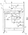
- Fig. 1 shows a block diagram of an embodiment of a voltage converter circuit 10 according to the present invention.
- the voltage converter circuit 10 for pulsed supply of energy to an energy store 12, based on an input voltage VDD, which is applied to an input 14 of the voltage converter circuit 10, has an energy store 12 for storing energy and a switch arrangement 15 with a control terminal 100a.
- the switch arrangement 15 is coupled to the energy store 12 in order to supply energy to the energy store in a switchable manner as a function of a control signal applied to the control terminal.
- Voltage transformer circuit 10 further includes a feedback circuit 20 configured to provide a feedback signal in response to a change in energy stored in energy storage 12 or in dependence on an amount of energy stored in energy storage.
- the feedback circuit 20 further includes a switchable coupling element or coupler 24 configured to couple the feedback signal to the control terminal 100a of the switch assembly.
- the switchable coupling element 24 is designed to provide a stronger coupling effect in a starting phase of the voltage conversion than after the starting phase.
- Fig. 1 based on the realization that in a starting phase, so if the voltage transformer a lower voltage at the input of the voltage converter can be available than after the start phase. With the aid of the switchable coupling element of the feedback circuit, a stronger feedback can therefore be provided in the starting phase of the voltage conversion, so that a control signal can be coupled to the control terminal of the switch arrangement even at a low input voltage and energy can be supplied to the energy store in a switchable manner. After the start-up phase, a higher or a higher voltage can be present at the input of the voltage converter circuit, and the coupling effect of the switchable coupling element can be reduced so as to avoid, for example, overmodulation of the switch arrangement.
- the switchable coupling element 24 can have two capacitors (24a, 24c) connected in parallel (FIG. Fig.2 ), wherein one of the capacitances is switchable via the starting aid switch to the control connection 24b '.
- the capacitance of the switchable coupling element 24 can then be increased by closing a start assist switch 24b in order to increase a capacitive coupling and in an operating phase, after the start phase, the start assist switch can be opened and the capacitive coupling thus reduced become.
- Fig. 2 shows a circuit diagram for a voltage converter according to another embodiment of the present invention.
- the voltage converter may be a self-oscillating voltage converter which has no active drive circuit of the switching transistor or switch 100.
- the voltage converter circuit 10 with the input 14, to which an input voltage VDD can be applied, has an energy store 12.
- At the input 14 of the voltage converter circuit may be present an input voltage VDD, which is determined by the potential difference of the reference potential VSS and the supply potential, which is applied to the input 14, is given.
- an input capacitor C 1 bw. 18 coupled.
- the energy storage 12 may be formed as an inductive element, for example as an (induction) coil.
- This induction coil 12 may be inductively coupled to an inductive element 22 of the feedback circuit 20.
- the induction coil 12 and the inductive element 22 may be part of a transformer, for example.
- a time-varying current flow through the coil 12 or L 1 generates an induction voltage in the inductive element 22 or L 2 .
- the inductive element 12 may be coupled to the input 14 and may provide a higher voltage than an input voltage at a terminal connected to a switchable coupling element 24 by the induced induction voltage. The induced voltage can thus serve as the feedback signal.
- the feedback circuit 20 further includes a switchable coupling element 24.
- the switchable coupling element which can serve as a jump start for the voltage converter, comprise a switchable capacitive coupling element with two capacitors C 4 and C 3 connected in parallel.
- the capacitor C 4 can be switched on by means of the start assist switch 24b, which is embodied here as an n-type JFET transistor, during a start phase. Its capacity thus contributes effectively to the total capacitance of the switchable capacitive coupling element 24, while it does not contribute or only reduced to the total capacity and thus to the coupling after the start phase by opening the switch 100 or blocking the JFETs.
- a feedback from the energy store 12 to the control terminal 100a of the switch 100 in the starting phase is stronger than after the end of the starting phase, and also after the starting phase reduced feedback exists.
- the switch 100 is already active at a voltage applied to the input start voltage, which is smaller than a turn-on voltage of the switch 100, to supply energy to the energy storage.
- the starting voltage from which the voltage converter circuit starts in order to convert an input voltage applied to the input can thus be smaller in magnitude than a threshold or switch-on voltage of the switch or transistor 100. However, this is not absolutely necessary.
- the switch arrangement 15 has a switch 100 which is designed, for example, as an n-channel MOSFET.
- a control terminal 100a of the switch 100 is connected to the switchable coupling element 24 or coupled via the switchable coupling element 24 to the energy store 12.
- the control connection 100a is activated in such a way that energy is supplied to the energy store 12 in a clocked manner or in a switchable manner, which is then opened in a phase in which the switch 100 is open via the diode D3 or 29 the Harmonkondenstor 38 and C 5 is transmitted.
- the then reversely poled diode D 3 prevents a "reflux" of the energy stored on the output capacitor C 5 , eg charge, during the phase in which the switch 100 is closed and a current through the coil 12 from the supply potential to the reference potential VSS is built. Due to the changing current through the coil, a voltage is then induced in the inductive element 22.
- the feedback circuit 20 in this embodiment further comprises a capacitive element 26 and C 2 and a resistive element 25 a and R 2, respectively.
- a first side of this resistor capacitance element (RC element of C 2 and R 2 ) is connected via a diode D4 with the switchable coupling element 24 and a terminal of the induction coil 22 and L 2 .
- a second side of the resistance capacity member is connected to the reference potential VSS. If the voltage converter circuit oscillates, the capacitor C 2 is negatively charged by the voltage supplied by the inductive element via the diode D4. The voltage building up on the capacitor C 2 can be so great after the start phase, that is to say during the operating phase, that the start assist switch 24b is permanently open or that in this exemplary embodiment the JFET 24b is permanently blocked.
- the input voltage is connected to the switchable coupling element 24 via the resistive element R3.
- the switch 100 can be active from an input voltage VDD which is less than a turn-on voltage of the switch 100 to supply energy to the energy store.
- the voltage converter can already start at a starting voltage, which is applied to the input 14, based on the reference potential VSS and which is smaller than a switch-on or threshold voltage for switching the switch 100, to convert the voltage applied to the input.
- the switch arrangement 15 may include a switch 100 which is designed to supply energy to the energy store in a switchable manner as a function of a control signal applied to the control connection 100a of the switch 100.
- the switch 100 may be, for example, a transistor, for example a field-effect transistor or a bipolar transistor, and the control terminal 100a of the switch arrangement 15 corresponding to a control terminal (gate terminal or base terminal) of the transistor.
- the switch may be, for example, a metal oxide semiconductor field effect transistor (MOSFET), or a junction field effect transistor.
- MOSFET metal oxide semiconductor field effect transistor
- the energy storage 12 may be formed in embodiments as a coil, for storing or latching magnetic field energy
- the feedback circuit 20 may include an inductive element 22, for example, also a coil having.
- the inductive element 22 may be magnetically coupled to the coil 12 such that a voltage is induced in the inductive element 22 by a change in the energy stored in the coil 12.
- This induced voltage may be coupled to the control terminal 100a of the switch 100 according to embodiments by a switchable capacitive element 24, which may be part of the feedback circuit 20.
- the switchable capacitive element can be designed to provide a stronger coupling effect between the inductive element 22 and the control terminal 100a in a starting phase than after the starting phase. In other words, the switchable coupling element can serve as jump start for the oscillation of the voltage converter 10.
- the switchable capacitive element 24 may include a start assist switch 24b which is connected such that the switchable capacitive element 24 provides a stronger coupling effect in the starting phase than after the starting phase.
- the starting aid switch 24b may, for example, be a self-conducting transistor which is already in its conducting state with small voltages.
- the start assist switch 24b may thus be, for example, a junction field effect transistor (JFET).
- the energy storage as already mentioned above, be formed as a coil 12, which is inductive with an inductive element 22 of the feedback circuit 20 is coupled.
- a self-oscillating oscillation in the voltage converter circuit can be excited, which enables clocked transmission of energy to an output side of the voltage converter.
- the voltage converter circuit may be configured such that the energy store 12 is coupled to an output capacitance 28 via a rectifier 38, for example a diode.
- a charge transferred from the energy store can be stored on the output capacitance 28, so that depending on the transmitted charge, an output voltage can be provided which can be higher than an input voltage VDD applied to the input 14 of the voltage converter circuit 10.
- the energy store can be coupled to the feedback circuit 20 in such a way that a feedback signal is produced in response to a change in the energy stored in the energy store or in dependence on a quantity of the energy stored in the energy store, which excites the voltage converter circuit to self-oscillating oscillations ,
- the feedback signal may be coupled to the control terminal of the switch 100, thereby providing a control signal for energizing the energy storage in a switchable manner.
- the start assist switch 24b may be formed as a junction field effect transistor whose control terminal 24b 'is coupled to the energy storage 12 such that the start assist switch 24b is active in the startup phase to effect a stronger coupling than after the startup phase , It is also possible that the start assist switch 24b is connected such that a coupling effect of the switchable capacitive element 24 on the control terminal 100a of the switch 100, as a transistor is formed during the startup phase is changed periodically.
- the voltage converting circuit 10 may further include a capacitive element 26 coupled to the switch 100 and configured to establish a potential depending on a change in the energy in the energy storage 12 or the amount of energy in the energy storage to turn off the start assist switch 24b.
- a capacitive element 26 coupled to the switch 100 and configured to establish a potential depending on a change in the energy in the energy storage 12 or the amount of energy in the energy storage to turn off the start assist switch 24b.
- a capacitive element 26 coupled to the switch 100 and configured to establish a potential depending on a change in the energy in the energy storage 12 or the amount of energy in the energy storage to turn off the start assist switch 24b.
- the start assist switch is designed as a transistor, that is, the electrical resistance between the source and the drain of the transistor is increased and a current flow between the two load paths (drain and source). reduced or stopped - so the transistor locks.
- the switch assembly 15 described above may include a first switch 13 and a second switch 17 (see FIG Fig. 3 . 4 . 5 ), which are connected in parallel with each other.
- the first switch 13 may have a smaller turn-on voltage than the second switch 17.
- a control terminal 13a of the first switch 13 may be connected such that the first switch is active in a starting phase of the voltage converter circuit, ie is closed in order to supply energy to the energy store ,
- a control terminal 17a of the second switch 17 can be connected so that the second switch is active after the start phase to the energy storage 12 in clocked Way to supply energy.
- the feedback circuit 20 also includes a switchable coupling element 24 configured to couple the feedback signal, for example, from the inductive element 22 to the control terminal 17a of the second switch 17.
- the switchable coupling element 24 is designed to provide a stronger coupling effect in a starting phase than after the starting phase.
- the function of the voltage converter 10, which in the embodiment in Fig. 2 can be described as follows.
- the n-type JFET T 4 or 24 b is initially conductive, since its gate-source voltage is approximately equal to zero.
- This causes a parallel connection of the capacitor C 4 or 24a and the orders of magnitude smaller capacitor C 3 and 24c.
- a capacitance of the switchable feedback capacitor C 4 may, for example, be at least 10 times greater than a capacitance of the permanently active feedback capacitor C 3 .
- the capacitor C 2 is negatively charged via the diode D 4 . This voltage becomes so high during static operation that the JFET 24b remains locked in static operation at any time.
- the capacitor C 4 is ineffective and only the capacitor C 3 is active.
- C 3 practically forms a voltage divider with the parasitic capacitances at the gate terminal of the transistor T 1 and 100, respectively.
- the capacitance value of the capacitor C 3 can be optimized so that the switching edges on the transistor T 1 can be kept low.
- the resistor R 2 or 25a ensures that the capacitor C 2 or 26 is discharged again after switching off the voltage converter, and thus the JFET T 4 is again conductive when the converter 10 is restarted.
- the two coils 12 and 22 of the transformer of the DC-DC converter for example, together, for example, have an ER9.5 core of the ferrite N87.
- the turns of the two coils L 1 and L 2 in this example is 1: 8.
- the JFET PMBF4393 Philips company can be used, which has according to its data sheet a pinch-off voltage between -3.0 V and -0.5 V.
- the switching transistor T 1 or 100 may be, for example, the MOSFET NDS335N Fairchild.
- the threshold voltage of this MOSFET is in accordance with its data sheet at about 0.7 V.
- the capacitance values of the capacitors C 3 and C 4 may, for example, 320 pF and 22 nF, respectively.
- the voltage converter can already start at 520 mV.
- the circuit were operated solely with the capacitor C 3 , ie without the aid of the capacitor C 4 , the converter only started at a starting voltage of 680 mV.
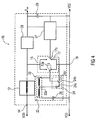
- Fig. 3 shows a block diagram of another embodiment of a voltage converter circuit 10 according to the present invention.
- the voltage converter circuit 10 for pulsed supply of energy to an energy store based on an input voltage VDD, which is applied to an input 14 of the voltage converter circuit 10, has an energy store 12 for storing energy and a switch arrangement 15, which is coupled to the energy store 12.
- the switch arrangement 15 has a first switch 13 and a second switch 17, which are connected in parallel to one another and are coupled to the energy store.
- the first switch 13 has a smaller turn on than the second switch 17.
- a control terminal 13a of the first switch is connected so that the first switch is active in a start phase of the voltage converter circuit to supply energy to the energy store.
- a control terminal 17a of the second switch 17 is connected so that the second switch is active after the start-up phase to supply energy to the energy store in a clocked manner.
- the energy storage 12 may be, for example, an inductive element, ie z. B. an induction coil act.
- the first switch 13 can then be active, ie closed, so that a time-variable current, that is, for example, a time-increasing current through the coil from the input 14 to a reference potential VSS flows and thus an energy stored in a magnetic field of the coil increases.
- the control connection 17a of the second switch 17 can then be activated on the basis of a corresponding connection such that the second switch 17 is closed and opened in a clocked manner.
- magnetic field energy can also be supplied to this coil 12 by means of a variable current flow through the coil 12.
- the current can flow with closed first or second switch to the reference potential VSS, which may be, for example, a ground potential.
- it may be, for example, a voltage converter circuit with a capacitive energy storage 12.
- This voltage converter circuit can then be integrated, for example, in a charge pump.
- the voltage converter circuit may thus be, for example, an inductive converter circuit or a capacitive voltage converter circuit. If the voltage converter circuit includes a coupled coil transformer, some embodiments of the present invention may also be a DC-DC converter.
- Fig. 4 shows a further block diagram of an embodiment of a voltage converter circuit 10.
- the voltage converter circuit 10 has an energy storage 12, which may be designed as an inductive element, for example, a first coil, or first induction coil.
- This first induction coil 12 can be inductive with an inductive element 22 of a feedback circuit 20 be coupled. Ie. by a change in the energy stored in the induction coil, that is, when a time-varying current flows through the induction coil 12, a voltage is induced in the inductive element 22.
- the feedback circuit 20 may further include a switchable coupling element 24, such as a switchable capacitive element, configured to provide a stronger coupling action between the inductive element 22 and the control terminal 17a of the second switch 17 in a starting phase than after the starting phase.
- the feedback circuit 20 can be designed to couple a voltage to the control terminal 17a of the second switch 17 via the capacitive element 24, so that the second switch 17 is active or driven after the start phase to the energy store 12, ie the induction coil to supply energy in a timed manner. Ie. for example, by applying a voltage coupled via the capacitive element 24 to the control terminal 17a of the second switch, the second switch can be closed, so that a time-variable current flow through the coil 12 to the reference potential VSS takes place, whereby a magnetic energy is supplied to the coil 12 ,
- the switchable coupling element e.g.
- the switchable capacitive element 24 of the feedback circuit 20 may be a capacitor 24a connected in series with a third switch 24b.
- the control terminal of the third switch 24b may be connected so that the switch is closed during the starting phase so as to achieve a stronger coupling via the capacitor 24a to the control terminal 17a of the second switch 17, than after a starting phase in which the third switch 24b is open.
- the capacitor 24 a separates the DC component of the induced voltage from the control connection 17 a of the second switch 17.
- the feedback circuit 20 may be configured such that a terminal of the inductive element 22 is connected to a further capacitive element 26 of the feedback circuit 20.
- the capacitive element 26 may be designed to build up a potential in the starting phase by an induced voltage on the inductive element 22, compared to the reference potential VSS, so that the control terminal 13a of the first switch 13, which is also coupled to the inductive element 22 , Is so controlled that in the start phase, a supply of energy to the induction coil 12 by periodic partial opening and closing of the first switch 13, is reduced until after the start phase, a potential applied to the capacitive element 26, so that the supply of energy to the energy storage 12 by opening the first switch 13 is completed.
- the first, the second and the third switch may be, for example, transistors.
- the first switch 13 may be, for example, a junction field-effect transistor or "junction" field-effect transistor (JFET), for example a self-conducting transistor which is already turned on at a drive voltage of 0 V, ie electrically conductive , is.
- the second switch may, for example, be a metal oxide semiconductor field effect transistor (MOSFET), for example an NMOS transistor or also a PMOS transistor.
- the third switch 24b may again be a self-conducting JFET transistor.
- the first transistor 13 may therefore be a self-conducting transistor which is already live at a control voltage or gate voltage of 0V
- the second switch 17 may be, for example, a MOSFET with a turn-on voltage which is higher than the turn-on
- only the first transistor, for example the JFET 13 can be initially active since a voltage applied to the input 14 can be low. Because the JFET is a self-conducting device is, but can already flow from an input voltage just above 0V on the inductor 12, so the energy storage, a current.
- a current across the induction coil 12 at the start-up of the converter increases, so that in the induction coil 12, a time-varying current flows and thereby in the inductive element 22, a voltage is induced.
- a negative current in the inductive element 22, which may also be formed as a coil can be induced, so that the capacitive element 26 is charged with a low negative voltage. Since a PN junction to the reference potential VSS is given at the control terminal 13a of the JFET transistor 13, a small negative voltage may be formed on the capacitive element 26 over time due to the diode rectification effect.
- the first transistor 13 If the voltage across the capacitive element 26 falls below a certain negative value, that is, for example, lower than a turn-on voltage of the first switch or the first transistor 13, the first transistor 13 is no longer turned on and the second switch 17 or the MOSFET is to the switching transistor. After the start phase, therefore, the second switch or the MOSFET transistor 17 takes over the pulsed supply of energy to the energy store 12.
- the energy storage 12 may be coupled to the feedback circuit 20 so that a self-oscillating oscillation of the voltage conversion circuit may be excited in response to a change in the energy stored in the energy storage 12.
- the energy store may, for example, be an induction coil, which is inductively coupled to the feedback circuit, so that a self-oscillating oscillation of the voltage converter circuit is excited as a function of a change in the current flowing in the induction coil.
- the DC-DC voltage converter circuit described here is therefore in basic embodiments a self-oscillating converter, i. the switches or switching transistors are not driven via an active circuit, but only via coupled coils of a transformer.
- the energy store 12 may be coupled to a feedback circuit 20 in such a way that, depending on a change in the energy stored in the energy store or in response to a quantity of the energy stored in the energy storage, a feedback signal is produced which excites the voltage conversion circuit to self-oscillating oscillations.
- the feedback circuit 20 may include a resistive element 25a and a capacitive element 26 such that the frequency of the self-oscillating oscillation for pulsed supply of energy to the energy storage depends, inter alia, on an RC time constant of the feedback circuit 20.
- the voltage converter circuit for clocking energy to an energy store may also include a control loop 27 configured to control the frequency or duty cycle of supplying energy to the energy store after the startup phase.
- the control loop 27 can be coupled to a control connection 17a of the second switch 17.
- the voltage converter circuit may be formed so that the energy storage device 12 via a rectifying element, so z. B. a diode is coupled to an output capacitance 28.
- An output voltage V out can then be made available at the output capacitance 28 as a function of a charge transferred from the energy store 12.
- This output voltage may be higher in embodiments than an input voltage applied to the input of the voltage converter circuit.
- the rectifier element 29 may be a switched rectification element, that is, for example, a diode connected in parallel with a switch.
- the switch may be a transistor whose control terminal is connected in a predetermined manner.
- the transfer of charges to the output capacitance 28 may be performed such that after the startup phase the energy storage 12 is clocked in Way is supplied by closing the second switch 17 energy. Charges may be transferred from the energy storage to the output capacity 28 in a clocked manner. Ie. After the start phase, energy is temporarily stored in the energy store 12 during the phase in which the switch 17 is closed. In the (clocked) phases in which the switch 17 is opened, this cached energy or charge is transmitted via the rectifying element 29 to the output capacitance 28. The charges are thus "pumped" to the output capacitance in a clocked manner opposite to the clocked manner, ie for example when the switch 17 is open. There can then form an output voltage V out at the output capacitance 28, which may differ in magnitude with respect to their voltage value of the input voltage.
- the control of this pulsed supply of energy in the energy storage 12 and in the opposite phases, the transfer of this cached energy to the output capacity 28 can be supported or enabled by the control loop 27.
- the output capacitor 28 acts as a second energy store at the output of the voltage converter circuit, so that an output voltage is available which differs from the input voltage.
- the control loop 27 may be coupled to a control terminal of the second switch 17, in response to a load on the output capacitance 28 a frequency for the pulsed supply of energy to the energy storage 12 and for the clocked feeding opposite clocked transfer of charges from the Energy storage to the output capacity 28 to control.
- the control loop may be configured such that the frequency for pulsed supply of energy and for transferring charges to the output capacitance 28, the higher the load on the output capacitance is. Ie.
- the frequency of the voltage conversion can be changed.
- the Fig. 5 shows the circuit diagram of a voltage converter circuit according to another embodiment of the present invention.
- the voltage converter circuit 10 for pulsed supply of energy to an energy store based on an input voltage has in this embodiment, an energy storage 12, which is designed as an inductive element, that is, for example, as a first coil.
- At the input of the voltage converter circuit 14 is connected to an input voltage VDD, which is connected to the energy storage 12.
- an input capacitor C 1 18 may be coupled in this embodiment.
- the energy storage 12 is connected in this embodiment with the switch assembly 15.
- the switch arrangement 15 has a normally-on first JFET transistor T 1 or 13.
- the switch assembly 15 also includes a second MOSFET transistor T 2 and 17, for example, here an NMOS transistor which is connected in parallel with the JFET transistor T. 1
- the parallel-connected transistors T 1 and T 2 are coupled to the energy store 12 and coupled to a reference potential VSS 19.
- the normally-on JFET transistor T 1 or 13, which acts as a first switch, has a smaller turn-on than the NMOS transistor T 2 and 17, for example.
- the JFET transistor 13 a turn-on voltage or a Einschaltschwellschreib of 0V.
- the energy store 12 is magnetically or inductively coupled in the embodiment shown with an inductive element 22 to the feedback circuit.
- the inductive element 22 may in this embodiment of two induction coils L 3 and L 2 exist.
- the inductive element 22 can be connected to a switchable capacitive element 24 via a tap 22a, which is connected between the second induction coil L 2 and the third induction coil L 3 .
- the switchable capacitive element 24 consists in this embodiment of two parallel-connected capacitors C3 and 24c and C4 and 24a.
- the branch with the capacitor 24 or C 4 has a JFET transistor 24b and T 4 , so that depending on the wiring of the capacitor 24b, the total capacitance of the capacitive element 24 can be increased.
- the JFET T 4 24b can then be connected so that in a start phase of the voltage converter circuit, the total capacitance of the capacitive element 24 is increased.
- the capacitive element 24 is in this embodiment, therefore, on the one hand connected to the tap 22a of the inductive element 22 and on the other hand to the control terminal 17a of the NMOS transistor T 2nd
- the feedback circuit 20 further comprises a capacitive element 26 and C 2 and a resistive element 25 a and R 3, respectively.
- This resistor capacitance element (RC element of C 2 and R 3 ) is connected to a terminal of the second inductor L 2 and the reference potential VSS.
- the voltage converter circuit 10 described in this embodiment can be, for example, a DC-DC converter, which is a self-oscillating converter in its basic concept. That is, the switching transistors of the voltage converter circuit need not be controlled via an active circuit, but are driven only via coupled coils of a transformer, so that there is a self-oscillating oscillation of the DC-DC converter.
- the JFET T 1 13 When an input voltage VDD is applied to an input 14, the JFET T 1 13 initially operates in a startup phase. Since the JFET is a self-conducting component, a current builds up already starting at an input voltage above 0V in the inductance L 1 , ie the energy store 12 of the transformer on. Since the input voltage increases during startup of the converter, the current through the induction coil L 1 , so that in the second induction coil L 2 and the third induction coil L 3, a voltage is induced, and the transducer begins to oscillate. As soon as the voltage at the tap 22a between the second induction coil L 2 and the third induction coil L 3 of the transformer is large enough, the MOSFET transistor T 2 or 17 switches on and takes over the current conduction in the voltage converter.
- the JFET 13 in a start-up phase, the JFET 13 is first active, ie, a current flows through the first coil L 1 via the JFET to the reference potential VSS 19. This couples a voltage to the feedback circuit 20 via the inductive element 22.
- the capacitor 24a can be switched to the capacitance of the capacitor 24c by connecting the inductive element 22 with the JFET 24b, the capacitive element 24, so that in the start phase, a stronger coupling effect on the control terminal 17a of the second transistor 17th after a start-up phase in which the JFET 24b is turned off, so that the total capacitance of the capacitive element 24 is reduced.
- a negative current is induced in the inductive element 22 in this exemplary embodiment, so that a small negative voltage is applied to the capacitive element 26 because of the PN junction at the gate terminal 13a of the barrier layer.
- the source side is connected to the reference potential VSS builds.
- the reference potential VSS may be, for example, a ground or ground potential.
- the current in the primary coil L 1 or 12 is then For example, constant when the input voltage is stable or constant. As a result, the current flow through the primary coil 12 and L 1 is also constant and no voltage is induced in the secondary coils L 2 and L 3 .
- ⁇ can be of the order of microseconds, and therefore a high negative voltage can be induced in the inductive element 22 until the current through the first coil 12 reaches its maximum value.
- the control terminal 13a of the JFET 13 is coupled to the capacitive element 26 and the JFET 13 may be turned off. This causes the current flow through the first coil 12 to decrease until the current flow drops, for example, back to zero. Then the cycle can start anew.
- the voltage across the capacitive element 26 is less than the turn-on threshold voltage of the JEFT, the JFET is no longer turned on and the second transistor 17, for example the NMOS T 2 , becomes the switching transistor through which a main current flows.
- the capacitive element 26 can be charged more negatively and an output capacitance 28 can be charged via the diode D 3 .
- the voltage converter can be excited to self-oscillating oscillations.
- a voltage can be transmitted to the control terminal 17a of the MOSFET transistor 17, so that it takes over the current conduction upon reaching its turn-on voltage.
- the MOSFET T 2 turns on and takes over the power supply.
- the capacitive element C 2 is charged negatively, so that in the steady state, ie after the start phase, at this a constant negative voltage is applied and the JFET T 1 is turned off.
- the capacitor 24c and the capacitor 24a separate the DC component at the tap 22a from the gate terminal of the MOSFET T 2 .
- an operating frequency of the voltage converter circuit is then substantially, after the starting phase, from the capacitor C 3 and 24c and 25b and the resistive element R. 3 certainly.
- the operating frequency may be further influenced by a control loop 27, as illustrated below.
- the control loop 27 may be configured to control the frequency of the clocked conversion of an input voltage to an output voltage.
- the control loop 27 may be coupled to the control or gate terminal 17a of the MOSFET transistor 17. That is, the frequency of supplying power to the first inductor 12 and transferring energy or charge to an output capacitance 28 of the voltage converter 10 may be controlled by the control loop 27.
- the control loop 27 is designed in this embodiment, that in response to a load on the output capacitance 28, a frequency for the clocked coupling and for transferring charge from the first coil to the output capacitor 28 controlled becomes.
- the gate terminal 17a may be connected to a branch for a negative voltage limit 27a and a branch for a positive voltage limit 27b.
- the branch for the negative voltage limit 27a may comprise a diode D 1 or 30, which is connected in series with a resistive element 31 or R 1 to the reference potential VSS.
- the branch for a positive voltage limitation 27b may be arranged.
- This branch has a diode 32, which is connected in series with a transistor 33 against the reference potential.
- a control terminal or a control gate 33a of the transistor 33 T 7 can be controlled via a variable resistor 34 R 6 , so for example a potentiometer, which is connected via a Zener diode 35 parallel to the output capacitance 28.
- the resistance of the potentiometer 34 or a voltage divider effect of the potentiometer 34 can be changed and thus the gate voltage at the transistor 33.
- a time constant of a gate drive signal of the MOSFET T 2 can be adjusted.
- the frequency or a duty ratio of the opening and closing of the transistor 17 and thus the pulsed supply of energy or the transfer of charges to the output capacitance 28 can be adjusted.
- the control loop 27 may thus have a diode D 7 , a transistor T 7 , a Zener diode D 6 and a voltage divider R 6 .
- this control loop the on-time of the switching transistor T 2 can be controlled.
- the higher the load the lower the operating frequency.
- the Zener diodes 36 and 37 are protective diodes, which prevent, for example, in the event of a fault, that the MOSFET T 2 or 17 gets unduly high voltages at its control or gate terminal.
- the resistor 31 or R 1 serves as an additional jump start for the converter.
- a switchable rectifier 29 can be arranged between the first induction coil 12 and the output capacitance 28.
- the switchable rectifier 29 may have a diode 38 which is arranged parallel to a transistor T 3 or 39, which is connected via a further control circuit 40 and is driven.
- a transistor 39 is connected in parallel to the diode D 3 or 38 of the switchable rectifier 29, which takes over the power supply, if the diode would normally conduct. This can be realized for example via a drive circuit 40.
- the controllable transistor 39 may be, for example, a PMOS transistor having a sufficient dead time, that is, a sufficient time in which it is open, so that there is no overlap of the PMOS transistor T 3 or 39 and the second MOSFET T 2 can come.
- a high efficiency of the voltage converter circuit can be achieved by a suitable design of the transformer, so the coupled coils 12 and 22.
- the secondary side (L 2 and L 3 ) may have a tap 22 a, in order to optimally control the MOSFET transistor T 2 , that is to minimize switching losses and yet to ensure low starting voltages.
- the inductance of the winding of the induction coil 12 or L 1 is selected as large as possible in some embodiments, so that an open-circuit current of the converter can be kept low in relation to the maximum input current.
- core materials can be used which have a high absolute magnetic permeability ⁇ .
- the absolute magnetic permeability in some embodiments, may be greater than 6 x 10 -5 H / m, for example, greater than 6.28 x 10 -5 H / m, which corresponds to a relative magnetic permeability ⁇ r of 50.
- the circuit described above for a DC-DC boost converter may be constructed exclusively of discrete components.
- all of the corresponding components can be consistently available as Surface Mounted Devices (SMD).
- SMD Surface Mounted Devices
- an ER9.5 core made of ferrite material N87 which still has small dimensions in relation to the overall circuit, can be used for the transformer, that is to say the coils for inductive coupling. So that the converter, so the voltage converter circuit at low input voltages of z. B. 60 mV starts, on the one hand, the winding or winding ratio of the first induction coil L 1 or 12 to the second induction coil L 2 and the third induction coil L 3 is about 1: 8.5 to choose.
- the winding ratio can, for example, depending on the turn-on voltage of the JFET T 1 and the transistor T 3rd also between 1: 4 and 1:25.
- the JFET T 1 has a low pinch-off voltage of approximately 1.2V. It is important to ensure that the maximum gate-source voltage is sufficiently high.
- the JFET PMBF4393 Philips company can be used. According to its data sheet, this has a pinch-off voltage between -3.0 V and -0.5 V and a maximum permissible gate-source voltage of 40 V.
- the MOSFET BSH105 from Philips can be used as the switching transistor T 2 . The threshold voltage of this switching transistor is about 0.6V. If the specified switching transistors are used, it makes sense in some embodiments to dimension the second induction coil L 2 and the third induction coil L 3 exactly the same size.
- the protection circuit may include a protective circuit which is coupled to the control terminal 17a of the second switch 17 in order to protect the control terminal of the second switch against an overvoltage.
- the protection circuit can be two oppositely coupled or polarized zener diodes 36 and 37, which are connected, for example, in the manner shown.
- control terminal 17a of the second switch 17 may be coupled to a control loop or loop 27, the control loop being configured to adjust the frequency of the pulsed supply of energy to the energy store and a transfer of charge from the energy store to one to control the output coupled to the energy storage capacity 28.
- the control loop 27 can for this purpose have a positive and a negative current limit or voltage limitation, wherein the voltage limitation as a function of a load or in dependence an output voltage, the positive and / or the negative current limit or voltage limit can change so that the turn-on voltage of the second switch 17 is exceeded or exceeded. In other words, the second switch 17 can therefore be switched on and off depending on the load.
- the switch arrangement 15 with the first and second switches connected in parallel to each other can be designed such that the switch arrangement has a switch-on voltage between 0V and 100mV in the starting phase of the voltage conversion or the voltage converter circuit and is active after the start phase via the second switch, so that this Current path has a lower resistance than a current path via the first switch T 1 .
- the first switch may be a normally-on transistor and the second switch may be a normally-off transistor.
- the first switch may be a JFET and the second switch may be a MOSFET.
- the first switch 13 may also be a depletion type N-channel FET while the second switch 17 is an enhancement mode N-channel FET.
- the first switch 17 may, for example, be an N-channel MOSFET having a smaller turn-on voltage or threshold voltage, while the second switch has an N-channel MOSFET having a larger threshold voltage. It is also conceivable, however, that in embodiments transistors with a correspondingly opposite doping are used. Different turn-on voltages can be achieved, for example, by different doping profiles, by differently thick gate oxides or by other design parameters of the field-effect transistors (FET).
- FET field-effect transistors
- the voltage converter circuit may further include a feedback circuit 20 configured to in response to a change in the energy stored in the energy storage 12 or in response to a quantity of energy stored in the energy storage, to provide a feedback signal.
- the feedback circuit 20 may include a switchable coupling element 24 configured to couple the feedback signal to the control terminal 17a of the second switch 17, the switchable coupling element 24 being configured to provide a stronger coupling effect in a starting phase than after the starting phase.
- the switch arrangement 15 can be designed such that in a starting phase the first coil 12 can be coupled to the reference potential VSS via the first switch or via the first transistor 13, so that a current flow through the first coil 12 can take place and a voltage in the feedback circuit 20 can be induced.
- a current flow through the coil can be generated or made possible by closing the second switch 17, so that a voltage can be induced in the feedback circuit 20 .
- the voltage converter circuit can be designed as a voltage converter, which provides an output voltage V out at an output.
- the voltage converter may have an output capacitor for temporarily storing charge, ie energy.
- the voltage converter can thus be designed so that the second switch 17 after the start phase allows a clocked coupling of the coil with the reference potential, whereby a current flows through the coil, which supplies magnetic energy to the coil, which then set in one of the clocked coupling clocked phase is transferred in the form of charges from the coil 12 to the output capacitor 28.
- a rectifying Element such as a diode or a switchable rectifying element 29 may be coupled.
- the output capacitor 28 can be charged via the switchable rectifying element 29.
- the feedback circuit 20 may be configured to use the capacitive element 26 and C 2 , respectively, to turn off the first switch or junction FET. That is, if a voltage across the capacitive element 26 is less than a turn-on or threshold voltage of the first switch T 1 and the first junction FETs, this is switched off permanently, and the second transistor T 2 , for example, an NMOS transistor can become the active switching transistor. The capacitive element 26 can then continue to charge negatively.
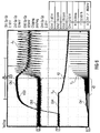
- Fig. 6 the measured current / voltage characteristics at different measuring points of the voltage converter circuit are off Fig. 5 shown.
- the time in milliseconds is plotted on the x-axis of the graph, with an interval equal to 4ms.
- the input voltage VDD is shown, the current through the second switch I T2 and the voltage V L1 to the first coil 12 and the voltage V C2 to the capacitive element 26 of the feedback circuit 20.
- the diagram are current and Voltage values starting with the start phase until after the start phase, ie in the operating phase of the clocked conversion of the input voltage.
- the input voltage only increases after switching on for a certain time, so that in this time a time-variable current can flow via the electrically conductive first transistor T 1 to the reference potential, so that a voltage in the feedback circuit 24 can be induced and, as described above and in the measurement curve V C2 can be seen, builds on the capacitive element 26, a negative voltage.
- This negative voltage results after the input voltage VDD has become constant or a time variation of the current through the first coil has become sufficiently small, to the fact that at the gate terminal 13a of the first transistor T 1, a negative potential from the capacitive element 26 is applied and the first transistor is turned off.
- Fig. 7 shows the measured curves of a control or gate voltage V GT2, the current I T2 in the current-carrying channel of the second transistor, and a current through the diode D3 which is shown in the curve I D3. Furthermore, the output voltage V out , which is available at the output capacitance 28, is shown.
- the time scale for these measurements is how the Fig. 7 it can be seen, 400 ⁇ s per interval unit.
- the current and voltage values in Fig. 7 are in the starting phase, in which the second transistor T 2 takes over the power supply, shown. Accordingly, the output voltage V out builds up only gradually. In the different measuring curves, the clocked conversion is clearly visible.
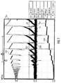
- Fig. 8 shows further measurements of current and voltage at different points of the voltage converter circuit Fig. 5 during the operating phase.
- the temporal resolution for these measurements is 100 ⁇ s per time interval.
- the voltage converter circuit now operates periodically in the operating phase with an operating frequency which can be set, as stated above.
- the voltage at the control terminal of the first transistor T 1 is shown in curve V GT1 and the voltage at the control terminal of the second transistor T 2 is shown in the curve V GT2 .
- the corresponding current through the second transistor T 2 and the corresponding voltage across the first coil 12 have the same periodicity.
- the voltage at the first coil L 1 correspondingly increases at the times when the current flow through the second transistor is interrupted.
- the charge can now be transferred to the output capacitance via the serially coupled switchable rectifier 29. That is, the threshold voltage the diode D 3 of the switchable rectifier 29 is exceeded and the diode turns on.
- a transistor can now be connected in parallel with the diode D 3, which transistor takes over the current conduction if the diode would normally conduct. Since the transistor has a lower on-resistance, ie a low resistance in the on state, than the diode, the efficiency of the voltage converter circuit can be increased by this measure.
- Fig. 9 shows further current or voltage measuring curves at different measuring points of the voltage transformer in Fig. 5 ,
- the current / voltage curves were again measured during the pulsed operating phase, ie after the starting phase.
- the output voltage V out now has an approximately constant value.
- the output capacitance 28 is reduced at the instants at which the second transistor T 2 is turned off, thus the gate voltage V GT2 supplied charge from the first coil 12, so that the output voltage easily increases again. This can be seen from the fact that in the phase in which the current I T2 decreases through the transistor, the current I D3 flows through the diode D 3 to the output capacitance 28.
- both the first switch 13 and the second switch 17 may be active.
- both the control terminal of the first transistor and the control terminal of the second transistor may be driven to turn on the transistors.
- the second transistor in this case takes on a main current flow due to its lower on-resistance.
- a current flow through the second transistor should be at least five times as large as that through the first transistor.
- the present invention also provides a method for pulsed supply of energy to an energy storage based on an input voltage applied to an input of a voltage converter circuit.
- the method has, as in the block diagram in Fig. 10 schematically illustrated a step of supplying 80 energy to the energy storage of the voltage converter circuit in a start-up phase, by activating a first switch, wherein the first switch has a smaller threshold Einschwaltwood than the second switch.
- the method further comprises supplying energy in clocked fashion to the energy storage of the voltage converter circuit after the startup phase by activating the second switch.
- the second switch which is connected in parallel with the first switch, has a larger turn-on voltage than the first switch.
- Activating the second switch may include coupling a feedback signal to the control port of the second switch via a coupling in the startup phase. After the startup phase, the method may include decreasing the coupling.
- the clocked supply 85 of the energy can be performed, for example, so that the voltage converter or the Voltage converter circuit is excited to self-oscillating oscillations, so that the first and / or the second switch is periodically switched off and on and so that thereby energy is supplied to the energy storage.
- the energy store may be, for example, an induction coil.
- a time-varying current flow in the induction coil can be caused, which is cyclically interrupted, for example, and which causes an intermediate storage of a corresponding magnetic energy in the form of a magnetic field in the induction coil.
- the energy storage can also be considered as a buffer.
- the pulsed supply of energy to the energy stores 85 can also include transfers of charges in the phases clocked in opposite phases to the clocked phases, to a second energy store, for example to the output capacitor of the voltage converter.
- the transfer of charges may take place offset in time from the clocked supply, for example in such a way that the transfer of charges and the clocked supply occur alternately or temporally non-overlapping.
- the clocked supply of energy to the energy storage or of energy to the output capacitor can be performed according to a further embodiment so that the frequency for this pulsed process is adjustable by a load on the output capacitor.
- the supply of energy 80 and 85 to the energy store may be performed by feedbacking between the energy in the energy store or by an amount of energy in the energy store the first and the second switch and the energy storage is performed, so that a self-oscillating oscillation in the voltage converter circuit can cause.
- the method of pulsed supply of energy may be performed such that the supply 80 of energy to the energy storage of the voltage converter circuit is feasible at an input voltage that is less than 300mV in magnitude or even less than 100mV.
- the method is carried out such that in a starting phase, the supply of energy to the energy storage with the first transistor, which has a lower turn-on voltage than the second transistor is performed, and that after the start phase, the supply of energy to the energy storage with a second transistor or at least substantially by the second transistor is performed, which has a lower "on" resistance, than the first transistor.
- the first transistor may be formed, for example, as a self-conducting JFET, in which the supply of energy to the energy storage can start from an absolute input voltage greater than 0V or at a gate-source voltage of 0V.
- supplying 110 energy in a switchable manner to the energy store of the voltage converter circuit is dependent from a control signal applied to a control terminal 100a of a switch arrangement.
- a feedback signal is generated by means of a feedback circuit in response to a change in the energy stored in the energy store or as a function of the amount of energy stored in the energy store is provided 120.
- the corresponding feedback circuit includes a switchable coupling element configured to provide the feedback signal to the control terminal 100a of the switch assembly 15 for providing the feedback signal, and wherein the switchable coupling element is configured. in order to provide a stronger coupling effect in a starting phase than after the starting phase.
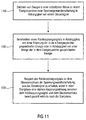
- Fig. 11 shows a flowchart of a further embodiment of the further method for the clocked supply of energy to an energy storage, based on an input voltage VDD, which is applied to an input 14 of a voltage converter circuit 10.
- the further method comprises a step of supplying energy in a switchable manner to the energy store of the voltage converter circuit in response to a control signal.
- the method comprises providing 120 a feedback signal in response to a change in the stored energy in the energy storage or in dependence on an amount of energy stored in the energy storage and coupling 130 of the feedback signal to the control terminal of the switch arrangement to obtain the control signal in which, in a starting phase, a stronger coupling effect between the feedback signal and the control terminal is provided than after the starting phase.
- the presented voltage converter can operate with coupled coils and, for example, start already at an input voltage of 60 mV.
- the voltage converter can already have more than 50 percent efficiency with an output voltage of 2V and an output power of 1mW for small dimensions.
- a high efficiency of the voltage conversion at very low input voltages (below 300 mV) can be achieved.
- the circuit can be constructed from individual components, i. H. it is not necessary to use an integrated circuit. Nevertheless, the component cost can be relatively low.
- the requirement for the transformer to be used, ie the coupled coils can be high, but with an appropriate choice of the components and the core materials, overall small dimensions of the overall arrangement can be achieved.
- the voltage converter circuit or the voltage converter is realized entirely or at least partially in the form of an integrated circuit.
- the voltage converter circuit as a synchronous step-up converter, that is, a boost converter with a feedback loop, which allows to regulate the output voltage during the operating phase, or as a boost converter, may be formed.
- a suitably modified voltage converter circuit is designed as a step-down converter, in which the output voltage is smaller than the input voltage.
- the feedback circuit may comprise a switchable coupling element (24) which may be formed as a switchable capacitive element.
- a second MOSFET transistor T 2 which is connected in parallel with a JFET transistor T 1, serve as a switching element for converting the clocked voltage.
- the parallel connection of both transistors makes it possible, on the one hand, to use a low input voltage for the starting operation of the voltage converter since the first transistor can be self-conducting and a "zero-threshold gate voltage", ie a zero Voltage threshold voltage, and on the other, during the operating phase to have a high efficiency, since the second MOSFET 17 has a low on-resistance (on-resistance) in the on state.
- control loop 27 which is designed to control the frequency or a duty cycle of the supply of energy to the energy store after the start phase of the voltage converter circuit.
- the control loop 27 in the embodiments, in connection with the Fig. 1 and 2 are described, for example, with the control terminal 100a of the switch assembly 15, and be coupled to the control terminal of the switch 100.
- a voltage converter circuit 10 for pulsed supply of energy to an energy store 12, based on an input voltage VDD, which is applied to an input 14 of the voltage converter circuit, could have the following features: an energy store 12; a switch assembly 15, wherein the switch assembly comprises a first switch 13 and a second switch 17, which are connected in parallel to each other, wherein the switch assembly is coupled to the energy storage, wherein the first switch has a smaller amount turn-on than the second switch, wherein a Control terminal 13a of the first switch 13 is connected so that the first switch is active in a start phase of the voltage converter circuit to supply energy to the energy store, and wherein a control terminal 17a of the second switch is connected so that the second switch 17 is active after the start phase for supplying power to the energy storage 12 in a clocked manner; and a feedback circuit 20 configured to provide a feedback signal in response to a change in the energy stored in the energy store 12 or in dependence on an amount of energy stored in the energy store, the feedback circuit 20 having a switchable coupling element 24 configured is to couple the
- the energy store is a coil 12 which is inductively coupled to an inductive element 22 of a feedback circuit 20 so that a self-oscillating oscillation in the voltage converter circuit can be excited in response to a change in the energy stored in the coil.
- the frequency of the self-oscillating oscillation for the pulsed supply of energy to the energy store 12 depends on a resistor-capacitor time constant.
- the energy store is coupled to the feedback circuit 20 so as to produce a feedback signal that self-oscillates the voltage converter circuit in response to a change in the energy stored in the energy store or in dependence on an amount of energy stored in the energy store Excites oscillations.
- control terminal 17a of the second switch 17 is coupled to a control loop 27, which is designed to influence the frequency of the pulsed supply of energy to the energy store 12.
- the energy store is coupled via a switched rectifier 29 to an output capacitance 28, which is designed to provide an output voltage which is higher than an input voltage, depending on a charge transferred from the energy store an input of the voltage converter circuit is applied.
- control terminal 17a of the second switch 17 is connected so that the second switch is active after the start phase in order to supply energy to the energy store in a clocked manner; and wherein the voltage converting circuit is configured to transfer charge from the energy storage 12 to the output capacitance 28 to provide an output voltage at the output capacitance when the second switch is opened.
- control terminal 17a of the second switch is coupled to a control loop 27 which is configured to provide a frequency for clocking energy to and from the energy storage in response to a load on the output capacitance 28 Charges from the energy storage to control the output capacity.
- control loop 27 is designed to lower the frequency the higher the load on the output capacitance.
- the above voltage converter circuit further comprises a protection circuit coupled to the control terminal 17a of the second switch 17 and configured to protect the second switch from overvoltage.
- the protection circuit comprises two oppositely coupled Zener diodes 36, 37.
- control terminal of the second switch is coupled to a control loop 27; wherein the control loop is configured to affect a frequency of supplying energy to the energy store and transferring a charge from the energy store 12 to an output capacitance 28 coupled to the energy store at which an output voltage is available; the control loop 27 having a positive voltage limit 27a or a negative 27b voltage limit; and wherein the control loop is configured to vary a voltage limiting value of the voltage limitation or a voltage limiting response in response to a load on the output capacitance 28 so as to vary a ratio between a turn-on time of the second switch and a turn-off time of the second switch.
- the first switch has a normally-on transistor and the second switch has a normally-off transistor
- the second switch has a lower on-resistance than the first switch.
- the feedback circuit is designed to allow start-up already at an input voltage of less than 100mV.
- the first switch is a junction field effect transistor JFET and the second switch is a metal-oxide-semiconductor field-effect transistor MOSFET.
- a voltage converter for clocking an input voltage VDD applied to an input 14 of the voltage converter into an output voltage available at an output of the voltage converter may have the following features: a first coil 12, one terminal of the coil with the input 14 is coupled to the voltage converter; a controllable rectification element 29 connected in series with the first coil 12; an output capacitor 28 coupled to the controllable rectification element 29 and configured to store a charge such that an output voltage Vout is available on the output capacitor 28; and a switch assembly 15; a feedback circuit 20 configured to operate in response to a change in the first coil 12 stored energy or in response to an amount of energy stored in the first coil to provide a feedback signal, wherein the switch assembly 15 is adapted to couple the first coil to a reference potential VSS to supply energy to the first coil; the switch arrangement comprising a first transistor 13 and a second transistor 17 connected in parallel with each other; wherein the first transistor 13 has a magnitude smaller threshold voltage than the second transistor; wherein a control terminal 13a of the first transistor is connected such that the first transistor is active
- the first transistor is formed as a junction field-effect transistor JFET 13, and the second transistor is formed as a metal-oxide-semiconductor transistor MOSFET 17; wherein the voltage converter is designed to couple the first coil 12 via the JFET 13 to the reference potential VSS in the starting phase, so that at the beginning of the starting phase, a current flow through the JFET is at least five times as large as a current flow through the MOSFET, and perform a clocked conversion of an input voltage to an output voltage using the MOSFET 17 after the start phase, so that after the start phase, a current flow through the MOSFET is at least ten times as large as a current flow through the JFET.
- an on-resistance of the JFET is at least five times as large as an on-resistance of the MOSFET.
- the above voltage converter is configured such that due to inductive coupling of the first coil to the second and third coils the feedback circuit of the voltage converter is excitable to self-oscillating oscillations.
- the above voltage converter is designed so that the self-oscillating oscillation already starts at an input voltage which is smaller in magnitude than a turn-on voltage of the second transistor; wherein the voltage converter is configured to couple a feedback signal to the control terminal of the second transistor in the starting phase so that a voltage at the control terminal of the second transistor reaches the turn-on voltage of the second transistor, the input voltage being less than the threshold voltage of the second transistor.
- controllable rectification element has a diode 38 with a controllable transistor 39 connected in parallel thereto.
- the control terminal of the second transistor is coupled to a control loop 27 which is adapted to provide a frequency for clocked coupling and transfer of charge from the first coil 12 to the output capacitor 28 in response to a load on the output capacitor 28
- Output capacitor 28 is controlled
- the control terminal 17a of the second transistor is connected to a first branch 27a for a negative voltage limiter
- the first branch 27a comprises a diode 30 and a resistive element 31 connected between the control terminal of the second transistor and the reference potential VSS and wherein the control terminal is connected to a second branch for a positive voltage limitation, the second branch comprising a diode and an adjustable resistive element connected between the control terminal of the second transistor and the reference potential
- the adjustable resistive element comprises a control transistor 33
- the load path has an adjustable resistor
- the control transistor is connected so that a resistance of the load path of the control transistor is dependent on the output voltage of the voltage converter.
- the above voltage converter is constructed of discrete electrical components.
- the above voltage converter has a feedback circuit 20 for generating drive signals for the first switch and the second one Switch, wherein the feedback circuit 20 is inductively coupled to the first coil 12 via a second L 2 and a third coil L 3 , and wherein the turns ratio of the first coil to that of the second and third coils is between 1: 4 and 1:25 ,
- the above voltage converter comprises a feedback circuit, wherein the feedback circuit is inductively coupled to the first coil via second and third coils, and wherein the first, second and third coils comprise a core core material having an absolute magnetic permeability ⁇ higher than 6.28 x 10 -5 H / m.
- the above voltage converter further comprises a voltage protection circuit connected between the control terminal 17a of the second transistor and the reference potential VSS, the voltage protection circuit having two counter-coupled Zener diodes.
- a method of clocking energy to an energy storage 12 based on an input voltage VDD applied to an input 14 of a voltage conversion circuit 10 may include the steps of: supplying energy to the energy storage of the voltage conversion circuit 80 in a startup phase by activating a first switch ; and supplying energy in clocked fashion to the energy storage of the voltage conversion circuit by activating a second switch, wherein activating the second switch in the startup phase comprises coupling a feedback signal to the control terminal of the second switch via a coupling, and wherein the method comprises decreasing Coupling after the start-up phase comprises, wherein the second switch is connected in parallel to the first switch, and the second switch has a magnitude greater turn-on voltage than the first switch.
- supplying energy in a timed manner to the energy store comprises exciting a self-oscillating oscillation of the voltage converting circuit.
- supplying 80 energy to the energy storage of the voltage converter circuit in the starting phase and supplying 85 energy in a timed manner after the starting phase comprises coupling feedback signals that are responsive to a change in energy in the energy storage 12, to control terminals of the first switch and the second switch.
- supplying 85 energy in clocked fashion comprises load-controlling a control terminal of the second switch with a control loop 27, the higher the load coupled to an output of the voltage converter circuit, the lower the operating frequency of the voltage converter circuit is.
- supplying energy 80 to the energy store in a startup phase and supplying energy 85 in a clocked manner after the startup phase are performed at an input voltage VDD that is less than 300 mV, or less than 250 mV.
- energy 80 is supplied to the energy store after the start-up phase such that a current flow through the second switch is at least ten times greater than a current flow through the first switch.
- a voltage converter circuit 10 for pulsed supply of energy to an energy store 12, based on an input voltage VDD, which is applied to an input 14 of the voltage converter circuit, could have the following features: an energy store 12; a switch arrangement 15 having a control connection 100a, wherein the switch arrangement is coupled to the energy store in order to supply energy to the energy store in a switchable manner as a function of a control signal applied to the control connection; a feedback circuit 20 configured to provide a feedback signal in response to a change in the energy stored in the energy storage 12 or in dependence on an amount of energy stored in the energy storage, the feedback circuit 20 having a switchable coupling element 24 that is configured in order to couple the feedback signal to the control terminal 100a, and wherein the switchable coupling element 24 is designed to provide a stronger coupling effect in a starting phase of the voltage conversion than after the starting phase.
- the switch arrangement 15 has a switch 100, which is designed to supply energy to the energy store in a controllable manner in response to a control signal applied to the control terminal 100a of the switch arrangement 15.
- the energy store is a coil 12
- the feedback circuit having an inductive element 22 magnetically coupled to the coil such that a voltage in inductive element 22 is changed by a change in the energy stored in coil 12 which serves as the feedback signal.
- the switchable capacitive element 24 has a start assist switch 24b which is connected in such a way that the switchable capacitive element 24 provides a stronger coupling effect in the start phase than after the start phase.
- the start assist switch 24b is designed as a junction field effect transistor whose control terminal 24b 'is coupled to the energy store 12 such that the start assist switch 24b is active in the start phase to provide stronger coupling in the startup phase cause as after the startup phase.
- the start assist switch 24b is connected such that a coupling action of the switchable capacitive element 24 to the control terminal 100a of the switch arrangement 15 is changed periodically during the startup phase.
- the above voltage converter circuit further includes a capacitive element 26 configured to build up a potential responsive to a change in energy in the energy store or depending on the amount of energy in the energy store responsive to turning off a startup assist switch 24b acting to change the coupling effect, acts, so that the start-up switch is turned off after the startup phase.
- the energy store is a coil 12 inductively coupled to an inductive element 22 of the feedback circuit 20 such that self-oscillating oscillation in the voltage converter circuit can be excited in response to a change in the energy stored in the coil.
- the energy store is coupled to the feedback circuit 20 such that, depending on a change in the energy stored in the energy storage or depending on an amount of energy stored in the energy storage, a feedback signal is generated, which excites the voltage converter circuit to self-oscillating oscillations.
- the energy store is coupled via a rectifier 38 to an output capacitance 28 configured to provide, based on a charge transferred from the energy store, an output voltage that is higher than an input voltage present at the input the voltage converter circuit is applied.
- the start assist switch 24b is a junction field effect transistor JFET, and a switch 100 of the switch assembly 15 configured to close a circuit for supplying energy to the energy store is a metal oxide semiconductor Field Effect Transistor MOSFET.
- the switchable coupling element is designed to provide a stronger coupling effect in a starting phase than after the starting phase, such that a switch 100 of the voltage converter circuit is active from an input voltage VDD which is less than a turn-on voltage of the switch 100, to supply energy to the energy storage.
- the switch assembly 15 a first switch 13 and a second switch 17, which are connected in parallel, wherein the first switch 13 has a smaller turn-on than the second switch 17, wherein a control terminal 13a of the first switch 13 is connected so that the first switch is active in a start phase of the voltage converter circuit to supply energy to the energy store, and wherein a control terminal 17a of the second switch 17 is connected so that the second switch is active after the start phase to supply energy to the energy store 12 in a timed manner; and wherein the feedback circuit 20 comprises a switchable coupling element 24 configured to couple the feedback signal to the control terminal 17a of the second switch 17.
Description
Ausführungsbeispiele gemäß der Erfindung beziehen sich auf eine Spannungswandlerschaltung zum getakteten Zuführen von Energie zu einem Energiespeicher, basierend auf einer Eingangsspannung. Solch eine Spannungswandlerschaltung kann beispielsweise im Zusammenhang mit einer Aufwärtswandlung einer Ausgangsspannung einer Energiequelle, wie z.B. der eines Thermogenerators, einer Brennstoffzelle oder einer Solarzelle eingesetzt werden. Ferner beziehen sich Ausführungsbeispiele gemäß der vorliegenden Erfindung auf ein Verfahren zum getakteten Zuführen von Energie zu einem Energiespeicher.Embodiments according to the invention relate to a voltage converter circuit for the clocked supply of energy to an energy store, based on an input voltage. Such a voltage converter circuit may be used, for example, in conjunction with an upconversion of an output voltage of a power source, such as a power source. a thermogenerator, a fuel cell or a solar cell can be used. Furthermore, embodiments according to the present invention relate to a method for pulsed supply of energy to an energy store.
Das technische Einsatzgebiet von Ausführungsbeispielen gemäß der Erfindung kann beispielsweise eine Spannungswandlerschaltung sein, die bereits bei einer geringen bzw. geringeren Eingangsspannung diese Spannung bezüglich ihres Spannungswertes wandeln kann. Bei Ausführungsbeispielen gemäß der Erfindung kann es sich um einen Aufwärtsspannungswandler mit gekoppelten Spulen handeln, der an seinem Ausgang eine höhere Spannung zur Verfügung stellt, als an seinem Eingang anliegt. Dabei kann der Spannungswandler mit Energiequellen, wie z. B. Thermogeneratoren oder Solarzellen, gekoppelt sein, die nur eine sehr geringe Ausgangsspannung als Eingangspannung für den Spannungswandler liefern. Durch den Einsatz einer erfindungsgemäßen Spannungswandlerschaltung können bei noch geringen Abmessungen des Spannungsübertragers hohe Wirkungsgrade erreicht werden. Das technische Einsatzgebiet kann, wie in weiteren Ausführungsbeispielen der Erfindung dargestellt ist, der Aufbau eines selbstschwingenden Spannungswandlers sein, der bei Betriebsspannungen unterhalb einer Schwellspannung eines Schaltransistors des Spannungswandlers starten kann und dennoch Wirkungsgrade über 70% bei vergleichbaren Schaltungsabmessungen liefern kann. Herkömmliche integrierte DC-DC-Aufwärtswandler können einen geringen Wirkungsgrad haben, wenn sie beispielsweise mit Eingangsspannungen unter 1V arbeiten.The technical field of application of embodiments according to the invention may be, for example, a voltage converter circuit which can already convert this voltage with respect to its voltage value at a low or lower input voltage. Embodiments according to the invention may be a coupled-coil up-down voltage converter which provides a higher voltage at its output than is present at its input. In this case, the voltage converter with energy sources, such. As thermoelectric generators or solar cells, coupled, which provide only a very low output voltage as input voltage for the voltage converter. By using a voltage converter circuit according to the invention high efficiencies can be achieved with even small dimensions of the voltage transformer. The technical application area, as shown in further embodiments of the invention, be the construction of a self-oscillating voltage converter, which can start at operating voltages below a threshold voltage of a switching transistor of the voltage converter and still deliver efficiencies over 70% with comparable circuit dimensions. Conventional integrated DC-DC boost converters may have low efficiency when operating with input voltages below 1V, for example.
Herkömmliche DC-DC-Aufwärtswandler sind als integrierte Schaltungen erhältlich, die ab einer Eingangsspannung von ca. 300mV arbeiten. Der Wirkungsgrad dieser DC-DC-Aufwärtswandler ist dabei jedoch meist gering. DC-DC-Aufwärtswandler, die bei kommerziellen Geräten wie z. B. Handys, Laptops, usw. eingesetzt werden, sind bis auf mindestens eine externe Spule voll integriert auf einem Chip erhältlich. Sie bieten hohe Wirkungsgrade bei Eingangsspannungen über 1,8 V. Darunter liegende Eingangsspannungen bewirken bei ihnen jedoch meist eine rapide Abnahme der Effizienz. Dies bedeutet, dass Energiequellen, wie z. B. Solarzellen und Thermogeneratoren, kaskadiert verschaltet werden müssen, um eine brauchbare Spannung für einen DC-DC-Konverter bzw. Aufwärtswandler zu liefern. Insbesondere bei den Thermogeneratoren ist dies nur begrenzt möglich, wenn man die Abmessungen des Gesamtsystems gering halten will. Es besteht also ein Bedarf an einer Spannungswandlerschaltung für Energiequellen, die nur eine sehr geringe Ausgangsspannung liefern, wobei diese geringe Ausgangsspannung mit hoher Effizienz in eine geänderte Ausgangsspannung der Spannungswandlerschaltung, bei gleichzeitiger geringer Abmessung, gewandelt werden kann.Conventional DC-DC boost converters are available as integrated circuits that operate from an input voltage of approximately 300mV. However, the efficiency of these DC-DC boost converter is usually low. DC-DC boost converters used in commercial devices such as As mobile phones, laptops, etc. are used, except for at least one external coil fully integrated on a chip available. They provide high efficiencies at input voltages above 1.8V. However, underlying input voltages usually cause a rapid decrease in efficiency. This means that energy sources, such. As solar cells and thermal generators, cascaded must be connected to provide a useful voltage for a DC-DC converter or up-converter. This is only possible to a limited extent, especially in the case of thermal generators, if the dimensions of the overall system are to be kept low. There is therefore a need for a voltage converter circuit for energy sources that provide only a very low output voltage, this low output voltage with high efficiency in a changed output voltage of the voltage converter circuit, while small dimension, can be converted.
Ein selbstschwingender Spannungswandler, der ohne aktive Schaltung zur Ansteuerung des Schalttransistors für die Spannungswandlung auskommt und selbsttätig anschwingt kann beispielsweise bei 300mV arbeiten, jedoch benötigt er zum Anschwingen der Schaltung eine deutlich höhere Eingangsspannung. Diese Startspannung hängt herkömmlicherweise direkt von der Schwellenspannung des Schalttransistors ab, da der Schalttransistor darunter nicht den für den Start erforderlichen Strom führen kann. Die Startspannung hängt außerdem direkt vom Windungsverhältnis des Übertragers der Spannungswandlerschaltung ab, welcher aus der Kopplung der Übertragerspulen gebildet wird. Soll eine Spannungswandlerschaltung so früh, wie möglich starten, ist ein hohes Windungsverhältnis in der Größenordnung von beispielsweise 1:10 notwendig. Dadurch wird beim Hochlauf die geringe Eingangsspannung hochtransformiert, um den Schalttransistor durchzusteuern. Ist die gewünschte Ausgangsspannung erreicht, wird jedoch der Schalttransistor an seinem Steuer (Gate)-Anschluss nahezu mit der um das Windungsverhältnis multiplizierten Ausgangsspannung des Wandlers, beispielsweise also 20 V bei 2 V Ausgangsspannung und einem Windungsverhältnis von 1:10, belastet. Diese auftretenden Steuer(Gate)-Spannungen sind im statischen Betrieb zum Schalten des Transistors nicht notwendig und führen zu hohen Schaltverlusten.A self-oscillating voltage converter, which works without active circuit for driving the switching transistor for the voltage conversion and self-oscillating can, for example, operate at 300mV, but it needs to start the circuit a much higher input voltage. Conventionally, this starting voltage depends directly on the threshold voltage of the switching transistor, since the switching transistor below can not carry the current required for starting. The starting voltage also hangs directly from the turns ratio of the transformer of the voltage converter circuit, which is formed from the coupling of the transformer coils. If a voltage converter circuit is to start as early as possible, a high turn ratio on the order of, for example, 1:10 is necessary. As a result, during startup, the low input voltage is transformed up to control the switching transistor. If the desired output voltage is reached, however, the switching transistor is loaded at its control (gate) terminal almost with the multiplied by the turn ratio output voltage of the converter, for example, 20 V at 2 V output voltage and a turn ratio of 1:10. These occurring control (gate) voltages are not necessary in static operation for switching the transistor and lead to high switching losses.
Die
Die
Die
Es ist Aufgabe der vorliegenden Erfindung eine Spannungswandlerschaltung zu schaffen, die ein gutes Startverhalten und einen guten Wirkungsgrad aufweist.It is an object of the present invention to provide a voltage converter circuit having a good starting behavior and a good efficiency.
Es ist ferner Aufgabe der vorliegenden Erfindung, eine Spannungswandlerschaltung zum getakteten Zuführen von Energie zu einem Energiespeicher, basierend auf einer Eingangsspannung zu schaffen, wobei das getaktete Zuführen von Energie mit hoher Effizienz und schon bei einer vergleichsweise geringen Eingangsspannung durchführbar ist.It is a further object of the present invention to provide a voltage converter circuit for pulsed supply of energy to an energy store, based on an input voltage, wherein the pulsed feeding of energy with high efficiency and even at a comparatively low input voltage is feasible.
Ferner ist es die Aufgabe der vorliegenden Erfindung ein Verfahren zum getakteten Zuführen von Energie zu einem Energiespeicher basierend auf einer Eingangsspannung, die an einem Eingang einer Spannungswandlerschaltung anliegt, zu schaffen.Furthermore, it is the object of the present invention to provide a method for the clocked supply of energy to an energy store based on an input voltage applied to an input of a voltage converter circuit.
Diese Aufgabe wird gelöst durch eine Spannungswandlerschaltung gemäß Anspruch 1 und durch ein Verfahren gemäß Anspruch 14.This object is achieved by a voltage converter circuit according to
Die vorliegende Erfindung schafft eine Spannungswandlerschaltung zum getakteten Zuführen von Energie zu einem Energiespeicher, basierend auf einer Eingangsspannung, die an einem Eingang der Spannungswandlerschaltung anliegt. Die Spannungswandlerschaltung umfasst einem Energiespeicher und eine Schalteranordnung mit einem Steueranschluss. Die Schalteranordnung ist mit dem Energiespeicher gekoppelt. Ferner weist die Spannungswandlerschaltung eine Rückkopplungsschaltung auf, um ein Rückkopplungssignal bereitzustellen. Die Rückkopplungsschaltung umfasst ein schaltbares Kopplungselement, um das Rückkopplungssignal zu dem Steueranschluss zu koppeln, wobei das schaltbare Koppelelement in einer Startphase der Spannungswandlung eine stärkere Kopplungswirkung bereitstellt, als nach der Startphase.The present invention provides a voltage converter circuit for clocking energy to an energy store based on an input voltage applied to an input of the voltage converter circuit. The voltage converter circuit comprises an energy store and a switch arrangement with a control terminal. The switch arrangement is coupled to the energy store. Furthermore, the voltage converter circuit has a feedback circuit to provide a feedback signal. The feedback circuit comprises a switchable coupling element for coupling the feedback signal to the control port, the switchable coupling element providing a stronger coupling effect in a starting phase of the voltage conversion than after the starting phase.
Ausführungsbeispiele gemäß der hier vorgestellten Erfindung ermöglichen in einem selbstschwingenden DC-DC-Aufwärtswandler eine niedrige Startspannung bei gleichzeitig hohem Wirkungsgrad der Gesamtanordnung. Durch die geringe Anzahl an Bauteilen kann sie außerdem in diskret aufgebauten DC-DC-Konvertern eingesetzt werden.Embodiments according to the invention presented here allow in a self-oscillating DC-DC boost converter, a low starting voltage with high efficiency of the overall arrangement. Due to the small number of components, it can also be used in discrete DC-DC converters.
Die vorliegende Erfindung schafft ferner eine Spannungswandlerschaltung zum getakteten Zuführen von Energie zu einem Energiespeicher, basierend auf einer Eingangsspannung, die an einem Eingang der Spannungswandlerschaltung anliegt. Die Spannungswandlerschaltung umfasst einen Energiespeicher und eine Schalteranordnung, wobei die Schalteranordnung einen ersten Schalter und einen zweiten Schalter aufweist, die zueinander parallel geschaltet sind. Die Schalteranordnung ist mit dem Energiespeicher gekoppelt. Der erste Schalter weist eine betragsmäßig kleinere Einschaltspannung auf, als der zweite Schalter. Ein Steueranschluss des ersten Schalters ist so beschaltet, dass der erste Schalter in einer Startphase der Spannungswandlerschaltung aktiv ist, um dem Energiespeicher Energie zuzuführen. Ein Steueranschluss des zweiten Schalters ist so beschaltet, dass der zweite Schalter nach der Startphase aktiv ist, um dem Energiespeicher in getakteter Weise Energie zuzuführen.The present invention further provides a voltage converter circuit for clocking energy to an energy store based on an input voltage applied to an input of the voltage converter circuit. The voltage converter circuit comprises an energy store and a switch arrangement, wherein the switch arrangement has a first switch and a second switch, which are connected in parallel with one another. The switch arrangement is coupled to the energy store. The first switch has a smaller turn-on voltage than the second switch. A control terminal of the first switch is connected such that the first switch is active in a start phase of the voltage converter circuit in order to supply energy to the energy store. A control terminal of the second switch is connected so that the second switch is active after the start-up phase to supply energy to the energy storage in a clocked manner.
Die vorliegende Erfindung schafft ferner ein Verfahren zum getakteten Zuführen von Energie zu einem Energiespeicher, basierend auf einer Eingangsspannung, die an einem Eingang einer Spannungswandlerschaltung anliegt. Das Verfahren weist einen Schritt des Zuführens von Energie zu dem Energiespeicher der Spannungswandlerschaltung in einer Startphase durch Aktivieren eines ersten Schalters auf, wobei der erste Schalter eine betragsmäßig kleinere Einschaltspannung aufweist, als ein zweiter Schalter. Ferner weist das Verfahren ein Zuführen von Energie, in getakteter Weise, zu dem Energiespeicher der Spannungswandlerschaltung nach der Startphase durch Aktivieren des zweiten Schalters. Der zweite Schalter ist zu dem ersten Schalter parallel geschaltet und weist eine betragsmäßig größere Einschaltspannung auf, als der erste Schalter.The present invention further provides a method for pulsed supply of energy to an energy storage based on an input voltage applied to an input of a voltage converter circuit. The method comprises a step of supplying energy to the energy storage of the voltage converter circuit in a start-up phase by activating a first switch, the first switch having a smaller turn-on voltage than a second switch. Furthermore, the method comprises supplying energy, in a timed manner, to the energy store of the voltage converter circuit after the start phase by activating the second switch. The second switch is connected in parallel with the first switch and has a larger turn-on voltage than the first switch.
Des Weiteren schafft die vorliegende Erfindung ein weiteres Verfahren zum getakteten Zuführen von Energie zu einem Energiespeicher, basierend auf einer Eingangsspannung, die an einem Eingang einer Spannungswandlerschaltung anliegt. Das weitere Verfahren weist einen Schritt des Zuführens von Energie in einer schaltbaren Weise zu dem Energiespeicher in Abhängigkeit von einem an einem Steueranschluss einer Schalteranordnung anliegenden Steuersignal auf. Ferner weist das weitere Verfahren ein Bereitstellen eines Rückkopplungssignals mit einer Rückkopplungsschaltung in Abhängigkeit von einer Änderung der in dem Energiespeicher gespeicherten Energie oder in Abhängigkeit von einer Menge der in dem Energiespeicher gespeicherten Energie auf. Das Bereitstellen kann mit einem schaltbaren Koppelelement der Rückkopplungsschaltung erfolgen, wobei das Rückkopplungssignal mit dem Steueranschluss gekoppelt wird. Das schaltbare Koppelelement stellt in einer Startphase eine stärkere Kopplungswirkung bereit als nach der Startphase.Furthermore, the present invention provides another method for pulsed supply of energy to an energy storage based on an input voltage applied to an input of a voltage converter circuit. The further method has a step of supplying energy in a switchable manner to the energy store in dependence on a control signal applied to a control terminal of a switch arrangement. Furthermore, the further method comprises providing a feedback signal with a feedback circuit as a function of a change in the energy stored in the energy store or as a function of a quantity of the energy stored in the energy store. The provision may be made with a switchable coupling element of the feedback circuit, wherein the feedback signal is coupled to the control port. The switchable coupling element provides a stronger coupling effect in a starting phase than after the starting phase.
Einige Ausführungsbeispiele gemäß der vorliegenden Erfindung bieten die Möglichkeit, dass der Energiespeicher zum Beispiel induktiv oder kapazitiv mit einer Rückkopplungsschaltung gekoppelt ist, so dass die Spannungswandlerschaltung zu selbstschwingenden Oszillationen anregbar ist, wodurch eine Arbeitsfrequenz des getakteten Zuführens von Energie bestimmt ist.Some embodiments according to the present invention offer the possibility that the energy store is, for example, inductively or capacitively coupled to a feedback circuit so that the voltage converter circuit is excitable to self-oscillating oscillations, thereby determining an operating frequency of the clocked supply of energy.
Einige Ausführungsbeispiele gemäß der vorliegenden Erfindung bieten außerdem den Vorteil, dass mit Hilfe einer Regelschaltung, die mit dem Steueranschluss des zweiten Transistors gekoppelt ist, eine Arbeitsfrequenz des getakteten Zuführens von Energie lastabhängig steuerbar ist.Some embodiments according to the present invention also offer the advantage that with the aid of a control circuit, which is coupled to the control terminal of the second transistor, an operating frequency of the clocked supply of energy can be controlled load-dependent.
Einige Ausführungsbeispiele gemäß der vorliegenden Erfindung bieten weiterhin den Vorteil, dass eine Rückkopplungsschaltung, die mit dem Energiespeicher induktiv gekoppelt ist, ein schaltbares kapazitives Element aufweist, welches ausgelegt ist, um in einer Startphase eine stärkere Kopplungswirkung zu bewirken, als nach der Startphase.Some embodiments according to the present invention further provide the advantage that a feedback circuit, which is inductively coupled to the energy store, has a switchable capacitive element which is designed to effect a stronger coupling effect in a start phase than after the start phase.
Einige Ausführungsbeispiele gemäß der vorliegenden Erfindung bieten den Vorteil, einen selbstschwingenden Spannungswandler bereitzustellen, der bei Betriebsspannungen unterhalb einer Einschaltspannung eines Schalttransistors für den Spannungswandler mit der Wandlung der Spannung starten kann.Some embodiments according to the present invention offer the advantage of providing a self-oscillating voltage converter which can start to convert the voltage at operating voltages below a turn-on voltage of a switching transistor for the voltage converter.
Ausführungsbeispiele der vorliegenden Erfindung bieten ferner den Vorteil, dass bei Verwendung eines selbstleitenden Sperrschicht-Feldeffekt-Transistors (Junction-Field-Effect-Transistor, JFET) als erster Schalter und bei Verwendung eines Metall-Oxid-Halbleiter-Feldeffekt-Transistors (Metal-Oxide-Semiconductor-Field-Effect-Transistor, MOSFET) als zweiter Schalter das Wandeln einer Spannung in der Startphase bereits bei einer niedrigen Eingangsspannung durch Aktivieren des selbstleitenden JFETs startet und dass nach der Startphase, durch Aktivieren des MOSFET, das Wandeln eine hohe Effizienz aufweisen kann.Embodiments of the present invention further provide the advantage that when using a normally-on junction field-effect transistor (JFET) as the first switch and when using a metal-oxide-semiconductor field-effect transistor (metal oxides Semiconductor Field Effect Transistor, MOSFET) as a second switch starts to convert a voltage in the starting phase already at a low input voltage by activating the normally-on JFET and after that the startup phase, by activating the MOSFET, the conversion can have a high efficiency.
Ausführungsbeispiele gemäß der vorliegenden Erfindung werden nachfolgend Bezug nehmend auf die beiliegenden Zeichnungen näher erläutert. Es zeigen:
- Fig. 1
- ein Blockschaltbild einer Spannungswandlerschaltung zum Zuführen von Energie zu einem Energiespeicher gemäß einem Ausführungsbeispiel der vorliegenden Erfindung;
- Fig. 2
- einen Schaltplan zu einer Spannungswandlerschaltung mit einem schaltbaren kapazitiven Kopplungselement, wobei das Kopplungselement gemäß einem Ausführungsbeispiel der vorliegenden Erfindung als Starthilfe dient;
- Fig. 3
- ein Blockschaltbild einer Spannungswandlerschaltung zum getakteten Zuführen von Energie zu einem Energiespeicher gemäß einem Ausführungsbeispiel der vorliegenden Erfindung;
- Fig. 4
- ein weiteres Blockschaltbild einer Spannungswandlerschaltung mit einer Rückkopplungsschaltung, einer Regelschaltung, einer Ausgangskapazität und einem steuerbaren Gleichrichter zwischen dem Energiespeicher und der Ausgangskapazität, gemäß einem weiteren Ausführungsbeispiel der vorliegenden Erfindung;
- Fig. 5
- ein Schaltbild einer Spannungswandlerschaltung zum getakteten Zuführen von Energie zu einem Energiespeicher, gemäß einem weiteren Ausführungsbeispiel der vorliegenden Erfindung;
- Fig. 6
- Strom-/Spannungsmesskurven an verschiedenen Schaltkreispunkten der Spannungswandlerschaltung aus
Fig. 3 ; - Fig. 7
- weitere Strom-/Spannungsmesskurven zu Beginn der getakteten Betriebsphase der Spannungswandlerschaltung gemäß
Fig. 3 ; - Fig. 8
- eine graphische Darstellung eines getakteten Spannungsverlaufs an den Steueranschlüssen des ersten und zweiten Schalters, sowie an der ersten Spule und des entsprechenden Stroms in dem zweiten Transistor, während einer Betriebsphase der Spannungswandlerschaltung;
- Fig. 9
- gemessene Strom-/Spannungsmesskurven der Ausgangsspannung, der Steuerspannung, sowie eine graphische Darstellung des getakteten Stromverlaufs über den zweiten Schalter und über eine gleichrichtende Diode, gemäß dem Ausführungsbeispiel in
Fig. 3 ; - Fig. 10
- ein Flussdiagramm eines Verfahrens zum getakteten Zuführen von Energie zu einem Energiespeicher, gemäß einem Ausführungsbeispiel der vorliegenden Erfindung; und
- Fig. 11
- ein Flussdiagramm eines weiteren Verfahrens zum getakteten Zuführen von Energie zu einem Energiespeicher gemäß einem weiteren Ausführungsbeispiel der vorliegenden Erfindung.
- Fig. 1
- a block diagram of a voltage converter circuit for supplying energy to an energy storage according to an embodiment of the present invention;
- Fig. 2
- a circuit diagram of a voltage converter circuit with a switchable capacitive coupling element, wherein the coupling element according to an embodiment of the present invention serves as a jump start;
- Fig. 3
- a block diagram of a voltage converter circuit for the clocked supply of energy to an energy store according to an embodiment of the present invention;
- Fig. 4
- a further block diagram of a voltage converter circuit having a feedback circuit, a control circuit, an output capacitance and a controllable rectifier between the energy storage and the output capacitance, according to another embodiment of the present invention;
- Fig. 5
- a circuit diagram of a voltage converter circuit for the clocked supply of energy to an energy storage, according to another embodiment of the present invention;
- Fig. 6
- Current / voltage curves at different circuit points of the voltage converter circuit off
Fig. 3 ; - Fig. 7
- Further current / voltage curves at the beginning of the clocked phase of operation of the voltage converter circuit according to
Fig. 3 ; - Fig. 8
- a graphical representation of a clocked voltage waveform at the control terminals of the first and second switches, as well as the first coil and the corresponding current in the second transistor, during an operating phase of the voltage converter circuit;
- Fig. 9
- Measured current / voltage curves of the output voltage, the control voltage, as well as a graphical representation of the clocked current waveform via the second switch and a rectifying diode, according to the embodiment in
Fig. 3 ; - Fig. 10
- a flowchart of a method for the clocked supply of energy to an energy storage, according to an embodiment of the present invention; and
- Fig. 11
- a flowchart of another method for clocked supplying energy to an energy storage according to another embodiment of the present invention.
Bezüglich der nachfolgenden Beschreibung der Ausführungsbeispiele der vorliegenden Erfindung sollte beachtet werden, dass in den unterschiedlichen Figuren und in der gesamten Beschreibung für funktional identische bzw. gleich wirkende oder funktionsgleiche, äquivalente Elemente oder Schritte zur Vereinfachung durchgehend die gleichen Bezugszeichen verwendet werden.With regard to the following description of the embodiments of the present invention, it should be noted that in the different figures and throughout the description for functionally identical or functionally identical, equivalent elements or Steps to simplify the same reference numerals throughout.
Bei Ausführungsbeispielen gemäß der vorliegenden Erfindung können Spannungswandlerschaltungen für sehr niedrige Eingangsspannungen mit hoher Effizienz realisiert werden. Ein Vorteil dieser Schaltungen sind die kleinen Abmessungen, so dass auf einfache Art und Weise beispielsweise Thermogeneratoren zur Energiegewinnung im µW- bis mW-Bereich verwendet werden können.In embodiments according to the present invention, voltage converter circuits can be realized for very low input voltages with high efficiency. An advantage of these circuits are the small dimensions, so that in a simple manner, for example, thermal generators for power generation in the μW to mW range can be used.
Das Ausführungsbeispiel in
Beispielsweise kann das schaltbare Kopplungselement 24 zwei parallel geschaltete Kapazitäten (24a, 24c) (
Der Energiespeicher 12 kann als ein induktives Element, beispielsweise als eine (Induktions-)Spule ausgebildet sein. Diese Induktionsspule 12 kann mit einem induktiven Element 22 der Rückkopplungsschaltung 20 induktiv gekoppelt sein. Die Induktionsspule 12 und das induktive Element 22 können beispielsweise Teil eines Übertragers sein. Ein zeitlich veränderlicher Stromfluss durch die Spule 12 bzw. L1 erzeugt eine Induktionsspannung in dem induktiven Element 22 bzw. L2. Das induktive Element 12 kann mit dem Eingang 14 gekoppelt sein und kann durch die induzierte Induktionsspannung ein höhere Spannung als eine Eingangspannung an einem Anschluss, der mit einem schaltbaren Kopplungselement 24 verbunden ist, zur Verfügung stellen. Die induzierte Spannung kann also als das Rückkopplungssignal dienen. Die Rückkopplungsschaltung 20 weist ferner ein schaltbares Kopplungselement 24 auf.The
In diesem Ausführungsbeispiel kann das schaltbare Kopplungselement, das als Starthilfe für den Spannungswandler dienen kann, ein schaltbares kapazitives Kopplungselement mit zwei parallel verschalteten Kondensatoren C4 und C3 umfassen. Der Kondensator C4 kann mit Hilfe des Starthilfeschalters 24b, der hier als n-Typ JFET Transistor ausgebildet ist, während einer Startphase zugeschaltet sein. Seine Kapazität trägt also wirksam zur Gesamtkapazität des schaltbaren kapazitiven Kopplungselementes 24 bei, während er nach der Startphase durch Öffnen des Schalters 100 bzw. Sperren des JFETs nicht oder nur reduziert zur Gesamtkapazität und damit zur Kopplung beiträgt. Somit kann beispielsweise erreicht werden, dass eine Rückkopplung von dem Energiespeicher 12 zu dem Steueranschluss 100a des Schalters 100 in der Startphase stärker ist, als nach Ende der Startphase, und auch nach der Startphase weiterhin eine verringerte Rückkopplung besteht. Dadurch kann beispielsweise erreicht werden, dass der Schalter 100 bereits bei einer am Eingang anliegenden Startspannung, die kleiner ist als eine Einschaltspannung des Schalters 100, aktiv ist, um dem Energiespeicher Energie zuzuführen. Die Startspannung, ab der die Spannungswandlerschaltung startet, um eine am Eingang anliegende Eingangsspannung zu wandeln kann also betragsmäßig kleiner sein, als eine Schwell- bzw. Einschaltspannung des Schalters bzw. Transistors 100. Dies ist allerdings nicht zwingend erforderlich.In this embodiment, the switchable coupling element, which can serve as a jump start for the voltage converter, comprise a switchable capacitive coupling element with two capacitors C 4 and C 3 connected in parallel. The capacitor C 4 can be switched on by means of the start assist
Die Schalteranordnung 15 weist einen Schalter 100 auf, der beispielsweise als n-Kanal MOSFET ausgebildet ist. Ein Steueranschluss 100a des Schalters 100 ist dabei mit dem schaltbaren Kopplungselement 24 verbunden bzw. über das schaltbare Kopplungselement 24 mit dem Energiespeicher 12 gekoppelt. Der Steueranschluss 100a wird während des Betriebs des Spannungswandlers so angesteuert, dass dem Energiespeicher 12 in getakteter Weise bzw. in einer schaltbaren Weise Energie zugeführt wird, welche dann in einer Phase in der der Schalter 100 geöffnet ist, über die Diode D3 bzw. 29 auf den Ausgangskondenstor 38 bzw. C5 übertragen wird. Die dann in Sperrrichtung gepolte Diode D3 verhindert einen "Rückfluss" der auf dem Ausgangskondensator C5 gespeicherten Energie, z.B. Ladung, während der Phase, in der der Schalter 100 geschlossen ist und ein Strom durch die Spule 12 von dem Versorgungspotential zu dem Referenzpotential VSS aufgebaut wird. Durch den sich ändernden Strom durch die Spule wird dann eine Spannung in dem induktiven Element 22 induziert.The
Die Rückkopplungsschaltung 20 weist in diesem Ausführungsbeispiel weiterhin ein kapazitives Element 26 bzw. C2 und ein resistives Element 25a bzw. R2 auf. Eine erste Seite dieses Widerstands-Kapazitätsglieds (RC-Glied aus C2 und R2) ist über eine Diode D4 mit dem schaltbaren Kopplungselement 24 und einem Anschluss der Induktionsspule 22 bzw. L2 verbunden. Eine zweite Seite des Widerstandskapazitätsgliedes ist mit dem Referenzpotential VSS verbunden. Schwingt die Spannungswandlerschaltung an, wird der Kondensator C2 durch die von dem induktiven Element gelieferte Spannung über die Diode D4 negativ aufgeladen. Die sich an dem Kondensator C2 aufbauende Spannung kann nach der Startphase, also während der Betriebsphase, so groß sein dass der Starthilfeschalter 24b permanent geöffnet ist bzw. dass in diesem Ausführungsbeispiel der JFET 24b permanent gesperrt ist. Über das resistive Element R3 ist die Eingangsspannung mit dem schaltbaren Kopplungselement 24 verbunden.The
Mit Hilfe des schaltbaren Koppelelements 24, welches in einer Startphase eine stärkere Kopplungswirkung zwischen dem Rückkopplungssignal und dem Steueranschluss bereitstellt als nach der Startphase, kann der Schalter 100 schon ab einer Eingangsspannung VDD, die kleiner ist als eine Einschaltspannung des Schalters 100, aktiv sein, um dem Energiespeicher Energie zuzuführen. Der Spannungswandler kann bereits bei einer Startspannung, die am Eingang 14, bezogen auf das Referenzpotential VSS anliegt und die kleiner als eine Einschalt- bzw. Schwellspannung zum Schalten des Schalters 100 ist, starten, die am Eingang anliegende Spannung zu wandeln.With the aid of the
Die Schalteranordnung 15 kann in Ausführungsbeispielen einen Schalter 100 aufweisen, der ausgebildet ist, um dem Energiespeicher in Abhängigkeit von einem an dem Steueranschluss 100a des Schalters 100 anliegenden Steuersignal in schaltbarer Weise Energie zuzuführen. Bei dem Schalter 100 kann es sich beispielsweise um einen Transistor, zum Beispiel um einen Feldeffekttransistor oder einen Bipolartransistor handeln, und bei dem Steueranschluss 100a der Schalteranordnung 15 entsprechend um einen Steueranschluss (Gate-Anschluss oder Basis-Anschluss) des Transistors. Bei dem Schalter kann es sich beispielsweise um einen Metall-Oxid-Halbleiter-Feldeffekt Transistor (MOSFET) handeln, oder um einen Sperrschicht-Feldeffekttransistor.In switch embodiments, the
Der Energiespeicher 12 kann in Ausführungsbeispielen als eine Spule, zur Speicherung oder Zwischenspeicherung von Magnetfeldenergie, ausgebildet sein, und die Rückkopplungsschaltung 20 kann ein induktives Element 22, beispielsweise also ebenfalls eine Spule, aufweisen. Das induktive Element 22 kann magnetisch mit der Spule 12 gekoppelt sein, so dass durch eine Änderung der in der Spule 12 gespeicherten Energie eine Spannung in dem induktiven Element 22 induziert wird. Diese induzierte Spannung kann gemäß Ausführungsbeispielen durch ein schaltbares kapazitives Element 24, welches Teil der Rückkopplungsschaltung 20 sein kann, zu dem Steueranschluss 100a des Schalters 100 gekoppelt werden. Das schaltbare kapazitive Element kann dabei ausgelegt sein, um in einer Startphase eine stärkere Kopplungswirkung zwischen dem induktiven Element 22 und dem Steueranschluss 100a bereitzustellen als nach der Startphase. In anderen Worten kann das schaltbare Kopplungselement als Starthilfe zum Anschwingen des Spannungswandlers 10 dienen. Durch die Rückkopplungsschaltung 20 mit dem schaltbaren kapazitiven Element kann ein Anschwingen des Spannungswandlers bzw. ein Starten der Spannungswandlung bei einer geringeren Startspannung als mit einer Rückkopplungsschaltung ohne dem schaltbaren, kapazitiven Element erzielt werden.The
Das schaltbare kapazitive Element 24 kann einen Starthilfeschalter 24b aufweisen, der so beschaltet ist, dass das schaltbare kapazitive Element 24 in der Startphase eine stärkere Kopplungswirkung bereitstellt, als nach der Startphase. Bei dem Starthilfeschalter 24b kann es sich beispielsweise um einen selbstleitenden Transistor handeln, der bereits bei betragsmäßig kleinen Spannungen im leitenden Zustand ist. Der Starthilfeschalter 24b kann also beispielsweise ein Sperrschicht-Feldeffekt-Transistor (JFET) sein.The
Gemäß Ausführungsbeispielen kann der Energiespeicher, wie oben bereits erwähnt, als Spule 12 ausgebildet sein, die induktiv mit einem induktiven Element 22 der Rückkopplungsschaltung 20 gekoppelt ist. Durch eine Änderung der in der Spule gespeicherten Energie kann eine selbstschwingende Oszillation in der Spannungswandlerschaltung angeregt werden, die ein getaktetes Übertragen von Energie auf eine Ausgangsseite des Spannungswandlers ermöglicht.According to embodiments, the energy storage, as already mentioned above, be formed as a
Die Spannungswandlerschaltung kann so ausgebildet sein, dass der Energiespeicher 12 über einen Gleichrichter 38, beispielsweise eine Diode, mit einer Ausgangskapazität 28 gekoppelt ist. Auf der Ausgangskapazität 28 kann eine von dem Energiespeicher übertragene Ladung gespeichert werden, so dass in Abhängigkeit von der übertragenen Ladung eine Ausgangsspannung zur Verfügung gestellt werden kann, die höher sein kann, als eine Eingangsspannung VDD, die an dem Eingang 14 der Spannungswandlerschaltung 10 anliegt.The voltage converter circuit may be configured such that the
Der Energiespeicher kann gemäß einem weiteren Ausführungsbeispiel mit der Rückkopplungsschaltung 20 so gekoppelt sein, dass in Abhängigkeit von einer Änderung der in dem Energiespeicher gespeicherten Energie oder in Abhängigkeit von einer Menge der in dem Energiespeicher gespeicherten Energie ein Rückkopplungssignal entsteht, das die Spannungswandlerschaltung zu selbstschwingenden Oszillationen anregt. Das Rückkopplungssignal kann zu dem Steueranschluss des Schalters 100 gekoppelt werden, so dass dadurch ein Steuersignal zur Verfügung gestellt wird, um dem Energiespeicher in schaltbarer bzw. getakteter Weise Energie zuzuführen.According to a further exemplary embodiment, the energy store can be coupled to the
Gemäß Ausführungsbeispielen kann der Starthilfeschalter 24b als Sperrschicht-Feld-Effekt-Transistor ausgebildet sein, dessen Steueranschluss 24b' mit dem Energiespeicher 12 so gekoppelt ist, dass der Starthilfeschalter 24b in der Startphase aktiv ist, um eine stärkere Kopplung zu bewirken, als nach der Startphase. Es ist auch möglich, dass der Starthilfeschalter 24b so beschaltet ist, dass eine Kopplungswirkung des schaltbaren kapazitiven Elements 24 auf den Steueranschluss 100a des Schalters 100, der als Transistor ausgebildet ist, während der Startphase periodisch verändert wird.According to embodiments, the start assist
In Ausführungsbeispielen kann die Spannungswandlerschaltung 10 ferner ein kapazitives Element 26 aufweisen, welches mit dem Schalter 100 gekoppelt ist, und welches ausgelegt ist, um in Abhängigkeit einer Änderung der Energie in dem Energiespeicher 12 oder der Menge der Energie in dem Energiespeicher ein Potential aufzubauen, das auf ein Ausschalten des Starthilfeschalters 24b hinwirkt. In anderen Worten kann sich also während des Betriebs des Spannungswandlers an einem Kondensator 26, welcher in dem Schaltkreis des Spannungswandlers integriert ist, und welcher mit dem Starthilfeschalter 24b bzw. dem Steueranschluss 24b' des Starthilfeschalters elektrisch verbunden ist, ein Potential aufbauen, so dass an dem Steueranschluss 24b' eine Spannung entsteht bzw. anliegt, die zu einem Öffnen bzw. Abschalten des Starthilfeschalters führt. Falls der Starthilfeschalter als Transistor ausgebildet ist, wird also der elektrische Widerstand zwischen dem Quell- (Source-) Anschluss und dem Ableitungs- (Drain-) Anschluss des Transistors erhöht und ein Stromfluss zwischen den beiden Laststreckenanschlüssen (Drain-Anschluss und Source-Anschluss) reduziert oder gestoppt - der Transistor sperrt also.In embodiments, the
In einem weiteren Ausführungsbeispiel der vorliegenden Erfindung kann die oben beschriebene Schalteranordnung 15 einen ersten Schalter 13 und einen zweiten Schalter 17 aufweisen (siehe
Die Funktion des Spannungswandlers 10, welcher in dem Ausführungsbeispiel in
Gemäß Ausführungsbeispielen können die beiden Spulen 12 und 22 des Übertragers des DC-DC Wandlers beispielsweise, z.B. gemeinsam einen ER9,5-Kern aus dem Ferritmaterial N87 aufweisen. Das Windungsverhältnis der beiden Spulen L1 und L2 beträgt in diesem Beispiel 1:8. Als Starthilfeschalter 24b bzw. T4 kann der JFET PMBF4393 der Firma Philips verwendet werden, der gemäß seinem Datenblatt eine Abschnürspannung zwischen -3,0 V und -0,5 V aufweist. Der Schalttransistor T1 bzw. 100 kann z.B. der MOSFET NDS335N der Firma Fairchild sein. Die Schwellenspannung dieses MOSFET liegt gemäß seinem Datenblatt bei ungefähr 0,7 V. Die Kapazitätswerte der Kondensatoren C3 und C4 können beispielsweise 320 pF und 22 nF betragen. Bei Verwendung dieser Bauelemente kann der Spannungswandler bereits bei 520 mV starten. Würde die Schaltung hingegen alleine mit dem Kondensator C3 betrieben, also ohne Zuhilfenahme des Kondensators C4, startete der Wandler erst ab einer Startspannung von 680 mV.According to embodiments, the two
Bei dem Energiespeicher 12 kann es sich beispielsweise um ein induktives Element, also z. B. eine Induktionsspule handeln. Beim Anlegen einer Eingangsspannung VDD an dem Eingang 14 der Spannungswandlerschaltung 10 kann dann beispielsweise in einer Startphase der erste Schalter 13 aktiv sein, also geschlossen sein, so dass ein zeitlich veränderlicher Strom, also beispielsweise ein zeitlich zunehmender Strom durch die Spule von dem Eingang 14 zu einem Referenzpotential VSS fließt und damit eine in einem Magnetfeld der Spule gespeicherte Energie ansteigt. Nach einer Startphase kann dann der Steueranschluss 17a des zweiten Schalters 17 aufgrund einer entsprechenden Beschaltung so angesteuert werden, dass der zweite Schalter 17 in getakteter Weise geschlossen und geöffnet wird. In den Phasen, in denen der zweite Schalter 17 geschlossen ist, können ebenfalls durch einen veränderlichen Stromfluss durch die Spule 12, dieser Spule 12 Magnetfeldenergie zugeführt werden. Der Strom kann bei geschlossenen ersten bzw. zweitem Schalter zu dem Referenzpotential VSS, bei dem es sich beispielsweise um ein Massepotential handeln kann, abfließen.In the
In einem anderen Ausführungsbeispiel kann es sich beispielsweise um eine Spannungswandlerschaltung mit einem kapazitiven Energiespeicher 12 handeln. Diese Spannungswandlerschaltung kann dann beispielsweise in eine Ladungspumpe integriert werden. In Ausführungsbeispielen der vorliegenden Erfindung kann es sich also beispielsweise um eine induktive Wandlerschaltung oder eine kapazitive Spannungswandlerschaltung handeln. Enthält die Spannungswandlerschaltung einen Transformator mit gekoppelten Spulen, kann es sich bei einigen Ausführungsbeispielen der vorliegenden Erfindung auch um einen DC-DC-Wandler handeln.In another embodiment, it may be, for example, a voltage converter circuit with a
Das schaltbare Kopplungselement, also z.B. das schaltbare kapazitive Element 24 der Rückkopplungsschaltung 20 kann beispielsweise ein Kondensator 24a sein, der in Reihe geschaltet ist mit einem dritten Schalter 24b. Der Steueranschluss des dritten Schalters 24b kann so beschaltet sein, dass der Schalter während der Startphase geschlossen ist, um so eine stärkere Kopplung über den Kondensator 24a zu dem Steueranschluss 17a des zweiten Schalters 17 zu erzielen, als nach einer Startphase, in der der dritte Schalter 24b geöffnet ist. Der Kondensator 24a trennt dabei den Gleichspannungsanteil der induzierten Spannung von dem Steueranschluss 17a des zweiten Schalters 17.The switchable coupling element, e.g. For example, the
In einem weiteren Ausführungsbeispiel kann die Rückkopplungsschaltung 20 so ausgebildet sein, dass ein Anschluss des induktiven Elementes 22 mit einem weiteren kapazitiven Element 26 der Rückkopplungsschaltung 20 verbunden ist. Das kapazitive Element 26 kann ausgelegt sein, um in der Startphase durch eine induzierte Spannung an dem induktiven Element 22 ein Potential, gegenüber dem Referenzpotential VSS, aufzubauen, so dass der Steueranschluss 13a des ersten Schalters 13, der ebenfalls mit dem induktiven Element 22 gekoppelt ist, so angesteuert wird, dass in der Startphase ein Zuführen von Energie auf die Induktionsspule 12 durch periodisches teilweises Öffnen und Schließen des ersten Schalters 13, vermindert wird, bis nach der Startphase ein Potential an dem kapazitiven Element 26 anliegt, so dass das Zuführen von Energie zu dem Energiespeicher 12 durch Öffnen des ersten Schalters 13 beendet ist.In another embodiment, the
Bei dem ersten, dem zweiten und dem dritten Schalter kann es sich beispielsweise um Transistoren handeln. Bei dem ersten Schalter 13 kann es sich beispielsweise um einen Sperrschicht-Feld-Effekt-Transistor oder "Junction"- Feldeffekt-Transistor (JFET) handeln, also beispielsweise um einen selbstleitenden Transistor, der bereits bei einer Ansteuerspannung von 0V eingeschaltet, also elektrisch leitend, ist. Der zweite Schalter kann beispielsweise ein Metall-Oxid-Halbleiter-Feldeffekt-Transistor (MOSFET) sein, beispielsweise ein NMOS-Transistor oder auch ein PMOS-Transistor. Bei dem dritten Schalter 24b kann es sich wieder um einen selbstleitenden JFET-Transistor handeln.The first, the second and the third switch may be, for example, transistors. The
Der erste Transistor 13 kann also ein selbstleitender Transistor sein, der bereits bei einer Steuerspannung bzw. Gate-Spannung von 0V stromführend ist, und bei dem zweiten Schalter 17 kann es sich beispielsweise um einen MOSFET mit einer Einschaltspannung handeln, die höher ist als die Einschalt- bzw. Schwellspannung des ersten Transistors 13. In der Startphase der Spannungswandlerschaltung 10 kann nun zunächst nur der erste Transistor, beispielsweise der JFET 13, aktiv sein, da eine an dem Eingang 14 anliegende Spannung gering sein kann. Da der JFET ein selbstleitendes Bauelement ist, kann aber bereits ab einer Eingangsspannung knapp über 0V über die Induktivität 12, also den Energiespeicher, ein Strom fließen. Somit steigt ein Strom über die Induktionsspule 12 bei der Inbetriebnahme des Wandlers an, so dass in der Induktionsspule 12 ein zeitlich veränderlicher Strom fließt und dadurch in dem induktiven Element 22 eine Spannung induziert wird. Durch die induzierte Spannung kann in diesem Ausführungsbeispiel ein negativer Strom in dem induktiven Element 22, das ebenfalls als Spule ausgebildet sein kann, induziert werden, so dass das kapazitive Element 26 mit einer geringen negativen Spannung aufgeladen wird. Da an dem Steueranschluss 13a des JFET-Transistors 13 ein PN-Übergang zu dem Referenzpotential VSS gegeben ist, kann sich im Laufe der Zeit eine geringe negative Spannung an dem kapazitiven Element 26 wegen des Diodengleichrichtungseffekts ausbilden. Zu dem Zeitpunkt, zu dem eine Eingangsspannung VDD konstant wird, wird der Stromfluss in der Induktionsspule 12 konstant oder nimmt eine Änderungsgeschwindigkeit des Stroms ab, wird keine Spannung oder nur noch eine kleinere Spannung in dem induktiven Element 22 induziert. Da der Steueranschluss, also der Gate-Anschluss des JFET-Transistors 13 mit dem kapazitiven Element 26 gekoppelt ist, welches auf einem kleinen negativen Potential liegt, wird der Stromfluss durch den JFET reduziert, der Schalter 13 also geöffnet. Dadurch kann der konstante Stromfluss durch die Induktionsspule 12 reduziert werden. Deshalb kann wieder eine Spannung in die Rückkopplungsschaltung 20, über das gekoppelte induktive Element 22, induziert werden. Dieser Schaltzyklus kann sich nun bei einer konstanten Eingangsspannung wiederholen. Für den Strom, der durch die Induktionsspule 12 fließt, ergibt sich dann ein exponentieller Zusammenhang, mit einer Zeitkonstante, die unter anderem von einem seriellen Ersatzwiderstand der Energiequelle, die die Eingangsspannung 14 liefert, abhängt. Diese Zeitkonstante kann beispielsweise in der Größenordnung von Mikrosekunden sein, weshalb eine hohe negative Spannung in dem induktiven Element 22 induziert werden kann, bis der Stromfluss durch die Induktionsspule 12 seinen maximalen Wert erreicht. Da der Steueranschluss 13a, also der Gate-Anschluss des Sperrschicht-FETS 13, mit dem kapazitiven Element 26 verbunden bzw. gekoppelt ist, wird dann der Sperrschicht-FET wieder geschlossen, was zu einer Reduzierung des Stroms durch die Induktionsspule 12 führt. Der Zyklus kann sich dann wiederholen.The
Falls die Spannung über dem kapazitiven Element 26 einen gewissen negativen Wert unterschreitet, also beispielsweise geringer ist, als eine Einschaltspannung des ersten Schalters bzw. des ersten Transistors 13, wird der erste Transistor 13 nicht mehr eingeschaltet und der zweite Schalter 17 bzw. der MOSFET wird zum schaltenden Transistor. Nach der Startphase übernimmt also der zweite Schalter bzw. der MOSFET-Transistor 17 das getaktete Zuführen von Energie zu dem Energiespeicher 12.If the voltage across the
Gemäß Ausführungsbeispielen der vorliegenden Erfindung kann der Energiespeicher 12 mit der Rückkopplungsschaltung 20 so gekoppelt sein, so dass in Abhängigkeit einer Änderung der in dem Energiespeicher 12 gespeicherten Energie eine selbstschwingende Oszillation der Spannungswandlerschaltung angeregt werden kann. Der Energiespeicher kann beispielsweise also eine Induktionsspule sein, welche induktiv mit der Rückkopplungsschaltung gekoppelt ist, so dass in Abhängigkeit einer Änderung des in der Induktionsspule fließenden Stromes eine selbstschwingende Oszillation der Spannungswandlerschaltung angeregt wird. Die hier beschriebene DC-DC-Spannungswandlerschaltung ist also in Ausführungsbeispielen vom Grundkonzept her ein selbstschwingender Wandler, d.h. die Schalter bzw. Schalttransistoren werden nicht über eine aktive Schaltung angesteuert, sondern nur über gekoppelte Spulen eines Übertragers.According to embodiments of the present invention, the
Gemäß einem Ausführungsbeispiel der vorliegenden Erfindung kann der Energiespeicher 12 mit einer Rückkopplungsschaltung 20 so gekoppelt sein, dass in Abhängigkeit von einer Änderung der in dem Energiespeicher gespeicherten Energie oder in Abhängigkeit von einer Menge der im Energiespeicher gespeicherten Energie ein Rückkopplungssignal entsteht, das die Spannungswandlerschaltung zu selbstschwingenden Oszillationen angeregt. Außerdem kann die Rückkopplungsschaltung 20 ein resistives Element 25a und ein kapazitives Element 26 aufweisen, so dass die Frequenz der selbstschwingenden Oszillation zum getakteten Zuführen von Energie zu dem Energiespeicher unter anderem von einer RC-Zeitkonstante der Rückkopplungsschaltung 20 abhängt.According to an exemplary embodiment of the present invention, the
Die Spannungswandlerschaltung zum getakteten Zuführen von Energie zu einem Energiespeicher kann außerdem eine Regelschleife 27 aufweisen, die ausgebildet ist, um die Frequenz oder ein Tastverhältnis des Zuführens von Energie zu dem Energiespeicher nach der Startphase zu steuern. Dazu kann die Regelschleife 27 mit einem Steueranschluss 17a des zweiten Schalters 17 gekoppelt sein.The voltage converter circuit for clocking energy to an energy store may also include a
Gemäß einem weiteren Ausführungsbeispiel kann die Spannungswandlerschaltung so ausgebildet sein, dass der Energiespeicher 12 über ein gleichrichtendes Element, also z. B. eine Diode, mit einer Ausgangskapazität 28 gekoppelt ist. An der Ausgangskapazität 28 kann dann in Abhängigkeit einer von dem Energiespeicher 12 übertragenen Ladung eine Ausgangsspannung Vout zur Verfügung gestellt werden. Diese Ausgangsspannung kann in Ausführungsbeispielen höher sein, als eine Eingangsspannung, die am Eingang der Spannungswandlerschaltung anliegt. Bei dem Gleichrichterelement 29 kann es sich um ein geschaltetes Gleichrichtungselement handeln, also beispielsweise um eine Diode, die parallel geschaltet ist mit einem Schalter. Beispielsweise kann es sich bei dem Schalter um einen Transistor handeln, dessen Steueranschluss in einer vorbestimmten Weise beschaltet ist.According to a further embodiment, the voltage converter circuit may be formed so that the
Gemäß einigen Ausführungsbeispielen kann das Übertragen von Ladungen auf die Ausgangskapazität 28 so durchgeführt werden, dass nach der Startphase dem Energiespeicher 12 in getakteter Weise durch Schließen des zweiten Schalters 17 Energie zugeführt wird. In einer der getakteten Weise entgegengesetzten Weise können Ladungen von dem Energiespeicher auf die Ausgangskapazität 28 übertragen werden. D. h. nach der Startphase wird während der Phase, in der der Schalter 17 geschlossen ist, Energie in dem Energiespeicher 12 zwischengespeichert. In den (getakteten) Phasen, in denen der Schalter 17 geöffnet ist, wird diese zwischengespeicherte Energie bzw. Ladung über das gleichrichtende Element 29 auf die Ausgangskapazität 28 übertragen. Die Ladungen werden also in einer der getakteten Weise entgegengesetzten getakteten Weise, also zum Beispiel dann, wenn der Schalter 17 geöffnet ist, auf die Ausgangskapazität "gepumpt". Dort kann sich dann eine Ausgangsspannung Vout an der Ausgangskapazität 28 ausbilden, die sich bezüglich ihres Spannungswertes von dem der Eingangsspannung betragsmäßig unterscheiden kann.According to some embodiments, the transfer of charges to the
Die Steuerung dieses getakteten Zuführens von Energie in den Energiespeicher 12 und in den entgegengesetzten Phasen, des Übertragens dieser zwischengespeicherten Energie auf die Ausgangskapazität 28 kann durch die Regelschleife 27 unterstützt bzw. ermöglicht oder bewirkt werden. Die Ausgangskapazität 28 wirkt als zweiter Energiespeicher am Ausgang der Spannungswandlerschaltung, so dass eine Ausgangsspannung zur Verfügung steht, die sich von der Eingangsspannung unterscheidet.The control of this pulsed supply of energy in the
Die Regelschleife 27 kann mit einem Steueranschluss des zweiten Schalters 17 gekoppelt sein, um in Abhängigkeit von einer Last an der Ausgangskapazität 28 eine Frequenz für das getaktete Zuführen von Energie auf den Energiespeicher 12 und für das zu dem getakteten Zuführen entgegengesetzt getaktete Übertragen von Ladungen aus dem Energiespeicher auf die Ausgangskapazität 28 zu steuern. Beispielsweise kann in einem Ausführungsbeispiel die Regelschleife so ausgebildet sein, dass die Frequenz zum getakteten Zuführen von Energie und zum Übertragen von Ladungen auf die Ausgangskapazität 28 erniedrigt wird, je höher die Last an der Ausgangskapazität ist. D. h. abhängig von einer Last, die an den Ausgang der Spannungswandlerschaltung, also beispielsweise an die Ausgangskapazität 28, gekoppelt ist, kann die Frequenz der Spannungswandlung verändert werden.The
Die
Der Energiespeicher 12 ist in dem gezeigten Ausführungsbeispiel magnetisch bzw. induktiv mit einem induktiven Element 22 an die Rückkopplungsschaltung gekoppelt. Das induktive Element 22 kann in diesem Ausführungsbeispiel aus zwei Induktionsspulen L3 und L2 bestehen. Das induktive Element 22 kann über einen Abgriff 22a, der zwischen der zweiten Induktionsspule L2 und der dritten Induktionsspule L3 geschaltet ist, mit einem schaltbaren kapazitiven Element 24 verbunden sein. Das schaltbare kapazitive Element 24 besteht in diesem Ausführungsbeispiel aus zwei parallel geschalteten Kondensatoren C3 bzw. 24c und C4 bzw. 24a. Der Zweig mit dem Kondensator 24 bzw. C4 weist einen JFET-Transistor 24b bzw. T4 auf, so dass je nach Beschaltung des Kondensators 24b die Gesamtkapazität des kapazitiven Elementes 24 vergrößert werden kann. Der JFET T4 24b kann dann so beschaltet sein, dass in einer Startphase der Spannungswandlerschaltung die Gesamtkapazität des kapazitiven Elementes 24 erhöht wird. Das kapazitive Element 24 ist in diesem Ausführungsbeispiel also einerseits mit dem Abgriff 22a des induktiven Elementes 22 verbunden und andererseits mit dem Steueranschluss 17a des NMOS-Transistors T2. Die Rückkopplungsschaltung 20 weist weiterhin ein kapazitives Element 26 bzw. C2 und ein resistives Element 25a bzw. R3 auf. Dieses Widerstands-Kapazitätsglied (RC-Glied aus C2 und R3) ist mit einem Anschluss der zweiten Induktionsspule L2 und dem Referenzpotential VSS verbunden.The
Ferner ist ein weiterer Anschluss der dritten Induktionsspule L3 des induktiven Elementes 22 mit den Steueranschlüssen 13a des JFETS 13 und mit dem Steueranschluss des JFETS 24b des kapazitiven Elementes 24 verbunden.Further, another terminal of the third inductor L 3 of the
Die in diesem Ausführungsbeispiel beschriebene Spannungswandlerschaltung 10 kann beispielsweise ein DC-DC-Wandler sein, der vom Grundkonzept her ein selbstschwingender Wandler ist. Das heißt, die Schalttransistoren der Spannungswandlerschaltung brauchen nicht über eine aktive Schaltung angesteuert werden, sondern werden nur über gekoppelte Spulen eines Übertragers angesteuert, so dass sich eine selbst schwingende Oszillation des DC-DC-Wandlers ergibt.The
Beim Anlegen einer Eingangsspannung VDD an einem Eingang 14 arbeitet in einer Startphase zunächst der JFET T1 13. Da der JFET ein selbstleitendes Bauelement ist, baut sich bereits ab einer Eingangsspannung über 0V in der Induktivität L1, also dem Energiespeicher 12 des Übertragers ein Strom auf. Da die Eingangsspannung bei Inbetriebnahme des Wandlers ansteigt, steigt auch der Strom durch die Induktionsspule L1, so dass in der zweiten Induktionsspule L2 und der dritten Induktionsspule L3 eine Spannung induziert wird, und der Wandler zu schwingen beginnt. Sobald die Spannung am Abgriff 22a zwischen der zweiten Induktionsspule L2 und der dritten Induktionsspule L3 des Übertragers groß genug ist, schaltet der MOSFET-Transistor T2 bzw. 17 ein und übernimmt die Stromführung in dem Spannungswandler.When an input voltage VDD is applied to an
Das heißt in einer Startphase ist zuerst der JFET 13 aktiv, d. h. ein Strom fließt durch die erste Spule L1 über den JFET zu dem Referenzpotential VSS 19. Dadurch wird eine Spannung über das induktive Element 22 in den Rückkoppelschaltkreis 20 gekoppelt. In dieser Startphase kann durch die Verbindung des induktiven Elementes 22 mit dem JFET 24b, des kapazitiven Elementes 24, der Kondensator 24a zu der Kapazität des Kondensators 24c zugeschaltet werden, so dass sich in der Startphase eine stärkere Kopplungswirkung auf den Steueranschluss 17a des zweiten Transistors 17 herstellen lässt, als nach einer Startphase, in der der JFET 24b abgeschaltet ist, so dass die Gesamtkapazität des kapazitiven Elementes 24 reduziert ist.That is, in a start-up phase, the
Durch das Ansteigen des Stromes durch die erste Spule 12 wird in diesem Ausführungsbeispiel ein negativer Strom in das induktive Element 22 induziert, so dass sich an dem kapazitiven Element 26 eine kleine negative Spannung, wegen dem PN-Übergang am Gate-Anschluss 13a des Sperrschicht-FETS 13, der Source-seitig mit dem Referenzpotential VSS verbunden ist, aufbaut. Bei dem Referenzpotential VSS kann es sich beispielsweise um ein Masse- oder Erdungspotential handeln. Der Strom in der Primärspule L1 bzw. 12 wird dann beispielsweise konstant, wenn die Eingangsspannung stabil bzw. konstant anliegt. Als eine Folge davon ist der Stromfluss durch die Primärspule 12 bzw. L1 auch konstant und es wird keine Spannung in den Sekundärspulen L2 und L3 induziert. Da der Steueranschluss 13a des JFETS 13 über das induktive Element 22 mit dem kapazitiven Element 26 bzw. C2 verbunden ist und da dieses eine negative Spannung aufweist, wie oben beschrieben wurde, wird der Strom durch den JFET reduziert und damit auch der Stromfluss durch die erste Spule 12. Durch die Änderung des Stromflusses durch die erste Spule 12 wird nun wiederum eine Spannung über das induktive Element 22 in die Rückkopplungsschaltung 20 gekoppelt. Dieser Schaltzyklus kann sich nun bei einer stabilen Eingangsspannung VDD wiederholen, was bedeuten kann, dass ein exponentielles Verhalten für den Stromfluss durch die erste Spule 12, mit einer Zeitkonstante τ, die der Induktivität der ersten Spule 12, dividiert durch den resistiven Wert des JFETs 13 und den Ersatzwiderstand der Quelle der Eingangsspannung für die Spannungswandlerschaltung 10, entsprechen kann, auftreten kann. τ kann in der Größenordnung von Mikrosekunden sein, weshalb eine hohe negative Spannung in dem induktiven Element 22 induziert werden kann, solange bis der Strom durch die erste Spule 12 seinen maximalen Wert erreicht. An diesem Punkt ist der Steueranschluss 13a des JFET 13 mit dem kapazitiven Element 26 gekoppelt und der JFET 13 kann ausgeschaltet werden. Dies bewirkt, das der Stromfluss durch die erste Spule 12 abnimmt, bis der Stromfluss beispielsweise wieder auf null abfällt. Dann kann der Zyklus von neuem beginnen. Wenn die Spannung über dem kapazitiven Element 26 kleiner ist, als die Einschaltschwellspannung des JEFTs, wird der JFET nicht mehr eingeschaltet und der zweite Transistor 17, beispielsweise der NMOS T2 wird zum Schalttransistor, über den ein Hauptstrom fließt. Das kapazitive Element 26 kann stärker negativ geladen werden und eine Ausgangskapazität 28 kann über die Diode D3 aufgeladen werden.Due to the increase in the current through the
In Abhängigkeit einer Änderung der in der Induktionsspule 12 gespeicherten Energie kann also der Spannungswandler zu selbstschwingenden Oszillationen angeregt werden.Depending on a change in the energy stored in the
Über das kapazitive Element 24 kann eine Spannung an den Steueranschluss 17a des MOSFET-Transistors 17 übertragen werden, so dass dieser bei Erreichen seiner Einschaltspannung die Stromführung übernimmt. Sobald also die Spannung am Abgriff zwischen der Induktionsspule L2 und der dritten Induktionsspule L3 der gekoppelten Spulen, also am Abgriff des Übertragers, groß genug ist, schaltet der MOSFET T2 durch und übernimmt die Stromführung. Dabei wird das kapazitive Element C2 negativ aufgeladen, so dass im stationären Zustand, also nach der Startphase, an diesem eine konstante negative Spannung anliegt und der JFET T1 ausgeschalten ist. Der Kondensator 24c und der Kondensator 24a trennen den Gleichspannungsanteil an dem Abgriff 22a von dem Steuer- bzw. Gate-Anschluss des MOSFETs T2 ab. Eine Arbeitsfrequenz der Spannungswandlerschaltung wird dann weitgehend, nach der Startphase, von dem Kondensator C3 bzw. 24c und dem resistiven Element 25b bzw. R3. bestimmt. In Ausführungsbeispielen der vorliegenden Erfindung kann die Arbeitsfrequenz weiterhin durch eine Regelschleife 27 beeinflusst werden, wie im Folgenden dargestellt wird.Via the
Die Regelschleife 27 kann ausgebildet sein, um die Frequenz des getakteten Wandelns einer Eingangsspannung in eine Ausgangsspannung zu steuern. Dazu kann die Regelschleife 27 mit dem Steuer- bzw. Gate-Anschluss 17a des MOSFET-Transistors 17 gekoppelt sein. Das heißt, die Frequenz des Zuführens von Energie zu der ersten Induktionsspule 12 und des Übertragens von Energie bzw. Ladung auf eine Ausgangskapazität 28 des Spannungswandlers 10 kann durch die Regelschleife 27 gesteuert werden. Die Regelschleife 27 ist in diesem Ausführungsbeispiel so ausgelegt, dass in Abhängigkeit einer Last an der Ausgangskapazität 28 eine Frequenz für das getaktete Koppeln und für das Übertragen von Ladung von der ersten Spule auf den Ausgangskondensator 28 gesteuert wird. Der Gate-Anschluss 17a kann dazu an einem Zweig für eine negative Spannungsbegrenzung 27a und einem Zweig für eine positive Spannungsbegrenzung 27b angeschlossen sein. Der Zweig für die negative Spannungsbegrenzung 27a kann eine Diode D1 bzw. 30 aufweisen, die in Serie mit einem resistiven Element 31 bzw. R1 gegen das Referenzpotential VSS geschaltet ist. Parallel dazu kann der Zweig für eine positive Spannungsbegrenzung 27b angeordnet sein. Dieser Zweig weist eine Diode 32 auf, die mit einem Transistor 33 in Reihe gegen das Referenzpotential geschaltet ist. Ein Steueranschluss bzw. ein Steuergate 33a des Transistors 33 T7 kann über einen veränderlichen Widerstand 34 R6, also beispielsweise ein Potentiometer, das über eine Zenerdiode 35 parallel zur Ausgangskapazität 28 geschaltet ist, angesteuert werden. Durch den Zweig für die positive Spannungsbegrenzung und den Zweig für die negative Spannungsbegrenzung kann also eine Gate-Spannung an dem MOSFET-Transistor T2 eingestellt bzw. begrenzt werden. Abhängig von einer Last am Ausgang bzw. abhängig von einer gewünschten Ausgangsspannung kann der Widerstand des Potentiometers 34 bzw. eine Spannungsteilerwirkung des Potentiometers 34 verändert werden und damit die Gate-Spannung am Transistor 33. Somit kann in Abhängigkeit einer Last am Ausgang des DC-DC-Wandlers, die Gate-Spannung an dem Steueranschluss 33a des Transistors 33 und die Steuerspannung an dem zweiten Transistor bzw. dem MOSFET 17 eingestellt werden. Durch eine Einstellung eines Kanalwiderstandes des MOSFET 17 kann bei einigen Ausführungsbeispielen eine Zeitkonstante eines Gate-Ansteuersignals des MOSFET T2 eingestellt werden. Dadurch kann also die Frequenz oder ein Tastverhältnis des Öffnens und Schließens des Transistors 17 und damit des getakteten Zuführens von Energie bzw. des Übertragens von Ladungen auf die Ausgangskapazität 28 eingestellt werden.The
Die Regelschleife 27 kann also eine Diode D7, einen Transistor T7, eine Zenerdiode D6 sowie einen Spannungsteiler R6 aufweisen. Mit dieser Regelschleife kann die Ein-Zeit des Schalttransistors T2 gesteuert werden. Somit kann sich auch die Betriebsfrequenz bei unterschiedlichen Lasten ändern. Beispielsweise kann die Betriebsfrequenz umso niedriger werden, je höher die Last ist.The
Die Zenerdioden 36 und 37 sind Schutzdioden, die beispielsweise im Fehlerfall verhindern, dass der MOSFET T2 bzw. 17 unzulässig hohe Spannungen an seinem Steuer- bzw. Gate-Anschluss bekommt. Der Widerstand 31 bzw. R1 dient als zusätzliche Starthilfe für den Wandler.The
Zwischen der ersten Induktionsspule 12 und der Ausgangskapazität 28 kann ferner ein schaltbarer Gleichrichter 29 angeordnet sein. Der schaltbare Gleichrichter 29 kann eine Diode 38 aufweisen, die parallel zu einem Transistor T3 bzw. 39 angeordnet ist, der über eine weitere Regelschaltung 40 beschaltbar ist bzw. angesteuert wird.Furthermore, a
Um die Effizienz der Schaltung zu optimieren, wird parallel zu der Diode D3 bzw. 38 des schaltbaren Gleichrichters 29 ein Transistor 39 geschaltet, der die Stromführung übernimmt, wenn die Diode normalerweise leiten würde. Dies kann beispielsweise über eine Ansteuerschaltung 40 realisiert werden.In order to optimize the efficiency of the circuit, a
Der steuerbare Transistor 39 kann beispielsweise ein PMOS-Transistor sein, der eine ausreichende Totzeit aufweist, also eine ausreichende Zeit, in der er geöffnet ist, so dass es zu keinem Überlapp des PMOS-Transistors T3 bzw. 39 und des zweiten MOSFET T2 kommen kann.The
Bei einigen Ausführungsbeispielen kann eine hohe Effizienz der Spannungswandlerschaltung durch eine geeignete Auslegung des Übertragers, also der gekoppelten Spulen 12 und 22 erreicht werden. Die Sekundärseite (L2 und L3) kann einen Abgriff 22a aufweisen, um den MOSFET-Transistor T2 optimal zu steuern, das heißt um Schaltverluste zu minimieren und dennoch geringe Startspannungen zu gewährleisten. Die Induktivität der Wicklung der Induktionsspule 12 bzw. L1 wird bei einigen Ausführungsbeispielen möglichst groß gewählt, damit ein Leerlaufstrom des Wandlers gering im Verhältnis zum maximalen Eingangsstrom gehalten werden kann. Um hohe Wicklungszahlen und damit hohe Ohmsche Verluste zu verhindern, können Kernmaterialien verwendet werden, die eine hohe absolute magnetische Permeabilität µ besitzen. Die absolute magnetische Permeabilität µ ist das Produkt aus der magnetischen Feldkonstante µ0 und der relativen magnetischen Permeabilität µr (µ = µ0 x µr). Die absolute magnetische Permeabilität kann in einigen Ausführungsbeispielen größer als 6 x 10⁻⁵ H/m sein, beispielsweise also größer als 6,28 x 10⁻⁵ H/m, was einer relativen magnetischen Permeabilität µr von 50 entspricht. Dabei wird bei einigen Ausführungsbeispielen jedoch darauf geachtet, dass die Sättigung der Magnetisierung des Kerns nicht überschritten wird. Dies hängt in erster Linie von der Ausgangsleistung und letztlich von dem maximalen Eingangsstrom des Wandlers ab.In some embodiments, a high efficiency of the voltage converter circuit can be achieved by a suitable design of the transformer, so the coupled coils 12 and 22. The secondary side (L 2 and L 3 ) may have a
Gemäß Ausführungsbeispielen der vorliegenden Erfindung kann die oben beschriebene Schaltung für einen DC-DC-Aufwärtswandler ausschließlich aus diskreten Bauteilen aufgebaut sein. Um eine kleine Abmessung der Spannungswandlerschaltung zu ermöglichen, können alle entsprechenden Bauteile durchwegs als oberflächenmontierbare Bauteile (Surface-Mounted-Device = SMD) erhältlich sein. Für den Übertrager, also die Spulen zur induktiven Kupplung, kann beispielsweise ein ER9,5-Kern aus dem Ferritmaterial N87 verwendet werden, der noch geringe Abmessungen im Verhältnis zur Gesamtschaltung besitzt. Damit der Konverter, also die Spannungswandlerschaltung bei geringen Eingangsspannungen von z. B. 60 mV startet, ist zum einen das Wicklungs- bzw. Windungsverhältnis der ersten Induktionsspule L1 bzw. 12 zu der zweiten Induktionsspule L2 und der dritten Induktionsspule L3 ungefähr 1:8,5 zu wählen. Es kann also gelten L1:L2 = L1:L3 = 1:8,5. Das Wicklungsverhältnis bzw. Windungsverhältnis kann jedoch beispielsweise, abhängig von der Einschaltspannung des JFET T1 bzw. des Transistors T3 auch zwischen 1:4 und 1:25 liegen. Außerdem besitzt der JFET T1 eine betragsmäßig niedrige Abschnürspannung von ungefähr 1,2V. Dabei ist darauf zu achten, dass die maximale Gate-Source-Spannung ausreichend hoch dimensioniert ist. In einem Ausführungsbeispiel kann beispielsweise der JFET PMBF4393 der Firma Philips eingesetzt werden. Dieser weist nach Angaben in seinem Datenblatt eine Abschnürspannung zwischen -3,0V und -0,5V und eine maximal zulässige Gate-Source-Spannung von 40V auf. In einigen Ausführungsbeispielen kann als Schalttransistor T2 der MOSFET BSH105 von der Firma Philips verwendet werden. Die Schwellspannung dieses Schalttransistors liegt bei ungefähr 0,6V. Werden die angegebenen Schalttransistoren verwendet, ist es bei einigen Ausführungsbeispielen sinnvoll, die zweite Induktionsspule L2 und die dritte Induktionsspule L3 genau gleich groß zu dimensionieren.According to embodiments of the present invention, the circuit described above for a DC-DC boost converter may be constructed exclusively of discrete components. To allow for a small dimension of the voltage converter circuit, all of the corresponding components can be consistently available as Surface Mounted Devices (SMD). For example, an ER9.5 core made of ferrite material N87, which still has small dimensions in relation to the overall circuit, can be used for the transformer, that is to say the coils for inductive coupling. So that the converter, so the voltage converter circuit at low input voltages of z. B. 60 mV starts, on the one hand, the winding or winding ratio of the first induction coil L 1 or 12 to the second induction coil L 2 and the third induction coil L 3 is about 1: 8.5 to choose. So L1: L2 = L1: L3 = 1: 8.5. However, the winding ratio can, for example, depending on the turn-on voltage of the JFET T 1 and the transistor T 3rd also between 1: 4 and 1:25. In addition, the JFET T 1 has a low pinch-off voltage of approximately 1.2V. It is important to ensure that the maximum gate-source voltage is sufficiently high. In one embodiment, for example, the JFET PMBF4393 Philips company can be used. According to its data sheet, this has a pinch-off voltage between -3.0 V and -0.5 V and a maximum permissible gate-source voltage of 40 V. In some embodiments, the MOSFET BSH105 from Philips can be used as the switching transistor T 2 . The threshold voltage of this switching transistor is about 0.6V. If the specified switching transistors are used, it makes sense in some embodiments to dimension the second induction coil L 2 and the third induction coil L 3 exactly the same size.
Die Spannungswandlerschaltung 10 in
In Ausführungsbeispielen der vorliegenden Erfindung kann der Steueranschluss 17a des zweiten Schalters 17 an eine Regelschaltung oder Regelschleife 27 gekoppelt sein, wobei die Regelschleife ausgelegt ist, um die Frequenz des getakteten Zuführens von Energie zu dem Energiespeicher und einer Übertragung einer Ladung von dem Energiespeicher auf eine mit dem Energiespeicher gekoppelte Ausgangskapazität 28 zu steuern. An der Ausgangskapazität 28 steht dann eine Ausgangsspannung Vout zur Verfügung. Die Regelschleife 27 kann dazu eine positive und eine negative Strombegrenzung bzw. Spannungsbegrenzung aufweisen, wobei die Spannungsbegrenzung in Abhängigkeit einer Last oder in Abhängigkeit einer Ausgangsspannung die positive und/oder die negative Strombegrenzung bzw. Spannungsbegrenzung so verändern kann, dass die Einschaltspannung des zweiten Schalters 17 unter- oder überschritten wird. In anderen Worten, es kann also in Abhängigkeit der Last der zweite Schalter 17 ein- und ausgeschaltet werden.In embodiments of the present invention, the
Die Schalteranordnung 15 mit dem zueinander parallel verschalteten ersten und zweiten Schalter kann so ausgelegt sein, dass die Schalteranordnung in der Startphase der Spannungswandlung bzw. der Spannungswandlerschaltung eine Einschaltspannung zwischen 0V und 100mV aufweist und nach der Startphase über den zweiten Schalter aktiv ist, so dass dieser Strompfad einen geringeren Widerstand aufweist, als ein Strompfad über den ersten Schalter T1. In Ausführungsbeispielen der vorliegenden Erfindung kann es sich deshalb bei dem ersten Schalter um einen selbstleitenden Transistor handeln und bei dem zweiten Schalter um einen selbstsperrenden Transistor. Beispielsweise kann also der erste Schalter ein JFET sein und der zweite Schalter ein MOSFET. Beispielsweise kann der erste Schalter 13 aber auch ein N-Kanal-FET vom Verarmungstyp sein, während der zweite Schalter 17 ein N-Kanal-FET vom Anreicherungstyp ist. Der erste Schalter 17 kann beispielsweise ein N-Kanal-MOSFET mit einer betragsmäßig kleineren Einschaltspannung bzw. Schwellspannung sein, während der zweite Schalter einen N-Kanal-MOSFET mit einer betragsmäßig größeren Schwellspannung aufweist. Denkbar ist aber auch, dass in Ausführungsbeispielen Transistoren mit einer entsprechend umgekehrten Dotierung zum Einsatz kommen. Verschiedene Einschaltspannungen können beispielsweise durch unterschiedliche Dotierungsprofile, durch unterschiedlich dicke Gate-Oxide oder durch andere Entwurfsparameter der Feldeffekttransistoren (FET) erzielt werden.The
In einem anderen Ausführungsbeispiel der vorliegenden Erfindung kann die Spannungswandlerschaltung ferner eine Rückkoppelschaltung 20 aufweisen, die ausgebildet ist, um in Abhängigkeit von einer Änderung der in dem Energiespeicher 12 gespeicherten Energie oder in Abhängigkeit von einer Menge der in dem Energiespeicher gespeicherten Energie ein Rückkopplungssignal bereit zu stellen. Die Rückkoppelschaltung 20 kann ein schaltbares Kopplungselement 24 aufweisen, das ausgelegt ist, um das Rückkopplungssignal zu dem Steueranschluss 17a des zweiten Schalters 17 zu koppeln, wobei der schaltbare Koppelelement 24 ausgelegt ist, um in einer Startphase eine stärkere Kopplungswirkung bereitzustellen als nach der Startphase.In another embodiment of the present invention, the voltage converter circuit may further include a
Gemäß einem weiteren Ausführungsbeispiel der vorliegenden Erfindung kann die Schalteranordnung 15 so ausgebildet sein, dass in einer Startphase die erste Spule 12 über den ersten Schalter bzw. über den ersten Transistor 13 mit dem Referenzpotential VSS koppelbar ist, so dass ein Stromfluss durch die erste Spule 12 stattfinden kann und eine Spannung in die Rückkoppelschaltung 20 induziert werden kann. Nach der Startphase, wenn also beispielsweise der erste Schalter 13 permanent geöffnet ist, oder auch schon während der Startphase kann durch Schließen des zweiten Schalters 17 ein Stromfluss durch die Spule erzeugt bzw. ermöglicht werden, so dass eine Spannung in die Rückkopplungsschaltung 20 induziert werden kann.According to a further exemplary embodiment of the present invention, the
Die Spannungswandlerschaltung kann als Spannungswandler ausgelegt sein, der an einem Ausgang eine Ausgangsspannung Vout zur Verfügung stellt. Der Spannungswandler kann einen Ausgangskondensator zum Zwischenspeichern von Ladung, also Energie, aufweisen. Der Spannungswandler kann also so ausgebildet sein, dass der zweite Schalter 17 nach der Startphase ein getaktetes Koppeln der Spule mit dem Referenzpotential ermöglicht, wodurch ein Strom durch die Spule fließt, der der Spule magnetische Energie zuführt, die dann in einer der getakteten Kopplung entgegen gesetzt getakteten Phase in Form von Ladungen von der Spule 12 auf den Ausgangskondensator 28 übertragen wird. Dazu kann zwischen der Spule 12 und der Ausgangskondensator 28 ein gleichrichtendes Element, beispielsweise eine Diode oder ein schaltbares gleichrichtendes Element 29, gekoppelt sein. Der Ausgangskondensator 28 kann über das schaltbare gleichrichtende Element 29 aufgeladen werden.The voltage converter circuit can be designed as a voltage converter, which provides an output voltage V out at an output. The voltage converter may have an output capacitor for temporarily storing charge, ie energy. The voltage converter can thus be designed so that the
Die Rückkopplungsschaltung 20 kann so ausgebildet sein, dass das kapazitive Element 26 bzw. C2 dazu verwendet wird, den ersten Schalter bzw. den Sperrschicht-FET abzuschalten. Das heißt, falls eine Spannung über dem kapazitiven Element 26 geringer ist als eine Einschalt- bzw. Schwellspannung des ersten Schalters T1 bzw. des ersten Sperrschicht-FETs wird dieser dauerhaft ausgeschaltet, und der zweite Transistor T2, der beispielsweise ein NMOS-Transistor sein kann, wird zum aktiven Schalttransistor. Das kapazitive Element 26 kann dann weiter negativ aufgeladen werden.The
In
Aus den Ausführungsbeispielen und den Messkurven in den Diagrammen 4 bis 7 wird deutlich, dass sich die Startphase und die Betriebsphase zeitlich überlappen können. D.h. in einem Übergangszeitraum können sowohl der erste Schalter 13, als auch der zweite Schalter 17 aktiv sein.It is clear from the exemplary embodiments and the measurement curves in the diagrams 4 to 7 that the starting phase and the operating phase can overlap in time. That In a transitional period, both the
Bei einigen Ausführungsbeispielen können nach der Startphase, sowohl der Steueranschluss des ersten Transistors, als auch der Steueranschluss des zweiten Transistors angesteuert werden, um die Transistoren einzuschalten. Allerdings übernimmt beispielsweise der zweite Transistor in diesem Fall aufgrund seines geringeren Ein-Widerstandes einen Hauptstromfluss. Beispielsweise kann ein Stromfluss durch den zweiten Transistor mindestens fünfmal so groß sein, wie der durch den ersten Transistor.In some embodiments, after the startup phase, both the control terminal of the first transistor and the control terminal of the second transistor may be driven to turn on the transistors. However, for example, the second transistor in this case takes on a main current flow due to its lower on-resistance. For example, a current flow through the second transistor should be at least five times as large as that through the first transistor.
Die vorliegende Erfindung schafft außerdem ein Verfahren zum getakteten Zuführen von Energie zu einem Energiespeicher basierend auf einer Eingangsspannung, die an einem Eingang einer Spannungswandlerschaltung anliegt. Das Verfahren weist, wie in dem Blockschaltbild in
In einem weiteren Ausführungsbeispiel des Verfahrens zum getakteten Zuführen von Energie zu einem Energiespeicher kann das Zuführen 85 von Energie in getakteter Weise zu dem Energiespeicher der Spannungswandlerschaltung durch Aktivieren eines zweiten Schalters erfolgen, wobei der zweite Schalter zu dem ersten Schalter parallel geschaltet sein kann, und der zweite Schalter eine betragsmäßig größere Einschaltspannung aufweisen kann, als der erste Schalter. Das Aktivieren des zweiten Schalters kann in der Startphase ein Koppeln eines Rückkopplungssignals zu dem Steueranschluss des zweiten Schalters über eine Kopplung aufweisen. Nach der Startphase kann das Verfahren ein Verringern der Kopplung umfassen.In a further embodiment of the method for clocked supply of energy to an energy storage, the
Das getaktete Zuführen 85 der Energie kann beispielsweise so durchgeführt werden, dass der Spannungswandler bzw. die Spannungswandlerschaltung zu selbst schwingenden Oszillationen angeregt wird, so dass der erste und/oder der zweite Schalter periodisch aus- und eingeschaltet wird und so dass dadurch dem Energiespeicher Energie zugeführt wird. Bei dem Energiespeicher kann es sich beispielsweise um eine Induktionsspule handeln. So kann durch Schließen des ersten oder zweiten Schalters ein zeitlich veränderlicher Stromfluss in der Induktionsspule hervorgerufen werden, der beispielsweise zyklisch unterbrochen wird und der eine Zwischenspeicherung einer entsprechenden magnetischen Energie in Form eines Magnetfeldes in der Induktionsspule bewirkt. D. h. in Ausführungsbeispielen der vorliegenden Erfindung kann der Energiespeicher auch als Zwischenspeicher betrachtet werden.The clocked
Gemäß einem weiteren Ausführungsbeispiel der vorliegenden Erfindung kann das getaktete Zuführen 85 von Energie zu den Energiespeichern auch ein Übertragen von Ladungen in den den getakteten Phasen entgegengesetzt getakteten Phasen, auf einen zweiten Energiespeicher, beispielsweise auf den Ausgangskondensator 28 des Spannungswandlers, aufweisen. Beispielsweise kann das Übertragen von Ladungen zeitlich versetzt zu dem getakteten Zuführen erfolgen, beispielsweise derart, dass sich das Übertragen von Ladungen und das getaktete Zuführen abwechselnd bzw. zeitlich nichtüberlappend erfolgen. Das getaktete Zuführen von Energie zu dem Energiespeicher bzw. von Energie auf den Ausgangskondensator kann gemäß einem weiteren Ausführungsbeispiel so durchgeführt werden, dass die Frequenz für diesen getakteten Vorgang durch eine Last an dem Ausgangskondensator einstellbar ist.According to a further exemplary embodiment of the present invention, the pulsed supply of energy to the
In einem anderen Ausführungsbeispiel des Verfahrens zum getakteten Zuführen von Energie zu einem Energiespeicher kann das Zuführen von Energie 80 und 85 zu dem Energiespeicher so durchgeführt werden, dass durch eine Änderung der Energie in dem Energiespeicher oder durch eine Menge an Energie in dem Energiespeicher eine Rückkopplung zwischen dem ersten und dem zweiten Schalter und dem Energiespeicher durchgeführt wird, so dass sich eine selbstschwingende Oszillation in der Spannungswandlerschaltung hervorrufen lässt.In another embodiment of the method for pulsed supply of energy to an energy store, the supply of
Das Verfahren zum getakteten Zuführen von Energie kann so durchgeführt werden, dass das Zuführen 80 von Energie auf den Energiespeicher der Spannungswandlerschaltung bei einer Eingangsspannung durchführbar ist, die betragsmäßig kleiner als 300mV oder sogar kleiner als 100mV ist. In Ausführungsbeispielen wird das Verfahren so durchgeführt, dass in einer Startphase das Zuführen von Energie zu dem Energiespeicher mit dem ersten Transistor, welcher eine geringere Einschaltspannung aufweist als der zweite Transistor, durchgeführt wird, und dass nach der Startphase das Zuführen von Energie zu dem Energiespeicher mit einem zweiten Transistor oder zumindest im Wesentlichen durch den zweiten Transistor durchgeführt wird, der einen geringeren "Ein"-Widerstand aufweist, als der erste Transistor.The method of pulsed supply of energy may be performed such that the
Bei einigen Ausführungsbeispielen kann also der erste Transistor beispielsweise als selbstleitender JFET ausgebildet sein, bei dem das Zuführen von Energie auf den Energiespeicher bereits ab einer betragsmäßigen Eingangsspannung größer als 0V bzw. bei einer Gate-Source-Spannung von 0V starten kann.In some embodiments, therefore, the first transistor may be formed, for example, as a self-conducting JFET, in which the supply of energy to the energy storage can start from an absolute input voltage greater than 0V or at a gate-source voltage of 0V.
In einem Ausführungsbeispiel zu einem weiteren Verfahren zum getakteten Zuführen von Energie zu einem Energiespeicher 12, basierend auf einer Eingangsspannung VDD, die an einem Eingang 14 einer Spannungswandlerschaltung 10 anliegt, wird ein Zuführen 110 von Energie in einer schaltbaren Weise zu dem Energiespeicher der Spannungswandlerschaltung in Abhängigkeit von einem an einem Steueranschluss 100a einer Schalteranordnung anliegenden Steuersignal durchgeführt. In einem anderen Schritt des Verfahrens wird ein Rückkopplungssignal mit Hilfe einer Rückkopplungsschaltung, in Abhängigkeit von einer Änderung der in dem Energiespeicher gespeicherten Energie oder in Abhängigkeit von einer Menge der in dem Energiespeicher gespeicherten Energie bereitgestellt 120. Die entsprechende Rückkopplungsschaltung weist zum Bereitstellen 120 des Rückkopplungssignal ein schaltbares Koppelelement auf, das ausgelegt ist, um das Rückkopplungssignal zu dem Steueranschluss 100a der Schalteranordnung 15 zu koppeln, und wobei das schaltbare Koppelelement ausgelegt ist, um in einer Startphase eine stärkere Kopplungswirkung bereitzustellen als nach der Startphase.In an embodiment of another method for clocking energy to an
Das Verfahren gemäß der
Gemäß Ausführungsbeispielen kann der vorgestellte Spannungswandler mit gekoppelten Spulen arbeiten und beispielsweise bereits bei einer Eingangsspannung von 60mV starten.According to embodiments, the presented voltage converter can operate with coupled coils and, for example, start already at an input voltage of 60 mV.
Dabei kann der Spannungswandler bei kleinen Abmessungen bereits mehr als 50 Prozent Wirkungsgrad bei einer Ausgangsspannung von 2V und einer Ausgangsleistung von 1mW aufweisen. Durch den hier vorgestellten Spannungswandler bzw. durch die hier vorgestellte Spannungswandlerschaltung kann eine hohe Effizienz der Spannungswandlung bei sehr niedrigen Eingangsspannungen (unter 300 mV) erreicht werden. Wie in Ausführungsbeispielen dargestellt ist, kann die Schaltung aus Einzelbauteilen aufgebaut werden, d. h. es ist nicht nötig, eine integrierte Schaltung zu verwenden. Trotzdem kann der Bauteilaufwand relativ gering sein. Wie in Ausführungsbeispielen gezeigt ist, kann die Anforderung an den zu verwendenden Übertrager, also die gekoppelten Spulen, hoch sein, aber bei entsprechender Wahl der Bauteile und der Kernmaterialien sind insgesamt geringe Abmessungen der Gesamtanordnung erreichbar. Es ist jedoch natürlich auch denkbar, dass die Spannungswandlerschaltung bzw. der Spannungswandler ganz oder zumindest teilweise in Form einer integrierten Schaltung realisiert wird.The voltage converter can already have more than 50 percent efficiency with an output voltage of 2V and an output power of 1mW for small dimensions. By the voltage converter presented here or by the voltage converter circuit presented here, a high efficiency of the voltage conversion at very low input voltages (below 300 mV) can be achieved. As shown in exemplary embodiments, the circuit can be constructed from individual components, i. H. it is not necessary to use an integrated circuit. Nevertheless, the component cost can be relatively low. As shown in exemplary embodiments, the requirement for the transformer to be used, ie the coupled coils, can be high, but with an appropriate choice of the components and the core materials, overall small dimensions of the overall arrangement can be achieved. However, it is of course also conceivable that the voltage converter circuit or the voltage converter is realized entirely or at least partially in the form of an integrated circuit.
Gemäß Ausführungsbeispielen kann die Spannungswandlerschaltung als ein synchroner Step-up-Konverter, also ein Aufwärtswandler mit einer Rückkopplungsschleife, welche erlaubt, die Ausgangsspannung während der Betriebsphase zu regulieren, oder als Hochsetzsteller, ausgebildet sein.According to embodiments, the voltage converter circuit as a synchronous step-up converter, that is, a boost converter with a feedback loop, which allows to regulate the output voltage during the operating phase, or as a boost converter, may be formed.
Es ist jedoch auch denkbar, dass eine entsprechend modifizierte Spannungswandlerschaltung als ein Tiefsetzsteller ausgebildet ist, bei dem die Ausgangsspannung kleiner ist, als die Eingangsspannung.However, it is also conceivable that a suitably modified voltage converter circuit is designed as a step-down converter, in which the output voltage is smaller than the input voltage.
Ferner sollte darauf hingewiesen werden, dass in Ausführungsbeispielen der vorliegenden Erfindung die Rückkopplungsschaltung ein schaltbares Kopplungselement (24) aufweisen kann, welches als schaltbares kapazitives Element ausgebildet sein kann.It should also be noted that in embodiments of the present invention, the feedback circuit may comprise a switchable coupling element (24) which may be formed as a switchable capacitive element.
Wie in Ausführungsbeispielen gezeigt ist, kann nach der Startphase ein zweiter MOSFET-Transistor T2, welcher parallel zu einem JFET-Transistor T1 geschaltet ist, als Schaltelement zum getakteten Wandeln der Spannung dienen. Die parallele Verbindung beider Transistoren erlaubt es zum einen, für den Startvorgang des Spannungswandlers eine geringe Eingangsspannung zur verwenden, da der erste Transistor selbstleitend sein kann und eine "Zero-threshold-gatevoltage" (Null-Schwellen-Gate-Spannung), also eine 0-Volt-Schwellspannung, aufweisen kann und zum anderen, während der Betriebsphase eine hohe Effizienz aufzuweisen, da der zweite MOSFET 17 einen geringen Ein-Widerstand ("On"-Widerstnd) im eingeschalteten Zustand aufweist.As shown, in embodiments, may, after the starting phase, a second MOSFET transistor T 2 which is connected in parallel with a JFET transistor T 1, serve as a switching element for converting the clocked voltage. The parallel connection of both transistors makes it possible, on the one hand, to use a low input voltage for the starting operation of the voltage converter since the first transistor can be self-conducting and a "zero-threshold gate voltage", ie a zero Voltage threshold voltage, and on the other, during the operating phase to have a high efficiency, since the
Es ist zu beachten, dass die hierin beschriebene Regelschaltung 40 für die Ansteuerung des schaltbaren Gleichrichters 29, der eine Diode 38 und einen parallel zu der Diode angeordneten Transistor 39 umfassen kann, der über die weitere Regelschaltung 40 beschaltbar ist bzw. angesteuert wird, auch für die Ausführungsbeispiele, die im Zusammenhang mit den
Eine Spannungswandlerschaltung 10 zum getakteten Zuführen von Energie zu einem Energiespeicher 12, basierend auf einer Eingangsspannung VDD, die an einem Eingang 14 der Spannungswandlerschaltung anliegt, könnte folgende Merkmale aufweisen: einen Energiespeicher 12; eine Schalteranordnung 15, wobei die Schalteranordnung einen ersten Schalter 13 und einen zweiten Schalter 17 aufweist, die zueinander parallel geschaltet sind, wobei die Schalteranordnung mit dem Energiespeicher gekoppelt ist, wobei der erste Schalter eine betragsmäßig kleinere Einschaltspannung aufweist, als der zweite Schalter, wobei ein Steueranschluss 13a des ersten Schalters 13 so beschaltet ist, dass der erste Schalter in einer Startphase der Spannungswandlerschaltung aktiv ist, um dem Energiespeicher Energie zuzuführen, und wobei ein Steueranschluss 17a des zweiten Schalters so beschaltet ist, dass der zweite Schalter 17 nach der Startphase aktiv ist, um dem Energiespeicher 12 in getakteter Weise Energie zuzuführen; und einer Rückkopplungsschaltung 20, die ausgebildet ist, um in Abhängigkeit von einer Änderung der in dem Energiespeicher 12 gespeicherten Energie oder in Abhängigkeit von einer Menge der in dem Energiespeicher gespeicherten Energie ein Rückkopplungssignal bereitzustellen, wobei die Rückkopplungsschaltung 20 ein schaltbares Kopplungselement 24 aufweist, das ausgelegt ist, um das Rückkopplungssignal zu dem Steueranschluss 17a des zweiten Schalters zu koppeln, wobei das schaltbare Kopplungselement 24 ausgelegt ist, um in einer Startphase eine stärkere Kopplungswirkung bereitzustellen als nach der Startphase.A voltage converter circuit 10 for pulsed supply of energy to an energy store 12, based on an input voltage VDD, which is applied to an input 14 of the voltage converter circuit, could have the following features: an energy store 12; a switch assembly 15, wherein the switch assembly comprises a first switch 13 and a second switch 17, which are connected in parallel to each other, wherein the switch assembly is coupled to the energy storage, wherein the first switch has a smaller amount turn-on than the second switch, wherein a Control terminal 13a of the first switch 13 is connected so that the first switch is active in a start phase of the voltage converter circuit to supply energy to the energy store, and wherein a control terminal 17a of the second switch is connected so that the second switch 17 is active after the start phase for supplying power to the energy storage 12 in a clocked manner; and a feedback circuit 20 configured to provide a feedback signal in response to a change in the energy stored in the energy store 12 or in dependence on an amount of energy stored in the energy store, the feedback circuit 20 having a switchable coupling element 24 configured is to couple the feedback signal to the control terminal 17a of the second switch, wherein the switchable coupling element 24 is designed to provide a stronger coupling effect in a starting phase than after the starting phase.
Bei einem Ausführungsbeispiel der obigen Spannungswandlerschaltung ist der Energiespeicher eine Spule 12, die induktiv mit einem induktiven Element 22 einer Rückkopplungsschaltung 20 gekoppelt ist, so dass in Abhängigkeit einer Änderung der in der Spule gespeicherten Energie eine selbstschwingende Oszillation in der Spannungswandlerschaltung anregbar ist.In one embodiment of the above voltage converter circuit, the energy store is a
Bei einem weiteren Ausführungsbeispiel der obigen Spannungswandlerschaltung hängt die Frequenz der selbstschwingenden Oszillation zum getakteten Zuführen von Energie zu dem Energiespeicher 12 von einer Widerstands-Kondensator-Zeitkonstante ab.In a further embodiment of the above voltage converter circuit, the frequency of the self-oscillating oscillation for the pulsed supply of energy to the
Bei einem weiteren Ausführungsbeispiel der obigen Spannungswandlerschaltung ist der Energiespeicher mit der Rückkopplungsschaltung 20 so gekoppelt, dass in Abhängigkeit von einer Änderung der in dem Energiespeicher gespeicherten Energie oder in Abhängigkeit von einer Menge der in dem Energiespeicher gespeicherten Energie ein Rückkopplungssignal entsteht, das die Spannungswandlerschaltung zu selbstschwingenden Oszillationen anregt.In another embodiment of the above voltage converter circuit, the energy store is coupled to the
Bei wiederum einem weiteren Ausführungsbeispiel der Spannungswandlerschaltung ist der Steueranschluss 17a des zweiten Schalters 17 an eine Regelschleife 27 gekoppelt, die ausgebildet ist, um die Frequenz des getakteten Zuführens von Energie zu dem Energiespeicher 12 zu beeinflussen.In yet another embodiment of the voltage converter circuit, the
Bei einem weiteren Ausführungsbeispiel der obigen Spannungswandlerschaltung ist der Energiespeicher über einen geschalteten Gleichrichter 29 mit einer Ausgangskapazität 28 gekoppelt, die ausgebildet ist, um in Abhängigkeit einer von dem Energiespeicher übertragenen Ladung eine Ausgangsspannung zur Verfügung zu stellen, die höher ist als eine Eingangsspannung, die an einem Eingang der Spannungswandlerschaltung anliegt.In a further embodiment of the above voltage converter circuit, the energy store is coupled via a switched
Bei einem weiteren Ausführungsbeispiel der obigen Spannungswandlerschaltung ist der Steueranschluss 17a des zweiten Schalters 17 so beschaltet, dass der zweite Schalter nach der Startphase aktiv ist, um dem Energiespeicher Energie in getakteter Weise zuzuführen; und wobei die Spannungswandlerschaltung ausgelegt ist, um Ladung von dem Energiespeicher 12 auf die Ausgangskapazität 28 zu übertragen, um eine Ausgangsspannung an der Ausgangskapazität zur Verfügung zu stellen, wenn der zweite Schalter geöffnet ist.In a further embodiment of the above voltage converter circuit, the
Bei einem weiteren Ausführungsbeispiel der obigen Spannungswandlerschaltung 10 ist der Steueranschluss 17a des zweiten Schalters an eine Regelschleife 27 gekoppelt, die ausgebildet ist, um in Abhängigkeit einer Last an der Ausgangskapazität 28, eine Frequenz für das getaktete Zuführen von Energie auf den Energiespeicher und das Übertragen von Ladungen aus dem Energiespeicher auf die Ausgangskapazität zu steuern.In another embodiment of the above
Bei einem weiteren Ausführungsbeispiel der obigen Spannungswandlerschaltung ist die Regelschleife 27 ausgelegt, um die Frequenz zu erniedrigen, je höher die Last an der Ausgangskapazität ist.In another embodiment of the above voltage converter circuit, the
Bei einem weiteren Ausführungsbeispiel weist die obige Spannungswandlerschaltung ferner eine Schutzschaltung auf, die mit dem Steueranschluss 17a des zweiten Schalters 17 gekoppelt ist, und die ausgebildet ist, um den zweiten Schalter gegen eine Überspannung zu schützen.In another embodiment, the above voltage converter circuit further comprises a protection circuit coupled to the
Bei einem weiteren Ausführungsbeispiel der obigen Spannungswandlerschaltung weist die Schutzschaltung zwei entgegengesetzt gekoppelte Zenerdioden 36,37 auf.In another embodiment of the above voltage converter circuit, the protection circuit comprises two oppositely coupled
Bei wiederum einem weiteren Ausführungsbeispiel der obigen Spannungswandlerschaltung ist der Steueranschluss des zweiten Schalters an eine Regelschleife 27 gekoppelt; wobei die Regelschleife ausgelegt ist, um eine Frequenz des Zuführens von Energie zu dem Energiespeicher und des Übertragens einer Ladung von dem Energiespeicher 12 auf eine mit dem Energiespeicher gekoppelte Ausgangskapazität 28, an der eine Ausgangsspannung zur Verfügung steht, zu beeinflussen; wobei die Regelschleife 27 eine positive Spannungsbegrenzung 27a oder eine negative 27b Spannungsbegrenzung aufweist; und wobei die Regelschleife ausgelegt ist, um einen Spannungsbegrenzungswert der Spannungsbegrenzung oder ein Ansprechverhalten der Spannungsbegrenzung in Abhängigkeit einer Last an der Ausgangskapazität 28 zu verändern, um so ein Verhältnis zwischen einer Einschaltzeit des zweiten Schalters und einer Ausschaltzeit des zweiten Schalters zu verändern.In yet another embodiment of the above voltage converter circuit, the control terminal of the second switch is coupled to a
Bei einem weiteren Ausführungsbeispiel der obigen Spannungswandlerschaltung weist der erste Schalter einen selbstleitenden Transistor auf und weist der zweite Schalter einen selbstsperrenden Transistor aufIn a further embodiment of the above voltage converter circuit, the first switch has a normally-on transistor and the second switch has a normally-off transistor
Bei einem weiteren Ausführungsbeispiel der obigen Spannungswandlerschaltung weist der zweite Schalter einen niedrigeren Ein-Widerstand auf als der erste Schalter.In a further embodiment of the above voltage converter circuit, the second switch has a lower on-resistance than the first switch.
Bei einem weiteren Ausführungsbeispiel der obigen Spannungswandlerschaltung ist die Rückkopplungsschaltung ausgelegt, um ein Anschwingen bereits bei einer Eingangsspannung von weniger als 100mV zu ermöglichen.In another embodiment of the above voltage converter circuit, the feedback circuit is designed to allow start-up already at an input voltage of less than 100mV.
Bei einem weiteren Ausführungsbeispiel der obigen Spannungswandlerschaltung ist der erste Schalter ein Sperrschicht-Feldeffekt-Transistor JFET und der zweite Schalter ein Metall-Oxid-Halbleiter-Feldeffekt-Transistor MOSFET.In another embodiment of the above voltage converter circuit, the first switch is a junction field effect transistor JFET and the second switch is a metal-oxide-semiconductor field-effect transistor MOSFET.
Ein Spannungswandler zum getakteten Wandeln einer Eingangsspannung VDD, die an einem Eingang 14 des Spannungswandlers anliegt, in eine Ausgangsspannung, die an einem Ausgang des Spannungswandlers zur Verfügung steht, könnte folgende Merkmale aufweisen: eine erste Spule 12, wobei ein Anschluss der Spule mit dem Eingang 14 des Spannungswandlers gekoppelt ist; ein ansteuerbares Gleichrichtungselement 29, das in Reihe mit der ersten Spule 12 geschaltet ist; einen Ausgangskondensator 28, der mit dem steuerbaren Gleichrichtungselement 29 verschaltet ist, und der ausgelegt ist um eine Ladung zu speichern, so dass an dem Ausgangskondensator 28 eine Ausgangsspannung Vout zur Verfügung steht; und eine Schalteranordnung 15; eine Rückkopplungsschaltung 20, die ausgebildet ist, um in Abhängigkeit von einer Änderung der in der ersten Spule 12 gespeicherten Energie oder in Abhängigkeit von einer Menge der in der ersten Spule gespeicherten Energie ein Rückkopplungssignal bereitzustellen, wobei die Schalteranordnung 15 ausgelegt ist, um die erste Spule mit einem Referenzpotential VSS zu koppeln, um der ersten Spule eine Energie zuzuführen; wobei die Schalteranordnung einen ersten Transistor 13 und einen zweiten Transistor 17 aufweist, die zueinander parallel geschaltet sind; wobei der erste Transistor 13 eine betragsmäßig kleinere Schwellspannung aufweist, als der zweite Transistor; wobei ein Steueranschluss 13a des ersten Transistors so beschaltet ist, dass der erste Transistor in einer Startphase des Spannungswandlers aktiv ist, um eine Kopplung der ersten Spule 12 mit dem Referenzpotential VSS zu ermöglichen, um einen Stromfluss durch die erste Spule aufzubauen; wobei die Rückkopplungsschaltung 20 ein schaltbares kapazitives Element 24 aufweist, das ausgelegt ist, um das Rückkopplungssignal zu dem Steueranschluss 17a eines zweiten Schalters 17 zu koppeln, wobei das schaltbare kapazitive Element 24 ausgelegt ist, um in einer Startphase eine stärkere Kopplungswirkung bereitzustellen als nach der Startphase, wobei ein Steueranschluss 17a des zweiten Transistors 17 so beschaltet ist, dass der zweite Transistor 17 nach der Startphase eine getaktete Kopplung der ersten Spule 12 mit dem Referenzpotential VSS ermöglicht; und wobei das angesteuerte Gleichrichterelement ausgelegt ist, um Ladungen von der ersten Spule 12 auf den Ausgangskondensator 28 zu übertragen, wenn die Schalteranordnung ausgeschaltet ist.A voltage converter for clocking an input voltage VDD applied to an input 14 of the voltage converter into an output voltage available at an output of the voltage converter may have the following features: a first coil 12, one terminal of the coil with the input 14 is coupled to the voltage converter; a controllable rectification element 29 connected in series with the first coil 12; an output capacitor 28 coupled to the controllable rectification element 29 and configured to store a charge such that an output voltage Vout is available on the output capacitor 28; and a switch assembly 15; a feedback circuit 20 configured to operate in response to a change in the first coil 12 stored energy or in response to an amount of energy stored in the first coil to provide a feedback signal, wherein the switch assembly 15 is adapted to couple the first coil to a reference potential VSS to supply energy to the first coil; the switch arrangement comprising a first transistor 13 and a second transistor 17 connected in parallel with each other; wherein the first transistor 13 has a magnitude smaller threshold voltage than the second transistor; wherein a control terminal 13a of the first transistor is connected such that the first transistor is active in a starting phase of the voltage converter to allow coupling of the first coil 12 to the reference potential VSS to establish a current flow through the first coil; wherein the feedback circuit 20 comprises a switchable capacitive element 24 adapted to couple the feedback signal to the control terminal 17a of a second switch 17, the switchable capacitive element 24 being adapted to provide a stronger coupling effect in a starting phase than after the starting phase wherein a control terminal 17a of the second transistor 17 is connected so that the second transistor 17 after the start phase allows a clocked coupling of the first coil 12 to the reference potential VSS; and wherein the controlled rectifier element is configured to transfer charges from the first coil 12 to the output capacitor 28 when the switch assembly is turned off.
Bei einem Ausführungsbeispiel des obigen Spannungswandlers ist der erste Transistor als Sperrschicht-Feldeffekt-Transistor JFET 13 ausgebildet und der zweite Transistor als Metall-Oxid-Halbleiter-Transistor MOSFET 17 ausgebildet; wobei der Spannungswandler ausgelegt ist, um in der Startphase die erste Spule 12 über den JFET 13 mit dem Referenzpotential VSS zu koppeln, so dass zu Beginn der Startphase ein Stromfluss durch den JFET mindestens fünfmal so groß ist wie ein Stromfluss durch den MOSFET, und um nach der Startphase ein getaktetes Wandeln einer Eingangsspannung in eine Ausgangsspannung unter Verwendung des MOSFET 17 durchzuführen, so dass nach der Startphase ein Stromfluss durch den MOSFET mindestens zehnmal so groß ist wie ein Stromfluss durch den JFET.In one embodiment of the above voltage converter, the first transistor is formed as a junction field-
Bei einem weiteren Ausführungsbeispiel des obigen Spannungswandlers ist ein Ein-Widerstand des JFET mindestens fünfmal so groß wie ein Ein-Widerstand des MOSFET.In another embodiment of the above voltage converter, an on-resistance of the JFET is at least five times as large as an on-resistance of the MOSFET.
Bei einem Ausführungsbeispiel ist der obige Spannungswandler so ausgebildet, dass aufgrund einer induktiven Kopplung der ersten Spule mit der zweiten und dritten Spule die Rückkopplungsschaltung des Spannungswandlers zu selbstschwingenden Oszillationen anregbar ist.In one embodiment, the above voltage converter is configured such that due to inductive coupling of the first coil to the second and third coils the feedback circuit of the voltage converter is excitable to self-oscillating oscillations.
Bei einem weiteren Ausführungsbeispiel ist der obige Spannungswandlers ist so ausgebildet, dass die selbstschwingende Oszillation bereits bei einer Eingangsspannung einsetzt, die betragsmäßig kleiner als eine Einschaltspannung des zweiten Transistors ist; wobei der Spannungswandler ausgebildet ist, um in der Startphase ein Rückkopplungssignal zu dem Steueranschluss des zweiten Transistors zu koppeln, so dass eine Spannung an dem Steueranschluss des zweiten Transistors die Einschaltspannung des zweiten Transistors erreicht, wobei die Eingangsspannung kleiner ist als die Schwellspannung des zweiten Transistors.In another embodiment, the above voltage converter is designed so that the self-oscillating oscillation already starts at an input voltage which is smaller in magnitude than a turn-on voltage of the second transistor; wherein the voltage converter is configured to couple a feedback signal to the control terminal of the second transistor in the starting phase so that a voltage at the control terminal of the second transistor reaches the turn-on voltage of the second transistor, the input voltage being less than the threshold voltage of the second transistor.
Bei einem Ausführungsbeispiel des obigen Spannungswandlers weist das ansteuerbare Gleichrichtungselement eine Diode 38 mit einem parallel dazu geschalteten ansteuerbaren Transistor 39 auf.In one embodiment of the above voltage converter, the controllable rectification element has a
Bei einem weiteren Ausführungsbeispiel des obigen Spannungswandlers ist der Steueranschluss des zweiten Transistors an eine Regelschleife 27 gekoppelt, die ausgelegt ist, um in Abhängigkeit von einer Last an dem Ausgangskondensator 28 eine Frequenz für das getaktete Koppeln und Übertragen von Ladung von der ersten Spule 12 auf den Ausgangskondensator 28 zu steuern, wobei der Steueranschluss 17a des zweiten Transistors mit einem ersten Zweig 27a für eine negative Spannungsbegrenzung beschaltet ist, wobei der erste Zweig 27a eine Diode 30 und ein resistives Element 31 umfasst, die zwischen dem Steueranschluss des zweiten Transistors und das Referenzpotential VSS geschaltet sind, und wobei der Steueranschluss mit einem zweiten Zweig für eine positive Spannungsbegrenzung beschaltet ist, wobei der zweite Zweig eine Diode und ein einstellbares resistives Element umfasst, die zwischen den Steueranschluss des zweiten Transistors und das Referenzpotential geschaltet sind; wobei das einstellbare resistive Element einen Regel-Transistor 33 umfasst, dessen Laststrecke einen einstellbaren Widerstand aufweist, wobei der Regeltransistor so beschaltet ist, dass ein Widerstand der Laststrecke des Regeltransistors von der Ausgangsspannung des Spannungswandlers abhängig ist.In another embodiment of the above voltage converter, the control terminal of the second transistor is coupled to a
Bei einem weiteren Ausführungsbeispiel ist obige Spannungswandlers aus diskreten elektrischen Bauteilen aufgebaut.In a further embodiment, the above voltage converter is constructed of discrete electrical components.
Bei einem Ausführungsbeispiel weist obiger Spannungswandler eine Rückkopplungsschaltung 20 zur Erzeugung von Ansteuersignalen für den ersten Schalter und den zweiten Schalter auf, wobei die Rückkopplungsschaltung 20 über eine zweite L2 und eine dritte Spule L3 mit der ersten Spule 12 induktiv gekoppelt ist, und wobei das Windungsverhältnis der ersten Spule zu dem der zweiten und dritten Spule zwischen 1:4 und 1:25 liegt.In one embodiment, the above voltage converter has a
Bei einem Ausführungsbeispiel weist der obige Spannungswandler eine Rückkopplungsschaltung auf, wobei die Rückkopplungsschaltung über eine zweite und eine dritte Spule mit der ersten Spule induktiv gekoppelt ist, und wobei die erste, die zweite und die dritte Spule ein Spulenkernmaterial mit einer absoluten magnetischen Permeabilität µ höher als 6,28 x 10⁻⁵ H/m aufweisen.In one embodiment, the above voltage converter comprises a feedback circuit, wherein the feedback circuit is inductively coupled to the first coil via second and third coils, and wherein the first, second and third coils comprise a core core material having an absolute magnetic permeability μ higher than 6.28 x 10 -5 H / m.
Bei wiederum einem weiteren Ausführungsbeispiel weist der obige Spannungswandler ferner eine Spannungsschutzschaltung auf, die zwischen dem Steueranschluss 17a des zweiten Transistors und dem Referenzpotential VSS geschaltet ist, wobei die Spannungsschutzschaltung zwei entgegen gesetzt gekoppelte Zenerdioden aufweist.In yet another embodiment, the above voltage converter further comprises a voltage protection circuit connected between the
Ein Verfahren zum getakteten Zuführen von Energie zu einem Energiespeicher 12, basierend auf einer Eingangsspannung VDD, die an einem Eingang 14 einer Spannungswandlerschaltung 10 anliegt, könnte folgende Schritte aufweisen: Zuführen 80 von Energie zu dem Energiespeicher der Spannungswandlerschaltung in einer Startphase durch Aktivieren eines ersten Schalters; und Zuführen 85 von Energie in getakteter Weise zu dem Energiespeicher der Spannungswandlerschaltung durch Aktivieren eines zweiten Schalters, wobei das Aktivieren des zweiten Schalters in der Startphase ein Koppeln eines Rückkopplungssignals zu dem Steueranschluss des zweiten Schalters über eine Kopplung umfasst, und wobei das Verfahren ein Verringern der Kopplung nach der Startphase umfasst, wobei der zweite Schalter zu dem ersten Schalter parallel geschaltet ist, und der zweite Schalter eine betragsmäßig größere Einschaltspannung aufweist, als der erste Schalter.A method of clocking energy to an
Bei einem Ausführungsbeispiel des obigen Verfahrens umfasst das Zuführen von Energie in getakteter Weise zu dem Energiespeicher ein Anregen einer selbstschwingenden Oszillation der Spannungswandlerschaltung.In one embodiment of the above method, supplying energy in a timed manner to the energy store comprises exciting a self-oscillating oscillation of the voltage converting circuit.
Bei einem weiteren Ausführungsbeispiel des obigen Verfahrens umfasst das Zuführen 80 von Energie auf den Energiespeicher der Spannungswandlerschaltung in der Startphase und das Zuführen 85 von Energie in getakteter Weise nach der Startphase ein Koppeln von Rückkopplungssignalen, die auf einer Änderung der Energie in dem Energiespeicher 12 basieren, zu Steueranschlüssen des ersten Schalters und des zweiten Schalters.In another embodiment of the above method, supplying 80 energy to the energy storage of the voltage converter circuit in the starting phase and supplying 85 energy in a timed manner after the starting phase comprises coupling feedback signals that are responsive to a change in energy in the
Bei einem Ausführungsbeispiel des obigen Verfahrens umfasst das Zuführen 85 von Energie in getakteter Weise ein lastabhängiges Steuern eines Steueranschlusses des zweiten Schalters mit einer Regelschleife 27, wobei eine Arbeitsfrequenz der Spannungswandlerschaltung umso geringer ist, je höher eine Last ist, die mit einem Ausgang der Spannungswandlerschaltung gekoppelt ist.In one embodiment of the above method, supplying 85 energy in clocked fashion comprises load-controlling a control terminal of the second switch with a
Bei einem Ausführungsbeispiel des obigen Verfahrens werden das Zuführen 80 von Energie zu dem Energiespeicher in einer Startphase und das Zuführen 85 von Energie in getakteter Weise nach der Startphase bei einer Eingangsspannung VDD durchgeführt, die kleiner als 300 mV, oder kleiner als 250 mV, ist.In one embodiment of the above method, supplying
Bei einem weiteren Ausführungsbeispiel des obigen Verfahrens erfolgt das Zuführen 80 von Energie zu dem Energiespeicher nach der Startphase derart, dass ein Stromfluss durch den zweiten Schalter mindestens zehnmal so groß ist wie ein Stromfluss durch den ersten Schalter.In a further embodiment of the above method,
Eine Spannungswandlerschaltung 10 zum getakteten Zuführen von Energie zu einem Energiespeicher 12, basierend auf einer Eingangsspannung VDD, die an einem Eingang 14 der Spannungswandlerschaltung anliegt, könnte folgende Merkmale aufweisen: einen Energiespeicher 12; eine Schalteranordnung 15 mit einem Steueranschluss 100a, wobei die Schalteranordnung mit dem Energiespeicher gekoppelt ist, um dem Energiespeicher in Abhängigkeit von einem an dem Steueranschluss anliegenden Steuersignal in schaltbarer Weise Energie zuzuführen; eine Rückkopplungsschaltung 20, die ausgebildet ist, um in Abhängigkeit von einer Änderung der in dem Energiespeicher 12 gespeicherten Energie oder in Abhängigkeit von einer Menge der in dem Energiespeicher gespeicherten Energie ein Rückkopplungssignal bereitzustellen, wobei die Rückkopplungsschaltung 20 ein schaltbares Kopplungselement 24 aufweist, das ausgelegt ist, um das Rückkopplungssignal zu dem Steueranschluss 100a zu koppeln, und wobei das schaltbare Koppelelement 24 ausgelegt ist, um in einer Startphase der Spannungswandlung eine stärkere Kopplungswirkung bereitzustellen als nach der Startphase.A
Bei einem Ausführungsbeispiel der obigen Spannungswandlerschaltung weist die Schalteranordnung 15 einen Schalter 100 auf, der ausgebildet ist, um dem Energiespeicher in Abhängigkeit von einer an dem Steueranschluss 100a der Schalteranordnung 15 anliegenden Steuersignal in schaltbarer Weise Energie zuzuführen.In one embodiment of the above voltage converter circuit, the
Bei einem weiteren Ausführungsbeispiel der obigen Spannungswandlerschaltung ist der Energiespeicher eine Spule 12, wobei die Rückkopplungsschaltung ein induktives Element 22 aufweist, das magnetisch mit der Spule gekoppelt ist, so dass durch eine Änderung der in der Spule 12 gespeicherten Energie eine Spannung in dem induktiven Element 22 induziert wird, die als das Rückkopplungssignal dient.In another embodiment of the above voltage converter circuit, the energy store is a
Bei einem Ausführungsbeispiel der obigen Spannungswandlerschaltung weist das schaltbare kapazitive Element 24 einen Starthilfeschalter 24b auf, der so beschaltet ist, dass das schaltbare kapazitive Element 24 in der Startphase eine stärkere Kopplungswirkung bereitstellt, als nach der Startphase.In one embodiment of the above voltage converter circuit, the
Bei einem Ausführungsbeispiel der obigen Spannungswandlerschaltung ist der Starthilfeschalter 24b als Sperrschicht-Feld-Effekt-Transistor ausgebildet, dessen Steueranschluss 24b' mit dem Energiespeicher 12 so gekoppelt ist, dass der Starthilfeschalter 24b in der Startphase aktiv ist, um in der Startphase eine stärkere Kopplung zu bewirken als nach der Startphase.In one embodiment of the above voltage converter circuit, the start assist
Bei einem weiteren Ausführungsbeispiel der obigen Spannungswandlerschaltung ist der Starthilfeschalter 24b so beschaltet ist, dass eine Kopplungswirkung des schaltbaren kapazitiven Elements 24 auf den Steueranschluss 100a der Schalteranordnung 15 während der Startphase periodisch verändert wird.In another embodiment of the above voltage converter circuit, the start assist
Bei einem Ausführungsbeispiel weist die obige Spannungswandlerschaltung ferner ein kapazitives Element 26 auf, welches ausgelegt ist, um in Abhängigkeit von einer Änderung der Energie in dem Energiespeicher oder in Abhängigkeit von Menge der Energie in dem Energiespeicher ein Potential aufzubauen, das auf ein Ausschalten eines Starthilfeschalters 24b, der eine Veränderung der Kopplungswirkung ermöglicht, hinwirkt, so dass der Starthilfeschalter nach der Startphase abgeschaltet wird.In one embodiment, the above voltage converter circuit further includes a
Bei einem Ausführungsbeispiel der obigen Spannungswandlerschaltung ist der Energiespeicher eine Spule 12, die induktiv mit einem induktiven Element 22 der Rückkopplungsschaltung 20 gekoppelt ist, so dass in Abhängigkeit von einer Änderung der in der Spule gespeicherten Energie eine selbstschwingende Oszillation in der Spannungswandlerschaltung anregbar ist.In one embodiment of the above voltage converter circuit, the energy store is a
Bei einem Ausführungsbeispiel der obigen Spannungswandlerschaltung ist der Energiespeicher mit der Rückkopplungsschaltung 20 so gekoppelt, dass in Abhängigkeit von einer Änderung der in dem Energiespeicher gespeicherten Energie oder in Abhängigkeit von einer Menge der in dem Energiespeicher gespeicherten Energie ein Rückkopplungssignal entsteht, das die Spannungswandlerschaltung zu selbstschwingenden Oszillationen anregt.In one embodiment of the above voltage converter circuit, the energy store is coupled to the
Bei einem Ausführungsbeispiel der obigen Spannungswandlerschaltung ist der Energiespeicher über einen Gleichrichter 38 mit einer Ausgangskapazität 28 gekoppelt, die ausgebildet ist, um basierend auf einer von dem Energiespeicher übertragenen Ladung eine Ausgangsspannung zur Verfügung zu stellen, die höher ist als eine Eingangsspannung, die an dem Eingang der Spannungswandlerschaltung anliegt.In one embodiment of the above voltage converter circuit, the energy store is coupled via a
Bei einem weiteren Ausführungsbeispiel der obigen Spannungswandlerschaltung ist der Starthilfeschalter 24b ein Sperrschicht-Feldeffekt-Transistor JFET und ist ein Schalter 100 der Schalteranordnung 15, der ausgebildet ist, um einen Stromkreis zum Zuführen von Energie zu dem Energiespeicher zu schließen, ein Metall-Oxid-Halbleiter-Feldeffekt-Transistor MOSFET.In another embodiment of the above voltage converter circuit, the start assist
Bei einem Ausführungsbeispiel der obigen Spannungswandlerschaltung ist das schaltbare Koppelelement ausgelegt, um in einer Startphase eine stärkere Kopplungswirkung bereitzustellen als nach der Startphase, so dass ein Schalter 100 der Spannungswandlerschaltung ab einer Eingangsspannung VDD, die kleiner ist als eine Einschaltspannung des Schalters 100, aktiv ist, um dem Energiespeicher Energie zuzuführen.In one embodiment of the above voltage converter circuit, the switchable coupling element is designed to provide a stronger coupling effect in a starting phase than after the starting phase, such that a
Bei wiederum einem weiteren Ausführungsbeispiel der obigen Spannungswandlerschaltung weist die Schalteranordnung 15 einen ersten Schalter 13 und einen zweiten Schalter 17 auf, die zueinander parallel geschaltet sind, wobei der erste Schalter 13 eine betragsmäßig kleinere Einschaltspannung aufweist, als der zweite Schalter 17, wobei ein Steueranschluss 13a des ersten Schalters 13 so beschaltet ist, dass der erste Schalter in einer Startphase der Spannungswandlerschaltung aktiv ist, um dem Energiespeicher Energie zuzuführen, und wobei ein Steueranschluss 17a des zweiten Schalters 17 so beschaltet ist, dass der zweite Schalter nach der Startphase aktiv ist, um dem Energiespeicher 12 in getakteter Weise Energie zuzuführen; und wobei die Rückkopplungsschaltung 20 ein schaltbares Kopplungselement 24 aufweist, das ausgelegt ist, um das Rückkopplungssignal zu dem Steueranschluss 17a des zweiten Schalters 17 zu koppeln.In yet another embodiment of the above voltage converter circuit, the
Claims (14)
- A voltage converter circuit (10) for a clocked supply of energy to an energy storage (12) based on an input voltage (VDD) applied at an input (14) of the voltage converter circuit, comprising:an energy storage (12);a switch arrangement (15),wherein the switch arrangement comprises a first switch (13) and a second switch (17) which are connected in parallel,wherein the switch arrangement is coupled to the energy storage,wherein the first switch comprises a turn-on voltage which is smaller, according to amount, than the second switch,wherein a control terminal (13a) of the first switch (13) is wired up such that the first switch is active in a startup phase of the voltage converter circuit to supply energy to the energy storage, andwherein a control terminal (17a) of the second switch is wired up such that the second switch (17) is active after the startup phase to supply energy to the energy storage (12) in a clocked way; anda feedback circuit (20) which is implemented to provide a feedback signal depending on a change of the energy stored in the energy storage (12) or depending on an amount of energy stored in the energy storage,wherein the feedback circuit (20) comprises a switchable coupling element (24) which is implemented to couple the feedback signal to the control terminal (17a) of the second switch,wherein the switchable coupling element (24) is implemented to provide a stronger coupling effect in a startup phase than after the startup phase.
- The voltage converter circuit (10) according to claim 1, wherein the energy storage is a coil;
wherein the feedback circuit comprises an inductive element (22) magnetically coupled to the coil so that, by a change in the energy stored in the coil, a voltage is induced in the inductive element.
wherein the feedback circuit (20) being the switchable coupling element (24) comprises a switchable capacitive element (24) which is implemented to couple the voltage induced in the inductive element to the control terminal (17a) of the second switch. - The voltage converter circuit (10) according to claim 2, wherein the switchable, capacitive element comprises a third switch (24b) which is wired up such that the switchable, capacitive element provides a stronger coupling effect in the startup phase than after the startup phase.
- The voltage converter circuit (10) according to claim 3,
wherein the third switch (24b) is implemented as a junction field effect transistor whose control terminal (24b') is coupled to the energy storage (12) such that the third switch is active in the startup phase to cause a stronger coupling than after the startup phase. - The voltage converter circuit (10) according to one of claims 3 or 4, wherein the third switch (24b) is wired up such that a coupling effect of the switchable, capacitive element onto the control terminal (17a) of the second transistor (17) is periodically changed during the startup phase.
- The voltage converter circuit (10) according to one of claims 3 to 5, wherein the voltage converter circuit (10) further comprises a capacitive element (26) which is implemented to build up a potential depending on a change of the energy in the energy storage or the amount of energy in the energy storage, wherein the potential works towards switching off the third switch (24b).
- The voltage converter circuit (10) according to one of claims 3 to 6, wherein the third switch (24b) comprises a rectifying junction transition from a control terminal to a load path terminal; and
wherein the voltage converter circuit further comprises a capacitive element (26) which is implemented to build up a potential which works towards switching off the third switch using a rectifying effect of the junction transition of the third switch (24b), or which is implemented to build up the potential working towards switching off the third switch (24b) using a rectifying effect of a junction transition of the first transistor. - The voltage converter circuit (10) according to one of the preceding claims, wherein the feedback circuit is implemented to control the control terminal of the first switch;
wherein the feedback circuit is implemented to control, in a startup phase, the control terminal (13a) of the first switch (13) coupled to the inductive element (22) such that energy is supplied to the coil (12) through the first switch; and
wherein the feedback circuit is implemented to build up a potential during the startup phase by a voltage induced in the inductive element, the potential working towards switching off the first switch. - The voltage converter circuit (10) according to one of the preceding claims, wherein the feedback circuit is implemented to control the first switch in the startup phase such that a supply of energy to the coil is periodically interrupted by the first switch, and
wherein the feedback circuit is implemented to build up the potential during the startup phase which works towards switching off the first switch such that a periodic switching on and off of the first switch is prevented. - The voltage converter circuit (10) according to one of the preceding claims, wherein the feedback circuit comprises a capacitive element (26) which is coupled to the inductive element (22),
wherein the voltage converter circuit is implemented to load the capacitive element (26) to a steady component so that after the startup phase a potential is applied to the capacitive element (26) which ends the supply of energy to the coil (12) with the first switch. - The voltage converter circuit (10) according to one of the preceding claims, wherein the first switch comprises a rectifying junction transition from a control terminal to a load path terminal; and
wherein the feedback circuit is implemented to build up the potential working towards switching off the first switch using a rectifying effect of the junction transition. - The voltage converter circuit (10) according to one of claims 1 to 11, the voltage converter circuit (10) being implemented for the clocked conversion of the input voltage (VDD) applied at the input (14) of the voltage converter into an output voltage available at an output of the voltage converter:wherein the energy storage (12) comprises a first coil (12), wherein a terminal of the coil is coupled to the input (14) of the voltage converter;wherein the voltage converter circuit comprises a controllable rectifying element (29) connected in series with the first coil (12);wherein the voltage converter circuit comprises an output capacitor (28) interconnected with the controllable rectifying element (29) and implemented to store a charge so that at the output capacitor (28) an output voltage (Vout) is available; andwherein the feedback circuit (20) is implemented to provide the feedback signal depending on a change of the energy stored in the first coil (12) or depending on an amount of energy stored in the first coil,wherein the switch arrangement (15) is implemented to couple the first coil to a reference potential (VSS) to supply energy to the first coil;wherein the switch arrangement comprises a first transistor (13) and a second transistor (17) connected in parallel to each other;wherein the first transistor (13) comprises a smaller threshold voltage than the second transistor, according to amount;wherein a control terminal (13a) of the first transistor is wired up such that the first transistor is active in a startup phase of the voltage converter to enable a coupling of the first coil (12) to the reference potential (VSS) to build up a current flow through the first coil;wherein the feedback circuit (20) comprises a switchable capacitive element which is implemented to couple the feedback signal to the control terminal (17a) of a second switch (17),wherein the switchable capacitive element is implemented to provide a stronger coupling effect in a startup phase than after the startup phase,wherein a control terminal (17a) of the second transistor (17) is wired up such that the second transistor (17) enables a clocked coupling of the first coil (12) to the reference potential (VSS) after the startup phase; andwherein the controlled rectifier element is implemented to transmit charges from the first coil (12) to the output capacitor (28) when the switch arrangement is switched off.
- The voltage converter circuit according to claim 12,
wherein the feedback circuit comprises a second coil (L2) and a third coil (L3) which are inductively coupled to the first coil (12),
wherein a tap (22a) between the second coil and the third coil is connected to capacities (C3, C4) which are connected in parallel,
wherein one of the capacities is switchable via a capacity changeover junction field effect transistor (JFET),
wherein a terminal of the third coil is coupled to the control terminal of the first transistor and to a control terminal of the capacity changeover junction field effect transistor; and
wherein a terminal of the second coil is coupled via a resistor/capacity element (C2, R2) to a reference potential (VSS),
wherein the two capacities (C3, C4) connected in parallel are implemented to cause a stronger coupling between the tap and the control terminal of the second transistor in the startup phase than after the startup phase, to couple a feedback signal from the tap to the control terminal (17a) of the second transistor (17). - A method for a clocked supply of energy to an energy storage (12), based on an input voltage (VDD) applied at an input (14) of a voltage converter circuit (10), comprising:supplying (80) energy to the energy storage of the voltage converter circuit in a startup phase by activating a first switch; andsupplying (85) energy in a clocked way to the energy storage of the voltage converter circuit by activating a second switch, wherein activating the second switch in the startup phase includes coupling a feedback signal to the control terminal of the second switch via a coupling, and wherein the method includes a reduction of the coupling after the startup phase, wherein the second switch is connected in parallel to the first switch and the second switch comprises a higher turn-on voltage than the first switch, according to amount.
Priority Applications (1)
| Application Number | Priority Date | Filing Date | Title |
|---|---|---|---|
| EP14152059.3A EP2765694B1 (en) | 2008-05-15 | 2009-05-04 | DC-to-DC power converter and method for operating a switched power supply |
Applications Claiming Priority (4)
| Application Number | Priority Date | Filing Date | Title |
|---|---|---|---|
| DE200810023515 DE102008023515A1 (en) | 2008-05-15 | 2008-05-15 | Voltage transformer circuit for e.g. feeding power into coil, has feedback circuit comprising coupling element, which provides stronger coupling effect in start phase of circuit than after start phase |
| US12/120,853 US7977920B2 (en) | 2008-05-15 | 2008-05-15 | Voltage-converter circuit and method for clocked supply of energy to an energy storage |
| DE102008029598 | 2008-06-23 | ||
| PCT/EP2009/003190 WO2009138180A1 (en) | 2008-05-15 | 2009-05-04 | Voltage transformer circuit and method for feeding power into an energy accumulator in a pulsed manner |
Related Child Applications (2)
| Application Number | Title | Priority Date | Filing Date |
|---|---|---|---|
| EP14152059.3A Division-Into EP2765694B1 (en) | 2008-05-15 | 2009-05-04 | DC-to-DC power converter and method for operating a switched power supply |
| EP14152059.3A Division EP2765694B1 (en) | 2008-05-15 | 2009-05-04 | DC-to-DC power converter and method for operating a switched power supply |
Publications (2)
| Publication Number | Publication Date |
|---|---|
| EP2225824A1 EP2225824A1 (en) | 2010-09-08 |
| EP2225824B1 true EP2225824B1 (en) | 2016-07-27 |
Family
ID=40972415
Family Applications (2)
| Application Number | Title | Priority Date | Filing Date |
|---|---|---|---|
| EP14152059.3A Not-in-force EP2765694B1 (en) | 2008-05-15 | 2009-05-04 | DC-to-DC power converter and method for operating a switched power supply |
| EP09745514.1A Not-in-force EP2225824B1 (en) | 2008-05-15 | 2009-05-04 | Voltage transformer circuit and method for feeding power into an energy accumulator in a pulsed manner |
Family Applications Before (1)
| Application Number | Title | Priority Date | Filing Date |
|---|---|---|---|
| EP14152059.3A Not-in-force EP2765694B1 (en) | 2008-05-15 | 2009-05-04 | DC-to-DC power converter and method for operating a switched power supply |
Country Status (5)
| Country | Link |
|---|---|
| US (1) | US8498134B2 (en) |
| EP (2) | EP2765694B1 (en) |
| JP (1) | JP5508399B2 (en) |
| ES (1) | ES2600489T3 (en) |
| WO (1) | WO2009138180A1 (en) |
Families Citing this family (11)
| Publication number | Priority date | Publication date | Assignee | Title |
|---|---|---|---|---|
| US8680776B1 (en) | 2011-12-20 | 2014-03-25 | Universal Lighting Technologies, Inc. | Lighting device including a fast start circuit for regulating power supply to a PFC controller |
| DE102011122197B4 (en) | 2011-12-23 | 2018-06-07 | Albert-Ludwigs-Universität Freiburg | Voltage transformer with low starting voltage |
| CN103458559B (en) * | 2012-06-04 | 2015-04-15 | 欧普照明股份有限公司 | Drive system of semiconductor light source and semiconductor illumination device |
| CN103813577B (en) * | 2012-11-15 | 2016-06-15 | 欧普照明股份有限公司 | A kind of self-oscillation LED drive system and semiconductor illumination device |
| GB2509982B (en) * | 2013-01-22 | 2015-05-27 | Tdk Lambda Uk Ltd | Converter |
| US9473020B2 (en) * | 2013-12-13 | 2016-10-18 | 2Nd Life Tech. Llc | Systems and methods for a battery life extender |
| JP6292893B2 (en) * | 2014-01-17 | 2018-03-14 | リンテック株式会社 | Booster circuit |
| GB2523386B (en) | 2014-02-24 | 2016-07-06 | Tdk-Lambda Uk Ltd | Snubber |
| TWI565211B (en) * | 2014-09-12 | 2017-01-01 | Alpha And Omega Semiconductor (Cayman) Ltd | Constant on-time switching converter |
| US10044218B2 (en) | 2015-11-10 | 2018-08-07 | Eugen Tiefnig | Micro-energy harvester for battery free applications |
| CN112152452B (en) * | 2019-06-26 | 2022-02-08 | 台达电子工业股份有限公司 | Power supply circuit and operation method |
Family Cites Families (9)
| Publication number | Priority date | Publication date | Assignee | Title |
|---|---|---|---|---|
| DE1155850B (en) | 1962-02-14 | 1963-10-17 | Siemens Ag | Arrangement for keeping a direct voltage constant with a switching transistor and a choke coil |
| US3461377A (en) * | 1966-11-29 | 1969-08-12 | Electronic Communications | Blocking oscillator d.c. voltage regulator |
| FR2123209B2 (en) | 1971-01-29 | 1973-11-30 | Cit Alcatel | |
| US6107593A (en) * | 1998-12-21 | 2000-08-22 | Industrial Technology Research Institute | Power apparatus for wire electric discharge machine |
| JP2003111298A (en) | 2001-09-28 | 2003-04-11 | Nagamasa Nagano | Power supply device |
| US7170762B2 (en) | 2003-08-18 | 2007-01-30 | Honeywell International Inc. | Low voltage DC-DC converter |
| TWI242928B (en) * | 2004-09-10 | 2005-11-01 | Richtek Techohnology Corp | Electronic circuit using normally-on junction field effect transistor |
| JP2007274883A (en) | 2006-03-08 | 2007-10-18 | Matsushita Electric Ind Co Ltd | Switching power supply unit |
| US7977920B2 (en) * | 2008-05-15 | 2011-07-12 | Fraunhofer-Gesellschaft Zur Foerderung Der Angewandten Forschung E.V. | Voltage-converter circuit and method for clocked supply of energy to an energy storage |
-
2009
- 2009-05-04 US US12/919,501 patent/US8498134B2/en not_active Expired - Fee Related
- 2009-05-04 WO PCT/EP2009/003190 patent/WO2009138180A1/en active Application Filing
- 2009-05-04 EP EP14152059.3A patent/EP2765694B1/en not_active Not-in-force
- 2009-05-04 EP EP09745514.1A patent/EP2225824B1/en not_active Not-in-force
- 2009-05-04 ES ES09745514.1T patent/ES2600489T3/en active Active
- 2009-05-04 JP JP2011508820A patent/JP5508399B2/en active Active
Also Published As
| Publication number | Publication date |
|---|---|
| US8498134B2 (en) | 2013-07-30 |
| US20100328972A1 (en) | 2010-12-30 |
| ES2600489T3 (en) | 2017-02-09 |
| WO2009138180A1 (en) | 2009-11-19 |
| EP2765694A3 (en) | 2015-03-18 |
| JP2011521610A (en) | 2011-07-21 |
| EP2225824A1 (en) | 2010-09-08 |
| EP2765694A2 (en) | 2014-08-13 |
| EP2765694B1 (en) | 2019-02-06 |
| JP5508399B2 (en) | 2014-05-28 |
Similar Documents
| Publication | Publication Date | Title |
|---|---|---|
| EP2225824B1 (en) | Voltage transformer circuit and method for feeding power into an energy accumulator in a pulsed manner | |
| DE19545154C2 (en) | Power supply facility | |
| DE10040413B4 (en) | Circuit arrangement for generating a switching signal for a current-controlled switching power supply | |
| DE102011122197B4 (en) | Voltage transformer with low starting voltage | |
| AT516601B1 (en) | Flyback Converter circuit | |
| DE102014019718B4 (en) | Power converter circuit | |
| DE102018112088A1 (en) | PWM-CONTROLLED RESONANCE TRANSFORMER | |
| DE19853626A1 (en) | Switching regulator has upward and downward modes enabled with periodic control by switch control circuit; pulse duration modulator varies duty cycle correct output voltage errors | |
| DE102019200112A1 (en) | Multi-stage buck converter with reverse charging capability | |
| DE102005027442B4 (en) | Circuit arrangement for switching a load | |
| DE10108131A1 (en) | Semiconductor circuit for power supply grid has a control circuit with a load which is switchable over time | |
| DE102014103026A1 (en) | Rectifier circuit | |
| DE102009045052A1 (en) | Providing a supply voltage for a drive circuit of a semiconductor switching element | |
| DE102017102103A1 (en) | SYSTEM AND METHOD FOR A CASCODE SWITCH | |
| DE102012221687B4 (en) | Voltage converter full bridge with low starting voltage | |
| EP1867035B1 (en) | Method for operating a switched mode power supply with the recovery of primary scattered energy | |
| EP3525333A1 (en) | Bi-directional paralysis circuit | |
| DE102018105055A1 (en) | Controlling a QR flyback converter | |
| DE2644715C2 (en) | Device for relieving electrical or electronic one-way switches from high power dissipation during switch-on - in which a non-zero current previously flowing in a different circuit path changes to the relevant one-way switch - and from excessive blocking voltage stress at the end of switch-off | |
| DE102016100799A1 (en) | Reducing switching losses associated with a synchronously rectifying mosfet | |
| DE102006038474A1 (en) | power converters | |
| DE19925490A1 (en) | Converter with resonance circuit elements, performs automatic adaptation of length of dead time phases between successive switch-on phases and between which switching elements are off | |
| DE102017205956A1 (en) | ELIMINATION OF LOADING IN DC / DC POWER CONVERTERS | |
| DE102017119600B4 (en) | A method of driving a non-insulated gate transistor device, drive circuit and electronic circuit | |
| DE102008023515A1 (en) | Voltage transformer circuit for e.g. feeding power into coil, has feedback circuit comprising coupling element, which provides stronger coupling effect in start phase of circuit than after start phase |
Legal Events
| Date | Code | Title | Description |
|---|---|---|---|
| PUAI | Public reference made under article 153(3) epc to a published international application that has entered the european phase |
Free format text: ORIGINAL CODE: 0009012 |
|
| 17P | Request for examination filed |
Effective date: 20100722 |
|
| AK | Designated contracting states |
Kind code of ref document: A1 Designated state(s): AT BE BG CH CY CZ DE DK EE ES FI FR GB GR HR HU IE IS IT LI LT LU LV MC MK MT NL NO PL PT RO SE SI SK TR |
|
| AX | Request for extension of the european patent |
Extension state: AL BA RS |
|
| DAX | Request for extension of the european patent (deleted) | ||
| 17Q | First examination report despatched |
Effective date: 20130418 |
|
| REG | Reference to a national code |
Ref country code: DE Ref legal event code: R079 Ref document number: 502009012883 Country of ref document: DE Free format text: PREVIOUS MAIN CLASS: H02M0003155000 Ipc: H02M0001360000 |
|
| RIC1 | Information provided on ipc code assigned before grant |
Ipc: H02M 3/335 20060101ALI20151216BHEP Ipc: H02M 1/36 20070101AFI20151216BHEP Ipc: H02M 3/155 20060101ALI20151216BHEP Ipc: H02M 3/158 20060101ALI20151216BHEP |
|
| GRAP | Despatch of communication of intention to grant a patent |
Free format text: ORIGINAL CODE: EPIDOSNIGR1 |
|
| INTG | Intention to grant announced |
Effective date: 20160205 |
|
| GRAS | Grant fee paid |
Free format text: ORIGINAL CODE: EPIDOSNIGR3 |
|
| GRAA | (expected) grant |
Free format text: ORIGINAL CODE: 0009210 |
|
| AK | Designated contracting states |
Kind code of ref document: B1 Designated state(s): AT BE BG CH CY CZ DE DK EE ES FI FR GB GR HR HU IE IS IT LI LT LU LV MC MK MT NL NO PL PT RO SE SI SK TR |
|
| REG | Reference to a national code |
Ref country code: GB Ref legal event code: FG4D Free format text: NOT ENGLISH |
|
| REG | Reference to a national code |
Ref country code: CH Ref legal event code: EP |
|
| REG | Reference to a national code |
Ref country code: AT Ref legal event code: REF Ref document number: 816505 Country of ref document: AT Kind code of ref document: T Effective date: 20160815 |
|
| REG | Reference to a national code |
Ref country code: IE Ref legal event code: FG4D Free format text: LANGUAGE OF EP DOCUMENT: GERMAN |
|
| REG | Reference to a national code |
Ref country code: DE Ref legal event code: R096 Ref document number: 502009012883 Country of ref document: DE |
|
| REG | Reference to a national code |
Ref country code: CH Ref legal event code: NV Representative=s name: BOVARD AG, CH |
|
| REG | Reference to a national code |
Ref country code: NL Ref legal event code: FP |
|
| REG | Reference to a national code |
Ref country code: SE Ref legal event code: TRGR |
|
| REG | Reference to a national code |
Ref country code: LT Ref legal event code: MG4D |
|
| PG25 | Lapsed in a contracting state [announced via postgrant information from national office to epo] |
Ref country code: LT Free format text: LAPSE BECAUSE OF FAILURE TO SUBMIT A TRANSLATION OF THE DESCRIPTION OR TO PAY THE FEE WITHIN THE PRESCRIBED TIME-LIMIT Effective date: 20160727 Ref country code: NO Free format text: LAPSE BECAUSE OF FAILURE TO SUBMIT A TRANSLATION OF THE DESCRIPTION OR TO PAY THE FEE WITHIN THE PRESCRIBED TIME-LIMIT Effective date: 20161027 Ref country code: IS Free format text: LAPSE BECAUSE OF FAILURE TO SUBMIT A TRANSLATION OF THE DESCRIPTION OR TO PAY THE FEE WITHIN THE PRESCRIBED TIME-LIMIT Effective date: 20161127 Ref country code: HR Free format text: LAPSE BECAUSE OF FAILURE TO SUBMIT A TRANSLATION OF THE DESCRIPTION OR TO PAY THE FEE WITHIN THE PRESCRIBED TIME-LIMIT Effective date: 20160727 |
|
| REG | Reference to a national code |
Ref country code: ES Ref legal event code: FG2A Ref document number: 2600489 Country of ref document: ES Kind code of ref document: T3 Effective date: 20170209 |
|
| PG25 | Lapsed in a contracting state [announced via postgrant information from national office to epo] |
Ref country code: GR Free format text: LAPSE BECAUSE OF FAILURE TO SUBMIT A TRANSLATION OF THE DESCRIPTION OR TO PAY THE FEE WITHIN THE PRESCRIBED TIME-LIMIT Effective date: 20161028 Ref country code: PT Free format text: LAPSE BECAUSE OF FAILURE TO SUBMIT A TRANSLATION OF THE DESCRIPTION OR TO PAY THE FEE WITHIN THE PRESCRIBED TIME-LIMIT Effective date: 20161128 Ref country code: PL Free format text: LAPSE BECAUSE OF FAILURE TO SUBMIT A TRANSLATION OF THE DESCRIPTION OR TO PAY THE FEE WITHIN THE PRESCRIBED TIME-LIMIT Effective date: 20160727 Ref country code: LV Free format text: LAPSE BECAUSE OF FAILURE TO SUBMIT A TRANSLATION OF THE DESCRIPTION OR TO PAY THE FEE WITHIN THE PRESCRIBED TIME-LIMIT Effective date: 20160727 |
|
| PG25 | Lapsed in a contracting state [announced via postgrant information from national office to epo] |
Ref country code: RO Free format text: LAPSE BECAUSE OF FAILURE TO SUBMIT A TRANSLATION OF THE DESCRIPTION OR TO PAY THE FEE WITHIN THE PRESCRIBED TIME-LIMIT Effective date: 20160727 Ref country code: EE Free format text: LAPSE BECAUSE OF FAILURE TO SUBMIT A TRANSLATION OF THE DESCRIPTION OR TO PAY THE FEE WITHIN THE PRESCRIBED TIME-LIMIT Effective date: 20160727 |
|
| REG | Reference to a national code |
Ref country code: DE Ref legal event code: R097 Ref document number: 502009012883 Country of ref document: DE |
|
| REG | Reference to a national code |
Ref country code: FR Ref legal event code: PLFP Year of fee payment: 9 |
|
| PG25 | Lapsed in a contracting state [announced via postgrant information from national office to epo] |
Ref country code: SK Free format text: LAPSE BECAUSE OF FAILURE TO SUBMIT A TRANSLATION OF THE DESCRIPTION OR TO PAY THE FEE WITHIN THE PRESCRIBED TIME-LIMIT Effective date: 20160727 Ref country code: BG Free format text: LAPSE BECAUSE OF FAILURE TO SUBMIT A TRANSLATION OF THE DESCRIPTION OR TO PAY THE FEE WITHIN THE PRESCRIBED TIME-LIMIT Effective date: 20161027 Ref country code: CZ Free format text: LAPSE BECAUSE OF FAILURE TO SUBMIT A TRANSLATION OF THE DESCRIPTION OR TO PAY THE FEE WITHIN THE PRESCRIBED TIME-LIMIT Effective date: 20160727 Ref country code: DK Free format text: LAPSE BECAUSE OF FAILURE TO SUBMIT A TRANSLATION OF THE DESCRIPTION OR TO PAY THE FEE WITHIN THE PRESCRIBED TIME-LIMIT Effective date: 20160727 |
|
| PLBE | No opposition filed within time limit |
Free format text: ORIGINAL CODE: 0009261 |
|
| STAA | Information on the status of an ep patent application or granted ep patent |
Free format text: STATUS: NO OPPOSITION FILED WITHIN TIME LIMIT |
|
| 26N | No opposition filed |
Effective date: 20170502 |
|
| PG25 | Lapsed in a contracting state [announced via postgrant information from national office to epo] |
Ref country code: LU Free format text: LAPSE BECAUSE OF NON-PAYMENT OF DUE FEES Effective date: 20170531 Ref country code: SI Free format text: LAPSE BECAUSE OF FAILURE TO SUBMIT A TRANSLATION OF THE DESCRIPTION OR TO PAY THE FEE WITHIN THE PRESCRIBED TIME-LIMIT Effective date: 20160727 |
|
| PG25 | Lapsed in a contracting state [announced via postgrant information from national office to epo] |
Ref country code: MC Free format text: LAPSE BECAUSE OF FAILURE TO SUBMIT A TRANSLATION OF THE DESCRIPTION OR TO PAY THE FEE WITHIN THE PRESCRIBED TIME-LIMIT Effective date: 20160727 |
|
| REG | Reference to a national code |
Ref country code: IE Ref legal event code: MM4A |
|
| PG25 | Lapsed in a contracting state [announced via postgrant information from national office to epo] |
Ref country code: LU Free format text: LAPSE BECAUSE OF NON-PAYMENT OF DUE FEES Effective date: 20170504 |
|
| PG25 | Lapsed in a contracting state [announced via postgrant information from national office to epo] |
Ref country code: IE Free format text: LAPSE BECAUSE OF NON-PAYMENT OF DUE FEES Effective date: 20170504 |
|
| REG | Reference to a national code |
Ref country code: FR Ref legal event code: PLFP Year of fee payment: 10 |
|
| PG25 | Lapsed in a contracting state [announced via postgrant information from national office to epo] |
Ref country code: MT Free format text: LAPSE BECAUSE OF FAILURE TO SUBMIT A TRANSLATION OF THE DESCRIPTION OR TO PAY THE FEE WITHIN THE PRESCRIBED TIME-LIMIT Effective date: 20160727 |
|
| PG25 | Lapsed in a contracting state [announced via postgrant information from national office to epo] |
Ref country code: HU Free format text: LAPSE BECAUSE OF FAILURE TO SUBMIT A TRANSLATION OF THE DESCRIPTION OR TO PAY THE FEE WITHIN THE PRESCRIBED TIME-LIMIT; INVALID AB INITIO Effective date: 20090504 |
|
| PGFP | Annual fee paid to national office [announced via postgrant information from national office to epo] |
Ref country code: BG Payment date: 20190419 Year of fee payment: 17 |
|
| PG25 | Lapsed in a contracting state [announced via postgrant information from national office to epo] |
Ref country code: CY Free format text: LAPSE BECAUSE OF NON-PAYMENT OF DUE FEES Effective date: 20160727 |
|
| PG25 | Lapsed in a contracting state [announced via postgrant information from national office to epo] |
Ref country code: MK Free format text: LAPSE BECAUSE OF FAILURE TO SUBMIT A TRANSLATION OF THE DESCRIPTION OR TO PAY THE FEE WITHIN THE PRESCRIBED TIME-LIMIT Effective date: 20160727 |
|
| PG25 | Lapsed in a contracting state [announced via postgrant information from national office to epo] |
Ref country code: TR Free format text: LAPSE BECAUSE OF FAILURE TO SUBMIT A TRANSLATION OF THE DESCRIPTION OR TO PAY THE FEE WITHIN THE PRESCRIBED TIME-LIMIT Effective date: 20160727 |
|
| PGFP | Annual fee paid to national office [announced via postgrant information from national office to epo] |
Ref country code: FI Payment date: 20200515 Year of fee payment: 12 Ref country code: NL Payment date: 20200518 Year of fee payment: 12 Ref country code: FR Payment date: 20200519 Year of fee payment: 12 Ref country code: CH Payment date: 20200522 Year of fee payment: 12 Ref country code: DE Payment date: 20200525 Year of fee payment: 12 |
|
| PGFP | Annual fee paid to national office [announced via postgrant information from national office to epo] |
Ref country code: SE Payment date: 20200525 Year of fee payment: 12 Ref country code: GB Payment date: 20200522 Year of fee payment: 12 Ref country code: BE Payment date: 20200518 Year of fee payment: 12 Ref country code: IT Payment date: 20200528 Year of fee payment: 12 |
|
| PGFP | Annual fee paid to national office [announced via postgrant information from national office to epo] |
Ref country code: AT Payment date: 20200515 Year of fee payment: 12 |
|
| PG25 | Lapsed in a contracting state [announced via postgrant information from national office to epo] |
Ref country code: ES Free format text: LAPSE BECAUSE OF NON-PAYMENT OF DUE FEES Effective date: 20200505 |
|
| REG | Reference to a national code |
Ref country code: DE Ref legal event code: R119 Ref document number: 502009012883 Country of ref document: DE |
|
| REG | Reference to a national code |
Ref country code: FI Ref legal event code: MAE |
|
| REG | Reference to a national code |
Ref country code: SE Ref legal event code: EUG |
|
| REG | Reference to a national code |
Ref country code: CH Ref legal event code: PL |
|
| REG | Reference to a national code |
Ref country code: NL Ref legal event code: MM Effective date: 20210601 |
|
| REG | Reference to a national code |
Ref country code: AT Ref legal event code: MM01 Ref document number: 816505 Country of ref document: AT Kind code of ref document: T Effective date: 20210504 |
|
| GBPC | Gb: european patent ceased through non-payment of renewal fee |
Effective date: 20210504 |
|
| PG25 | Lapsed in a contracting state [announced via postgrant information from national office to epo] |
Ref country code: SE Free format text: LAPSE BECAUSE OF NON-PAYMENT OF DUE FEES Effective date: 20210505 Ref country code: FI Free format text: LAPSE BECAUSE OF NON-PAYMENT OF DUE FEES Effective date: 20210504 Ref country code: CH Free format text: LAPSE BECAUSE OF NON-PAYMENT OF DUE FEES Effective date: 20210531 Ref country code: AT Free format text: LAPSE BECAUSE OF NON-PAYMENT OF DUE FEES Effective date: 20210504 Ref country code: LI Free format text: LAPSE BECAUSE OF NON-PAYMENT OF DUE FEES Effective date: 20210531 |
|
| REG | Reference to a national code |
Ref country code: BE Ref legal event code: MM Effective date: 20210531 |
|
| PG25 | Lapsed in a contracting state [announced via postgrant information from national office to epo] |
Ref country code: GB Free format text: LAPSE BECAUSE OF NON-PAYMENT OF DUE FEES Effective date: 20210504 Ref country code: DE Free format text: LAPSE BECAUSE OF NON-PAYMENT OF DUE FEES Effective date: 20211201 |
|
| PG25 | Lapsed in a contracting state [announced via postgrant information from national office to epo] |
Ref country code: NL Free format text: LAPSE BECAUSE OF NON-PAYMENT OF DUE FEES Effective date: 20210601 Ref country code: FR Free format text: LAPSE BECAUSE OF NON-PAYMENT OF DUE FEES Effective date: 20210531 |
|
| PG25 | Lapsed in a contracting state [announced via postgrant information from national office to epo] |
Ref country code: BE Free format text: LAPSE BECAUSE OF NON-PAYMENT OF DUE FEES Effective date: 20210531 |
|
| PG25 | Lapsed in a contracting state [announced via postgrant information from national office to epo] |
Ref country code: IT Free format text: LAPSE BECAUSE OF NON-PAYMENT OF DUE FEES Effective date: 20200504 |
|
| P01 | Opt-out of the competence of the unified patent court (upc) registered |
Effective date: 20230524 |