EP2784835A1 - Thermoelectric material, method for producing same, and thermoelectric conversion module using same - Google Patents
Thermoelectric material, method for producing same, and thermoelectric conversion module using same Download PDFInfo
- Publication number
- EP2784835A1 EP2784835A1 EP13796323.7A EP13796323A EP2784835A1 EP 2784835 A1 EP2784835 A1 EP 2784835A1 EP 13796323 A EP13796323 A EP 13796323A EP 2784835 A1 EP2784835 A1 EP 2784835A1
- Authority
- EP
- European Patent Office
- Prior art keywords
- semiconductor
- thermoelectric
- nanodots
- opening
- thermoelectric material
- Prior art date
- Legal status (The legal status is an assumption and is not a legal conclusion. Google has not performed a legal analysis and makes no representation as to the accuracy of the status listed.)
- Granted
Links
Images



Classifications
-
- H—ELECTRICITY
- H10—SEMICONDUCTOR DEVICES; ELECTRIC SOLID-STATE DEVICES NOT OTHERWISE PROVIDED FOR
- H10N—ELECTRIC SOLID-STATE DEVICES NOT OTHERWISE PROVIDED FOR
- H10N10/00—Thermoelectric devices comprising a junction of dissimilar materials, i.e. devices exhibiting Seebeck or Peltier effects
- H10N10/80—Constructional details
- H10N10/85—Thermoelectric active materials
- H10N10/857—Thermoelectric active materials comprising compositions changing continuously or discontinuously inside the material
-
- H—ELECTRICITY
- H10—SEMICONDUCTOR DEVICES; ELECTRIC SOLID-STATE DEVICES NOT OTHERWISE PROVIDED FOR
- H10N—ELECTRIC SOLID-STATE DEVICES NOT OTHERWISE PROVIDED FOR
- H10N10/00—Thermoelectric devices comprising a junction of dissimilar materials, i.e. devices exhibiting Seebeck or Peltier effects
-
- H—ELECTRICITY
- H10—SEMICONDUCTOR DEVICES; ELECTRIC SOLID-STATE DEVICES NOT OTHERWISE PROVIDED FOR
- H10N—ELECTRIC SOLID-STATE DEVICES NOT OTHERWISE PROVIDED FOR
- H10N10/00—Thermoelectric devices comprising a junction of dissimilar materials, i.e. devices exhibiting Seebeck or Peltier effects
- H10N10/01—Manufacture or treatment
-
- H—ELECTRICITY
- H10—SEMICONDUCTOR DEVICES; ELECTRIC SOLID-STATE DEVICES NOT OTHERWISE PROVIDED FOR
- H10N—ELECTRIC SOLID-STATE DEVICES NOT OTHERWISE PROVIDED FOR
- H10N10/00—Thermoelectric devices comprising a junction of dissimilar materials, i.e. devices exhibiting Seebeck or Peltier effects
- H10N10/10—Thermoelectric devices comprising a junction of dissimilar materials, i.e. devices exhibiting Seebeck or Peltier effects operating with only the Peltier or Seebeck effects
- H10N10/17—Thermoelectric devices comprising a junction of dissimilar materials, i.e. devices exhibiting Seebeck or Peltier effects operating with only the Peltier or Seebeck effects characterised by the structure or configuration of the cell or thermocouple forming the device
-
- H—ELECTRICITY
- H10—SEMICONDUCTOR DEVICES; ELECTRIC SOLID-STATE DEVICES NOT OTHERWISE PROVIDED FOR
- H10N—ELECTRIC SOLID-STATE DEVICES NOT OTHERWISE PROVIDED FOR
- H10N10/00—Thermoelectric devices comprising a junction of dissimilar materials, i.e. devices exhibiting Seebeck or Peltier effects
- H10N10/80—Constructional details
- H10N10/85—Thermoelectric active materials
-
- H—ELECTRICITY
- H10—SEMICONDUCTOR DEVICES; ELECTRIC SOLID-STATE DEVICES NOT OTHERWISE PROVIDED FOR
- H10N—ELECTRIC SOLID-STATE DEVICES NOT OTHERWISE PROVIDED FOR
- H10N10/00—Thermoelectric devices comprising a junction of dissimilar materials, i.e. devices exhibiting Seebeck or Peltier effects
- H10N10/80—Constructional details
- H10N10/85—Thermoelectric active materials
- H10N10/851—Thermoelectric active materials comprising inorganic compositions
-
- H—ELECTRICITY
- H10—SEMICONDUCTOR DEVICES; ELECTRIC SOLID-STATE DEVICES NOT OTHERWISE PROVIDED FOR
- H10N—ELECTRIC SOLID-STATE DEVICES NOT OTHERWISE PROVIDED FOR
- H10N10/00—Thermoelectric devices comprising a junction of dissimilar materials, i.e. devices exhibiting Seebeck or Peltier effects
- H10N10/80—Constructional details
- H10N10/85—Thermoelectric active materials
- H10N10/851—Thermoelectric active materials comprising inorganic compositions
- H10N10/855—Thermoelectric active materials comprising inorganic compositions comprising compounds containing boron, carbon, oxygen or nitrogen
-
- H—ELECTRICITY
- H10—SEMICONDUCTOR DEVICES; ELECTRIC SOLID-STATE DEVICES NOT OTHERWISE PROVIDED FOR
- H10N—ELECTRIC SOLID-STATE DEVICES NOT OTHERWISE PROVIDED FOR
- H10N10/00—Thermoelectric devices comprising a junction of dissimilar materials, i.e. devices exhibiting Seebeck or Peltier effects
- H10N10/80—Constructional details
- H10N10/85—Thermoelectric active materials
- H10N10/851—Thermoelectric active materials comprising inorganic compositions
- H10N10/8556—Thermoelectric active materials comprising inorganic compositions comprising compounds containing germanium or silicon
Definitions
- the present invention relates to a thermoelectric material using semiconductor nanodots, and more particularly to a thermoelectric material including nanodots made of silicon, germanium, or silicon based semiconductor, and a thermoelectric conversion module using the thermoelectric material, and a method for producing the thermoelectric material.
- thermoelectric conversion technique to effectively use energy has attracted attention.
- a high-performance thermoelectric material using a rare metal such as BiTe, PbTe, or SiGe has been conventionally developed as a thermoelectric material to be employed in the thermoelectric conversion technique using the Seebeck effect.
- the rare metal since the rare metal is used, there is a problem in view of the environmental load and a risk in resources.
- S represents the Seebeck coefficient
- ⁇ represents electric conductivity
- k represents thermal conductivity
- T represents absolute temperature.
- thermoelectric material made of a ubiquitous element typified by Si.
- the problem is that the thermal conductivity k is also large although Seebeck coefficient S and the electric conductivity ⁇ are sufficiently large.
- thermoelectric material leads to the reduction of the thermal conductivity k, and further that the use of a material having a low-dimensional nanostructure leads to a quantum effect and thus to the increase of an index called power factor (S 2 ⁇ ) (non-patent documents 1 to 3).
- thermoelectric material such as nanowire, nanocomposite, or nanoporous material (non-patent document 4 to 8).
- non-patent document 9 Some attempts are made such that a nano-opening is formed in an ultrathin silicon oxide film formed on the silicon substrate, and then a nanodot island is epitaxially grown thereon to use as an optical device (non-patent documents 10 to 12). Furthermore, some attempts are made such that by use of the Stranski-Kranstranov (SK) growth, SK dot superlattice is epitaxially grown.
- SK Stranski-Kranstranov
- Patent document 1 discloses a method for producing a semiconductor optical device in which nanodots made of silicon based compound are epitaxially laminated with a space among them filled with a spacer layer made of material such as Si.
- Patent document 1 also implies that the device is used as a thermoelectric conversion device (paragraph [0042] etc.).
- Patent Document 1 JP 2005-303249 A
- thermoelectric material can be obtained which is superior in thermoelectric conversion efficiency.
- the nanowire having one-dimensional structure it is difficult to use as the thermoelectric material due to its structure.
- controllability is low since the crystal orientation of the nanostructure, the size of the nanostructure and the distance among the nanostructures are irregular.
- the electrical conductivity is low, and it is difficult to use the quantum effect.
- the nanoporous structure it is difficult to enhance performance with the quantum effect specific to the nanostructure.
- thermoelectric material superior in thermoelectric conversion performance, and a method for producing the same.
- thermoelectric material comprising:
- each of the semiconductor nanodots has a potential barrier layer provided on its surface, and the second nano-opening is formed in the potential barrier layer.
- each of the semiconductor nanodots is made of material selected from the group consisting of Si, Ge, SiGe, silicon based compound of Mg, silicon based compound of Fe, and silicon based compound of Mn.
- the potential barrier layer is made of SiO 2 .
- the potential barrier layer is made of Si, and has an oxide layer made of SiO 2 on its surface.
- each of the semiconductor nanodots has a diameter ranging from 2 nm to 50 nm.
- each of the semiconductor nanodots has an areal density of 10 11 cm -2 or more.
- the potential barrier layer has a thickness of 3 nm or less.
- each of the semiconductor nanodots contains a p-type or n-type dopant.
- a second aspect of the present invention relates to a thermoelectric conversion module provided with p-type and n-type thermoelectric elements alternately arranged and electrically connected in series, wherein the p-type and n-type thermoelectric elements each comprise the thermoelectric material according to the first aspect of the present invention, and are provided on a principal surface opposite to a principal surface of the semiconductor substrate having a semiconductor device.
- thermoelectric material comprising:
- a second nano-opening is formed in each of the semiconductor nanodots, and the nanodots are connected to each other through the second nano-opening.
- the semiconductor nanodots are connected to each other with their crystal orientation aligned, thereby improving the electric conductivity. Furthermore, the thermal conductivity is reduced due to the structure of the nanodot itself, and the quantum effect can be obtained due to the nanostructure, thereby increasing the power factor. As a result, it is possible to provide the thermoelectric material superior in thermoelectric conversion performance, and the thermoelectric conversion module including a thermoelectric conversion element using the thermoelectric material.
- thermoelectric material 10 according to a first embodiment of the present invention will be described with reference to Figs. 1 and 2 .
- the thermoelectric material 10 includes a silicon substrate 1, a silicon oxide film 2 formed on the silicon substrate 1, and a thermoelectric layer 3 provided on the silicon oxide film 2.
- a silicon substrate 1 a single crystal silicon substrate is preferably used.
- the silicon oxide film 2 is preferably an ultrathin oxide film as thick as about a monolayer or bilayer of Si.
- the thermoelectric layer 3 has such a configuration that a plurality of semiconductor nanodots 4 each surrounded by a potential barrier layer (hereinafter, referred to as the barrier layer) 5 are piled up so as to form a particle packed structure.
- the nanodot herein refers to a nanocrystal with a substantially spherical shape or a substantially ellipsoidal shape having a size of a nanometer order. It is to be noted that the nanodot may take a shape which is considerably different from the substantially spherical shape or the substantially ellipsoidal shape depending on a production process.
- the term "plurality” herein refers to the two or more nanodots being piled up in a vertical direction. For example, when used as a thermoelectric conversion element having an element height of about several tens of ⁇ m, the thermoelectric material made of 10 2 to 10 5 vertically-piled-up nanodots 4 may be used.
- the silicon oxide film 2 has an oxide film opening (hereinafter, referred to as the film opening) 2a formed therein.
- the nanodots 4 are provided on and above the film opening 2a.
- the barrier layer 5 has a barrier layer opening (hereinafter, referred to as the layer opening) 5a formed therein. At least some of the plurality of nanodots 4 are connected to each other through the layer openings 5a with their crystal orientation aligned. That is, the plurality of nanodots 4 are epitaxially grown and piled up on the silicon oxide film 2.
- the nanodots 4 are piled up so as to form the particle packed structure.
- the particle packed structure herein may be a regular packed structure or a random packed structure. Furthermore, some of the nanodots 4 may have the regular packed structure, and others may have the random structure.
- the nanodots 4 are linearly piled up on the film opening 2a. As shown in Fig. 2 , however, a plurality of layer openings 5a may be formed in one barrier layer 5, and the nanodots 4 may be grown dendritically or randomly.
- the void may contain a part made of material such as silicon generated in a process of producing the thermoelectric material 10.
- the nanodots 4 are made of Si, Ge, SiGe, silicide of Mg, silicide of Fe, or silicide of Mn. Chemical formulas of the above silicides are expressed by Mg 2 Si, ⁇ -FeSi 2 , and MnSi x , respectively.
- the nanodots 4 each have a diameter ranging preferably from 1 nm to 100 nm, or more preferably from 2 nm to 50 nm.
- the nanodots 4 each have an areal density ranging preferably from 10 9 cm -2 to 10 13 cm -2 , or more preferably 10 11 cm -2 or more. In order to maintain the improved electric conductivity ⁇ , it is preferable that the nanodots 4 are substantially uniform in size.
- the barrier layer 5 is made of material having a bandgap larger than that of the material of the nanodots 4.
- the barrier layer 5 may be made of SiO 2 .
- the barrier layer 5 may be made of Si or SiGe.
- a surface oxide layer (not shown) made of SiO 2 is to be formed on an uppermost surface of the barrier layer 5.
- the barrier layer 5 preferably has a thickness of 3 nm or less.
- thermoelectric material 10 according to the first embodiment of the present invention in a case where the nanodots 4 are made of Si.
- the method for producing the thermoelectric material 10 includes a preparing step S1 of preparing the silicon substrate 1, an oxidizing step S2 of oxidizing a substrate surface of the silicon substrate 1 to form the silicon oxide film 2, an opening step S3 of forming the film openings 2a in the silicon oxide film 2, and a growing step S4 of epitaxially growing to pile up the nanodots 4 made of Si on the film openings 2a.
- the surface of the silicon substrate 1 is oxidized under a condition of low oxygen partial pressure and high temperature such as an oxygen partial pressure of 2 x 10 -4 Pa and a temperature of 600°C, whereby the silicon oxide film 2 as thick as a monolayer or bilayer is formed.
- the silicon oxide film 2 is irradiated with a molecular beam of Si 20a generated by a silicon evaporation source 20 shown in Fig. 3A under a condition of high vacuum (such as 10 -5 Pa or less) and about 500°C or more.
- a silicon evaporation source 20 shown in Fig. 3A under a condition of high vacuum (such as 10 -5 Pa or less) and about 500°C or more.
- the silicon oxide film 2 disappears and SiO sublimes to form the film opening 2a as shown in Fig. 3B through a reaction shown in the following formula (1).
- the silicon oxide film 2 is irradiated with the molecular beam of Si 20a. Then, Si atoms are deposited to a Si dangling bond in the surface of the silicon substrate 1 which has been exposed after the formation of the film opening 2a, whereby the nanodots 4 are created.
- the irradiation of the molecular beam of Si 20a is stopped, and the nanodots 4 made of Si are oxidized, whereby the barrier layer 5 made of SiO 2 is provided around each of the nanodots 4.
- the irradiation of the molecular beam of Si 20a is started again to form the layer opening 5a according to the above formula (1).
- the layer opening 5a may be formed in the same vacuum condition and temperature condition as those of the opening step S3 of forming the film opening 2a, or may be formed under different vacuum condition and temperature condition in view of the size and/or composition of the barrier layer 5, for example.
- the Si atoms are deposited on the layer opening 5a, whereby a new nanodot 4 is created.
- many of the nanodots 4 are connected to each other through the layer openings 5a with their crystal orientation aligned. That is, by repeating the processes shown in Figs. 4A to 4C , the plurality of nanodots 4 are epitaxially grown and piled up on and above the film openings 2a formed in the silicon oxide film 2.
- the opening step S3 and the growing step S4 have been separately described.
- the formation of the film opening 2a in the opening step S3, and the creation of the nanodots 4 in the growing step S4 are to be continuously performed by irradiating the silicon oxide film 2 with the molecular beam of Si 20a.
- the film opening 2a is formed by the irradiation of the molecular beam of Si 20a in this embodiment, but it may be formed by irradiation of a molecular beam of Ge generated by a germanium evaporation source (not shown). In the latter case, the silicon oxide film 2 disappears and SiO and GeO sublime to form the film opening 2a through a reaction shown in the following formula (2). Ge + SiO 2 ⁇ SiO T + GeO ⁇ ... (2)
- the opening step S3 and the growing step S4 are performed with a plurality of evaporation sources.
- the film opening 2a is formed with the molecular beam of Si 20a generated by the silicon evaporation source 20, as shown in Fig. 5 .
- the nanodots 4 made of iron silicide can be created by irradiation of the molecular beam of Si 20a and a molecular beam of Fe 22a generated by an iron evaporation source 22, at an atmospheric temperature of 250°C to 600°C, for example.
- the nanodots made of manganese silicide or magnesium silicide can be created under the same condition.
- the barrier layer 5 made of desired material can be provided by irradiation of the molecular beam of the material such as Si, SiGe, silicide or the like.
- the barrier layer 5 is made of material other than SiO 2
- the barrier layer 5 is oxidized to form a surface oxide layer made of SiO 2 on its surface, and then as described above, the molecular beam of Si 20a (molecular beam of Ge) is applied, whereby the layer opening 5a is formed according to the above formula (1) or (2).
- Fig. 6A is a high-resolution cross-sectional TEM image of the thermoelectric layer part of the thermoelectric material produced by the above method, which shows a cross-sectional surface of the Si nanodots epitaxially grown on the single crystal silicon substrate.
- the nanodots were created so as to form a diameter of about 3 nm.
- the barrier layer made of SiO 2 is as thick as the monolayer or bilayer, that is, its thickness is less than 1 nm, so that it is not visible in Fig. 6A .
- Fig. 6B which is an enlarged view of an area surrounded by the square in Fig. 6A , it is found that substantially sphere-shaped nanodots made of Si are created in the circled areas. Furthermore, it is found that voids are generated among the circled areas, and the nanodots are spread randomly and piled up.
- the thermal conductivity k of the thermoelectric material produced as described above was measured by the 2 ⁇ method.
- a voltage having a frequency ⁇ is applied to the thermoelectric material, generated Joule heat changes at a frequency of 2 ⁇ , and therefore, an electric resistance value of the thermoelectric material also changes at the frequency of 2 ⁇ .
- amplitude of an output voltage was measured to obtain the thermal conductivity k.
- the value of thermal conductivity k of the thermoelectric layer which is made of the nanodots piled up as in the case of this embodiment, is considerably reduced.
- the value of the thermal conductivity k of the thermoelectric material produced by the production method according to this embodiment is considerably smaller than the thermal conductivity of 2.0 W/mK of amorphous silicon.
- thermoelectric material 10 including the thermoelectric layer 3 having the plurality of nanodots 4, and the method for producing the same have been described.
- thermoelectric layer 3 includes the plurality of nanodots 4
- the increase of the phonon scattering due to the nanostructure reduces the thermal conductivity k.
- the nanodots 4 are made of Si, the problematic thermal conductivity k can be considerably reduced as can be seen from the result of the 2 ⁇ method.
- thermoelectric material 10 which is superior in thermoelectric performance can be provided.
- thermoelectric characteristics of the material of the nanodots are not sufficiently fulfilled.
- the nanodots 4 are each provided on the film opening 2a formed in the silicon oxide film 2, which results in the nanodots 4 epitaxially growing across the amorphous structure of SiO 2 which increases the phonon scattering.
- the nanodots 4 each have the barrier layer 5 having the thickness of 10 nm or less, that is, as thick as several atomic layers around its periphery, and are connected to other nanodots 4 through the layer opening 5a formed in the barrier layer 5.
- This structure can be created by continuous irradiation of the molecular beam, thereby simplifying the production process of the thermoelectric material 10.
- thermoelectric material having the same structure as the thermoelectric material 10 in this embodiment can be obtained by forming an opening in this oxide film.
- the semiconductor oxide film may be a Si x Ge y O z film formed by oxidizing a SiGe mixed crystal substrate, a GeO x film formed by oxidizing a Ge substrate, and the like.
- the opening is formed through reactions expressed by the following formulas (3) and (4).
- the opening is formed through reactions expressed by the following formulas (5) and (6).
- the factors a to j are determined by x, y and z.
- the opening can also be formed in an oxide film formed by oxidizing a silicide expressed by the chemical formula of SiFe x O y .
- the substrate made of semiconductor is used as the substrate of the thermoelectric material 10
- the semiconductor substrate may be provided such that a semiconductor thin film is deposited on a glass substrate by electron beam heating or the like.
- another semiconductor thin film may be formed on the silicon substrate or the like.
- thermoelectric material 60 according to a second embodiment of the present invention will be described with reference to Fig. 1 , etc. used in the description of the first embodiment.
- the irradiation is executed with the molecular beam of the material such as Si, Ge, SiGe, or silicide of the nanodots 4 (refer to Figs. 4A to 4C ).
- irradiation is executed with a molecular beam of a dopant, that is, a donor atom or acceptor atom, in addition to the molecular beam of the material of nanodots 54.
- the nanodots 54 of the thermoelectric layer 53 are doped, and the thermoelectric material 60 serves as a p-type semiconductor or an n-type semiconductor.
- a configuration of the thermoelectric material 60 and steps of a method for producing the thermoelectric material 60 are the same as those of the first embodiment, and the same reference symbol is given thereto and their description is omitted.
- the acceptor atom may include boron, aluminum, gallium and indium, while the donor atom may include phosphor, arsenic and antimony, for example.
- the acceptor atom or the donor atom may include the well-known material for the person skilled in the art.
- thermoelectric conversion module 70 includes a thermoelectric conversion element using the thermoelectric material 60.
- the thermoelectric conversion module herein refers to an assembly of the plurality of thermoelectric conversion elements.
- the thermoelectric conversion module 70 has the thermoelectric conversion elements, that is, p-type thermoelectric elements 71a and n-type thermoelectric elements 71b alternately arranged between electrodes 72a and 72b.
- the electrode 72a is provided on a module face of a silicon substrate 81, and the electrode 72b has an electric insulating material 73 such as a ceramic plate provided thereon.
- thermoelectric conversion module 70 appears to be arranged in a two-dimensional manner for convenience, but the thermoelectric conversion module 70 is actually arranged in a three-dimensional manner as shown in Fig. 8 .
- the electrodes 72a and 72b are not shown.
- the face opposite to the module face, on which the thermoelectric conversion module 70 is provided, has a silicon oxide film 82 formed thereon.
- the silicon oxide film 82 has a semiconductor device 83 such as MOSFET (refer to Fig. 7 ) provided thereon.
- thermoelectric conversion module 70 thermoelectrically converts joule heat generated by an operation of the semiconductor device 83 and transmitted to the module face of the silicon substrate 81.
- thermoelectric material 60 created through the doping as described above can be used as the p-type and n-type thermoelectric elements 71a and 71 b.
- the electrode 72a can be provided such that a metal such as aluminum is deposited on the semiconductor substrate 81, and then subjected to a photolithography step. In general, since the deposition of the metal and the photolithography step are included in forming the semiconductor device 83, the electrode 72a can be provided at the same time as the formation of the device 83.
- the p-type and n-type thermoelectric elements 71a and 71b are bonded to the electrodes 72a and 72b so as to be electrically connected in series. In this way, the thermoelectric conversion module 70 is provided on the module face of the silicon substrate 81. Furthermore, bonding members may be interposed between the p-type and n-type thermoelectric elements 71 a and 71b and the electrodes 72a and 72b.
- Fig. 9 shows an alternative configuration of the thermoelectric conversion module 70 according to this embodiment.
- a conductive layer 74 is formed on an upper face of the silicon substrate 81 by highly doping an impurity such as aluminum by thermal diffusion, and then, the electrode 72a is formed through an etching step as shown in Fig. 9 .
- a silicon oxide film (not shown) is formed on the electrode 72a by oxidizing the electrode 72a, which is followed by the above-described opening step S3 and the growing step S4.
- the thermoelectric material 60 of which the p-type and n-type thermoelectric elements 71a and 71 b and the electrode 72a are made, is provided on the silicon substrate 81.
- the nanodots 54 of the thermoelectric material 60 have the acceptor atom or the donor atom, so that the thermoelectric material 60 can be used as the p-type and n-type thermoelectric elements 71a and 71 b in the thermoelectric conversion module 70.
- thermoelectric conversion module 70 When the thermoelectric conversion module 70 is provided on a reverse surface of the semiconductor device 83 such as an LSI, exhaust heat generated from the semiconductor device 83 is converted to electric energy by the thermoelectric conversion module 70. This leads to the advantage that it is not necessary to consume power to cool down the semiconductor device 83 to prevent the temperature from rising due to the exhaust heat, and further the exhaust heat can be effectively used, so that energy efficiency can be considerably enhanced in an entire system.
- thermoelectric module 70 can be completely combined in the formation of the semiconductor device 83, so that the thermoelectric module 70 can be easily and efficiently provided.
- thermoelectric power-generating module Discussions have been made to the case where the p-type and n-type semiconductors of the thermoelectric material 60 produced in this embodiment are used as the thermoelectric power-generating module, but they can be used as a Peltier module based on similar configurations.
- thermoelectric modules 70 can be laminated on the reverse surface (module face) of the LSI, the first module (closer to the LSI) as the Peltier module, while the second module as the thermoelectric power-generating module.
- the Peltier module When the Peltier module is operated, the LSI side of this module is cooled down and its opposite side is heated to high temperature. This heat is transferred to the thermoelectric power-generating module to generate power. Similarly to other instances, this enables the improvement of the energy efficiency of an entire system with the effective use of exhaust heat.
- thermoelectric material 10 or 60 according to the present invention is produced with the silicon substrate 1 provided by crystalizing a surface of a polycrystalline silicon substrate, for example, the thermoelectric material 10 or 60 can be suitably used in producing a solar battery.
- thermoelectric material according to the present invention can be widely used in producing a thermoelectric conversion element for mutually converting thermal energy and electric energy, a light emitting element such as a laser, and a solar battery.
Landscapes
- Chemical & Material Sciences (AREA)
- Inorganic Chemistry (AREA)
- Engineering & Computer Science (AREA)
- Manufacturing & Machinery (AREA)
- Silicon Compounds (AREA)
- Physical Vapour Deposition (AREA)
- Physical Deposition Of Substances That Are Components Of Semiconductor Devices (AREA)
Abstract
Description
- The present invention relates to a thermoelectric material using semiconductor nanodots, and more particularly to a thermoelectric material including nanodots made of silicon, germanium, or silicon based semiconductor, and a thermoelectric conversion module using the thermoelectric material, and a method for producing the thermoelectric material.
- Recently, in order to reduce an environmental load, a thermoelectric conversion technique to effectively use energy has attracted attention. Thus, a high-performance thermoelectric material using a rare metal such as BiTe, PbTe, or SiGe has been conventionally developed as a thermoelectric material to be employed in the thermoelectric conversion technique using the Seebeck effect. In this case, however, since the rare metal is used, there is a problem in view of the environmental load and a risk in resources.
- When thermoelectric conversion performance is to be evaluated, dimensionless performance index ZT (= S2σT/k) is used in general. S represents the Seebeck coefficient, σ represents electric conductivity, k represents thermal conductivity, and T represents absolute temperature. The larger the performance index ZT is, the better the thermoelectric conversion performance is. As can be seen from the formula representing the performance index ZT, in order to improve the thermoelectric conversion performance, it is preferable to use a thermoelectric material in which the Seebeck coefficient S and the electric conductivity σ are large, and the thermal conductivity k is small.
- In order to solve the problem generated due to the use of the rare metal, it is preferable to use a thermoelectric material made of a ubiquitous element typified by Si. In the case of Si, however, the problem is that the thermal conductivity k is also large although Seebeck coefficient S and the electric conductivity σ are sufficiently large.
- Meanwhile, it is reported that the use of a material having a nanostructure as the thermoelectric material leads to the reduction of the thermal conductivity k, and further that the use of a material having a low-dimensional nanostructure leads to a quantum effect and thus to the increase of an index called power factor (S2σ) (non-patent
documents 1 to 3). - Thus, studies have been conducted to develop the high-performance thermoelectric material using the nanostructure such as nanowire, nanocomposite, or nanoporous material (non-patent
document 4 to 8). - Furthermore, it is reported that the use of the material having a nanodot structure leads to the reduction of the thermal conductivity (non-patent document 9). Some attempts are made such that a nano-opening is formed in an ultrathin silicon oxide film formed on the silicon substrate, and then a nanodot island is epitaxially grown thereon to use as an optical device (non-patent
documents 10 to 12). Furthermore, some attempts are made such that by use of the Stranski-Kranstranov (SK) growth, SK dot superlattice is epitaxially grown. - Similarly,
Patent document 1 discloses a method for producing a semiconductor optical device in which nanodots made of silicon based compound are epitaxially laminated with a space among them filled with a spacer layer made of material such as Si.Patent document 1 also implies that the device is used as a thermoelectric conversion device (paragraph [0042] etc.). - Patent Document 1:
JP 2005-303249 A -
- Non-patent Document 1: L.D. Hicks, et al., "Thermoelectric figure of merit of a one-dimensional conductor", Physical review B, VOL 47, NUMBER 24, 15 JUNE 1993, 16631-16634.
- Non-patent Document 2: HIROMICHI OHTA, et al., "Giant thermoelectric Seebeck coefficient of a two-dimensional electron gas in SrTiO3", nature materials VOL 6, FEBRUARY 2007, 129-134.
- Non-patent Document 3: L. D. Hicks, et al., "Effect of quantum-well structures on the thermoelectric figure of merit", Physical review B, VOL 47, NUMBER 19, 15 MAY 1993, 12727-12731.
- Non-patent Document 4: Allon I. Hochbaum, et al., "Enhanced thermoelectric performance of rough silicon nanowires", nature Letters, .
- Non-patent Document 5: Sabah K. Bux, et al., "Nanostructured Bulk Silicon as an Effective Thermoelectric Material", Advanced Functional Materials 2009, 19, 2445-2452.
- Non-patent Document 6: Giri Joshi, et al., "Enhanced Thermoelectric Figure-of-Merit in Nanostructured p-type Silicon Germanium Bulk Alloys", American Chemical Society NANO LETTERS 2008 Vol. 8, No. 12, 4670-4674.
- Non-patent Document 7: J.-H. Lee, et al., "Lattice thermal conductivity of nanoporous Si: Molecular dynamics study", APPLIED PHYSICS LETTERS 91, 223110 2007.
- Non-patent Document 8: G. Geseley, et al., "Temperature-dependent thermal conductivity of porous silicon", J. Phys. D: Appl. Phys. 30 (1997) 2911-2916.
- Non-patent Document 9: G. Pernot, et al., "Precise control of thermal conductivity at the nanoscale through individual phonon-scattering barriers", NATURE MATERIALS, VOL 9, JUNE 2010, 491-495.
- Non-patent Document 10: Alexander A. Shklyaev, et al., "Visible photoluminescence of Ge dots embedded in SiO/SiO2 matrices", APPLIED PHYSICS LETTERS VOLUME 80, NUMBER 8, 25 FEBRUARY 2002, 1432-1434.
- Non-patent Document 11: Alexander A. Shklyaev, et al., "High-density ultrasmall epitaxial Ge islands on Si (111) surfaces with a SIO2 coverage", PHYSICAL REVIEW B VOLUME 62, NUMBER 3 15 JULY 2000-I, 1540-1543.
- Non-patent Document 12: Alexander A. Shklyaev, et al., "Three-dimensional Si islands on Si (001) surfaces", PHYSICAL REVIEW B VOLUME 65, 045307.
- As described above, with the low-dimensional nanostructure, the thermoelectric material can be obtained which is superior in thermoelectric conversion efficiency. In a case of the nanowire having one-dimensional structure, however, it is difficult to use as the thermoelectric material due to its structure. In a case of the nanocomposite including the nanostructure in a thin film, controllability is low since the crystal orientation of the nanostructure, the size of the nanostructure and the distance among the nanostructures are irregular. As a result, the electrical conductivity is low, and it is difficult to use the quantum effect. In a case of the nanoporous structure, it is difficult to enhance performance with the quantum effect specific to the nanostructure. Furthermore, in a case of the SK dot superlattice technique using the epitaxial growth technique, it is difficult to reduce nanometer scales of a nanodot size and a nanodot-nanodot distance, and increase a nanodot areal density, which causes the problem that the electric conductivity is not increased so much, and causes the problem that it is difficult to improve the performance.
- It is an object of the present invention to provide a thermoelectric material superior in thermoelectric conversion performance, and a method for producing the same.
- In order to achieve the above object, a first aspect of the present invention relates to a thermoelectric material comprising:
- a semiconductor substrate;
- a semiconductor oxide film formed on the semiconductor substrate; and
- a thermoelectric layer provided on the semiconductor oxide film, wherein
- the semiconductor oxide film has a first nano-opening (nano-window) formed therein,
- the thermoelectric layer has such a configuration that a plurality of semiconductor nanodots are piled up on or above the first nano-opening so as to form a particle packed structure, and
- at least some of the plurality of semiconductor nanodots each have a second nano-opening (nano-window) formed in its surface, and are connected to each other through the second nano-opening with their crystal orientation aligned.
- According to the first aspect of the present invention, preferably, each of the semiconductor nanodots has a potential barrier layer provided on its surface, and
the second nano-opening is formed in the potential barrier layer. - According to the first aspect of the present invention, preferably, each of the semiconductor nanodots is made of material selected from the group consisting of Si, Ge, SiGe, silicon based compound of Mg, silicon based compound of Fe, and silicon based compound of Mn.
- According to the first aspect of the present invention, preferably, the potential barrier layer is made of SiO2.
- According to the first aspect of the present invention, preferably, the potential barrier layer is made of Si, and has an oxide layer made of SiO2 on its surface.
- According to the first aspect of the present invention, preferably, each of the semiconductor nanodots has a diameter ranging from 2 nm to 50 nm.
- According to the first aspect of the present invention, preferably, each of the semiconductor nanodots has an areal density of 1011 cm-2 or more.
- According to the first aspect of the present invention, preferably, the potential barrier layer has a thickness of 3 nm or less.
- According to the first aspect of the present invention, preferably, each of the semiconductor nanodots contains a p-type or n-type dopant.
- A second aspect of the present invention relates to a thermoelectric conversion module provided with p-type and n-type thermoelectric elements alternately arranged and electrically connected in series, wherein
the p-type and n-type thermoelectric elements each comprise the thermoelectric material according to the first aspect of the present invention, and are provided on a principal surface opposite to a principal surface of the semiconductor substrate having a semiconductor device. - A third aspect of the present invention relates to a method for producing a thermoelectric material comprising:
- a preparing step of preparing a semiconductor substrate;
- an oxidizing step of oxidizing the semiconductor substrate to form a semiconductor oxide film on the semiconductor substrate;
- an opening step of forming a first nano-opening in the semiconductor oxide film; and
- a growing step of epitaxially growing to pile up a plurality of semiconductor nanodots made of semiconductor material on the first nano-opening.
- According to the third aspect of the present invention, preferably, in the growing step, a second nano-opening is formed in each of the semiconductor nanodots, and the nanodots are connected to each other through the second nano-opening.
- According to the present invention, the semiconductor nanodots are connected to each other with their crystal orientation aligned, thereby improving the electric conductivity. Furthermore, the thermal conductivity is reduced due to the structure of the nanodot itself, and the quantum effect can be obtained due to the nanostructure, thereby increasing the power factor. As a result, it is possible to provide the thermoelectric material superior in thermoelectric conversion performance, and the thermoelectric conversion module including a thermoelectric conversion element using the thermoelectric material.
-
-
Fig. 1 is a perspective view showing a thermoelectric material according to a first embodiment of the present invention. -
Fig. 2 is a cross-sectional view ofFig. 1 taken along the line A-A. -
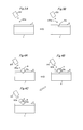
Figs. 3A and 3B are each an illustration showing an opening step of a method for producing the thermoelectric material, in whichFig. 3A shows a state before the formation of a film opening, andFig. 3B shows a state after the formation. -
Figs. 4A to 4C are each an illustration showing a growing step of the method for producing the thermoelectric material, in whichFig. 4A shows a step of creating a nanodot,Fig. 4B shows a step of forming a layer opening in a barrier layer, andFig. 4C shows a step of creating a new nanodot. -
Fig. 5 is an illustration showing a step of creating nanodots made of silicide. -
Fig. 6A is a high-resolution cross-sectional TEM image of epitaxially grown Si nanodots, andFig. 6B is an enlarged view of an area surrounded by the square inFig. 6A . -
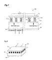
Fig. 7 is a schematic view showing a thermoelectric conversion module according to a second embodiment of the present invention. -
Fig. 8 is a perspective view showing the thermoelectric conversion module according to the second embodiment of the present invention. -
Fig. 9 is a schematic view corresponding toFig. 7 showing an alternative configuration of the thermoelectric conversion module. - A
thermoelectric material 10 according to a first embodiment of the present invention will be described with reference toFigs. 1 and 2 . - As shown in
Figs. 1 and 2 , thethermoelectric material 10 includes asilicon substrate 1, asilicon oxide film 2 formed on thesilicon substrate 1, and athermoelectric layer 3 provided on thesilicon oxide film 2. As thesilicon substrate 1, a single crystal silicon substrate is preferably used. Thesilicon oxide film 2 is preferably an ultrathin oxide film as thick as about a monolayer or bilayer of Si. Thethermoelectric layer 3 has such a configuration that a plurality ofsemiconductor nanodots 4 each surrounded by a potential barrier layer (hereinafter, referred to as the barrier layer) 5 are piled up so as to form a particle packed structure. - The nanodot herein refers to a nanocrystal with a substantially spherical shape or a substantially ellipsoidal shape having a size of a nanometer order. It is to be noted that the nanodot may take a shape which is considerably different from the substantially spherical shape or the substantially ellipsoidal shape depending on a production process. The term "plurality" herein refers to the two or more nanodots being piled up in a vertical direction. For example, when used as a thermoelectric conversion element having an element height of about several tens of µm, the thermoelectric material made of 102 to 105 vertically-piled-up
nanodots 4 may be used. - As shown in the cross-sectional view of
Fig. 2 , thesilicon oxide film 2 has an oxide film opening (hereinafter, referred to as the film opening) 2a formed therein. Thenanodots 4 are provided on and above thefilm opening 2a. Furthermore, thebarrier layer 5 has a barrier layer opening (hereinafter, referred to as the layer opening) 5a formed therein. At least some of the plurality ofnanodots 4 are connected to each other through thelayer openings 5a with their crystal orientation aligned. That is, the plurality ofnanodots 4 are epitaxially grown and piled up on thesilicon oxide film 2. - As described above, the
nanodots 4 are piled up so as to form the particle packed structure. The particle packed structure herein may be a regular packed structure or a random packed structure. Furthermore, some of thenanodots 4 may have the regular packed structure, and others may have the random structure. In order to improve a packing ratio of thenanodots 4 in thethermoelectric layer 3, it is preferable that thenanodots 4 are linearly piled up on thefilm opening 2a. As shown inFig. 2 , however, a plurality oflayer openings 5a may be formed in onebarrier layer 5, and thenanodots 4 may be grown dendritically or randomly. - In addition, while voids are formed among the plurality of
nanodots 4, the void may contain a part made of material such as silicon generated in a process of producing thethermoelectric material 10. - The
nanodots 4 are made of Si, Ge, SiGe, silicide of Mg, silicide of Fe, or silicide of Mn. Chemical formulas of the above silicides are expressed by Mg2Si, β-FeSi2, and MnSix, respectively. In addition, in order to noticeably improve the quantum effect, thenanodots 4 each have a diameter ranging preferably from 1 nm to 100 nm, or more preferably from 2 nm to 50 nm. In order to improve the electric conductivity σ, thenanodots 4 each have an areal density ranging preferably from 109 cm-2 to 1013 cm-2, or more preferably 1011 cm-2 or more. In order to maintain the improved electric conductivity σ, it is preferable that thenanodots 4 are substantially uniform in size. - The
barrier layer 5 is made of material having a bandgap larger than that of the material of thenanodots 4. For example, when thenanodots 4 are made of Si, thebarrier layer 5 may be made of SiO2. When thenanodots 4 are made of Ge, SiGe or silicide, thebarrier layer 5 may be made of Si or SiGe. When thebarrier layer 5 is made of above material other than SiO2, a surface oxide layer (not shown) made of SiO2 is to be formed on an uppermost surface of thebarrier layer 5. In order to sufficiently fulfill the thermoelectric characteristics of the material of thenanodots 4, thebarrier layer 5 preferably has a thickness of 3 nm or less. - With reference to
Figs. 3A and 3B , discussions will be made to a method for producing thethermoelectric material 10 according to the first embodiment of the present invention in a case where thenanodots 4 are made of Si. - The method for producing the
thermoelectric material 10 includes a preparing step S1 of preparing thesilicon substrate 1, an oxidizing step S2 of oxidizing a substrate surface of thesilicon substrate 1 to form thesilicon oxide film 2, an opening step S3 of forming thefilm openings 2a in thesilicon oxide film 2, and a growing step S4 of epitaxially growing to pile up thenanodots 4 made of Si on thefilm openings 2a. - In the oxidizing step S2, the surface of the
silicon substrate 1 is oxidized under a condition of low oxygen partial pressure and high temperature such as an oxygen partial pressure of 2 x 10⁻⁴ Pa and a temperature of 600°C, whereby thesilicon oxide film 2 as thick as a monolayer or bilayer is formed. - Then, in the opening step S3, the
silicon oxide film 2 is irradiated with a molecular beam ofSi 20a generated by asilicon evaporation source 20 shown inFig. 3A under a condition of high vacuum (such as 10-5 Pa or less) and about 500°C or more. Thus, thesilicon oxide film 2 disappears and SiO sublimes to form thefilm opening 2a as shown inFig. 3B through a reaction shown in the following formula (1).
Si + SiO2 → 2SiO ↑ ... (1)
- Then, in the growing step S4, as shown in
Fig. 4A , thesilicon oxide film 2 is irradiated with the molecular beam ofSi 20a. Then, Si atoms are deposited to a Si dangling bond in the surface of thesilicon substrate 1 which has been exposed after the formation of thefilm opening 2a, whereby thenanodots 4 are created. - Then, the irradiation of the molecular beam of
Si 20a is stopped, and thenanodots 4 made of Si are oxidized, whereby thebarrier layer 5 made of SiO2 is provided around each of thenanodots 4. Then, as shown inFig. 4B , similarly to the formation of thefilm opening 2a, the irradiation of the molecular beam ofSi 20a is started again to form thelayer opening 5a according to the above formula (1). At this step, thelayer opening 5a may be formed in the same vacuum condition and temperature condition as those of the opening step S3 of forming thefilm opening 2a, or may be formed under different vacuum condition and temperature condition in view of the size and/or composition of thebarrier layer 5, for example. - Finally, as shown in
Fig. 4C , the Si atoms are deposited on thelayer opening 5a, whereby anew nanodot 4 is created. At this time, many of thenanodots 4 are connected to each other through thelayer openings 5a with their crystal orientation aligned. That is, by repeating the processes shown inFigs. 4A to 4C , the plurality ofnanodots 4 are epitaxially grown and piled up on and above thefilm openings 2a formed in thesilicon oxide film 2. - The opening step S3 and the growing step S4 have been separately described. When the
nanodots 4 are created with Si, however, the formation of thefilm opening 2a in the opening step S3, and the creation of thenanodots 4 in the growing step S4 are to be continuously performed by irradiating thesilicon oxide film 2 with the molecular beam ofSi 20a. - The
film opening 2a is formed by the irradiation of the molecular beam ofSi 20a in this embodiment, but it may be formed by irradiation of a molecular beam of Ge generated by a germanium evaporation source (not shown). In the latter case, thesilicon oxide film 2 disappears and SiO and GeO sublime to form the film opening 2a through a reaction shown in the following formula (2).
Ge + SiO2 → SiO T + GeO ↑ ... (2)
- Discussions have been made to the case where the
nanodots 4 are made of Si in this embodiment. When thenanodots 4 are made of SiGe, silicide, etc., the opening step S3 and the growing step S4 are performed with a plurality of evaporation sources. For example, when thenanodots 4 are made of iron silicide, thefilm opening 2a is formed with the molecular beam ofSi 20a generated by thesilicon evaporation source 20, as shown inFig. 5 . Then, thenanodots 4 made of iron silicide can be created by irradiation of the molecular beam ofSi 20a and a molecular beam ofFe 22a generated by aniron evaporation source 22, at an atmospheric temperature of 250°C to 600°C, for example. The nanodots made of manganese silicide or magnesium silicide can be created under the same condition. - Furthermore, after the creation of the
nanodots 4, thebarrier layer 5 made of desired material can be provided by irradiation of the molecular beam of the material such as Si, SiGe, silicide or the like. Thus, when thebarrier layer 5 is made of material other than SiO2, thebarrier layer 5 is oxidized to form a surface oxide layer made of SiO2 on its surface, and then as described above, the molecular beam ofSi 20a (molecular beam of Ge) is applied, whereby thelayer opening 5a is formed according to the above formula (1) or (2). -
Fig. 6A is a high-resolution cross-sectional TEM image of the thermoelectric layer part of the thermoelectric material produced by the above method, which shows a cross-sectional surface of the Si nanodots epitaxially grown on the single crystal silicon substrate. The nanodots were created so as to form a diameter of about 3 nm. The barrier layer made of SiO2 is as thick as the monolayer or bilayer, that is, its thickness is less than 1 nm, so that it is not visible inFig. 6A . Meanwhile, as shown inFig. 6B which is an enlarged view of an area surrounded by the square inFig. 6A , it is found that substantially sphere-shaped nanodots made of Si are created in the circled areas. Furthermore, it is found that voids are generated among the circled areas, and the nanodots are spread randomly and piled up. - The thermal conductivity k of the thermoelectric material produced as described above was measured by the 2ω method. In the 2ω method, a voltage having a frequency ω is applied to the thermoelectric material, generated Joule heat changes at a frequency of 2ω, and therefore, an electric resistance value of the thermoelectric material also changes at the frequency of 2ω. According to this principle, amplitude of an output voltage was measured to obtain the thermal conductivity k.
- As a result, the thermal conductivity k showed a very small value such as k = 0.67 ± 0.11 W/mK. When comparing this value with the thermal conductivity k of bulk Si of about 150 W/mK, it is found that the value of thermal conductivity k of the thermoelectric layer, which is made of the nanodots piled up as in the case of this embodiment, is considerably reduced. Furthermore, it is generally known that when the material is to be made amorphous, phonon scattering is increased, and the value of the thermal conductivity k is minimized. The value of the thermal conductivity k of the thermoelectric material produced by the production method according to this embodiment is considerably smaller than the thermal conductivity of 2.0 W/mK of amorphous silicon.
- In this embodiment, the
thermoelectric material 10 including thethermoelectric layer 3 having the plurality ofnanodots 4, and the method for producing the same have been described. According to this embodiment wherethermoelectric layer 3 includes the plurality ofnanodots 4, the increase of the phonon scattering due to the nanostructure reduces the thermal conductivity k. Especially, when thenanodots 4 are made of Si, the problematic thermal conductivity k can be considerably reduced as can be seen from the result of the 2ω method. - In addition, at least some of the
nanodots 4 are connected with their crystal orientation aligned, thereby improving the electric conductivity σ. The quantum effect can be obtained due to the nanostructure, thereby increasing the power factor S2σ. As a result, the performance index ZT is considerably increased, and thus thethermoelectric material 10 which is superior in thermoelectric performance can be provided. - According to the semiconductor device disclosed in
Patent document 1, a spacer layer is provided and thus a proportion of the material of the spacer layer to the material of the nanodots is high (refer to Fig. 10). Therefore, the thermoelectric characteristics of the material of the nanodots are not sufficiently fulfilled. Meanwhile, this embodiment in which thenanodots 4 are piled up, and in which thebarrier layer 5 is provided around each of thenanodots 4, leads to the high proportion of the material of thenanodots 4, and the superior thermoelectric characteristics of the material can be implemented due to the nanostructure. - In addition, the
nanodots 4 are each provided on thefilm opening 2a formed in thesilicon oxide film 2, which results in thenanodots 4 epitaxially growing across the amorphous structure of SiO2 which increases the phonon scattering. - Furthermore, the
nanodots 4 each have thebarrier layer 5 having the thickness of 10 nm or less, that is, as thick as several atomic layers around its periphery, and are connected toother nanodots 4 through thelayer opening 5a formed in thebarrier layer 5. This structure can be created by continuous irradiation of the molecular beam, thereby simplifying the production process of thethermoelectric material 10. - In the above, the case where the
film opening 2a is formed in thesilicon oxide film 2 on thesilicon substrate 1 has been described, but even when a semiconductor oxide film is formed on a semiconductor substrate other than the silicon substrate, the thermoelectric material having the same structure as thethermoelectric material 10 in this embodiment can be obtained by forming an opening in this oxide film. The semiconductor oxide film may be a SixGeyOz film formed by oxidizing a SiGe mixed crystal substrate, a GeOx film formed by oxidizing a Ge substrate, and the like. When the molecular beam of Si is used, the opening is formed through reactions expressed by the following formulas (3) and (4).
SixGeyOz + aSi → bSiO T + cGeO ↑ ... (3)
GeOx + dSi → eSiO T + GeO T ... (4)
When a molecular beam of Ge is used, the opening is formed through reactions expressed by the following formulas (5) and (6).
SixGeyOz + fGe → gSiO ↑ + hGeO ↑ ... (5)
GeOx + iGe → jGeO ↑ ... (6)
The factors a to j are determined by x, y and z. The opening can also be formed in an oxide film formed by oxidizing a silicide expressed by the chemical formula of SiFexOy. - Furthermore, the case where the substrate made of semiconductor is used as the substrate of the
thermoelectric material 10 has been described, but the semiconductor substrate may be provided such that a semiconductor thin film is deposited on a glass substrate by electron beam heating or the like. Alternatively, another semiconductor thin film may be formed on the silicon substrate or the like. - A
thermoelectric material 60 according to a second embodiment of the present invention will be described with reference toFig. 1 , etc. used in the description of the first embodiment. - In the growing step S4 of the method for producing the thermoelectric material according to the first embodiment, the irradiation is executed with the molecular beam of the material such as Si, Ge, SiGe, or silicide of the nanodots 4 (refer to
Figs. 4A to 4C ). Meanwhile, in the growing step S4 according to this embodiment, irradiation is executed with a molecular beam of a dopant, that is, a donor atom or acceptor atom, in addition to the molecular beam of the material ofnanodots 54. As a result, thenanodots 54 of thethermoelectric layer 53 are doped, and thethermoelectric material 60 serves as a p-type semiconductor or an n-type semiconductor. Other than the above, a configuration of thethermoelectric material 60 and steps of a method for producing thethermoelectric material 60 are the same as those of the first embodiment, and the same reference symbol is given thereto and their description is omitted. - When the
nanodots 54 are made of Si or Ge, the acceptor atom may include boron, aluminum, gallium and indium, while the donor atom may include phosphor, arsenic and antimony, for example. When thenanodots 54 are made of the material other than Si and Ge, the acceptor atom or the donor atom may include the well-known material for the person skilled in the art. -
Fig. 7 is a schematic view showing athermoelectric conversion module 70 according to the second embodiment of the present invention. Thethermoelectric conversion module 70 includes a thermoelectric conversion element using thethermoelectric material 60. The thermoelectric conversion module herein refers to an assembly of the plurality of thermoelectric conversion elements. - As shown in
Fig. 7 , thethermoelectric conversion module 70 has the thermoelectric conversion elements, that is, p-typethermoelectric elements 71a and n-typethermoelectric elements 71b alternately arranged betweenelectrodes electrode 72a is provided on a module face of asilicon substrate 81, and theelectrode 72b has an electric insulatingmaterial 73 such as a ceramic plate provided thereon. - In
Fig. 7 , thethermoelectric conversion module 70 appears to be arranged in a two-dimensional manner for convenience, but thethermoelectric conversion module 70 is actually arranged in a three-dimensional manner as shown inFig. 8 . InFig. 8 , theelectrodes - The face opposite to the module face, on which the
thermoelectric conversion module 70 is provided, has asilicon oxide film 82 formed thereon. Thesilicon oxide film 82 has asemiconductor device 83 such as MOSFET (refer toFig. 7 ) provided thereon. - The
thermoelectric conversion module 70 thermoelectrically converts joule heat generated by an operation of thesemiconductor device 83 and transmitted to the module face of thesilicon substrate 81. - As shown in
Fig. 7 , the p-type and n-typethermoelectric elements thermoelectric material 60 created through the doping as described above can be used as the p-type and n-typethermoelectric elements - The
electrode 72a can be provided such that a metal such as aluminum is deposited on thesemiconductor substrate 81, and then subjected to a photolithography step. In general, since the deposition of the metal and the photolithography step are included in forming thesemiconductor device 83, theelectrode 72a can be provided at the same time as the formation of thedevice 83. The p-type and n-typethermoelectric elements electrodes thermoelectric conversion module 70 is provided on the module face of thesilicon substrate 81. Furthermore, bonding members may be interposed between the p-type and n-typethermoelectric elements electrodes - Meanwhile,
Fig. 9 shows an alternative configuration of thethermoelectric conversion module 70 according to this embodiment. According to this configuration, aconductive layer 74 is formed on an upper face of thesilicon substrate 81 by highly doping an impurity such as aluminum by thermal diffusion, and then, theelectrode 72a is formed through an etching step as shown inFig. 9 . Then, a silicon oxide film (not shown) is formed on theelectrode 72a by oxidizing theelectrode 72a, which is followed by the above-described opening step S3 and the growing step S4. Thus, thethermoelectric material 60, of which the p-type and n-typethermoelectric elements electrode 72a are made, is provided on thesilicon substrate 81. - As described above, according to this embodiment, the
nanodots 54 of thethermoelectric material 60 have the acceptor atom or the donor atom, so that thethermoelectric material 60 can be used as the p-type and n-typethermoelectric elements thermoelectric conversion module 70. - When the
thermoelectric conversion module 70 is provided on a reverse surface of thesemiconductor device 83 such as an LSI, exhaust heat generated from thesemiconductor device 83 is converted to electric energy by thethermoelectric conversion module 70. This leads to the advantage that it is not necessary to consume power to cool down thesemiconductor device 83 to prevent the temperature from rising due to the exhaust heat, and further the exhaust heat can be effectively used, so that energy efficiency can be considerably enhanced in an entire system. - Furthermore, according to the alternative configuration shown in
Fig. 9 , the step of bonding the p-type and n-typethermoelectric elements thermoelectric module 70 can be completely combined in the formation of thesemiconductor device 83, so that thethermoelectric module 70 can be easily and efficiently provided. - Discussions have been made to the case where the p-type and n-type semiconductors of the
thermoelectric material 60 produced in this embodiment are used as the thermoelectric power-generating module, but they can be used as a Peltier module based on similar configurations. - For example, two
thermoelectric modules 70 according to this embodiment can be laminated on the reverse surface (module face) of the LSI, the first module (closer to the LSI) as the Peltier module, while the second module as the thermoelectric power-generating module. When the Peltier module is operated, the LSI side of this module is cooled down and its opposite side is heated to high temperature. This heat is transferred to the thermoelectric power-generating module to generate power. Similarly to other instances, this enables the improvement of the energy efficiency of an entire system with the effective use of exhaust heat. - In addition, when the
thermoelectric material silicon substrate 1 provided by crystalizing a surface of a polycrystalline silicon substrate, for example, thethermoelectric material - The thermoelectric material according to the present invention can be widely used in producing a thermoelectric conversion element for mutually converting thermal energy and electric energy, a light emitting element such as a laser, and a solar battery.
-
- 1
- silicon substrate
- 2
- silicon oxide film
- 2a
- oxide film opening (first nano-opening)
- 3
- thermoelectric layer
- 4
- nanodot(s)
- 5
- barrier layer
- 5a
- barrier layer opening (second nano-opening)
- 10, 60
- thermoelectric material
- 20
- silicon evaporation source
- 22
- iron evaporation source
- 70
- thermoelectric conversion module
- 83
- semiconductor device
Claims (12)
- A thermoelectric material comprising:a semiconductor substrate;a semiconductor oxide film formed on the semiconductor substrate; anda thermoelectric layer provided on the semiconductor oxide film; whereinthe semiconductor oxide film has a first nano-opening formed therein,the thermoelectric layer has such a configuration that a plurality of semiconductor nanodots are piled up on or above the first nano-opening so as to form a particle packed structure, andat least some of the plurality of semiconductor nanodots each have a second nano-opening formed in its surface, and are connected to each other through the second nano-opening with their crystal orientation aligned.
- The thermoelectric material according to claim 1, wherein each of the semiconductor nanodots has a potential barrier layer provided on its surface, and
the second nano-opening is formed in the potential barrier layer. - The thermoelectric material according to claim 1 or 2, wherein each of the semiconductor nanodots is made of material selected from the group consisting of Si, Ge, SiGe, silicon based compound of Mg, silicon based compound of Fe, and silicon based compound of Mn.
- The thermoelectric material according to claim 2, wherein the potential barrier layer is made of SiO2.
- The thermoelectric material according to claim 2, wherein the potential barrier layer is made of Si, and has an oxide layer made of SiO2 on its surface.
- The thermoelectric material according to any one of claims 1 to 5, wherein each of the semiconductor nanodots has a diameter ranging from 2 nm to 50 nm.
- The thermoelectric material according to any one of claims 1 to 6, wherein each of the semiconductor nanodots has an areal density of 1011 cm-2 or more.
- The thermoelectric material according to claim 2, wherein the potential barrier layer has a thickness of 3 nm or less.
- The thermoelectric material according to any one of claims 1 to 8, wherein each of the semiconductor nanodots contains a p-type or n-type dopant.
- A thermoelectric conversion module provided with p-type and n-type thermoelectric elements alternately arranged and electrically connected in series, wherein
the p-type and n-type thermoelectric elements each comprise the thermoelectric material according to claim 9, and are provided on a principal surface opposite to a principal surface of the semiconductor substrate having a semiconductor device. - A method for producing a thermoelectric material comprising:a step of preparing a semiconductor substrate;a step of oxidizing the semiconductor substrate to form a semiconductor oxide film on the semiconductor substrate;a step of forming a first nano-opening in the semiconductor oxide film; anda step of epitaxially growing to pile up a plurality of semiconductor nanodots made of semiconductor material on the first nano-opening.
- The method for producing a thermoelectric material according to claim 11, wherein in the step of epitaxially growing, a second nano-opening is formed in each of the semiconductor nanodots, and the nanodots are connected to each other through the second nano-opening.
Applications Claiming Priority (2)
| Application Number | Priority Date | Filing Date | Title |
|---|---|---|---|
| JP2012124940 | 2012-05-31 | ||
| PCT/JP2013/063580 WO2013179897A1 (en) | 2012-05-31 | 2013-05-15 | Thermoelectric material, method for producing same, and thermoelectric conversion module using same |
Publications (3)
| Publication Number | Publication Date |
|---|---|
| EP2784835A1 true EP2784835A1 (en) | 2014-10-01 |
| EP2784835A4 EP2784835A4 (en) | 2014-12-10 |
| EP2784835B1 EP2784835B1 (en) | 2016-03-16 |
Family
ID=49673100
Family Applications (1)
| Application Number | Title | Priority Date | Filing Date |
|---|---|---|---|
| EP13796323.7A Active EP2784835B1 (en) | 2012-05-31 | 2013-05-15 | Thermoelectric material, method for producing same, and thermoelectric conversion module using same |
Country Status (8)
| Country | Link |
|---|---|
| US (1) | US9076925B2 (en) |
| EP (1) | EP2784835B1 (en) |
| JP (1) | JP5424436B1 (en) |
| KR (1) | KR101482598B1 (en) |
| CN (1) | CN103959496B (en) |
| RU (1) | RU2561659C1 (en) |
| TW (1) | TWI462354B (en) |
| WO (1) | WO2013179897A1 (en) |
Cited By (2)
| Publication number | Priority date | Publication date | Assignee | Title |
|---|---|---|---|---|
| JP2017107932A (en) * | 2015-12-08 | 2017-06-15 | 富士通株式会社 | Thermoelectric conversion element and manufacturing method thereof |
| CN109314172A (en) * | 2016-03-22 | 2019-02-05 | 金瑟姆股份有限公司 | Distributed thermoelectric materials with non-uniform heat transfer properties |
Families Citing this family (12)
| Publication number | Priority date | Publication date | Assignee | Title |
|---|---|---|---|---|
| JP6411782B2 (en) * | 2013-08-07 | 2018-10-24 | 株式会社Nttファシリティーズ | Method for manufacturing thermoelectric material |
| WO2016002061A1 (en) * | 2014-07-04 | 2016-01-07 | 株式会社日立製作所 | Thermoelectric conversion material, thermoelectric conversion element, thermoelectric conversion module, and method for manufacturing thermoelectric conversion material |
| TWI560916B (en) * | 2014-07-31 | 2016-12-01 | Univ Nat Tsing Hua | Manufacturing process of the thermoelectric conversion element |
| WO2017002514A1 (en) * | 2015-06-30 | 2017-01-05 | 住友電気工業株式会社 | Thermoelectric material, thermoelectric element, optical sensor, and method for producing thermoelectric material |
| RU2654305C1 (en) * | 2016-12-06 | 2018-05-17 | ООО "НПО "Синергетика" | Thermoelectric device for spot cooling |
| KR101948638B1 (en) * | 2017-03-15 | 2019-02-15 | 고려대학교 산학협력단 | An oxide-based resistive switching memory device using a single nano-pore structure and method for fabricating the device |
| WO2018225388A1 (en) * | 2017-06-08 | 2018-12-13 | 住友電気工業株式会社 | Thermoelectric conversion material, thermoelectric conversion element and production method of thermoelectric conversion material |
| JP7010474B2 (en) * | 2018-01-10 | 2022-02-10 | 国立研究開発法人物質・材料研究機構 | Insulation material, its manufacturing method and internal combustion engine |
| US11402672B2 (en) * | 2018-05-03 | 2022-08-02 | X Development Llc | Quantum confined nanostructures with improved homogeneity and methods for making the same |
| CN110729392B (en) * | 2019-10-23 | 2023-09-29 | 华北电力大学(保定) | A layered silicon germanium thermoelectric material |
| CN113130731A (en) * | 2019-12-30 | 2021-07-16 | 华为技术有限公司 | Thermoelectric refrigerator, method for manufacturing thermoelectric refrigerator, and electronic apparatus |
| JP7493775B2 (en) * | 2020-08-31 | 2024-06-03 | 国立大学法人東北大学 | Porous film made of intermetallic compound, and its manufacturing method and application |
Family Cites Families (22)
| Publication number | Priority date | Publication date | Assignee | Title |
|---|---|---|---|---|
| JPH05343746A (en) * | 1992-06-09 | 1993-12-24 | Matsushita Electric Ind Co Ltd | Thermoelectric material and manufacture thereof |
| US5866039A (en) * | 1995-01-13 | 1999-02-02 | The United States Of America As Represented By The Secretary Of The Army | Luminescent device for displays and lighting |
| JPH10209508A (en) | 1997-01-22 | 1998-08-07 | Toshiba Corp | Thermoelectric conversion element and method for manufacturing the same |
| JP3559962B2 (en) | 2000-09-04 | 2004-09-02 | 日本航空電子工業株式会社 | Thermoelectric conversion material and method for producing the same |
| JP2004228273A (en) | 2003-01-22 | 2004-08-12 | Renesas Technology Corp | Semiconductor device |
| JP4508761B2 (en) | 2004-03-18 | 2010-07-21 | 独立行政法人科学技術振興機構 | Manufacturing method of semiconductor device |
| US7309830B2 (en) * | 2005-05-03 | 2007-12-18 | Toyota Motor Engineering & Manufacturing North America, Inc. | Nanostructured bulk thermoelectric material |
| JP2006190773A (en) | 2005-01-05 | 2006-07-20 | Matsushita Electric Ind Co Ltd | Micro semiconductor structure and manufacturing method thereof |
| US20060207647A1 (en) * | 2005-03-16 | 2006-09-21 | General Electric Company | High efficiency inorganic nanorod-enhanced photovoltaic devices |
| JP4830383B2 (en) * | 2005-07-19 | 2011-12-07 | 大日本印刷株式会社 | Core-shell type nanoparticles and thermoelectric conversion materials |
| JP5173433B2 (en) | 2005-12-07 | 2013-04-03 | トヨタ自動車株式会社 | Thermoelectric conversion material and manufacturing method thereof |
| DE102005063038A1 (en) | 2005-12-29 | 2007-07-05 | Basf Ag | Nano wires or nano tubes manufacturing method for e.g. air conditioning system, involves providing melted mass or solution, which contains thermo electric active material or precursor compounds of thermo electric active materials |
| US20080073743A1 (en) * | 2006-02-17 | 2008-03-27 | Lockheed Martin Corporation | Templated growth of semiconductor nanostructures, related devices and methods |
| US8044292B2 (en) * | 2006-10-13 | 2011-10-25 | Toyota Motor Engineering & Manufacturing North America, Inc. | Homogeneous thermoelectric nanocomposite using core-shell nanoparticles |
| US8426722B2 (en) * | 2006-10-24 | 2013-04-23 | Zetta Research and Development LLC—AQT Series | Semiconductor grain and oxide layer for photovoltaic cells |
| WO2008140596A2 (en) | 2006-12-01 | 2008-11-20 | Massachusetts Institute Of Technology (Mit) | Methods for high figure-of-merit in nanostructured thermoelectric materials |
| RU2376681C1 (en) | 2008-10-06 | 2009-12-20 | Учреждение Российской академии наук Физико-технический институт им. А.Ф. Иоффе РАН | Thermoelectric cell |
| KR100996675B1 (en) | 2009-01-14 | 2010-11-25 | 연세대학교 산학협력단 | Thermoelectric Nanowires and Manufacturing Method Thereof |
| KR101538068B1 (en) * | 2009-02-02 | 2015-07-21 | 삼성전자주식회사 | Thermoelectric element and its manufacturing method |
| RU91476U1 (en) | 2009-11-19 | 2010-02-10 | Государственное учреждение "Научно-исследовательский институт микроэлектроники и информационно-измерительной техники Московского государственного института электроники и математики (технического университета)" | THERMOELECTRIC CONVERTER BASED ON EPITAXIAL STRUCTURE |
| JP2011134745A (en) * | 2009-12-22 | 2011-07-07 | Sumitomo Metal Mining Co Ltd | Thermoelectric powder, thermoelectric conversion element employing the same, and thermoelectric conversion module |
| JP2011159871A (en) * | 2010-02-02 | 2011-08-18 | Toyota Motor Corp | Method of forming nanocomposite thermoelectric material thin film |
-
2013
- 2013-05-15 EP EP13796323.7A patent/EP2784835B1/en active Active
- 2013-05-15 RU RU2014118878/28A patent/RU2561659C1/en active
- 2013-05-15 US US14/355,598 patent/US9076925B2/en active Active
- 2013-05-15 JP JP2013543430A patent/JP5424436B1/en active Active
- 2013-05-15 KR KR1020147013536A patent/KR101482598B1/en active Active
- 2013-05-15 CN CN201380003966.4A patent/CN103959496B/en active Active
- 2013-05-15 WO PCT/JP2013/063580 patent/WO2013179897A1/en not_active Ceased
- 2013-05-29 TW TW102118876A patent/TWI462354B/en active
Cited By (2)
| Publication number | Priority date | Publication date | Assignee | Title |
|---|---|---|---|---|
| JP2017107932A (en) * | 2015-12-08 | 2017-06-15 | 富士通株式会社 | Thermoelectric conversion element and manufacturing method thereof |
| CN109314172A (en) * | 2016-03-22 | 2019-02-05 | 金瑟姆股份有限公司 | Distributed thermoelectric materials with non-uniform heat transfer properties |
Also Published As
| Publication number | Publication date |
|---|---|
| KR20140070672A (en) | 2014-06-10 |
| US20140299172A1 (en) | 2014-10-09 |
| EP2784835B1 (en) | 2016-03-16 |
| WO2013179897A1 (en) | 2013-12-05 |
| TWI462354B (en) | 2014-11-21 |
| JPWO2013179897A1 (en) | 2016-01-18 |
| EP2784835A4 (en) | 2014-12-10 |
| TW201405896A (en) | 2014-02-01 |
| RU2561659C1 (en) | 2015-08-27 |
| CN103959496A (en) | 2014-07-30 |
| KR101482598B1 (en) | 2015-01-14 |
| US9076925B2 (en) | 2015-07-07 |
| CN103959496B (en) | 2015-05-13 |
| JP5424436B1 (en) | 2014-02-26 |
Similar Documents
| Publication | Publication Date | Title |
|---|---|---|
| EP2784835B1 (en) | Thermoelectric material, method for producing same, and thermoelectric conversion module using same | |
| US9209375B2 (en) | Methods and devices for controlling thermal conductivity and thermoelectric power of semiconductor nanowires | |
| Nielsch et al. | Thermoelectric nanostructures: from physical model systems towards nanograined composites | |
| US8536440B2 (en) | Semiconductor nanowire thermoelectric materials and devices, and processes for producing same | |
| US8729381B2 (en) | Nanostructures having high performance thermoelectric properties | |
| EP2329055B1 (en) | Sige matrix nanocomposite materials with an improved thermoelectric figure of merit | |
| JP5282598B2 (en) | Method for manufacturing thermoelectric conversion element | |
| Ali et al. | Nanowire-based thermoelectrics | |
| US10944037B2 (en) | Thermoelectric material, thermoelectric element, optical sensor, and method for manufacturing thermoelectric material | |
| CN103682073B (en) | Thermoelement | |
| JP6609109B2 (en) | Thermoelectric conversion element and method for manufacturing the same, thermoelectric power generation device and Peltier device | |
| KR102097063B1 (en) | Thermoelectric material, thermoelectric device and apparatus comprising same, and preparation method thereof | |
| US20140373891A1 (en) | Thermoelectric structure, and thermoelectric device and thermoelectric apparatus including the same | |
| CN109219894B (en) | Thermoelectric material, thermoelectric element, optical sensor, and method for producing thermoelectric material | |
| Dresselhaus et al. | Advances in 1D and 2D thermoelectric materials | |
| KR20110071291A (en) | Thermoelectric element using superlattice | |
| JP2017107932A (en) | Thermoelectric conversion element and manufacturing method thereof | |
| Zhou et al. | Nanocomposite materials for thermoelectric energy conversion: A brief survey of recent patents | |
| Nassiopoulou | Porous Silicon as a Material for Thermoelectric Devices |
Legal Events
| Date | Code | Title | Description |
|---|---|---|---|
| PUAI | Public reference made under article 153(3) epc to a published international application that has entered the european phase |
Free format text: ORIGINAL CODE: 0009012 |
|
| 17P | Request for examination filed |
Effective date: 20140627 |
|
| AK | Designated contracting states |
Kind code of ref document: A1 Designated state(s): AL AT BE BG CH CY CZ DE DK EE ES FI FR GB GR HR HU IE IS IT LI LT LU LV MC MK MT NL NO PL PT RO RS SE SI SK SM TR |
|
| A4 | Supplementary search report drawn up and despatched |
Effective date: 20141110 |
|
| RIC1 | Information provided on ipc code assigned before grant |
Ipc: H01L 35/34 20060101ALI20141104BHEP Ipc: H01L 35/14 20060101ALI20141104BHEP Ipc: H01L 35/32 20060101AFI20141104BHEP |
|
| DAX | Request for extension of the european patent (deleted) | ||
| GRAP | Despatch of communication of intention to grant a patent |
Free format text: ORIGINAL CODE: EPIDOSNIGR1 |
|
| INTG | Intention to grant announced |
Effective date: 20151023 |
|
| GRAS | Grant fee paid |
Free format text: ORIGINAL CODE: EPIDOSNIGR3 |
|
| GRAA | (expected) grant |
Free format text: ORIGINAL CODE: 0009210 |
|
| AK | Designated contracting states |
Kind code of ref document: B1 Designated state(s): AL AT BE BG CH CY CZ DE DK EE ES FI FR GB GR HR HU IE IS IT LI LT LU LV MC MK MT NL NO PL PT RO RS SE SI SK SM TR |
|
| REG | Reference to a national code |
Ref country code: GB Ref legal event code: FG4D |
|
| REG | Reference to a national code |
Ref country code: CH Ref legal event code: EP |
|
| REG | Reference to a national code |
Ref country code: IE Ref legal event code: FG4D |
|
| REG | Reference to a national code |
Ref country code: AT Ref legal event code: REF Ref document number: 781903 Country of ref document: AT Kind code of ref document: T Effective date: 20160415 |
|
| REG | Reference to a national code |
Ref country code: FR Ref legal event code: PLFP Year of fee payment: 4 |
|
| REG | Reference to a national code |
Ref country code: DE Ref legal event code: R096 Ref document number: 602013005597 Country of ref document: DE |
|
| REG | Reference to a national code |
Ref country code: NL Ref legal event code: MP Effective date: 20160316 |
|
| REG | Reference to a national code |
Ref country code: LT Ref legal event code: MG4D |
|
| PG25 | Lapsed in a contracting state [announced via postgrant information from national office to epo] |
Ref country code: NO Free format text: LAPSE BECAUSE OF FAILURE TO SUBMIT A TRANSLATION OF THE DESCRIPTION OR TO PAY THE FEE WITHIN THE PRESCRIBED TIME-LIMIT Effective date: 20160616 Ref country code: HR Free format text: LAPSE BECAUSE OF FAILURE TO SUBMIT A TRANSLATION OF THE DESCRIPTION OR TO PAY THE FEE WITHIN THE PRESCRIBED TIME-LIMIT Effective date: 20160316 Ref country code: FI Free format text: LAPSE BECAUSE OF FAILURE TO SUBMIT A TRANSLATION OF THE DESCRIPTION OR TO PAY THE FEE WITHIN THE PRESCRIBED TIME-LIMIT Effective date: 20160316 Ref country code: GR Free format text: LAPSE BECAUSE OF FAILURE TO SUBMIT A TRANSLATION OF THE DESCRIPTION OR TO PAY THE FEE WITHIN THE PRESCRIBED TIME-LIMIT Effective date: 20160617 |
|
| REG | Reference to a national code |
Ref country code: AT Ref legal event code: MK05 Ref document number: 781903 Country of ref document: AT Kind code of ref document: T Effective date: 20160316 |
|
| PG25 | Lapsed in a contracting state [announced via postgrant information from national office to epo] |
Ref country code: SE Free format text: LAPSE BECAUSE OF FAILURE TO SUBMIT A TRANSLATION OF THE DESCRIPTION OR TO PAY THE FEE WITHIN THE PRESCRIBED TIME-LIMIT Effective date: 20160316 Ref country code: LT Free format text: LAPSE BECAUSE OF FAILURE TO SUBMIT A TRANSLATION OF THE DESCRIPTION OR TO PAY THE FEE WITHIN THE PRESCRIBED TIME-LIMIT Effective date: 20160316 Ref country code: RS Free format text: LAPSE BECAUSE OF FAILURE TO SUBMIT A TRANSLATION OF THE DESCRIPTION OR TO PAY THE FEE WITHIN THE PRESCRIBED TIME-LIMIT Effective date: 20160316 Ref country code: NL Free format text: LAPSE BECAUSE OF FAILURE TO SUBMIT A TRANSLATION OF THE DESCRIPTION OR TO PAY THE FEE WITHIN THE PRESCRIBED TIME-LIMIT Effective date: 20160316 Ref country code: BE Free format text: LAPSE BECAUSE OF NON-PAYMENT OF DUE FEES Effective date: 20160531 Ref country code: LV Free format text: LAPSE BECAUSE OF FAILURE TO SUBMIT A TRANSLATION OF THE DESCRIPTION OR TO PAY THE FEE WITHIN THE PRESCRIBED TIME-LIMIT Effective date: 20160316 |
|
| PG25 | Lapsed in a contracting state [announced via postgrant information from national office to epo] |
Ref country code: EE Free format text: LAPSE BECAUSE OF FAILURE TO SUBMIT A TRANSLATION OF THE DESCRIPTION OR TO PAY THE FEE WITHIN THE PRESCRIBED TIME-LIMIT Effective date: 20160316 Ref country code: IS Free format text: LAPSE BECAUSE OF FAILURE TO SUBMIT A TRANSLATION OF THE DESCRIPTION OR TO PAY THE FEE WITHIN THE PRESCRIBED TIME-LIMIT Effective date: 20160716 Ref country code: PL Free format text: LAPSE BECAUSE OF FAILURE TO SUBMIT A TRANSLATION OF THE DESCRIPTION OR TO PAY THE FEE WITHIN THE PRESCRIBED TIME-LIMIT Effective date: 20160316 |
|
| PG25 | Lapsed in a contracting state [announced via postgrant information from national office to epo] |
Ref country code: ES Free format text: LAPSE BECAUSE OF FAILURE TO SUBMIT A TRANSLATION OF THE DESCRIPTION OR TO PAY THE FEE WITHIN THE PRESCRIBED TIME-LIMIT Effective date: 20160316 Ref country code: CZ Free format text: LAPSE BECAUSE OF FAILURE TO SUBMIT A TRANSLATION OF THE DESCRIPTION OR TO PAY THE FEE WITHIN THE PRESCRIBED TIME-LIMIT Effective date: 20160316 Ref country code: SK Free format text: LAPSE BECAUSE OF FAILURE TO SUBMIT A TRANSLATION OF THE DESCRIPTION OR TO PAY THE FEE WITHIN THE PRESCRIBED TIME-LIMIT Effective date: 20160316 Ref country code: PT Free format text: LAPSE BECAUSE OF FAILURE TO SUBMIT A TRANSLATION OF THE DESCRIPTION OR TO PAY THE FEE WITHIN THE PRESCRIBED TIME-LIMIT Effective date: 20160718 Ref country code: RO Free format text: LAPSE BECAUSE OF FAILURE TO SUBMIT A TRANSLATION OF THE DESCRIPTION OR TO PAY THE FEE WITHIN THE PRESCRIBED TIME-LIMIT Effective date: 20160316 Ref country code: SM Free format text: LAPSE BECAUSE OF FAILURE TO SUBMIT A TRANSLATION OF THE DESCRIPTION OR TO PAY THE FEE WITHIN THE PRESCRIBED TIME-LIMIT Effective date: 20160316 Ref country code: AT Free format text: LAPSE BECAUSE OF FAILURE TO SUBMIT A TRANSLATION OF THE DESCRIPTION OR TO PAY THE FEE WITHIN THE PRESCRIBED TIME-LIMIT Effective date: 20160316 |
|
| REG | Reference to a national code |
Ref country code: DE Ref legal event code: R097 Ref document number: 602013005597 Country of ref document: DE |
|
| PG25 | Lapsed in a contracting state [announced via postgrant information from national office to epo] |
Ref country code: BE Free format text: LAPSE BECAUSE OF FAILURE TO SUBMIT A TRANSLATION OF THE DESCRIPTION OR TO PAY THE FEE WITHIN THE PRESCRIBED TIME-LIMIT Effective date: 20160316 Ref country code: LU Free format text: LAPSE BECAUSE OF FAILURE TO SUBMIT A TRANSLATION OF THE DESCRIPTION OR TO PAY THE FEE WITHIN THE PRESCRIBED TIME-LIMIT Effective date: 20160515 Ref country code: IT Free format text: LAPSE BECAUSE OF FAILURE TO SUBMIT A TRANSLATION OF THE DESCRIPTION OR TO PAY THE FEE WITHIN THE PRESCRIBED TIME-LIMIT Effective date: 20160316 |
|
| REG | Reference to a national code |
Ref country code: CH Ref legal event code: PL |
|
| PLBE | No opposition filed within time limit |
Free format text: ORIGINAL CODE: 0009261 |
|
| STAA | Information on the status of an ep patent application or granted ep patent |
Free format text: STATUS: NO OPPOSITION FILED WITHIN TIME LIMIT |
|
| PG25 | Lapsed in a contracting state [announced via postgrant information from national office to epo] |
Ref country code: CH Free format text: LAPSE BECAUSE OF NON-PAYMENT OF DUE FEES Effective date: 20160531 Ref country code: LI Free format text: LAPSE BECAUSE OF NON-PAYMENT OF DUE FEES Effective date: 20160531 Ref country code: DK Free format text: LAPSE BECAUSE OF FAILURE TO SUBMIT A TRANSLATION OF THE DESCRIPTION OR TO PAY THE FEE WITHIN THE PRESCRIBED TIME-LIMIT Effective date: 20160316 |
|
| 26N | No opposition filed |
Effective date: 20161219 |
|
| REG | Reference to a national code |
Ref country code: IE Ref legal event code: MM4A |
|
| PG25 | Lapsed in a contracting state [announced via postgrant information from national office to epo] |
Ref country code: BG Free format text: LAPSE BECAUSE OF FAILURE TO SUBMIT A TRANSLATION OF THE DESCRIPTION OR TO PAY THE FEE WITHIN THE PRESCRIBED TIME-LIMIT Effective date: 20160616 |
|
| REG | Reference to a national code |
Ref country code: FR Ref legal event code: PLFP Year of fee payment: 5 |
|
| PG25 | Lapsed in a contracting state [announced via postgrant information from national office to epo] |
Ref country code: SI Free format text: LAPSE BECAUSE OF FAILURE TO SUBMIT A TRANSLATION OF THE DESCRIPTION OR TO PAY THE FEE WITHIN THE PRESCRIBED TIME-LIMIT Effective date: 20160316 Ref country code: IE Free format text: LAPSE BECAUSE OF NON-PAYMENT OF DUE FEES Effective date: 20160515 |
|
| REG | Reference to a national code |
Ref country code: FR Ref legal event code: PLFP Year of fee payment: 6 |
|
| PG25 | Lapsed in a contracting state [announced via postgrant information from national office to epo] |
Ref country code: HU Free format text: LAPSE BECAUSE OF FAILURE TO SUBMIT A TRANSLATION OF THE DESCRIPTION OR TO PAY THE FEE WITHIN THE PRESCRIBED TIME-LIMIT; INVALID AB INITIO Effective date: 20130515 |
|
| PG25 | Lapsed in a contracting state [announced via postgrant information from national office to epo] |
Ref country code: CY Free format text: LAPSE BECAUSE OF FAILURE TO SUBMIT A TRANSLATION OF THE DESCRIPTION OR TO PAY THE FEE WITHIN THE PRESCRIBED TIME-LIMIT Effective date: 20160316 Ref country code: MK Free format text: LAPSE BECAUSE OF FAILURE TO SUBMIT A TRANSLATION OF THE DESCRIPTION OR TO PAY THE FEE WITHIN THE PRESCRIBED TIME-LIMIT Effective date: 20160316 Ref country code: MC Free format text: LAPSE BECAUSE OF FAILURE TO SUBMIT A TRANSLATION OF THE DESCRIPTION OR TO PAY THE FEE WITHIN THE PRESCRIBED TIME-LIMIT Effective date: 20160316 Ref country code: MT Free format text: LAPSE BECAUSE OF NON-PAYMENT OF DUE FEES Effective date: 20160531 |
|
| PG25 | Lapsed in a contracting state [announced via postgrant information from national office to epo] |
Ref country code: AL Free format text: LAPSE BECAUSE OF FAILURE TO SUBMIT A TRANSLATION OF THE DESCRIPTION OR TO PAY THE FEE WITHIN THE PRESCRIBED TIME-LIMIT Effective date: 20160316 Ref country code: TR Free format text: LAPSE BECAUSE OF FAILURE TO SUBMIT A TRANSLATION OF THE DESCRIPTION OR TO PAY THE FEE WITHIN THE PRESCRIBED TIME-LIMIT Effective date: 20160316 |
|
| REG | Reference to a national code |
Ref country code: DE Ref legal event code: R079 Ref document number: 602013005597 Country of ref document: DE Free format text: PREVIOUS MAIN CLASS: H01L0035320000 Ipc: H10N0010170000 |
|
| PGFP | Annual fee paid to national office [announced via postgrant information from national office to epo] |
Ref country code: DE Payment date: 20250407 Year of fee payment: 13 |
|
| PGFP | Annual fee paid to national office [announced via postgrant information from national office to epo] |
Ref country code: GB Payment date: 20250407 Year of fee payment: 13 |
|
| PGFP | Annual fee paid to national office [announced via postgrant information from national office to epo] |
Ref country code: FR Payment date: 20250408 Year of fee payment: 13 |