EP2784800B1 - Cathode formée pour dispositif à émission de champ - Google Patents
Cathode formée pour dispositif à émission de champ Download PDFInfo
- Publication number
- EP2784800B1 EP2784800B1 EP13160768.1A EP13160768A EP2784800B1 EP 2784800 B1 EP2784800 B1 EP 2784800B1 EP 13160768 A EP13160768 A EP 13160768A EP 2784800 B1 EP2784800 B1 EP 2784800B1
- Authority
- EP
- European Patent Office
- Prior art keywords
- field emission
- cathode
- lighting arrangement
- evacuated envelope
- emission lighting
- Prior art date
- Legal status (The legal status is an assumption and is not a legal conclusion. Google has not performed a legal analysis and makes no representation as to the accuracy of the status listed.)
- Active
Links
- 230000003287 optical effect Effects 0.000 claims description 29
- 230000005684 electric field Effects 0.000 claims description 27
- 239000002086 nanomaterial Substances 0.000 claims description 17
- 238000006243 chemical reaction Methods 0.000 claims description 16
- 238000000034 method Methods 0.000 claims description 10
- 230000007423 decrease Effects 0.000 claims description 6
- OKTJSMMVPCPJKN-UHFFFAOYSA-N Carbon Chemical compound [C] OKTJSMMVPCPJKN-UHFFFAOYSA-N 0.000 claims description 3
- 239000002041 carbon nanotube Substances 0.000 claims description 3
- 229910021393 carbon nanotube Inorganic materials 0.000 claims description 3
- 239000002073 nanorod Substances 0.000 claims description 3
- 239000000758 substrate Substances 0.000 claims description 3
- OAICVXFJPJFONN-UHFFFAOYSA-N Phosphorus Chemical compound [P] OAICVXFJPJFONN-UHFFFAOYSA-N 0.000 description 7
- 238000009826 distribution Methods 0.000 description 5
- QSHDDOUJBYECFT-UHFFFAOYSA-N mercury Chemical compound [Hg] QSHDDOUJBYECFT-UHFFFAOYSA-N 0.000 description 3
- 229910052753 mercury Inorganic materials 0.000 description 3
- 238000009827 uniform distribution Methods 0.000 description 3
- 239000012141 concentrate Substances 0.000 description 2
- 230000000694 effects Effects 0.000 description 2
- 230000008569 process Effects 0.000 description 2
- 239000002096 quantum dot Substances 0.000 description 2
- 230000006978 adaptation Effects 0.000 description 1
- 230000004075 alteration Effects 0.000 description 1
- 230000015556 catabolic process Effects 0.000 description 1
- 238000006731 degradation reaction Methods 0.000 description 1
- 230000005672 electromagnetic field Effects 0.000 description 1
- 230000007613 environmental effect Effects 0.000 description 1
- 230000005284 excitation Effects 0.000 description 1
- 239000011888 foil Substances 0.000 description 1
- 239000011521 glass Substances 0.000 description 1
- 230000036541 health Effects 0.000 description 1
- 230000005802 health problem Effects 0.000 description 1
- 230000001788 irregular Effects 0.000 description 1
- 239000000463 material Substances 0.000 description 1
- 230000004048 modification Effects 0.000 description 1
- 238000012986 modification Methods 0.000 description 1
- 239000002127 nanobelt Substances 0.000 description 1
- 239000002057 nanoflower Substances 0.000 description 1
- 239000002077 nanosphere Substances 0.000 description 1
- 239000002071 nanotube Substances 0.000 description 1
- 239000002070 nanowire Substances 0.000 description 1
- 239000000843 powder Substances 0.000 description 1
- 238000004064 recycling Methods 0.000 description 1
- 238000009420 retrofitting Methods 0.000 description 1
Images


Classifications
-
- H—ELECTRICITY
- H01—ELECTRIC ELEMENTS
- H01J—ELECTRIC DISCHARGE TUBES OR DISCHARGE LAMPS
- H01J63/00—Cathode-ray or electron-stream lamps
- H01J63/06—Lamps with luminescent screen excited by the ray or stream
-
- H—ELECTRICITY
- H01—ELECTRIC ELEMENTS
- H01J—ELECTRIC DISCHARGE TUBES OR DISCHARGE LAMPS
- H01J19/00—Details of vacuum tubes of the types covered by group H01J21/00
- H01J19/02—Electron-emitting electrodes; Cathodes
- H01J19/24—Cold cathodes, e.g. field-emissive cathode
-
- H—ELECTRICITY
- H01—ELECTRIC ELEMENTS
- H01J—ELECTRIC DISCHARGE TUBES OR DISCHARGE LAMPS
- H01J9/00—Apparatus or processes specially adapted for the manufacture, installation, removal, maintenance of electric discharge tubes, discharge lamps, or parts thereof; Recovery of material from discharge tubes or lamps
- H01J9/02—Manufacture of electrodes or electrode systems
- H01J9/022—Manufacture of electrodes or electrode systems of cold cathodes
- H01J9/025—Manufacture of electrodes or electrode systems of cold cathodes of field emission cathodes
Definitions
- the present invention relates to a field emission lighting arrangement.
- the present invention further relates to a method for selecting a shape of a field emission cathode for use in such a field emission lighting arrangement.
- LED light emitting diode
- fluorescent light sources Traditional incandescent light bulbs are currently being replaced by other light sources having higher energy efficiency and less environmental impact.
- Alternative light sources include light emitting diode (LED) devices and fluorescent light sources.
- LED devices are relative expensive and complicated to fabricate and fluorescent light sources are known to contain mercury, thereby posing potential health problems due to the health risks involved in mercury exposure.
- recycling of fluorescent light sources is both complicated and costly.
- a traditional field emission lighting arrangement comprises an anode structure and a field emission cathode, the anode structure consists of a transparent electrically conductive layer and a light conversion layer, such as a layer of phosphor coated on the inner surface of an evacuated envelope, provided in the form of e.g. a transparent glass tube.
- the phosphor layer emits light when excited by the electrons emitted from the cathode.
- the present invention is based upon the realization that an alternative shape and position of the cathode within the evacuated envelope may provide a more uniform electric field on the outer surface of the cathode, most importantly on the upper half of the cathode surface, which will in turn provide a more uniform distribution of electrons impinging upon an electron to light conversion layer used for converting electron energy into e.g. visible light. Accordingly, this selection and/or adaptation of shape and position may enable a uniform spatial distribution of the light emitted from the field emission lighting arrangement.
- a field emission lighting arrangement comprising a bulb shaped evacuated envelope, comprising a field emission cathode arranged along the optical axis of the field emission lighting arrangement, and an anode structure arranged along an inside of the evacuated envelope, the anode structure comprising a transparent electrically conducting layer and an electron to light conversion layer, and a base structure provided at a bottom end of the evacuated envelope, the base structure comprising a power supply electrically integrated within the base structure and connected to the anode structure and the cathode, wherein the power supply is configured to apply a voltage such that electrons are emitted from the cathode to the anode structure, wherein the field emission cathode has an essentially ellipsoidal form factor that is selected based on a predetermined shape of the evacuated envelope and is arranged in a lower part of the evacuated envelope towards the base structure, wherein a distance between the surface of the cathode and the anode structure is
- the optical axis is defined as an axis around which there is rotational symmetry of the light output from an optical system, i.e. according to the invention being the inventive field emission lighting arrangement.
- An effect of selecting the shape and position of the field emission cathode based upon a (pre)determined shape of the evacuated envelope is the possibility of providing improvements in relation to the uniformity of light emitted by the field emission lighting arrangement.
- the form factor (i.e. shape) of the evacuated envelope is typically dictated by design considerations, possibly relating to the form factor used for retrofit lighting arrangements, e.g. retrofit light bulbs.
- a commercially viable light source must preferably have a relatively long life time.
- the lifetime of the field emission lighting arrangement is at least partly determined by the degradation of the electron to light conversion layer, being for example a lighting powder (e.g. a so called phosphor layer), specifically due to the accumulated charge per unit area, i.e. impinging current density over time. It is therefore desirable to use an anode structure where the area covered by the electron to light converting layer being as large as possible.
- a commercially viable light source typically comprises the necessary driving electronics provided in the same "unit", possibly in the base of the lighting arrangement.
- the lighting arrangement preferably has a form factor similar to light sources already commercially available today, typically light bulbs.
- the resulting evacuated envelope will typically be formed as a half sphere possibly with a cylindrical extension in a lower end towards the base structure in order to facilitate space for e.g. a so called pump stem (the bottom of the evacuated envelope) used for evacuating the envelope before its operation and usually supplying the electrical connection feed through to the anode and the cathode.
- a so called pump stem the bottom of the evacuated envelope
- the most natural position of the cathode is typically at the center of the sphere.
- the design of the inventive lighting arrangement in this embodiment thus will differ from a full sphere, the result is that the electrical field on the cathode will be non-uniform.
- V is generally in the range of 1-20kV and preferably in the range of 1-10kV and r and R for example are determined by the desired form factor of the evacuated envelope (as discussed above).
- the above macroscopic electrical field is further now simply referred to as the "field” or the "electrical field”.
- the macroscopic field is preferably, in one embodiment of the present invention, amplified by adding geometries down to the nanometer level.
- the first (and in some cases optional) step is to enhance the macroscopic electrical field locally on the cathode surface by adding microscopic protrusions to the cathode spherical surface.
- the second step is to use nanostructures. Both are described briefly further below.
- the macroscopic electrical field should preferably be as uniform as possible over the relevant area of the cathodes surface, generally approximately the upper half of the cathode.
- the electron to light conversion layer may for example comprise a phosphor layer configured to convert energy from impinging electrons to light.
- a phosphor layer configured to convert energy from impinging electrons to light.
- quantum dots for converting energy from impinging electrons into light.
- the distance between the cathode and the anode structure varies between 0.1 and 100 mm, preferably between 0.2 and 70 mm and most preferably between 0.5 mm and 40 mm.
- a field emission lighting arrangement in this size may for example be comparable to a standard A19 light bulb, which may make it suitable for many lighting fixtures in use today.
- Other types of predetermined shapes are of course possible and within the scope of the invention.
- the cathode is shaped essentially ellipsoidal, with an essentially circular cross-section on the plane which has a normal aligned with the optical axis, and the ratio between the semi axis aligned with the normal (a) and the other two semi axes (b) is such that the ratio b/a lies in the range between 1.05 and 2.
- Making the cathode into a flattened spherical shape may provide a uniform electrical field strength within the evacuated envelope due to the essentially ellipsoidal shape, i.e. well in line with the above discussion.
- the selection of cathode shape provides an electrical field strength that differ less than 50%, more preferably less than 20% and most preferably less than 10% at all relevant points of the cathode surface.
- the selection of cathode shape typically provides electron trajectories resulting in a uniform electric current density in the anode structure.
- the field emission lighting arrangement may further comprise an electrically conductive structure arranged between the evacuated envelope and the base structure (i.e. typically outside of the evacuated envelope).
- the electrically conductive structure is according to the invention preferably arranged at an electrical potential V p with respect to an electrical potential of the cathode V c such that V p -V c is positive, and based on an electrical potential of the anode structure V a such that (V p -V c )/(V a -V c ) is in the range of 0 to 2, thereby further adjusting the electron trajectories to be received by a lower area of the anode structure, i.e.
- Such an electrically conductive structure may in addition protect the power supply from electrons impinging towards the base structure, and also protect the cathode and the evacuated envelope from disturbing and varying electromagnetic fields originating from the power supply. Furthermore such an electrically conductive structure may be made so that its upper surface reflect light which has been emitted inwards instead of outwards from the anode structure and further enhance the total light emitted from the field emission lighting arrangement. As an alternative, the electrically conductive structure may be arranged on the inner surface of the bottom part of the evacuated envelope.
- the cathode may further comprise, an array of protruding base structures arranged on a substrate, wherein the protruding base structures are arranged to have a center-to-center distance of 10 ⁇ m to 100 ⁇ m, more preferably 10 ⁇ m to 60 ⁇ m, and most preferably 10 ⁇ m to 40 ⁇ m and a height of 5 to 60 ⁇ m and at least one nanostructure arranged on each of the protruding base structures.
- a protruding base structure may be advantageous regarding the voltage that needs to be applied over the cathode in order to achieve field emission from the nanostructure arranged on the base structure as described above.
- a higher voltage is required to achieve field emission in contrast to the presented structure where the voltage is concentrated to the protruding base structures thereby resulting in a higher electric field at the position of the nanostructures acting as field emitters.
- the term nanostructure refers to a structure where at least one dimension is on the order of up to a few hundreds of nanometers.
- Such nanostructures may for example include nanotubes, nanorods, nanowires, nanopencils, nanospikes, nanoflowers, nanobelts, nanoneedles, nanodisks, nanowalls, nanofibres and nanospheres.
- the nanostructures may also be formed by bundles of any of the aforementioned structures.
- the preferred direction of the nanostructures is in a direction essentially perpendicular to the cathode surface.
- the nanostructures may comprise ZnO nanorods.
- the nanostructure may include carbon nanotubes.
- Carbon nanotubes may be suitable as field emitter nanostructures in part due to their elongated shape which may concentrate and produce a higher electric field at their tips and also due to their electrical properties.
- the protruding base structures are shaped as square pyramids.
- the protruding base structures are shaped as square pyramids which may provide a sharp well defined tip which may further concentrate the electrical field, and may provide a higher electrical field for the nanostructures as field emitters.
- Other types of protruding base structures such as cylinders, square protrusions, any irregular protruding geometry or the like, are of course possible and within the scope of the invention.
- the protruding base structure shaped as square pyramids having a base size of 20 ⁇ m to 40 ⁇ m.
- the bulb shaped evacuated envelope has a form as half-spherical, half-parabolic or half-ellipsoidal and comprising a cylindrical, conical or straight connection to the base structure.
- the connection to the base structure may provide the ability to position the cathode along the optical axis at different points within the evacuated envelope, advantageously this may allow for a uniform electric field when the cathode shape is limited.
- this feature may also provide the ability to use the field emission lighting arrangement as a retrofit into standard incandescent light bulb sockets e.g. an Edison screw base.
- a field emission lighting arrangement in this size may be comparable to a standard A19 light bulb, which may make it suitable for many lighting fixtures in use today.
- a method for selecting a shape of a field emission cathode for use in a field emission lighting arrangement comprising a bulb shaped evacuated envelope having an anode structure arranged along an inside of the evacuated envelope, the anode structure comprising a transparent electrically conducting layer and an electron to light conversion layer, and a base structure provided at a bottom end of the evacuated envelope, wherein the field emission cathode is arranged along the optical axis of the field emission lighting arrangement and in a lower part of the evacuated envelope towards the base structure
- the method comprises determining a shape of the inside of the evacuated envelope covered by the anode structure, determining a spatial relation between the position at which the field emission cathode is arranged in the lower part of the evacuated envelope in correlation with the anode structure, and selecting the shape of the field emission cathode to have an essentially ellipsoidal form factor and such that a distance between the field emission cathode and the ano
- a field emission lighting arrangement according to the present invention is mainly discussed with reference to a field emission lighting arrangement comprising a cathode with an essentially elliptical shape. It should be noted that this by no means limit the scope of the invention, which is also applicable in other circumstances, for example for use with otherwise shaped evacuated envelopes or cathodes.
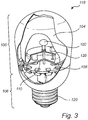
- the field emission lighting arrangement 118 is represented through a cross-section (i.e. side-view), where the evacuated envelope 100 and an anode structure 104 along an inside of the evacuated envelope 100 are shown.
- the anode structure 104 comprises a transparent electrically conducting layer and an electron to light conversion layer, such as a phosphor layer, e.g. using standard phosphors such as P22 (and/or e.g. quantum dots as mentioned above).
- a field emission cathode 102 having a slightly elliptical form is arranged along the optical axis 116 of the field emission lighting arrangement 118, and is arranged in the lower end of the evacuated envelope 100 adjacently to a base structure 106 of the field emission lighting arrangement 118.
- the field emission cathode 102 in the illustrated embodiment, and preferably according to the present invention has a circular form when seen from above (i.e. top-view, also visible from Fig. 3 ).
- the base structure 106 comprises a power supply 108 which is electrically connected (not shown) to the transparent electrical conductive layer of the anode structure 104 and to the cathode 102.
- the power supply may preferably deliver a DC (direct current) voltage to the anode structure 104 and the cathode 102.
- the field emission lighting arrangement 118 further comprises an electrically conductive structure 110 in the form of e.g. a conductive "shield", “foil” or “plate” being electrically connected (not shown) to the power supply 108.
- a first arrow 112 shows the distance from the cathode 102 to the anode structure 104 along the optical axis 116
- a second arrow 114 shows the distance from the cathode 102 to the anode structure 104 along another axis.
- the distance along the first arrow 112 is larger than along the second arrow 114, this is due to the shape and position of the cathode 102.
- the distance between the cathode 102 and the anode structure 104 decreases smooth and continuously as a function of the central angle from the optical axis 116 indicated by the second arrow 114.
- a typical pump stem 120 for the evacuated envelope 100 is additionally shown.
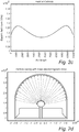
- Fig. 2a a graph of the electric field strength along a circumference of a cathode is shown; the electric field strength values (please note, absolute values are not of interest as they depend on the voltage applied) in Fig. 2a are calculated from spherical cathode geometry (i.e. a typical prior art field emission cathode).
- the arc length described starts at a -90degree angle from the optical axis and ends at a + 90 degree angle from the optical axis (as is indicated by the point-bolded line at the upper end surface of the cathode). It is apparent from Fig.
- Fig. 2c a graph of the electric field strength along a circumference comprising the optical axis of a cathode is shown, the electric field strength values in Fig. 2c are from an essentially ellipsoidal cathode, positioned in a more ideal manner below the centre of the half sphere part of the evacuated envelope (preferably between 0 - 5 mm below) according to the present invention, e.g. as shown in relation to the field emission lighting arrangement 118 of Fig. 1 .
- the electrical field strength along a circumference comprising the optical axis of a cathode according to the present invention will provide an (improved and) essentially uniform electrical field strength on the surface of the cathode as compared to the prior art illustration of Figs. 2a and 2b .
- the resulting field strength will, in use, provide essentially uniform distribution of the electrons emitted towards the anode structure.
- the electrons impinging upon the anode structure typically comprising the electron to light conversion layer, such as the phosphor layer
- the field uniformity may be greatly improved, as illustrated in Fig.2c to be around +/- 5%.
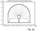
- the corresponding electron trajectories are adjusted in a corresponding manner such that they now cover almost the half sphere of the evacuated envelope.
- the electron trajectories are still further improved such that more than the half sphere will be covered by emitted electrons. This concept is further illustrated in Fig 2e .
- Fig. 3 represents a currently preferred embodiment of the field emission lighting arrangement 118 illustrated in Fig. 1 .
- the power supply 108 electrically connected to the cathode 102 and the anode structure 104 will supply a potential difference between the cathode 102 and the anode structure 104.
- Typical values of the potential difference are within the range of 4 - 12 kV, (the anode potential being "more" positive than the cathode potential) which will be adapted to the specific application and embodiment of the invention, smaller or larger potential differences might be preferred or other ranges are also within the scope of the invention.
- the potential difference will during operation of the field emission lighting arrangement 118 effect the emission of electrons from the cathode 102 towards the anode structure 104, the electrons impinging upon the anode structure 104, which comprises the above discussed transparent electrically conducting layer as well as the electron to light conversion layer, will first encounter the electron to light conversion layer and cause photons to be emitted from/by the electron to light conversion layer. The photons will travel through the transparent electrically conducting layer and will reach an observer, light a room or another area where light is desired.
- the cathode 102 in Fig. 3 is shaped and positioned according to the present invention, it has an elliptical shape and position within the evacuated envelope selected based on the bulb shaped evacuated envelope 100 in such a way that the uniformity of the electric field strength is improved which will provide an uniform spatial distribution of the light emitted from the field emission lighting arrangement 118. That is, the process for determining the shape of the field emission cathode 102 typically include determining the shape of the inside of the evacuated envelope 100 covered by the anode structure 104, determining a spatial relation as shown with the arrows of Fig.
- the electrically conductive structure 110 is shown in the currently preferred embodiment in Fig. 3 , being connected to the power supply 108 and biased by a potential adapted to the specific application.
- the electrically conductive structure 110 is configured to protect the power supply from electrons emitted by the cathode 102; by biasing the electrically conductive structure 110 with a potential further protection of the power supply 108 will be achieved. Another purpose of biasing the electrically conductive structure 110 with a potential might be further increase of the electric field strength.
- a connecting portion 120 of the base structure 106 is also included; the connecting portion is adapted to fit into a standard light bulb socket.
Landscapes
- Engineering & Computer Science (AREA)
- Manufacturing & Machinery (AREA)
- Discharge Lamps And Accessories Thereof (AREA)
- Vessels And Coating Films For Discharge Lamps (AREA)
- Cold Cathode And The Manufacture (AREA)
Claims (17)
- Agencement d'éclairage à émission de champ, comprenant :- une enveloppe évacuée en forme de bulbe, comprenant :- une cathode d'émission de champ agencée le long de l'axe optique de l'agencement d'éclairage à émission de champ, et- une structure d'anode agencée le long de l'intérieur de l'enveloppe évacuée, la structure d'anode comprenant une couche électroconductrice transparente et une couche de conversion d'électrons en lumière, et- une structure de base pourvue à une extrémité de fond de l'enveloppe évacuée, la structure de base comprenant une alimentation intégrée électriquement à l'intérieur de la structure de base et connectée à la structure d'anode et à la cathode, dans lequel l'alimentation est configurée pour appliquer une tension telle que des électrons sont émis de la cathode vers la structure d'anode, dans lequel la cathode d'émission de champ présente un facteur de forme essentiellement ellipsoïdal qui est sélectionné sur base d'une forme prédéterminée de l'enveloppe évacuée et est agencée dans une partie inférieure de l'enveloppe évacuée vers la structure de base, dans lequel la distance entre la surface de la cathode et la structure d'anode est la plus grande le long de l'axe optique et la distance la plus courte entre la surface de la cathode et la structure d'anode diminue quand augmente l'angle central à partir de l'axe optique.
- Agencement d'éclairage à émission de champ selon la revendication 1, dans lequel la distance entre la surface de la cathode et la structure d'anode varie entre 0,1 mm et 100 mm, de préférence entre 0,2 mm et 70 mm, et de manière préférée entre toutes entre 0,5 mm et 40 mm.
- Agencement d'éclairage à émission de champ selon la revendication 1 ou 2, dans lequel la cathode présente une section transversale essentiellement circulaire dans le plan dont la normale est alignée avec l'axe optique, et le ratio entre le demi-axe aligné avec la normale et les autres deux demi-axes est compris entre 1,05 et 2.
- Agencement d'éclairage à émission de champ selon l'une quelconque des revendications précédentes, dans lequel la sélection de la forme de cathode procure une grandeur de champ électrique qui varie de moins de 50 %, de préférence encore de moins de 20 %, et de manière préférée entre toutes de moins de 10 % en tous points de la surface de cathode.
- Agencement d'éclairage à émission de champ selon l'une quelconque des revendications précédentes, dans lequel la sélection de la forme de cathode procure des chemins d'électrons procurant une densité de courant électrique uniforme dans la structure d'anode.
- Agencement d'éclairage à émission de champ selon l'une quelconque des revendications précédentes, dans lequel l'agencement d'éclairage à émission de champ comprend en outre :- une structure électroconductrice agencée entre l'enveloppe évacuée et la structure de base.
- Agencement d'éclairage à émission de champ selon la revendication 6, dans lequel la structure électroconductrice est agencée à un potentiel électrique Vp par rapport à un potentiel électrique de la cathode Vc de telle sorte que Vp-Vc est positif, et sur base d'un potentiel électrique de la structure d'anode Va tel que (Vp-Vc)/(Va-Vc) est compris dans une plage de 0 à 2.
- Agencement d'éclairage à émission de champ selon l'une quelconque des revendications précédentes, dans lequel la cathode comprend en outre :- un réseau de structures de base saillantes agencées sur un substrat de la cathode, dans lequel les structures de base saillantes sont agencées pour présenter une distance centre à centre de 10 µm à 100 µm, de préférence encore de 10 µm à 60 µm, et de manière préférée entre toutes de 10 µm à 40 µm, et une hauteur de 5 µm à 60 µm, et- au moins une nanostructure agencée sur au moins une portion des structures de base saillantes.
- Agencement d'éclairage à émission de champ selon la revendication 8, dans lequel la nanostructure comprend au moins une nanotige de ZnO.
- Agencement d'éclairage à émission de champ selon la revendication 8, dans lequel la nanostructure comprend au moins un nanotube de carbone.
- Agencement d'éclairage à émission de champ selon la revendication 8, dans lequel les structures de base saillantes sont conformées comme des pyramides carrées.
- Agencement d'éclairage à émission de champ selon la revendication 11, dans lequel les structures de base saillantes conformées comme des pyramides carrées présentent une base de 10 µm à 100 µm.
- Agencement à émission de champ selon la revendication 1, dans lequel l'enveloppe évacuée en forme de bulbe est semi-sphérique, semi-parabolique ou semi-ellipsoïdale, et présente une connexion cylindrique, conique ou droite avec la structure de base.
- Agencement d'éclairage à émission de champ selon la revendication 8, dans lequel une pluralité de nanostructures est agencée de manière au moins partiellement aléatoire sur les structures de base.
- Procédé de sélection d'une forme de cathode d'émission de champ destinée à être utilisée dans un agencement d'éclairage à émission de champ, l'agencement d'éclairage à émission de champ comprenant :- une enveloppe évacuée en forme de bulbe comportant une structure d'anode agencée le long de l'intérieur de l'enveloppe évacuée, la structure d'anode comprenant une couche électroconductrice transparente et une couche de conversion d'électrons en lumière, et- une structure de base pourvue à une extrémité de fond de l'enveloppe évacuée, dans lequel la cathode d'émission de champ est agencée le long de l'axe optique de l'agencement d'éclairage à émission de champ et dans une partie inférieure de l'enveloppe évacuée vers la structure de base,dans lequel le procédé comprend :- la détermination d'une forme de l'intérieur de l'enveloppe évacuée recouverte par la structure d'anode ;- la détermination d'une relation spatiale entre la position où la cathode d'émission de champ est agencée dans la partie inférieure de l'enveloppe évacuée en corrélation avec la structure d'anode, et- la sélection de la forme de la cathode d'émission de champ pour qu'elle présente un facteur de forme essentiellement ellipsoïdal et de telle sorte que la distance entre la cathode d'émission de champ et la structure d'anode à l'intérieur de l'enveloppe évacuée est la plus grande le long de l'axe optique et la distance la plus courte entre la surface de la cathode et l'anode diminue quand augmente l'angle central à partir de l'axe optique.
- Procédé selon la revendication 15, dans lequel l'agencement d'éclairage à émission de champ comprend en outre une structure électroconductrice agencée entre l'enveloppe évacuée et la structure de base.
- Procédé selon l'une quelconque des revendications 15 et 16, comprenant en outre :- l'agencement d'un réseau de structures de base saillantes sur un substrat de la cathode, dans lequel les structures de base saillantes sont agencées pour présenter une distance centre à centre de 10 µm à 100 µm, de préférence encore de 10 µm à 60 µm, et de manière préférée entre toutes de 10 µm à 40 µm, et une hauteur de 5 µm à 60 µm ; et- l'agencement d'au moins une nanostructure sur au moins une portion des structures de base saillantes.
Priority Applications (7)
| Application Number | Priority Date | Filing Date | Title |
|---|---|---|---|
| EP13160768.1A EP2784800B1 (fr) | 2013-03-25 | 2013-03-25 | Cathode formée pour dispositif à émission de champ |
| PCT/EP2014/055124 WO2014154505A1 (fr) | 2013-03-25 | 2014-03-14 | Cathode profilée pour un agencement à émission de champ |
| JP2016503617A JP2016517143A (ja) | 2013-03-25 | 2014-03-14 | 電界放出装置の成形カソード |
| US14/773,582 US10043649B2 (en) | 2013-03-25 | 2014-03-14 | Shaped cathode for a field emission arrangement |
| CN201480017388.4A CN105051858B (zh) | 2013-03-25 | 2014-03-14 | 用于场发射装置的成形阴极 |
| TW103110065A TWI636479B (zh) | 2013-03-25 | 2014-03-18 | 場發射裝置之成形陰極及其形狀的選擇方法 |
| JP2018003568U JP3220295U (ja) | 2013-03-25 | 2018-09-12 | 電界放出装置の成形カソード |
Applications Claiming Priority (1)
| Application Number | Priority Date | Filing Date | Title |
|---|---|---|---|
| EP13160768.1A EP2784800B1 (fr) | 2013-03-25 | 2013-03-25 | Cathode formée pour dispositif à émission de champ |
Publications (2)
| Publication Number | Publication Date |
|---|---|
| EP2784800A1 EP2784800A1 (fr) | 2014-10-01 |
| EP2784800B1 true EP2784800B1 (fr) | 2018-12-05 |
Family
ID=47913255
Family Applications (1)
| Application Number | Title | Priority Date | Filing Date |
|---|---|---|---|
| EP13160768.1A Active EP2784800B1 (fr) | 2013-03-25 | 2013-03-25 | Cathode formée pour dispositif à émission de champ |
Country Status (6)
| Country | Link |
|---|---|
| US (1) | US10043649B2 (fr) |
| EP (1) | EP2784800B1 (fr) |
| JP (2) | JP2016517143A (fr) |
| CN (1) | CN105051858B (fr) |
| TW (1) | TWI636479B (fr) |
| WO (1) | WO2014154505A1 (fr) |
Families Citing this family (3)
| Publication number | Priority date | Publication date | Assignee | Title |
|---|---|---|---|---|
| EP3511974B1 (fr) | 2014-12-17 | 2021-02-24 | LightLab Sweden AB | Source lumineuse à émission de champ |
| EP3096341B1 (fr) * | 2015-05-18 | 2020-07-22 | LightLab Sweden AB | Procédé de fabrication de nanostructures pour une cathode à émission de champ |
| RU2658304C2 (ru) * | 2016-10-10 | 2018-06-20 | Акционерное общество "Научно-производственное предприятие "Алмаз" (АО "НПП "Алмаз") | Способ изготовления автоэмиссионного катода из углеродного материала |
Family Cites Families (22)
| Publication number | Priority date | Publication date | Assignee | Title |
|---|---|---|---|---|
| EP0035828A3 (fr) * | 1980-02-27 | 1982-01-27 | THE GENERAL ELECTRIC COMPANY, p.l.c. | Lampe d'éclairage électronique à fluorescence et circuit associé |
| US4818914A (en) | 1987-07-17 | 1989-04-04 | Sri International | High efficiency lamp |
| JP3226331B2 (ja) * | 1992-06-23 | 2001-11-05 | 松下電工株式会社 | 無電極放電灯点灯装置 |
| SE510413C2 (sv) * | 1997-06-13 | 1999-05-25 | Lightlab Ab | En fältemissionskatod och en ljuskälla innefattande en fältemissionskatod |
| SE515377C2 (sv) * | 1999-07-30 | 2001-07-23 | Nanolight Internat Ltd | Ljuskälla innefattande en fältemissionskatod |
| US20020070648A1 (en) * | 2000-12-08 | 2002-06-13 | Gunnar Forsberg | Field emitting cathode and a light source using a field emitting cathode |
| AU2002221226A1 (en) * | 2000-12-08 | 2002-06-18 | Lightlab Ab | A field emitting cathode and a light source using a field emitting cathode |
| JP2003346707A (ja) * | 2002-05-23 | 2003-12-05 | Noritake Co Ltd | 蛍光ランプ |
| SE0400156D0 (sv) * | 2004-01-29 | 2004-01-29 | Lightlab Ab | An anode in a field emission light source and a field emission light source comprising the anode |
| CN100543921C (zh) * | 2004-10-29 | 2009-09-23 | 清华大学 | 场发射发光照明光源 |
| JP4851735B2 (ja) * | 2005-06-14 | 2012-01-11 | 株式会社東芝 | 電界放出型冷陰極装置 |
| CN100573808C (zh) * | 2006-03-22 | 2009-12-23 | 清华大学 | 场发射照明光源及其制造方法 |
| TWI297169B (en) * | 2006-03-31 | 2008-05-21 | Hon Hai Prec Ind Co Ltd | Field emission illumination light source and method for making the same |
| JP2008108631A (ja) * | 2006-10-26 | 2008-05-08 | Kokusai Kiban Zairyo Kenkyusho:Kk | 電界放出型カソード基板、電界放出型光源および電界放出型表示素子 |
| US8294367B2 (en) * | 2007-02-05 | 2012-10-23 | Vu1 Corporation | System and apparatus for cathodoluminescent lighting |
| JP2009016281A (ja) * | 2007-07-09 | 2009-01-22 | Asahi Kasei Corp | 電界放出型電子放出素子 |
| CN101383264A (zh) * | 2007-09-07 | 2009-03-11 | 清华大学 | 场发射光源 |
| TWI364055B (en) * | 2007-10-12 | 2012-05-11 | Hon Hai Prec Ind Co Ltd | Field emission light source |
| JP2010062070A (ja) * | 2008-09-05 | 2010-03-18 | Rohm Co Ltd | 照明装置 |
| JP2010062069A (ja) * | 2008-09-05 | 2010-03-18 | Rohm Co Ltd | 炭素繊維装置 |
| EP2339610B1 (fr) * | 2009-12-22 | 2016-10-12 | LightLab Sweden AB | Structure d'anode réfléchissante pour un agencement d'éclairage à émission de champ |
| TWI456625B (zh) * | 2011-01-06 | 2014-10-11 | Tatung Co | 場發射燈 |
-
2013
- 2013-03-25 EP EP13160768.1A patent/EP2784800B1/fr active Active
-
2014
- 2014-03-14 US US14/773,582 patent/US10043649B2/en active Active
- 2014-03-14 CN CN201480017388.4A patent/CN105051858B/zh active Active
- 2014-03-14 WO PCT/EP2014/055124 patent/WO2014154505A1/fr active Application Filing
- 2014-03-14 JP JP2016503617A patent/JP2016517143A/ja active Pending
- 2014-03-18 TW TW103110065A patent/TWI636479B/zh active
-
2018
- 2018-09-12 JP JP2018003568U patent/JP3220295U/ja not_active Expired - Lifetime
Non-Patent Citations (1)
| Title |
|---|
| None * |
Also Published As
| Publication number | Publication date |
|---|---|
| EP2784800A1 (fr) | 2014-10-01 |
| JP3220295U (ja) | 2019-02-28 |
| JP2016517143A (ja) | 2016-06-09 |
| WO2014154505A1 (fr) | 2014-10-02 |
| TW201440109A (zh) | 2014-10-16 |
| US10043649B2 (en) | 2018-08-07 |
| US20160020084A1 (en) | 2016-01-21 |
| CN105051858B (zh) | 2017-06-30 |
| TWI636479B (zh) | 2018-09-21 |
| CN105051858A (zh) | 2015-11-11 |
Similar Documents
| Publication | Publication Date | Title |
|---|---|---|
| US7812511B2 (en) | Field emission illumination device | |
| US7728505B2 (en) | Field emission luminescent light source within a bulb | |
| US9006964B2 (en) | Field emission cathode | |
| US6873095B1 (en) | Light source, and a field emission cathode | |
| US8319413B2 (en) | Color field emission display having carbon nanotubes | |
| US8162711B2 (en) | Field emission display | |
| JP3220295U (ja) | 電界放出装置の成形カソード | |
| US7663298B2 (en) | Light source apparatus using field emission cathode | |
| US20020121856A1 (en) | Florescent lamps with extended service life | |
| US20170327372A1 (en) | Method for manufacturing nanostructures | |
| JP5354859B2 (ja) | 冷陰極蛍光ランプ | |
| EP3096341A1 (fr) | Procédé de fabrication de nanostructures pour une cathode à émission de champ | |
| TWI362674B (en) | Light source device | |
| JP2008153222A (ja) | 電界放出型ランプ | |
| Aban’shin et al. | Using carbon-containing field-emission structures in cathodoluminescent light sources | |
| KR20070118784A (ko) | 전자 방출 소자 | |
| JP2010244737A (ja) | 三極構造型の電界電子放出型ランプ及びその製造方法 |
Legal Events
| Date | Code | Title | Description |
|---|---|---|---|
| 17P | Request for examination filed |
Effective date: 20130325 |
|
| AK | Designated contracting states |
Kind code of ref document: A1 Designated state(s): AL AT BE BG CH CY CZ DE DK EE ES FI FR GB GR HR HU IE IS IT LI LT LU LV MC MK MT NL NO PL PT RO RS SE SI SK SM TR |
|
| AX | Request for extension of the european patent |
Extension state: BA ME |
|
| PUAI | Public reference made under article 153(3) epc to a published international application that has entered the european phase |
Free format text: ORIGINAL CODE: 0009012 |
|
| R17P | Request for examination filed (corrected) |
Effective date: 20150331 |
|
| RBV | Designated contracting states (corrected) |
Designated state(s): AL AT BE BG CH CY CZ DE DK EE ES FI FR GB GR HR HU IE IS IT LI LT LU LV MC MK MT NL NO PL PT RO RS SE SI SK SM TR |
|
| RAP1 | Party data changed (applicant data changed or rights of an application transferred) |
Owner name: LIGHTLAB SWEDEN AB |
|
| GRAP | Despatch of communication of intention to grant a patent |
Free format text: ORIGINAL CODE: EPIDOSNIGR1 |
|
| STAA | Information on the status of an ep patent application or granted ep patent |
Free format text: STATUS: GRANT OF PATENT IS INTENDED |
|
| INTG | Intention to grant announced |
Effective date: 20180907 |
|
| GRAS | Grant fee paid |
Free format text: ORIGINAL CODE: EPIDOSNIGR3 |
|
| GRAA | (expected) grant |
Free format text: ORIGINAL CODE: 0009210 |
|
| GRAA | (expected) grant |
Free format text: ORIGINAL CODE: 0009210 |
|
| STAA | Information on the status of an ep patent application or granted ep patent |
Free format text: STATUS: THE PATENT HAS BEEN GRANTED |
|
| AK | Designated contracting states |
Kind code of ref document: B1 Designated state(s): AL AT BE BG CH CY CZ DE DK EE ES FI FR GB GR HR HU IE IS IT LI LT LU LV MC MK MT NL NO PL PT RO RS SE SI SK SM TR |
|
| REG | Reference to a national code |
Ref country code: GB Ref legal event code: FG4D |
|
| REG | Reference to a national code |
Ref country code: CH Ref legal event code: EP |
|
| REG | Reference to a national code |
Ref country code: AT Ref legal event code: REF Ref document number: 1074105 Country of ref document: AT Kind code of ref document: T Effective date: 20181215 |
|
| REG | Reference to a national code |
Ref country code: IE Ref legal event code: FG4D |
|
| REG | Reference to a national code |
Ref country code: DE Ref legal event code: R096 Ref document number: 602013047676 Country of ref document: DE |
|
| REG | Reference to a national code |
Ref country code: SE Ref legal event code: TRGR |
|
| REG | Reference to a national code |
Ref country code: NL Ref legal event code: MP Effective date: 20181205 |
|
| REG | Reference to a national code |
Ref country code: AT Ref legal event code: MK05 Ref document number: 1074105 Country of ref document: AT Kind code of ref document: T Effective date: 20181205 |
|
| REG | Reference to a national code |
Ref country code: LT Ref legal event code: MG4D |
|
| PG25 | Lapsed in a contracting state [announced via postgrant information from national office to epo] |
Ref country code: FI Free format text: LAPSE BECAUSE OF FAILURE TO SUBMIT A TRANSLATION OF THE DESCRIPTION OR TO PAY THE FEE WITHIN THE PRESCRIBED TIME-LIMIT Effective date: 20181205 Ref country code: AT Free format text: LAPSE BECAUSE OF FAILURE TO SUBMIT A TRANSLATION OF THE DESCRIPTION OR TO PAY THE FEE WITHIN THE PRESCRIBED TIME-LIMIT Effective date: 20181205 Ref country code: NO Free format text: LAPSE BECAUSE OF FAILURE TO SUBMIT A TRANSLATION OF THE DESCRIPTION OR TO PAY THE FEE WITHIN THE PRESCRIBED TIME-LIMIT Effective date: 20190305 Ref country code: HR Free format text: LAPSE BECAUSE OF FAILURE TO SUBMIT A TRANSLATION OF THE DESCRIPTION OR TO PAY THE FEE WITHIN THE PRESCRIBED TIME-LIMIT Effective date: 20181205 Ref country code: LV Free format text: LAPSE BECAUSE OF FAILURE TO SUBMIT A TRANSLATION OF THE DESCRIPTION OR TO PAY THE FEE WITHIN THE PRESCRIBED TIME-LIMIT Effective date: 20181205 Ref country code: BG Free format text: LAPSE BECAUSE OF FAILURE TO SUBMIT A TRANSLATION OF THE DESCRIPTION OR TO PAY THE FEE WITHIN THE PRESCRIBED TIME-LIMIT Effective date: 20190305 Ref country code: LT Free format text: LAPSE BECAUSE OF FAILURE TO SUBMIT A TRANSLATION OF THE DESCRIPTION OR TO PAY THE FEE WITHIN THE PRESCRIBED TIME-LIMIT Effective date: 20181205 Ref country code: ES Free format text: LAPSE BECAUSE OF FAILURE TO SUBMIT A TRANSLATION OF THE DESCRIPTION OR TO PAY THE FEE WITHIN THE PRESCRIBED TIME-LIMIT Effective date: 20181205 |
|
| PG25 | Lapsed in a contracting state [announced via postgrant information from national office to epo] |
Ref country code: AL Free format text: LAPSE BECAUSE OF FAILURE TO SUBMIT A TRANSLATION OF THE DESCRIPTION OR TO PAY THE FEE WITHIN THE PRESCRIBED TIME-LIMIT Effective date: 20181205 Ref country code: GR Free format text: LAPSE BECAUSE OF FAILURE TO SUBMIT A TRANSLATION OF THE DESCRIPTION OR TO PAY THE FEE WITHIN THE PRESCRIBED TIME-LIMIT Effective date: 20190306 Ref country code: RS Free format text: LAPSE BECAUSE OF FAILURE TO SUBMIT A TRANSLATION OF THE DESCRIPTION OR TO PAY THE FEE WITHIN THE PRESCRIBED TIME-LIMIT Effective date: 20181205 |
|
| PG25 | Lapsed in a contracting state [announced via postgrant information from national office to epo] |
Ref country code: NL Free format text: LAPSE BECAUSE OF FAILURE TO SUBMIT A TRANSLATION OF THE DESCRIPTION OR TO PAY THE FEE WITHIN THE PRESCRIBED TIME-LIMIT Effective date: 20181205 |
|
| PG25 | Lapsed in a contracting state [announced via postgrant information from national office to epo] |
Ref country code: CZ Free format text: LAPSE BECAUSE OF FAILURE TO SUBMIT A TRANSLATION OF THE DESCRIPTION OR TO PAY THE FEE WITHIN THE PRESCRIBED TIME-LIMIT Effective date: 20181205 Ref country code: IT Free format text: LAPSE BECAUSE OF FAILURE TO SUBMIT A TRANSLATION OF THE DESCRIPTION OR TO PAY THE FEE WITHIN THE PRESCRIBED TIME-LIMIT Effective date: 20181205 Ref country code: PT Free format text: LAPSE BECAUSE OF FAILURE TO SUBMIT A TRANSLATION OF THE DESCRIPTION OR TO PAY THE FEE WITHIN THE PRESCRIBED TIME-LIMIT Effective date: 20190405 Ref country code: PL Free format text: LAPSE BECAUSE OF FAILURE TO SUBMIT A TRANSLATION OF THE DESCRIPTION OR TO PAY THE FEE WITHIN THE PRESCRIBED TIME-LIMIT Effective date: 20181205 |
|
| PG25 | Lapsed in a contracting state [announced via postgrant information from national office to epo] |
Ref country code: SM Free format text: LAPSE BECAUSE OF FAILURE TO SUBMIT A TRANSLATION OF THE DESCRIPTION OR TO PAY THE FEE WITHIN THE PRESCRIBED TIME-LIMIT Effective date: 20181205 Ref country code: EE Free format text: LAPSE BECAUSE OF FAILURE TO SUBMIT A TRANSLATION OF THE DESCRIPTION OR TO PAY THE FEE WITHIN THE PRESCRIBED TIME-LIMIT Effective date: 20181205 Ref country code: SK Free format text: LAPSE BECAUSE OF FAILURE TO SUBMIT A TRANSLATION OF THE DESCRIPTION OR TO PAY THE FEE WITHIN THE PRESCRIBED TIME-LIMIT Effective date: 20181205 Ref country code: RO Free format text: LAPSE BECAUSE OF FAILURE TO SUBMIT A TRANSLATION OF THE DESCRIPTION OR TO PAY THE FEE WITHIN THE PRESCRIBED TIME-LIMIT Effective date: 20181205 Ref country code: IS Free format text: LAPSE BECAUSE OF FAILURE TO SUBMIT A TRANSLATION OF THE DESCRIPTION OR TO PAY THE FEE WITHIN THE PRESCRIBED TIME-LIMIT Effective date: 20190405 |
|
| REG | Reference to a national code |
Ref country code: DE Ref legal event code: R097 Ref document number: 602013047676 Country of ref document: DE |
|
| PLBE | No opposition filed within time limit |
Free format text: ORIGINAL CODE: 0009261 |
|
| STAA | Information on the status of an ep patent application or granted ep patent |
Free format text: STATUS: NO OPPOSITION FILED WITHIN TIME LIMIT |
|
| PG25 | Lapsed in a contracting state [announced via postgrant information from national office to epo] |
Ref country code: DK Free format text: LAPSE BECAUSE OF FAILURE TO SUBMIT A TRANSLATION OF THE DESCRIPTION OR TO PAY THE FEE WITHIN THE PRESCRIBED TIME-LIMIT Effective date: 20181205 Ref country code: MC Free format text: LAPSE BECAUSE OF FAILURE TO SUBMIT A TRANSLATION OF THE DESCRIPTION OR TO PAY THE FEE WITHIN THE PRESCRIBED TIME-LIMIT Effective date: 20181205 Ref country code: SI Free format text: LAPSE BECAUSE OF FAILURE TO SUBMIT A TRANSLATION OF THE DESCRIPTION OR TO PAY THE FEE WITHIN THE PRESCRIBED TIME-LIMIT Effective date: 20181205 |
|
| REG | Reference to a national code |
Ref country code: CH Ref legal event code: PL |
|
| 26N | No opposition filed |
Effective date: 20190906 |
|
| PG25 | Lapsed in a contracting state [announced via postgrant information from national office to epo] |
Ref country code: LU Free format text: LAPSE BECAUSE OF NON-PAYMENT OF DUE FEES Effective date: 20190325 |
|
| REG | Reference to a national code |
Ref country code: BE Ref legal event code: MM Effective date: 20190331 |
|
| PG25 | Lapsed in a contracting state [announced via postgrant information from national office to epo] |
Ref country code: CH Free format text: LAPSE BECAUSE OF NON-PAYMENT OF DUE FEES Effective date: 20190331 Ref country code: LI Free format text: LAPSE BECAUSE OF NON-PAYMENT OF DUE FEES Effective date: 20190331 Ref country code: IE Free format text: LAPSE BECAUSE OF NON-PAYMENT OF DUE FEES Effective date: 20190325 |
|
| PG25 | Lapsed in a contracting state [announced via postgrant information from national office to epo] |
Ref country code: BE Free format text: LAPSE BECAUSE OF NON-PAYMENT OF DUE FEES Effective date: 20190331 |
|
| PG25 | Lapsed in a contracting state [announced via postgrant information from national office to epo] |
Ref country code: TR Free format text: LAPSE BECAUSE OF FAILURE TO SUBMIT A TRANSLATION OF THE DESCRIPTION OR TO PAY THE FEE WITHIN THE PRESCRIBED TIME-LIMIT Effective date: 20181205 |
|
| PG25 | Lapsed in a contracting state [announced via postgrant information from national office to epo] |
Ref country code: MT Free format text: LAPSE BECAUSE OF NON-PAYMENT OF DUE FEES Effective date: 20190325 |
|
| PG25 | Lapsed in a contracting state [announced via postgrant information from national office to epo] |
Ref country code: CY Free format text: LAPSE BECAUSE OF FAILURE TO SUBMIT A TRANSLATION OF THE DESCRIPTION OR TO PAY THE FEE WITHIN THE PRESCRIBED TIME-LIMIT Effective date: 20181205 |
|
| PG25 | Lapsed in a contracting state [announced via postgrant information from national office to epo] |
Ref country code: HU Free format text: LAPSE BECAUSE OF FAILURE TO SUBMIT A TRANSLATION OF THE DESCRIPTION OR TO PAY THE FEE WITHIN THE PRESCRIBED TIME-LIMIT; INVALID AB INITIO Effective date: 20130325 |
|
| PG25 | Lapsed in a contracting state [announced via postgrant information from national office to epo] |
Ref country code: MK Free format text: LAPSE BECAUSE OF FAILURE TO SUBMIT A TRANSLATION OF THE DESCRIPTION OR TO PAY THE FEE WITHIN THE PRESCRIBED TIME-LIMIT Effective date: 20181205 |
|
| REG | Reference to a national code |
Ref country code: DE Ref legal event code: R081 Ref document number: 602013047676 Country of ref document: DE Owner name: PUREFIZE TECHNOLOGIES AB, SE Free format text: FORMER OWNER: LIGHTLAB SWEDEN AB, UPPSALA, SE |
|
| PGFP | Annual fee paid to national office [announced via postgrant information from national office to epo] |
Ref country code: FR Payment date: 20230314 Year of fee payment: 11 |
|
| PGFP | Annual fee paid to national office [announced via postgrant information from national office to epo] |
Ref country code: SE Payment date: 20230314 Year of fee payment: 11 |
|
| PGFP | Annual fee paid to national office [announced via postgrant information from national office to epo] |
Ref country code: DE Payment date: 20240319 Year of fee payment: 12 Ref country code: GB Payment date: 20240318 Year of fee payment: 12 |