EP2783383B1 - Elektronenemittierende kaltkathodenvorrichtung - Google Patents
Elektronenemittierende kaltkathodenvorrichtung Download PDFInfo
- Publication number
- EP2783383B1 EP2783383B1 EP12808505.7A EP12808505A EP2783383B1 EP 2783383 B1 EP2783383 B1 EP 2783383B1 EP 12808505 A EP12808505 A EP 12808505A EP 2783383 B1 EP2783383 B1 EP 2783383B1
- Authority
- EP
- European Patent Office
- Prior art keywords
- cathode
- gate
- straight
- finger
- insulating substrate
- Prior art date
- Legal status (The legal status is an assumption and is not a legal conclusion. Google has not performed a legal analysis and makes no representation as to the accuracy of the status listed.)
- Not-in-force
Links
Images




Classifications
-
- H—ELECTRICITY
- H01—ELECTRIC ELEMENTS
- H01J—ELECTRIC DISCHARGE TUBES OR DISCHARGE LAMPS
- H01J19/00—Details of vacuum tubes of the types covered by group H01J21/00
- H01J19/02—Electron-emitting electrodes; Cathodes
- H01J19/24—Cold cathodes, e.g. field-emissive cathode
-
- H—ELECTRICITY
- H01—ELECTRIC ELEMENTS
- H01J—ELECTRIC DISCHARGE TUBES OR DISCHARGE LAMPS
- H01J1/00—Details of electrodes, of magnetic control means, of screens, or of the mounting or spacing thereof, common to two or more basic types of discharge tubes or lamps
- H01J1/02—Main electrodes
- H01J1/30—Cold cathodes, e.g. field-emissive cathode
- H01J1/304—Field-emissive cathodes
- H01J1/3042—Field-emissive cathodes microengineered, e.g. Spindt-type
-
- H—ELECTRICITY
- H01—ELECTRIC ELEMENTS
- H01J—ELECTRIC DISCHARGE TUBES OR DISCHARGE LAMPS
- H01J19/00—Details of vacuum tubes of the types covered by group H01J21/00
- H01J19/28—Non-electron-emitting electrodes; Screens
- H01J19/32—Anodes
-
- H—ELECTRICITY
- H01—ELECTRIC ELEMENTS
- H01J—ELECTRIC DISCHARGE TUBES OR DISCHARGE LAMPS
- H01J19/00—Details of vacuum tubes of the types covered by group H01J21/00
- H01J19/28—Non-electron-emitting electrodes; Screens
- H01J19/38—Control electrodes, e.g. grid
-
- H—ELECTRICITY
- H01—ELECTRIC ELEMENTS
- H01J—ELECTRIC DISCHARGE TUBES OR DISCHARGE LAMPS
- H01J19/00—Details of vacuum tubes of the types covered by group H01J21/00
- H01J19/42—Mounting, supporting, spacing, or insulating of electrodes or of electrode assemblies
- H01J19/46—Mountings for the electrode assembly as a whole
-
- H—ELECTRICITY
- H01—ELECTRIC ELEMENTS
- H01J—ELECTRIC DISCHARGE TUBES OR DISCHARGE LAMPS
- H01J21/00—Vacuum tubes
- H01J21/02—Tubes with a single discharge path
- H01J21/06—Tubes with a single discharge path having electrostatic control means only
- H01J21/10—Tubes with a single discharge path having electrostatic control means only with one or more immovable internal control electrodes, e.g. triode, pentode, octode
- H01J21/105—Tubes with a single discharge path having electrostatic control means only with one or more immovable internal control electrodes, e.g. triode, pentode, octode with microengineered cathode and control electrodes, e.g. Spindt-type
-
- H—ELECTRICITY
- H01—ELECTRIC ELEMENTS
- H01J—ELECTRIC DISCHARGE TUBES OR DISCHARGE LAMPS
- H01J21/00—Vacuum tubes
- H01J21/20—Tubes with more than one discharge path; Multiple tubes, e.g. double diode, triode-hexode
-
- H—ELECTRICITY
- H01—ELECTRIC ELEMENTS
- H01J—ELECTRIC DISCHARGE TUBES OR DISCHARGE LAMPS
- H01J3/00—Details of electron-optical or ion-optical arrangements common to two or more basic types of discharge tubes or lamps
- H01J3/02—Electron guns
- H01J3/021—Electron guns using a field emission, photo emission, or secondary emission electron source
- H01J3/022—Electron guns using a field emission, photo emission, or secondary emission electron source with microengineered cathode, e.g. Spindt-type
-
- H—ELECTRICITY
- H01—ELECTRIC ELEMENTS
- H01J—ELECTRIC DISCHARGE TUBES OR DISCHARGE LAMPS
- H01J9/00—Apparatus or processes specially adapted for the manufacture, installation, removal, maintenance of electric discharge tubes, discharge lamps, or parts thereof; Recovery of material from discharge tubes or lamps
- H01J9/02—Manufacture of electrodes or electrode systems
- H01J9/022—Manufacture of electrodes or electrode systems of cold cathodes
- H01J9/025—Manufacture of electrodes or electrode systems of cold cathodes of field emission cathodes
Definitions
- the present invention relates, in general, to a micrometric/nanometric electronic device belonging to the family of semiconductor vacuum tubes for high-frequency applications and, in particular, to an electron-emitting cold cathode device for high-frequency applications. More specifically, the present invention concerns a cold-cathode triode and a cold-cathode electron gun.
- vacuum electronics instead of semiconductor technology allows the property of electrons to reach higher speeds in a vacuum than in a semiconductor material to be exploited and, in consequence, to achieve higher operating frequencies (nominally from GHz to THz).
- the general working principle of vacuum electronic devices is based on the interaction between a radio frequency (RF) signal and a generated electron beam; the RF signal imposes velocity modulation on the electrons in the electron beam, permitting an energy transfer from the electron beam to the RF signal.
- RF radio frequency
- FEA Field Emission Array
- Spindt cathode devices exploit micromachined metal electron emitter tips or cones formed on a conductive substrate and in ohmic contact therewith.
- Each emitter has its own concentric aperture in an acceleration field between an anode electrode and a cathode electrode.
- a gate electrode also known as a control or modulation grid, is isolated from the anode and cathode electrodes and from the emitters by a silicon dioxide layer.
- Large arrays of electron emitter tips, each capable of producing several tens of microamperes, can theoretically produce large emission current densities.
- the Spindt structure has been greatly improved by using carbon nanotubes (CNTs) as cold cathode emitters (see, for example, S. Iijima, Helical microtubules of graphitic carbon, Nature, 1991, volume 354, pages 56-58 , or W. Heer, A. Chatelain, D. Ugarte, A carbon nanotube field-emission electron source, Science, 1995, volume 270, issue 5239, pages 1179-1180 ).
- CNTs carbon nanotubes
- Carbon nanotubes are perfectly graphitized cylindrical tubes that can be produced with diameters ranging from approximately 2 to 100 nm and lengths of several microns, using various manufacturing processes.
- CNTs can be considered as being among the best emitters in nature (see, for example, J. M. Bonard, J.P. Salvetat, T. Stockli, L. Forr ⁇ and A. Cegolain, Field emission from carbon nanotubes: perspectives for applications and clues to the emission mechanism, Applied Physics A, 1999, volume 69, pages 245-254 ), and therefore are ideal electron emitters in a Spindt-type device; many studies have already acknowledged their field emission properties (see, for example, S. Orlanducci, V. Sessa, M. L. Terranova, M. Rossi and D. Manno, Chinese Physics Letters, 2003, volume 367, pages 109-114 ).
- Figure 1 shows a schematic cross-sectional view of a known Spindt-type cold cathode device, in particular a Spindt-type cold-cathode triode, which uses the CNTs as electron emitters and which is indicated as a whole in Figure 1 by reference numeral 1.
- the triode 1 comprises:
- the cathode structure 2 with the integrated gate electrode 5 and the anode electrode 3 are formed separately and then bonded together with the interposition of the lateral spacers 4.
- the anode electrode 3 is made up of a first conductive substrate that functions as the anode of the triode device 1, while the cathode structure 2 is a multilayer structure that comprises:
- biasing the gate electrode 5 allows controlling the flow of electrons generated by the cathode structure 2 towards the node electrode 3 in the area corresponding to and surrounding the recess 9; the current thus generated is collected by the portion of the anode electrode 3 that is placed over the gate electrode 5.
- the topographical configuration of Spindt-type cold-cathode triodes suffers from an important limitation caused by high parasitic capacitances existing between the gate electrode and the cathode and anode electrodes. These parasitic capacitances heavily limit the operating frequencies that this type of device can reach, reducing the cut-off frequencies and rendering THz applications substantially unfeasible, even for micron-scaled structures.
- these parasitic capacitances are due to the overlapping of the gate, cathode and anode electrodes.
- a topographical configuration for vacuum devices with a Spindt-type FEA cathode that partially reduces the aforementioned parasitic capacitances is described by C. A. Spindt, C. E. Holland, A. Rosengreen and I. Brodie in Field-emitter-array development for high-frequency operation, Journal of Vacuum Science & Technology B: Microelectronics and Nanometer Structures, Volume 11, Issue 2, March 1993, pages 468-473 .
- Field-emitter-array development for high-frequency operation describes a Spindt-type cold-cathode triode in which the cathode and gate electrodes only overlap in the active areas of the triode (regarding this, please refer specifically to Figures 2 and 4 of said article).
- the triode structure presented in Field-emitter-array development for high-frequency operation permits achieving operating frequencies in the order of gigahertz (GHz), while, because of the residual parasitic capacitances due to the overlapping of the cathode and gate electrodes in the active area, this triode structure does not allow frequencies in the THz band to be reached.
- GHz gigahertz
- European Patent EP2223325 granted to the applicant also describes an innovative topographical configuration for Spindt-type cold-cathode triodes that enables the aforementioned parasitic capacitances to be reduced.
- EP2223325 describes a triode, in particular for high-frequency applications, comprising a multilayer structure that includes:
- a second type of vacuum devices is the so-called electron gun.
- an electron gun is a device that produces an electron beam with precise kinetic energy and can be used:
- an electron gun comprises:
- the cathode structure In use, the cathode structure generates an electron beam, the focusing grid focuses the electron beam generated by the cathode structure onto the hole of the anode structure, the anode structure accelerates and focuses the electron beam that passes through the hole still further due to a large potential difference with respect to the focusing grid, while the collector receives the flow of electrons that leaves the hole of the anode structure.
- a modulation grid (or gate electrode) can be conveniently integrated into the cathode structure of an electron gun.
- the emitted current can be directly modulated by applying an RF signal on said modulation grid.
- Direct modulation of the emitted current has already been used on thermionic cathodes (see, for example, A. J. Lichtenberg, Prebunched beam traveling wave tube studies, IRE Trans. Electron Devices, 1962, vol. ED-9, pages 345-351 ), in this way obtaining advantages in terms of vacuum tube efficiency and gain.
- Prebunched beam traveling wave tube studies a 20% to 35% increase in the efficiency of a TWT amplifier by using a frequency-modulated thermionic cathode is described.
- the modulation is limited to a maximum of 2 GHz in this type of vacuum tube because of the large distance between cathode and modulation grid.
- European patent application EP 2 113 934 A2 describes an electron source for an image display apparatus in which the electron source comprises a plurality of electron emitter devices connected to a matrix wiring of scanning lines and modulation lines on a substrate.
- each of the electron emitter devices comprises a cathode electrode connected to a scanning line, a gate electrode connected to a modulation line and a plurality of electron emitter members.
- EP 2 113 934 A2 has a very "angular" structure with many right angles.
- the Applicant has carried out in-depth research for the purpose of developing a topographical configuration for electron-emitting cold cathode devices that enables, in general, the drawbacks of known electron-emitting cold cathode devices to be at least partially mitigated and, in particular, to increase the operating frequencies of electron-emitting cold cathode devices.
- the present invention relates to an electron-emitting cold cathode device.
- the electron-emitting cold cathode device comprises:
- the cathode electrode also comprises a cathode conduction line that is (directly or indirectly) connected to the cathode fingered structure, has a straight-strip-like shape with a main extension direction parallel to the first reference direction and is symmetrical with respect to an axis of symmetry of the cathode parallel to the first reference direction. Furthermore, the cathode fingered structure is also symmetrical with respect to said axis of symmetry of the cathode.
- the gate electrode also comprises a gate conduction line that is (directly or indirectly) connected to the gate fingered structure, has a straight-strip-like shape with a main extension direction parallel to the first reference direction and is symmetrical with respect to an axis of symmetry of the gate parallel to the first reference direction. Furthermore, the gate fingered structure is also symmetrical with respect to said axis of symmetry of the gate.
- the respective electron emitter(s) is/are substantially median with respect to said cathode straight-finger-shaped terminal, in particular the electron emitter(s) is/are placed in position(s) that is/are substantially median with respect to said cathode straight-finger-shaped terminal, precision of the manufacturing technology permitting.
- Each cathode straight-finger-shaped terminal is contained between two gate straight-finger-shaped terminals and, for each cathode straight-finger-shaped terminal, the respective electron emitter(s) is/are substantially median with respect to the two adjacent gate straight-finger-shaped terminals.
- the present invention enables increasing the operating frequencies of electron-emitting cold cathode devices.
- the present invention enables producing electron-emitting cold cathode devices capable of operating at THz frequencies.
- a first preferred embodiment of the present invention relates to a triode with a cold-cathode electron emitter.
- the cold-cathode triode 11 comprises:
- the cathode electrode 14, which is designed to emit electrons in the direction of the anode electrode 17, in particular towards the anode terminal 17a, is formed on a portion of the recessed top surface of the first electrically insulating substrate 13 and comprises:
- the cathode electrode 14 has a rake-like shape, in which the cathode straight-finger-shaped terminals 14b are the rake teeth, the cathode backbone line 14d is the base of the rake from which said teeth extend and the cathode conduction line 14e is the rake handle that extends from said base.
- the cathode conduction line 14e can be conveniently placed on and along an axis of symmetry of the cathode backbone line 14d that is parallel to the longitudinal reference direction z, and the cathode multi-fingered structure 14a can conveniently be symmetrical with respect to said axis of symmetry of the cathode backbone line 14d.
- cathode straight-finger-shaped terminals 14b will be called cathode fingers for simplicity of description.
- the cathode backbone line 14d may not be present and the cathode fingers 14b can protrude, or rather extend, directly from one end of the cathode conduction line 14e.
- the cathode multi-fingered structure 14a can conveniently be symmetrical with respect to an axis of symmetry of the cathode conduction line 14e that is parallel to the longitudinal reference direction z.
- the gate electrode 15, which is designed to control, or modulate, the flow of electrons between the electron emitters 14c and the anode terminal 17a, is formed on a portion of the raised top surface of the first electrically insulating substrate 13 and comprises:
- the gate electrode 15 has a rake-like shape in which the gate straight-finger-shaped terminals 15b are the rake teeth, the gate backbone line 15c is the base of the rake from which said teeth extend and the gate conduction line 15d is the rake handle that extends from said base in the opposite direction to that of the extension of the cathode electrode 14.
- the gate conduction line 15d can be conveniently placed on and along the axis of symmetry of the gate backbone line 15c that is parallel to the longitudinal reference direction z, and the gate multi-fingered structure 15a can conveniently be symmetrical with respect to said axis of symmetry of the gate backbone line 15c.
- gate straight-finger-shaped terminals 15b will be called gate fingers for simplicity of description.
- the gate backbone line 15c may not be present and the gate fingers 15b can protrude, or rather extend, directly from one end of the gate conduction line 15d.
- the gate multi-fingered structure 15a can conveniently be symmetrical with respect to an axis of symmetry of the gate conduction line 15d that is parallel to the longitudinal reference direction z.
- the cathode fingers 14b and gate fingers 15b are mutually interlaced, in particular interfingered, that the cathode electrode 14 and gate electrode 15 do not overlap in any region of the triode 11, that, specifically, the cathode fingers 14b and gate fingers 15b are interlaced in the active region 11a and therefore not overlapping, and that the cathode conduction line 14e and gate conduction line 15d have opposite respective main extension directions that (if projected onto any reference plane parallel to the ground plane 12) form an angle of 180° between them.
- the cathode electrode 14 and gate electrode 15 are not overlapping, in particular thanks to the fact that in the active region 11a, the cathode fingers 14b and gate fingers 15b are not overlapping, parasitic capacitances between the cathode electrode 14 and gate electrode 15 are significantly reduced, or even completely eliminated.
- the geometry of the cathode electrode 14 and the gate electrode 15 makes the manufacturing process of these electrodes extremely simple and easily reproducible.
- Figure 4 a schematic top view is shown of a portion of just the first electrically insulating substrate 13 before the cathode 14 and gate 15 contacts are formed, where the same reference numerals indicate the same elements shown in Figures 2 and 3 and previously described, and where the dimensions shown are not to scale for simplicity of illustration.
- Figure 4 partially shows:
- the raised top surface 13c comprises:
- the multi-fingered raised surface can conveniently be symmetrical with respect to an axis of symmetry of the second raised area 13g that is parallel to the longitudinal reference direction z.
- the recessed top surface 13b comprises:
- the multi-fingered recessed surface can conveniently be symmetrical with respect to an axis of symmetry of the second recessed area 13e that is parallel to the longitudinal reference direction z.
- Figures 5 and 6 respectively show a schematic top view and a schematic, longitudinal sectional view of a portion of the first electrically insulating substrate 13 on which the cathode 14 and gate 15 contacts are formed
- Figure 7 shows a schematic cross-sectional view of a portion of the active region 11a.
- the cathode multi-fingered structure 14a is formed on the multi-fingered recessed surface at the active region 11a and, specifically:
- the gate multi-fingered structure 15a is also formed on the multi-fingered raised surface at the active region 11a and, specifically:
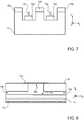
- Figure 8 shows a schematic, longitudinal sectional view of the triode 11
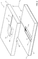
- Figure 9 shows a perspective top view of a central portion of the triode 11.
- the second recess 16a which has a main extension dimension parallel to the longitudinal reference direction z, longitudinally crosses the entire lower surface of the second electrically insulating substrate 16, preferably so as to divide said lower surface into two equal and symmetrical portions, i.e. so as to define an axis of symmetry of said lower surface of the second electrically insulating substrate 16 that is parallel to the longitudinal reference direction z.
- the third recess 16b which has a main extension dimension parallel to the vertical reference direction y, vertically crosses the entire second electrically insulating substrate 16, starting from the second recess 16a and arriving to the top surface of said second electrically insulating substrate 16.
- the third recess 16b is positioned at, and consequently passes vertically through, a central region of the second electrically insulating substrate 16.
- the second electrically insulating substrate 16 is bonded onto the first electrically insulating substrate 13, using vacuum bonding techniques, in order to maintain electrical insulation in the middle.
- the second electrically insulating substrate 16 is bonded to the first electrically insulating substrate 13 using standard wafer-to-wafer vacuum bonding techniques, such as anodic bonding, glass frit bonding, eutectic bonding, solder bonding, reactive bonding or fusion bonding.
- the second electrically insulating substrate 16 is bonded onto the first electrically insulating substrate 13 so that:
- anode electrode 17 comprises:
- the anode electrode 17 only partially overlaps the cathode electrode 14 and gate electrode 15. Specifically, the anode terminal 17a is placed over the cathode fingers 14b, gate fingers 15b, cathode backbone line 14d and gate backbone line 15c and just partially overlaps the cathode conduction line 14e and gate conduction line 15d, while the anode conduction line 17b overlaps neither the cathode electrode 14 nor the gate electrode 15.
- the geometry of the anode electrode 17 makes the manufacturing process of this electrode extremely simple and easily reproducible.
- triode 11 With regard to the size of the triode 11 described so far, said triode 11 can conveniently have the dimensions indicated below.
- the first electrically insulating substrate 13 can conveniently have a substantially rectangular or square shape in plan (i.e. parallel to the ground plane 12) with lateral dimensions in the order of a few millimetres.
- said first electrically insulating substrate 13 can have, parallel to the longitudinal reference direction z, a length that is equal to or greater than 4 mm.
- said first electrically insulating substrate 13 can conveniently have a thickness (parallel to the vertical reference direction y) of between 200 ⁇ m and 1 mm, preferably, in order to make the triode 11 operate at THz frequencies, between 200 ⁇ m and 500 ⁇ m.
- the offset, or rather the vertical distance (i.e. parallel to the vertical reference direction y), between the recessed top surface 13b and the raised top surface 13c of the first electrically insulating substrate 13 can conveniently be between 0.5 ⁇ m and a few tens of microns, in particular between 0.5 ⁇ m and 15 ⁇ m.
- said offset should be between 0.5 ⁇ m and 5 ⁇ m.
- the thickness (parallel to the vertical reference direction y) of the cathode electrode 14 and gate electrode 15 can be between 50 nm and 300 nm.
- said thickness of the cathode electrode 14 and gate electrode 15 can be between 50 nm and 100 nm.
- the cathode fingers 14b and gate fingers 15b can conveniently have, parallel to the transversal reference direction x, a width between a minimum of a hundred nanometres and a maximum of a few micron, according to the manufacturing technology employed (optical or e-beam photolithography).
- said width of the cathode fingers 14b and gate fingers 15b can be between 0.1 ⁇ m and 20 ⁇ m.
- said width of the cathode fingers 14b and gate fingers 15b can conveniently be between 0.1 ⁇ m and 1 ⁇ m.
- Each cathode finger 14b can be conveniently spaced apart laterally (or rather, parallel to the transversal reference direction x) from the corresponding first raised areas 13f, between which said cathode finger 14b is contained (i.e. from the corresponding gate fingers 15b that are immediately adjacent to said cathode finger 14b), by a distance of between 0.3 ⁇ m and 20 ⁇ m, preferably, in order to make the triode 11 operate at THz frequencies, between 0.3 ⁇ m and 3 ⁇ m.
- the number of cathode fingers 14b and gate fingers 15b can be conveniently comprised between a minimum of a few units and a maximum of a few tens.
- the cathode conduction line 14e and gate conduction line 15d can conveniently have, parallel to the transversal reference direction x, a width of between 20 ⁇ m and 1020 ⁇ m, preferably, in order to make the triode 11 operate at THz frequencies, between 20 ⁇ m and 100 ⁇ m, so as to be able to connect the triode 11 externally by wire bonding.
- the active region 11a can conveniently have, parallel to the longitudinal reference direction z, a length of between 20 ⁇ m and 500 ⁇ m, preferably, in order to make the triode 11 operate at THz frequencies, between 20 ⁇ m and 100 ⁇ m.
- the electron emitters 14c can conveniently have, parallel to the vertical reference direction y, a height substantially equal to the height of the dielectric between the cathode fingers 14b and gate fingers 15b, so as to optimize the transconductance of the triode 11 as much as possible.
- the second electrically insulating substrate 16 can conveniently have a substantially rectangular or square shape in plan (i.e. parallel to the ground plane 12) with lateral dimensions substantially equal to those of the first electrically insulating substrate 13.
- the thickness (parallel to the vertical reference direction y) of said second electrically insulating substrate 16 can conveniently be in the order of a few hundreds of microns, so as to be able to use extraction voltages that are not too high.
- the thickness of said second electrically insulating substrate 16 can be between 100 ⁇ m and 500 ⁇ m.
- the thickness of said second electrically insulating substrate 16 can conveniently be between 100 ⁇ m and 300 ⁇ m.
- the third recess 16b can conveniently have a substantially rectangular or square shape in plan (i.e. parallel to the ground plane 12) with lateral dimensions having respective values between a minimum of a few hundred microns and a maximum of a few millimetres.
- the third recess 16b can have, parallel to the longitudinal reference direction z, a length of between 0.5 mm and 2 mm.
- the third recess 16b can conveniently have, parallel to the longitudinal reference direction z, a length of between 0.3 mm and 1.5 mm.
- the anode terminal 17a can conveniently have a substantially rectangular or square shape in plan (i.e. parallel to the ground plane 12) with lateral dimensions having respective values between a minimum of 0.5 mm and a maximum of a few millimetres.
- the following table concisely lists the values of characteristic impedance Z 0 and propagation loss ⁇ for the cathode conduction line 14e and gate conduction line 15d that correspond to different widths W (parallel to the transversal reference direction x) of said cathode conduction line 14e and gate conduction line 15d and to different thicknesses H (parallel to the vertical reference direction y) of the first electrically insulating substrate 13, under the assumption that said first electrically insulating substrate 13 has a relative electric permittivity (or relative dielectric constant) ⁇ r equal to 4 and that said cathode conduction line 14e and gate conduction line 15d have a thickness T (parallel to the vertical reference direction y) equal to 300 nm.
- the first electrically insulating substrate 13 and the second electrically insulating substrate 16 can be conveniently made using initial substrates in Pyrex glass, or fused silica, or float glass, or quartz.
- the cathode electrode 14 and gate electrode 15 do not overlap in any region of the triode 11 and that, specifically, the cathode fingers 14b and gate fingers 15b are interlaced, and therefore not overlapped, in the active region 11a.
- This feature of the triode 11 enables parasitic capacitances between the cathode electrode 14 and gate electrode 15 to be significantly reduced or even completely eliminated and genuinely extends the operating frequency band of the triode 11 into the THz range.
- the geometry of the cathode electrode 14 and the gate electrode 15, in particular thanks to the cathode straight-finger-shaped terminals 14b, the gate straight-finger-shaped terminals 15b, the straight cathode conduction line 14e and the straight gate conduction line 15d, enables the operating frequency band of the triode 11 to be genuinely extended to the THz range.
- anode electrode 17 is only partially overlapping the cathode electrode 14 and gate electrode 15 (in particular, only the anode terminal 17a fully overlaps the cathode fingers 14b, gate fingers 15b, cathode backbone line 14d and gate backbone line 15c and just partially overlaps the cathode conduction line 14e and gate conduction line 15d), parasitic capacitances between the anode electrode 17 and the cathode electrode 14 and gate electrode 15 are also significantly reduced.
- the cathode conduction line 14e and gate conduction line 15d have respective main extension directions that (if projected on any reference plane parallel to the ground plane 12) form an angle of 180° between them and the fact that the anode conduction line 17b has a main extension direction that forms a respective 90° angle with each of the main extension directions of the cathode conduction line 14e and gate conduction line 15d (if said directions are projected on any reference plane parallel to the ground plane 12), a reduction is also obtained in any coupling of the high-frequency signals between the various electrodes.
- a second preferred embodiment of the present invention relates to an electron gun with a cold-cathode electron emitter.
- Figure 10 shows a schematic cross-sectional view of a cold-cathode electron gun 21 according to said second preferred embodiment of the present invention.
- the cold-cathode electron gun 21 comprises:
- the anode structure 23 is designed to further accelerate and focus the electron beam that passes through the hole 23a, by means of a large potential difference V 0 with respect to the focusing grid 24, and the collector is designed to receive the flow of electrons that that exits from the second end of the hole 23a of the anode structure 23.
- the active part 22 although shown very schematically in Figure 10 for simplicity of illustration, comprises:
- the cathode electrode 14 comprises the cathode multi-fingered structure 14a, which is designed to emit electrons via the electron emitters 14c
- the gate electrode 15 comprises the gate multi-fingered structure 15a, which is designed to modulate the electron beam emitted by the electron emitters 14c, is offset with respect to the cathode multi-fingered structure 14a (the cathode electrode 14 and gate electrode 15 actually lie on different planes) and is interlaced with said cathode multi-fingered structure 14a.
- the use of the cathode multi-fingered structure 14a and the gate multi-fingered structure 15a ensures that the electron gun 21 can operate at THz frequencies, thereby overcoming the operating frequency limits of known cold-cathode electron guns, such as, for example, that described in Experimental Demonstration of an Emission-Gated Traveling-Wave Tube Amplifier.
- the electron gun 21 can be usefully exploited to produce vacuum amplifiers, such as, for example, TWT and Klystron amplifiers, operating at THz frequencies.
- the cold-cathode electron gun 21 has the same technical advantages of the triode 11 that have been described in the foregoing.
Landscapes
- Engineering & Computer Science (AREA)
- Manufacturing & Machinery (AREA)
- Cold Cathode And The Manufacture (AREA)
Claims (12)
- Elektronen emittierende Kaltkathodenvorrichtung (11, 21), die eine Kathodenelektrode (14) aufweist, die auf einer Kathodenebene liegt und die Folgendes aufweist:in einem aktiven Bereich (11a) einen Kathodenfingeraufbau (14a), der mehrere Kathodenendstücke (14b) mit gerader Fingerform aufweist, die jeweils eine entsprechende Hauptausdehnungsrichtung parallel zu einer ersten Referenzrichtung (z) aufweisen;eine Kathodenleitung (14e), die mit dem Kathodenfingeraufbau (14a) verbunden ist und eine Form ähnlich eines geraden Streifens mit einer Hauptausdehnungsrichtung parallel zu der ersten Referenzrichtung (z) aufweist; undeine Kathodenhauptleitung (14d), dieeine Form ähnlich eines geraden Streifens mit einer Hauptausdehnungsrichtung aufweist, die parallel zu einer zweiten Referenzrichtung (x) orthogonal zu der ersten Referenzrichtung (z) ist, undzwischen den Kathodenfingeraufbau (14a) und die Kathodenleitung (14e) so eingefügt ist, dass sie die Kathodenleitung (14e) mit dem Kathodenfingeraufbau (14a) verbindet;wobei der Kathodenfingeraufbau (14a), die Kathodenleitung (14e) und die Kathodenhauptleitung (14d) symmetrisch in Bezug auf eine Symmetrieachse sind, die parallel zu der ersten Referenzrichtung (z) ist;die Vorrichtung (11, 21) ferner für jedes Kathodenendstück (14b) mit gerader Fingerform mehrere entsprechende Elektronenemitter (14c) aufweist, die auf und in ohmschem Kontakt mit dem Kathodenendstück (14b) mit gerader Fingerform gebildet sind; wobei jeder Elektronenemitter (14c) eine entsprechende Hauptausdehnungsrichtung senkrecht zu der Kathodenebene aufweist;die Vorrichtung (11, 21), die ferner eine Gate- bzw. Gatterelektrode (15) aufweist, die auf einer Gate- bzw. Gatterebene parallel zu und beabstandet von der Kathodenebene liegt, sich nicht mit der Kathodenelektrode (14) überlappt und Folgendes aufweist:in dem aktiven Bereich (11a) einen Gatterfingeraufbau (15a), der mehrere Gatterendstücke (15b) mit gerader Fingerform aufweist, die jeweils eine entsprechende Hauptausdehnungsrichtung parallel zu einer ersten Referenzrichtung (z) aufweisen; wobei die Gatterendstücke (15b) mit gerader Fingerform mit den Kathodenendstücken (14b) mit gerader Fingerform verschachtelt sind und ausgelegt sind, um einen Elektronenstrahl zu modulieren, der im Gebrauch durch die Elektronenemitter (14c) emittiert wird;eine Gatterleitung (15d), die mit dem Gatterfingeraufbau (15a) verbunden ist und eine Form ähnlich eines geraden Streifens mit einer Hauptausdehnungsrichtung parallel zu der ersten Referenzrichtung (z) aufweist; undeine Gatterhauptleitung (14d), dieeine Form ähnlich eines geraden Streifens mit einer Hauptausdehnungsrichtung aufweist, die parallel zu einer zweiten Referenzrichtung (x) ist; unddie zwischen den Gatterfingeraufbau (15a) und die Gatterleitung (15d) so eingeschoben ist, dass sie die Gatterleitung (15d) mit dem Gatterfingeraufbau (15a) verbindet;und wobei der Gatterfingeraufbau (15a), die Gatterleitung (15d) und die Gatterhauptleitung (15c) symmetrisch in Bezug auf die Symmetrieachse sind.
- Vorrichtung gemäß Anspruch 1, wobei:der Kathodenfingeraufbau (14a) sich lateral von der Kathodenhauptleitung (14d) erstreckt;sich die Kathodenleitung (14e) lateral von der Kathodenhauptleitung (14d) auf der gegenüberliegenden Seite bezüglich der erstreckt, von der sich der Kathodenfingeraufbau (14a) aus erstreckt;sich der Gatterfingeraufbau (15a) lateral von der Gatterhauptleitung (15c) erstreckt; undsich die Gatterleitung (15d) lateral von der Gatterhauptleitung (15c) auf der gegenüberliegenden Seite bezüglich der erstreckt, von der sich der Gatterfingeraufbau (15a) aus erstreckt.
- Vorrichtung gemäß Anspruch 1 oder 2, wobei für jedes Kathodenendstück (14b) mit gerader Fingerform die entsprechenden Elektronenemitter (14c) mittig in Bezug auf die Kathodenendstücke (14) mit gerader Fingerform sind.
- Vorrichtung gemäß Anspruch 3, wobei jedes Kathodenendstück (14b) mit gerader Fingerform zwischen zwei Gatterendstücken (15b) mit gerader Fingerform aufgenommen ist, und wobei für jedes Kathodenendstück (14b) mit gerader Fingerform die entsprechenden Elektronenemitter (14c) ebenfalls mittig in Bezug auf zwei benachbarten Gatterendstücke (15b) mit gerader Fingerform sind.
- Vorrichtung gemäß einem der Ansprüche 1-4, die ferner Folgendes aufweist:eine elektrisch leitende Schicht (12), die ausgelegt ist, um als eine Erdungsebene der Vorrichtung (11, 21) zu agieren; wobei die Kathoden- und Gatterebenen parallel zu der Erdungsebene (12) sind; undein erstes elektrisch isolierendes Substrat (13), das auf der elektrisch leitenden Schicht (12) angeordnet ist; wobei die Kathoden- und Gatterelektroden (14), (15) auf dem ersten elektrisch leitenden Substrat (13) gebildet sind.
- Vorrichtung gemäß Anspruch 5, wobei das erste elektrisch isolierende Substrat (13) zwei versetzte obere Oberflächen (13b, 13c) aufweist, die parallel zu der Erdungsebene (12) sind und eine erste obere Oberfläche (13b) und eine zweite obere Oberfläche (13c) aufweisen; wobei die erste obere Oberfläche (13b) in Bezug auf die zweite obere Oberfläche (13c) abgesenkt ist; wobei die Kathodenelektrode (14) auf dem ersten elektrisch isolierenden Substrat (13) so gebildet ist, dass sie die erste obere Oberfläche (13b) von diesem teilweise abdeckt;
und wobei die Gatterelektrode (15) so auf dem ersten elektrisch isolierenden Substrat (13) gebildet ist, dass sie die zweite obere Oberfläche (13c) von diesem teilweise abdeckt. - Vorrichtung gemäß Anspruch 6, wobei die erste obere Oberfläche (13b) des ersten elektrisch isolierenden Substrats (13) ausgenommene Bereich (13d) aufweist, die bei dem aktiven Bereich (11 a) gebildet sind und die jeweils eine entsprechende Form ähnlich einem geraden Finger mit einer entsprechenden Hauptausdehnungsrichtung parallel zu der ersten Referenzrichtung (z) aufweisen:wobei jedes Kathodenendstück (14b) mit gerader Fingerform auf einem entsprechenden ausgenommenen Bereich (13d) gebildet ist;wobei die zweite obere Oberfläche (13c) des ersten elektrisch isolierenden Substrats (13) erhöhte Bereiche (13f) aufweist, die bei dem aktiven Bereich (11a) gebildet sind und die jeweils eine entsprechende Form ähnliches eines geraden Fingers mit einer entsprechenden Hauptausdehnungsrichtung parallel zu der ersten Referenzrichtung (z) aufweisen;wobei die erhöhten Bereiche (13f) mit den ausgenommenen Bereichen (13d) verschachtelt sind;und wobei die Gatterendstücke (15b) mit gerader Fingerform jeweils auf einem entsprechenden ersten erhöhten Bereich (13f) in einer Art und Weise gebildet sind, so dass sie mit den Kathodenendstücken (14b) mit gerader Fingerform verschachtelt sind.
- Vorrichtung gemäß einem der vorangehenden Ansprüche, die ferner Folgendes aufweist:eine Anodenelektrode (17), dieauf einer Anodenebene parallel zu und beabstandet von den Kathoden- und Gatterebenen liegt,so angeordnet ist, dass die Gatterelektrode (15) zwischen die Kathoden- (14) und die Anodenelektrode (17) eingefügt ist, undein Anodenendstück (17a) aufweist, das über dem aktiven Bereich (11a) und zu diesem weisend angeordnet ist, um im Gebrauch den Elektronenstrahl aufzunehmen, der durch die Elektronenemitter (14c) emittiert und durch die Gatterendstücke (15b) mit gerader Fingerform moduliert wird,so dass die Vorrichtung (11) so konfiguriert ist, dass sie als eine Triode agiert.
- Vorrichtung gemäß Anspruch 8, die ferner Folgendes aufweist:eine elektrisch leitende Schicht (12), die so ausgelegt ist, dass sie als eine Erdungsebene der Vorrichtung (11, 21) agiert; wobei die Kathoden-, Gatter-und Anodenebenen parallel zu der Erdungsebene (12) sind;ein erstes elektrisch isolierendes Substrat (13), das auf der elektrisch leitenden Schicht (12) angeordnet ist; wobei die Kathodenelektrode (14) und die Gatterelektrode (15) auf dem ersten elektrisch isolierenden Substrat (13) gebildet sind; undein zweites elektrisch isolierendes Substrat (16), welches eine erste Ausnehmung (16a) aufweist, die auf einer unteren Oberfläche des zweiten elektrisch isolierenden Substrats (16) gebildet ist; wobei die erste Ausnehmung (16a) eine Hauptausdehnungsrichtung parallel zu der ersten Referenzrichtung (z) aufweist; wobei das zweite elektrisch isolierende Substrat ferner eine zweite Ausnehmung (16b) aufweist, die durch das zweite elektrisch isolierende Substrat (16) hindurchgeht, und zwar beginnend bei einer oberen Oberfläche des zweiten elektrisch isolierenden Substrats (16) und die erste Ausnehmung (16a) erreichend, und die eine Hauptausdehnungsrichtung orthogonal zu der Erdungsebene (12) aufweist; wobei das zweite elektrisch isolierende Substrat (16) auf das erste elektrisch isolierende Substrat (13) so gebondet ist, dass sich die erste Ausnehmung (16a) auf den oberen Teilen des ersten elektrisch isolierenden Substrats (13) öffnet, auf dem die Kathodenelektrode (14) und die Gatterelektrode (15) gebildet sind, und so dass sich die zweite Ausnehmung (16b) auf dem aktiven Bereich (11 a) öffnet;wobei die Anodenelektrode (17) auf dem zweiten elektrisch isolierenden Substrat (16) so gebildet ist, dass sie dessen obere Oberfläche teilweise abdeckt;und wobei das Anodenendstück (17a) die Oberseite der zweiten Ausnehmung (16b) schließt.
- Vorrichtung gemäß Anspruch 8 oder 9, wobei die Anodenelektrode (17) ferner eine Anodenleitung (17b) aufweist, die:mit dem Anodenendstück (17a) verbunden ist;sich lateral von dem Anodenendstück (17a) aus erstreckt; undeine Form ähnlich eines geraden Fingers mit einer Hauptausdehnungsrichtung aufweist, die parallel zu der zweiten Referenzrichtung (x) ist.
- Vorrichtung gemäß irgendeinem der Ansprüche 1 bis 7, die ferner Folgendes aufweist:eine Anodenstruktur (23), dievon der Kathodenelektrode (14) und der Gatterelektrode (15) beabstandet ist,so angeordnet ist, dass die Gatterelektrode (15) zwischen die Kathodenelektrode (14) und die Anodenstruktur (23) eingefügt ist,ein Loch (23a) aufweist, das vollständig durch die Anodenstruktur (23) hindurchgeht und an einem ersten Ende zu dem aktiven Bereich (11a) weist, um im Gebrauch den Elektronenstrahl aufzunehmen, der durch die Elektronenemitter (14c) emittiert und durch die Gatterendstücke (15b) mit gerader Fingerform moduliert wird, undausgelegt ist, um den Elektronenstrahl zu beschleunigen und zu fokussieren, der im Gebrauch durch das Loch (23a) hindurchgeht,so dass die Vorrichtung (21) so konfiguriert ist, dass sie als ein Elektronenstrahlerzeuger bzw. eine Elektronenkanone agiert.
- Vorrichtung gemäß Anspruch 11, die ferner Folgendes aufweist:ein Fokussierungsgitter (24), das ausgelegt ist, den Elektronenstrahl im Gebrauch zu dem ersten Ende des Lochs (23a) der Anodenstruktur (23) zu fokussieren, der durch die Elektronenemitter (14c) emittiert und durch die Gatterendstücke (15b) mit gerader Fingerform moduliert wird; undeinen Kollektor, der zu einem zweiten Ende des Lochs (23a) der Anodenstruktur (23) weist, um im Gebrauch den Elektronenstrahl aufzunehmen, der von dem zweiten Ende des Lochs (23a) der Anodenstruktur (23) austritt.
Applications Claiming Priority (2)
| Application Number | Priority Date | Filing Date | Title |
|---|---|---|---|
| ITTO20111088 | 2011-11-25 | ||
| PCT/IB2012/056745 WO2013076709A1 (en) | 2011-11-25 | 2012-11-26 | Electron-emitting cold cathode device |
Publications (2)
| Publication Number | Publication Date |
|---|---|
| EP2783383A1 EP2783383A1 (de) | 2014-10-01 |
| EP2783383B1 true EP2783383B1 (de) | 2017-04-19 |
Family
ID=45541005
Family Applications (1)
| Application Number | Title | Priority Date | Filing Date |
|---|---|---|---|
| EP12808505.7A Not-in-force EP2783383B1 (de) | 2011-11-25 | 2012-11-26 | Elektronenemittierende kaltkathodenvorrichtung |
Country Status (5)
| Country | Link |
|---|---|
| US (1) | US9111711B2 (de) |
| EP (1) | EP2783383B1 (de) |
| CN (1) | CN104246960B (de) |
| IT (1) | ITTO20120993A1 (de) |
| WO (1) | WO2013076709A1 (de) |
Families Citing this family (5)
| Publication number | Priority date | Publication date | Assignee | Title |
|---|---|---|---|---|
| CN104934280B (zh) * | 2015-05-26 | 2017-05-10 | 电子科技大学 | 一种外置式栅控冷阴极阵列电子枪 |
| GB2537196B (en) * | 2015-10-02 | 2017-05-10 | Mario Michan Juan | Apparatus and method for electron irradiation scrubbing |
| US10176960B2 (en) * | 2017-04-07 | 2019-01-08 | Elwha Llc | Devices and methods for enhancing the collection of electrons |
| CN109088610B (zh) * | 2018-08-16 | 2021-04-13 | 电子科技大学 | 一种冷阴极正交场放大器及其应用结构 |
| CN115064427A (zh) * | 2022-05-17 | 2022-09-16 | 中国科学院上海微系统与信息技术研究所 | 电子管集成电路 |
Family Cites Families (16)
| Publication number | Priority date | Publication date | Assignee | Title |
|---|---|---|---|---|
| DE3243596C2 (de) * | 1982-11-25 | 1985-09-26 | M.A.N. Maschinenfabrik Augsburg-Nürnberg AG, 8000 München | Verfahren und Vorrichtung zur Übertragung von Bildern auf einen Bildschirm |
| US4874981A (en) * | 1988-05-10 | 1989-10-17 | Sri International | Automatically focusing field emission electrode |
| US5268648A (en) * | 1992-07-13 | 1993-12-07 | The United States Of America As Represented By The Secretary Of The Air Force | Field emitting drain field effect transistor |
| US5445550A (en) * | 1993-12-22 | 1995-08-29 | Xie; Chenggang | Lateral field emitter device and method of manufacturing same |
| US6417605B1 (en) * | 1994-09-16 | 2002-07-09 | Micron Technology, Inc. | Method of preventing junction leakage in field emission devices |
| US5502347A (en) * | 1994-10-06 | 1996-03-26 | Motorola, Inc. | Electron source |
| US5528098A (en) * | 1994-10-06 | 1996-06-18 | Motorola | Redundant conductor electron source |
| KR20050017676A (ko) * | 2003-08-02 | 2005-02-23 | 삼성전자주식회사 | 플라즈마 램프 |
| KR20070011803A (ko) * | 2005-07-21 | 2007-01-25 | 삼성에스디아이 주식회사 | 전자 방출 소자 및 이를 구비한 평판 디스플레이 장치 |
| KR100879473B1 (ko) * | 2007-09-17 | 2009-01-20 | 삼성에스디아이 주식회사 | 전자 방출 소자 및 이를 구비한 발광 장치 및 전자 방출소자 제조 방법 |
| JP2011508403A (ja) | 2007-12-28 | 2011-03-10 | セレックス システミ インテグラティ エッセ. ピ. ア. | 高周波三極管型電界放出デバイスおよびその製造プロセス |
| CN101483123B (zh) * | 2008-01-11 | 2010-06-02 | 清华大学 | 场发射电子器件的制备方法 |
| CN101499389B (zh) * | 2008-02-01 | 2011-03-23 | 鸿富锦精密工业(深圳)有限公司 | 电子发射器件 |
| JP2009272097A (ja) * | 2008-05-02 | 2009-11-19 | Canon Inc | 電子源及び画像表示装置 |
| US20100045166A1 (en) * | 2008-08-22 | 2010-02-25 | So-Ra Lee | Electron emitting device and light emitting device therewith |
| CN102768929B (zh) * | 2010-12-29 | 2015-08-26 | 清华大学 | 场发射显示装置 |
-
2012
- 2012-11-15 IT ITTO20120993 patent/ITTO20120993A1/it unknown
- 2012-11-26 US US14/359,534 patent/US9111711B2/en not_active Expired - Fee Related
- 2012-11-26 EP EP12808505.7A patent/EP2783383B1/de not_active Not-in-force
- 2012-11-26 CN CN201280057923.XA patent/CN104246960B/zh not_active Expired - Fee Related
- 2012-11-26 WO PCT/IB2012/056745 patent/WO2013076709A1/en not_active Ceased
Non-Patent Citations (1)
| Title |
|---|
| None * |
Also Published As
| Publication number | Publication date |
|---|---|
| EP2783383A1 (de) | 2014-10-01 |
| WO2013076709A1 (en) | 2013-05-30 |
| CN104246960B (zh) | 2016-11-16 |
| ITTO20120993A1 (it) | 2013-05-26 |
| CN104246960A (zh) | 2014-12-24 |
| US9111711B2 (en) | 2015-08-18 |
| US20150022076A1 (en) | 2015-01-22 |
| WO2013076709A8 (en) | 2013-08-15 |
Similar Documents
| Publication | Publication Date | Title |
|---|---|---|
| US6400091B1 (en) | Electron emission element and image output device | |
| US9111711B2 (en) | Electron-emitting cold cathode device | |
| US20070287349A1 (en) | Electron-emitting device, electron source and image-forming apparatus, and method for manufacturing electron emitting device | |
| JPH05182582A (ja) | 多極電界電子放出装置及びその製造方法 | |
| KR20010056153A (ko) | 카본나노 튜브막을 갖는 전계방출형 디스플레이 소자 및그의 제조방법 | |
| JP2891196B2 (ja) | 冷陰極電子銃およびこれを用いた電子ビーム装置 | |
| US5801486A (en) | High frequency field emission device | |
| JP2000100315A (ja) | 冷陰極電界電子放出素子及び冷陰極電界電子放出表示装置 | |
| TWI452594B (zh) | 高頻率、三極管、場發射裝置及其製造方法 | |
| US10366856B2 (en) | Nanoscale field-emission device and method of fabrication | |
| US10720298B2 (en) | Vacuum electron tube with planar cathode based on nanotubes or nanowires | |
| JP2000268707A (ja) | 電界放出素子及びその製造方法 | |
| US20060192494A1 (en) | In-situ sealed carbon nanotube vacuum device | |
| KR102340337B1 (ko) | 초소형 원통형 엑스선 튜브 제조 방법 | |
| CN100483933C (zh) | 场致发射射频放大器 | |
| JP2900855B2 (ja) | 冷陰極およびこれを用いた電子銃ならびに電子ビーム装置 | |
| Garven et al. | Vacuum Microelectronics for Microwave Power Amplifiers | |
| JP2002163998A (ja) | 電子放出装置の駆動方法 | |
| CN100573796C (zh) | 电子发射装置 | |
| KR100898071B1 (ko) | 전자 방출 소자, 이를 구비한 전자 방출 디스플레이 장치 및 이의 제조방법 | |
| KR100303546B1 (ko) | 전계 방출 표시소자 및 그의 제조 방법 | |
| Brunetti et al. | Field emission triode in a multifinger configuration with carbon nanotubes emitters | |
| KR20070051049A (ko) | 전자 방출 표시 디바이스 | |
| KR20010037213A (ko) | 전계 방출 표시소자 및 그의 제조 방법 | |
| JP2002134000A (ja) | 電子放出装置 |
Legal Events
| Date | Code | Title | Description |
|---|---|---|---|
| PUAI | Public reference made under article 153(3) epc to a published international application that has entered the european phase |
Free format text: ORIGINAL CODE: 0009012 |
|
| 17P | Request for examination filed |
Effective date: 20140515 |
|
| AK | Designated contracting states |
Kind code of ref document: A1 Designated state(s): AL AT BE BG CH CY CZ DE DK EE ES FI FR GB GR HR HU IE IS IT LI LT LU LV MC MK MT NL NO PL PT RO RS SE SI SK SM TR |
|
| DAX | Request for extension of the european patent (deleted) | ||
| GRAP | Despatch of communication of intention to grant a patent |
Free format text: ORIGINAL CODE: EPIDOSNIGR1 |
|
| INTG | Intention to grant announced |
Effective date: 20161108 |
|
| RAP1 | Party data changed (applicant data changed or rights of an application transferred) |
Owner name: LEONARDO S.P.A. |
|
| GRAS | Grant fee paid |
Free format text: ORIGINAL CODE: EPIDOSNIGR3 |
|
| GRAA | (expected) grant |
Free format text: ORIGINAL CODE: 0009210 |
|
| RIN1 | Information on inventor provided before grant (corrected) |
Inventor name: ULISSE, GIACOMO Inventor name: FIORELLO, ANNA MARIA Inventor name: RICCI, FERDINANDO Inventor name: GEMMA, FILIPPO Inventor name: DISPENZA, MASSIMILIANO Inventor name: BUTTIGLIONE, ROBERTA Inventor name: BRUNETTI, FRANCESCA Inventor name: DI CARLO, ALDO |
|
| AK | Designated contracting states |
Kind code of ref document: B1 Designated state(s): AL AT BE BG CH CY CZ DE DK EE ES FI FR GB GR HR HU IE IS IT LI LT LU LV MC MK MT NL NO PL PT RO RS SE SI SK SM TR |
|
| REG | Reference to a national code |
Ref country code: GB Ref legal event code: FG4D |
|
| REG | Reference to a national code |
Ref country code: CH Ref legal event code: EP |
|
| REG | Reference to a national code |
Ref country code: AT Ref legal event code: REF Ref document number: 886677 Country of ref document: AT Kind code of ref document: T Effective date: 20170515 |
|
| REG | Reference to a national code |
Ref country code: IE Ref legal event code: FG4D |
|
| REG | Reference to a national code |
Ref country code: DE Ref legal event code: R096 Ref document number: 602012031422 Country of ref document: DE |
|
| REG | Reference to a national code |
Ref country code: NL Ref legal event code: FP |
|
| REG | Reference to a national code |
Ref country code: LT Ref legal event code: MG4D |
|
| REG | Reference to a national code |
Ref country code: AT Ref legal event code: MK05 Ref document number: 886677 Country of ref document: AT Kind code of ref document: T Effective date: 20170419 |
|
| PG25 | Lapsed in a contracting state [announced via postgrant information from national office to epo] |
Ref country code: GR Free format text: LAPSE BECAUSE OF FAILURE TO SUBMIT A TRANSLATION OF THE DESCRIPTION OR TO PAY THE FEE WITHIN THE PRESCRIBED TIME-LIMIT Effective date: 20170720 Ref country code: AT Free format text: LAPSE BECAUSE OF FAILURE TO SUBMIT A TRANSLATION OF THE DESCRIPTION OR TO PAY THE FEE WITHIN THE PRESCRIBED TIME-LIMIT Effective date: 20170419 Ref country code: NO Free format text: LAPSE BECAUSE OF FAILURE TO SUBMIT A TRANSLATION OF THE DESCRIPTION OR TO PAY THE FEE WITHIN THE PRESCRIBED TIME-LIMIT Effective date: 20170719 Ref country code: HR Free format text: LAPSE BECAUSE OF FAILURE TO SUBMIT A TRANSLATION OF THE DESCRIPTION OR TO PAY THE FEE WITHIN THE PRESCRIBED TIME-LIMIT Effective date: 20170419 Ref country code: FI Free format text: LAPSE BECAUSE OF FAILURE TO SUBMIT A TRANSLATION OF THE DESCRIPTION OR TO PAY THE FEE WITHIN THE PRESCRIBED TIME-LIMIT Effective date: 20170419 Ref country code: LT Free format text: LAPSE BECAUSE OF FAILURE TO SUBMIT A TRANSLATION OF THE DESCRIPTION OR TO PAY THE FEE WITHIN THE PRESCRIBED TIME-LIMIT Effective date: 20170419 Ref country code: ES Free format text: LAPSE BECAUSE OF FAILURE TO SUBMIT A TRANSLATION OF THE DESCRIPTION OR TO PAY THE FEE WITHIN THE PRESCRIBED TIME-LIMIT Effective date: 20170419 |
|
| REG | Reference to a national code |
Ref country code: FR Ref legal event code: PLFP Year of fee payment: 6 |
|
| PG25 | Lapsed in a contracting state [announced via postgrant information from national office to epo] |
Ref country code: IS Free format text: LAPSE BECAUSE OF FAILURE TO SUBMIT A TRANSLATION OF THE DESCRIPTION OR TO PAY THE FEE WITHIN THE PRESCRIBED TIME-LIMIT Effective date: 20170819 Ref country code: BG Free format text: LAPSE BECAUSE OF FAILURE TO SUBMIT A TRANSLATION OF THE DESCRIPTION OR TO PAY THE FEE WITHIN THE PRESCRIBED TIME-LIMIT Effective date: 20170719 Ref country code: SE Free format text: LAPSE BECAUSE OF FAILURE TO SUBMIT A TRANSLATION OF THE DESCRIPTION OR TO PAY THE FEE WITHIN THE PRESCRIBED TIME-LIMIT Effective date: 20170419 Ref country code: PL Free format text: LAPSE BECAUSE OF FAILURE TO SUBMIT A TRANSLATION OF THE DESCRIPTION OR TO PAY THE FEE WITHIN THE PRESCRIBED TIME-LIMIT Effective date: 20170419 Ref country code: RS Free format text: LAPSE BECAUSE OF FAILURE TO SUBMIT A TRANSLATION OF THE DESCRIPTION OR TO PAY THE FEE WITHIN THE PRESCRIBED TIME-LIMIT Effective date: 20170419 Ref country code: LV Free format text: LAPSE BECAUSE OF FAILURE TO SUBMIT A TRANSLATION OF THE DESCRIPTION OR TO PAY THE FEE WITHIN THE PRESCRIBED TIME-LIMIT Effective date: 20170419 |
|
| REG | Reference to a national code |
Ref country code: DE Ref legal event code: R097 Ref document number: 602012031422 Country of ref document: DE |
|
| PG25 | Lapsed in a contracting state [announced via postgrant information from national office to epo] |
Ref country code: EE Free format text: LAPSE BECAUSE OF FAILURE TO SUBMIT A TRANSLATION OF THE DESCRIPTION OR TO PAY THE FEE WITHIN THE PRESCRIBED TIME-LIMIT Effective date: 20170419 Ref country code: RO Free format text: LAPSE BECAUSE OF FAILURE TO SUBMIT A TRANSLATION OF THE DESCRIPTION OR TO PAY THE FEE WITHIN THE PRESCRIBED TIME-LIMIT Effective date: 20170419 Ref country code: DK Free format text: LAPSE BECAUSE OF FAILURE TO SUBMIT A TRANSLATION OF THE DESCRIPTION OR TO PAY THE FEE WITHIN THE PRESCRIBED TIME-LIMIT Effective date: 20170419 Ref country code: CZ Free format text: LAPSE BECAUSE OF FAILURE TO SUBMIT A TRANSLATION OF THE DESCRIPTION OR TO PAY THE FEE WITHIN THE PRESCRIBED TIME-LIMIT Effective date: 20170419 Ref country code: SK Free format text: LAPSE BECAUSE OF FAILURE TO SUBMIT A TRANSLATION OF THE DESCRIPTION OR TO PAY THE FEE WITHIN THE PRESCRIBED TIME-LIMIT Effective date: 20170419 |
|
| PLBE | No opposition filed within time limit |
Free format text: ORIGINAL CODE: 0009261 |
|
| STAA | Information on the status of an ep patent application or granted ep patent |
Free format text: STATUS: NO OPPOSITION FILED WITHIN TIME LIMIT |
|
| PG25 | Lapsed in a contracting state [announced via postgrant information from national office to epo] |
Ref country code: SM Free format text: LAPSE BECAUSE OF FAILURE TO SUBMIT A TRANSLATION OF THE DESCRIPTION OR TO PAY THE FEE WITHIN THE PRESCRIBED TIME-LIMIT Effective date: 20170419 Ref country code: IT Free format text: LAPSE BECAUSE OF FAILURE TO SUBMIT A TRANSLATION OF THE DESCRIPTION OR TO PAY THE FEE WITHIN THE PRESCRIBED TIME-LIMIT Effective date: 20170419 |
|
| 26N | No opposition filed |
Effective date: 20180122 |
|
| PG25 | Lapsed in a contracting state [announced via postgrant information from national office to epo] |
Ref country code: SI Free format text: LAPSE BECAUSE OF FAILURE TO SUBMIT A TRANSLATION OF THE DESCRIPTION OR TO PAY THE FEE WITHIN THE PRESCRIBED TIME-LIMIT Effective date: 20170419 |
|
| PG25 | Lapsed in a contracting state [announced via postgrant information from national office to epo] |
Ref country code: MC Free format text: LAPSE BECAUSE OF FAILURE TO SUBMIT A TRANSLATION OF THE DESCRIPTION OR TO PAY THE FEE WITHIN THE PRESCRIBED TIME-LIMIT Effective date: 20170419 |
|
| PG25 | Lapsed in a contracting state [announced via postgrant information from national office to epo] |
Ref country code: LI Free format text: LAPSE BECAUSE OF NON-PAYMENT OF DUE FEES Effective date: 20171130 Ref country code: CH Free format text: LAPSE BECAUSE OF NON-PAYMENT OF DUE FEES Effective date: 20171130 |
|
| PG25 | Lapsed in a contracting state [announced via postgrant information from national office to epo] |
Ref country code: LU Free format text: LAPSE BECAUSE OF NON-PAYMENT OF DUE FEES Effective date: 20171126 |
|
| REG | Reference to a national code |
Ref country code: BE Ref legal event code: MM Effective date: 20171130 |
|
| REG | Reference to a national code |
Ref country code: IE Ref legal event code: MM4A |
|
| PG25 | Lapsed in a contracting state [announced via postgrant information from national office to epo] |
Ref country code: MT Free format text: LAPSE BECAUSE OF NON-PAYMENT OF DUE FEES Effective date: 20171126 |
|
| PG25 | Lapsed in a contracting state [announced via postgrant information from national office to epo] |
Ref country code: IE Free format text: LAPSE BECAUSE OF NON-PAYMENT OF DUE FEES Effective date: 20171126 |
|
| PG25 | Lapsed in a contracting state [announced via postgrant information from national office to epo] |
Ref country code: BE Free format text: LAPSE BECAUSE OF NON-PAYMENT OF DUE FEES Effective date: 20171130 |
|
| PGFP | Annual fee paid to national office [announced via postgrant information from national office to epo] |
Ref country code: NL Payment date: 20181126 Year of fee payment: 7 |
|
| PG25 | Lapsed in a contracting state [announced via postgrant information from national office to epo] |
Ref country code: HU Free format text: LAPSE BECAUSE OF FAILURE TO SUBMIT A TRANSLATION OF THE DESCRIPTION OR TO PAY THE FEE WITHIN THE PRESCRIBED TIME-LIMIT; INVALID AB INITIO Effective date: 20121126 |
|
| PG25 | Lapsed in a contracting state [announced via postgrant information from national office to epo] |
Ref country code: CY Free format text: LAPSE BECAUSE OF NON-PAYMENT OF DUE FEES Effective date: 20170419 |
|
| PG25 | Lapsed in a contracting state [announced via postgrant information from national office to epo] |
Ref country code: MK Free format text: LAPSE BECAUSE OF FAILURE TO SUBMIT A TRANSLATION OF THE DESCRIPTION OR TO PAY THE FEE WITHIN THE PRESCRIBED TIME-LIMIT Effective date: 20170419 |
|
| PGFP | Annual fee paid to national office [announced via postgrant information from national office to epo] |
Ref country code: DE Payment date: 20191129 Year of fee payment: 8 |
|
| PGFP | Annual fee paid to national office [announced via postgrant information from national office to epo] |
Ref country code: FR Payment date: 20191126 Year of fee payment: 8 |
|
| PG25 | Lapsed in a contracting state [announced via postgrant information from national office to epo] |
Ref country code: TR Free format text: LAPSE BECAUSE OF FAILURE TO SUBMIT A TRANSLATION OF THE DESCRIPTION OR TO PAY THE FEE WITHIN THE PRESCRIBED TIME-LIMIT Effective date: 20170419 |
|
| PGFP | Annual fee paid to national office [announced via postgrant information from national office to epo] |
Ref country code: GB Payment date: 20191128 Year of fee payment: 8 |
|
| PG25 | Lapsed in a contracting state [announced via postgrant information from national office to epo] |
Ref country code: PT Free format text: LAPSE BECAUSE OF FAILURE TO SUBMIT A TRANSLATION OF THE DESCRIPTION OR TO PAY THE FEE WITHIN THE PRESCRIBED TIME-LIMIT Effective date: 20170419 |
|
| REG | Reference to a national code |
Ref country code: NL Ref legal event code: MM Effective date: 20191201 |
|
| PG25 | Lapsed in a contracting state [announced via postgrant information from national office to epo] |
Ref country code: AL Free format text: LAPSE BECAUSE OF FAILURE TO SUBMIT A TRANSLATION OF THE DESCRIPTION OR TO PAY THE FEE WITHIN THE PRESCRIBED TIME-LIMIT Effective date: 20170419 |
|
| PG25 | Lapsed in a contracting state [announced via postgrant information from national office to epo] |
Ref country code: NL Free format text: LAPSE BECAUSE OF NON-PAYMENT OF DUE FEES Effective date: 20191201 |
|
| REG | Reference to a national code |
Ref country code: DE Ref legal event code: R119 Ref document number: 602012031422 Country of ref document: DE |
|
| GBPC | Gb: european patent ceased through non-payment of renewal fee |
Effective date: 20201126 |
|
| PG25 | Lapsed in a contracting state [announced via postgrant information from national office to epo] |
Ref country code: FR Free format text: LAPSE BECAUSE OF NON-PAYMENT OF DUE FEES Effective date: 20201130 |
|
| PG25 | Lapsed in a contracting state [announced via postgrant information from national office to epo] |
Ref country code: DE Free format text: LAPSE BECAUSE OF NON-PAYMENT OF DUE FEES Effective date: 20210601 Ref country code: GB Free format text: LAPSE BECAUSE OF NON-PAYMENT OF DUE FEES Effective date: 20201126 |