EP2782432A2 - Substrate spacing member and inverter device - Google Patents
Substrate spacing member and inverter device Download PDFInfo
- Publication number
- EP2782432A2 EP2782432A2 EP14158571.1A EP14158571A EP2782432A2 EP 2782432 A2 EP2782432 A2 EP 2782432A2 EP 14158571 A EP14158571 A EP 14158571A EP 2782432 A2 EP2782432 A2 EP 2782432A2
- Authority
- EP
- European Patent Office
- Prior art keywords
- substrate
- holding portion
- frame body
- spacer
- branch
- Prior art date
- Legal status (The legal status is an assumption and is not a legal conclusion. Google has not performed a legal analysis and makes no representation as to the accuracy of the status listed.)
- Granted
Links
Images




Classifications
-
- H—ELECTRICITY
- H05—ELECTRIC TECHNIQUES NOT OTHERWISE PROVIDED FOR
- H05K—PRINTED CIRCUITS; CASINGS OR CONSTRUCTIONAL DETAILS OF ELECTRIC APPARATUS; MANUFACTURE OF ASSEMBLAGES OF ELECTRICAL COMPONENTS
- H05K1/00—Printed circuits
- H05K1/02—Details
- H05K1/14—Structural association of two or more printed circuits
- H05K1/144—Stacked arrangements of planar printed circuit boards
-
- H—ELECTRICITY
- H05—ELECTRIC TECHNIQUES NOT OTHERWISE PROVIDED FOR
- H05K—PRINTED CIRCUITS; CASINGS OR CONSTRUCTIONAL DETAILS OF ELECTRIC APPARATUS; MANUFACTURE OF ASSEMBLAGES OF ELECTRICAL COMPONENTS
- H05K1/00—Printed circuits
- H05K1/02—Details
- H05K1/0201—Thermal arrangements, e.g. for cooling, heating or preventing overheating
- H05K1/0203—Cooling of mounted components
-
- H—ELECTRICITY
- H05—ELECTRIC TECHNIQUES NOT OTHERWISE PROVIDED FOR
- H05K—PRINTED CIRCUITS; CASINGS OR CONSTRUCTIONAL DETAILS OF ELECTRIC APPARATUS; MANUFACTURE OF ASSEMBLAGES OF ELECTRICAL COMPONENTS
- H05K7/00—Constructional details common to different types of electric apparatus
- H05K7/14—Mounting supporting structure in casing or on frame or rack
- H05K7/1417—Mounting supporting structure in casing or on frame or rack having securing means for mounting boards, plates or wiring boards
- H05K7/142—Spacers not being card guides
-
- H—ELECTRICITY
- H05—ELECTRIC TECHNIQUES NOT OTHERWISE PROVIDED FOR
- H05K—PRINTED CIRCUITS; CASINGS OR CONSTRUCTIONAL DETAILS OF ELECTRIC APPARATUS; MANUFACTURE OF ASSEMBLAGES OF ELECTRICAL COMPONENTS
- H05K2201/00—Indexing scheme relating to printed circuits covered by H05K1/00
- H05K2201/04—Assemblies of printed circuits
- H05K2201/041—Stacked PCBs, i.e. having neither an empty space nor mounted components in between
Definitions
- the present invention relates to a substrate spacing member for keeping a space between two substrates, and has an electronic component positioning function, and an inverter device.
- Patent Literature 1 Japanese Patent Application Laid-Open No. 2002-344199
- Patent Literature 1 Japanese Patent Application Laid-Open No. 2002-344199
- an object of the present invention is to provide a substrate spacing member which is capable of easily positioning and holding components to be disposed between two substrates which are held at a predetermined spacing, and an inverter device.
- a substrate spacing member which is disposed between two substrates on which electronic components are mounted, and keeps a distance between the two substrates constant
- the substrate spacing member includes a spacer portion which is disposed between the two substrates in contact with both edge portions thereof to keep a distance between the two substrates constant, a frame body portion that connects the spacer portions together, a branch portion which extends toward a predetermined position between the two substrates from the frame body portion or the spacer portion, and a branch holding portion which is provided at the branch portion, and holds a component at the predetermined position.
- this substrate spacing member positioning of the component with respect to the substrates is completed by only inserting a component into the branch holding portion, and disposing the spacer portion for keeping a space between the two substrates at the predetermined position. Thereby, it is possible to easily position the component at the predetermined position even without use of soldering or a tool.
- components here includes capacitors, resistors, switching elements, substrates, electrodes, wiring busbars, heat radiating sheets, and the like serving as components composing electric equipment such as an inverter.
- the branch holding portion may have a first branch holding portion which holds the component at the predetermined position, and a second branch holding portion which holds a component around the first branch holding portion.
- this substrate spacing member it is possible to temporarily fix components which are disposed around the first branch holding portion by the second branch holding portion provided adjacent to the first branch holding portion.
- the frame body portion is formed into a frame form along circumferential edge portions of the substrates, and the substrate spacing member may further have a frame body holding portion which is provided at the frame body portion, and holds the component.
- this substrate spacing member because it is possible to temporarily fix components to the circumferential edge portions of the substrates, it is possible to improve the degree of freedom of layout of the components.
- the frame body holding portion may have a first frame body holding portion which holds the component, and a second frame body holding portion which holds a component around the first frame body holding portion.
- this substrate spacing member it is possible to temporarily fix components to be disposed around the first frame body holding portion by the second frame body holding portion which is provided adjacent to the first frame body holding portion.
- the spacer portion has a spacer member and a spacer member holding portion which holds the spacer member, and the spacer member held by the spacer member holding portion has conductive properties, and includes a through hole into which a screw is able to be inserted, and the spacer member holding portion may be formed of an insulating body.
- this substrate spacing member it is possible to ground the other substrate via the spacer member by grounding one of the substrates. Further, it is possible to easily fix the two substrates on a heat sink by inserting a screw into the through hole of the spacer member.
- An inverter device includes a heat sink, a metal substrate which is placed on the heat sink, and on which switching elements are mounted, a capacitor substrate which is disposed so as to face the metal substrate, and on which capacitors are mounted, an electrode which is disposed between the metal substrate and the capacitor substrate, and which electrically connects the metal substrate and the capacitor substrate, and the above-described substrate spacing member, the inverter device in which the electrode is held by the branch holding portion included in the substrate spacing member.
- Fig. 1 is a perspective view showing an inverter device including a substrate spacing member according to an embodiment.
- Fig. 1 in order to show the layout state of MOS transistors 21 and the like which are disposed under a capacitor substrate 60, the capacitor substrate 60 is shown in a transparent state.
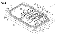
- Fig. 2 is a perspective view showing a state in which the capacitor substrate 60 on which capacitors 61 are arranged and mounted is removed from the inverter device shown in Fig. 1 .
- An inverter device 1 is a so-called three-phase inverter that outputs a three-phase (u/v/w phases) alternating current, and drives a cargo handling motor and a traction motor of a forklift, for example.
- the inverter device 1 mainly includes a heat sink 10, a metal substrate 20 on which the MOS (Metal-Oxide-Semiconductor) transistors 21 are mounted, a substrate spacing member 30, spacer members 41, electrodes (components) 51, and the capacitor substrate 60 on which the capacitors 61 are mounted.
- MOS Metal-Oxide-Semiconductor
- the heat sink 10 is a member which lowers temperature by a diffusion action of heat generated in power conversion, and the metal substrate 20 is placed thereon.
- the heat transmitted to the heat sink 10 from the MOS transistors 21 and the like mounted on the metal substrate 20 is diffused from fins or the like formed on the surface of the heat sink.
- metal such as aluminum, copper, or the like with high thermal conductivity is used.
- Through holes 27 and 67 (refer to Fig. 3A and Fig. 4 ) of the metal substrate 20 and the capacitor substrate 60, and screw holes 17 into which screws 43 to be inserted into the spacer members 41 are screwed are formed in the vicinity of the circumferential edge portions of the heat sink 10.
- the MOS transistors 21 are mounted on the metal substrate 20.
- transistor groups 21u, 21v, and 21w are respectively formed for the u phase, the v phase, and the w phase.
- the MOS transistors 21 and the electrodes 51 are disposed in consideration of low-inductance, electric current balance, and the like.
- the through holes 27 into which the screws 43 which will be described later are inserted are formed in a circumferential edge portion 20a of the metal substrate 20.
- the spacer members 41 are members for keeping a space between the metal substrate 20 and the capacitor substrate 60 at a predetermined spacing.
- the spacer members 41 are disposed in the vicinity of the circumferential edge portions 20a and 60a of the metal substrate 20 and the capacitor substrate 60.
- the spacer members 41 have through holes 41a into which the screws 43 for fastening the metal substrate 20 and the capacitor substrate 60 to the heat sink 10 are inserted.
- the substrate spacing member 30 is a member for positioning and holding the spacer members 41 at predetermined positions at the time of tightening the spacer members 41 to be sandwiched between the metal substrate 20 and the capacitor substrate 60 together. Further, the substrate spacing member 30 has a function of positioning and holding the electrodes 51 serving as components disposed between the both substrates at predetermined positions.
- the substrate spacing member 30 is formed of an insulating member. As an insulating member, for example, resin, ceramic, or the like is used.
- the substrate spacing member 30 has spacer member holding portions 31, a frame body portion 33, branch portions 35, and electrode holding portions (branch holding portions) 37.
- the spacer member holding portions 31 are portions for holding the spacer members 41. A plurality of the spacer member holding portions 31 are formed. In the substrate spacing member 30 of the present embodiment, the spacer member holding portions 31 are formed by two pairs of three, that is, six in total, along the long side direction. The spacer member holding portions 31 are formed according to the number and the layout positions of the spacer members 41 which are appropriately determined in consideration of the sizes and the like of the metal substrate 20 and the capacitor substrate 60.
- the frame body portion 33 is a portion which connects the plurality of spacer member holding portions 31 together, and is formed into a frame form along the circumferential edge portions 20a and 60a of the metal substrate 20 and the capacitor substrate 60.
- the branch portions 35 are portions which extend from the frame body portion 33 or the spacer member holding portions 31 up to the above-described predetermined positions when the spacer members 41 are held by the spacer member holding portions 31.
- the two branch portions 35 are formed.
- One of the branch portions 35 is formed so as to extend from the spacer member holding portion 31 up to an attaching position of the electrode 51 between the metal substrate 20 and the capacitor substrate 60.
- the other branch portions 35 are formed so as to extend from the frame body portion 33 up to an attaching position of the electrode 51 between the metal substrate 20 and the capacitor substrate 60.
- the electrode holding portions 37 are portions which are provided at the tip ends of the branch portions 35, and hold the electrodes 51 at the attaching positions of the electrodes 51 between the metal substrate 20 and the capacitor substrate 60.
- the two electrode holding portions 37 are provided. The electrodes 51 are inserted into the electrode holding portions 37.
- the electrodes 51 form electric pathways between the metal substrate 20 and the capacitor substrate 60.
- the electrodes 51 are formed of current-carrying materials. Examples of the current-carrying materials include aluminum, brass, and the like. Further, plate processing may be applied to the electrodes 51. Positions (attaching positions) at which the electrodes 51 are disposed between the metal substrate 20 and the capacitor substrate 60 are determined in consideration of inductance, electric current balance, and the like of the inverter device 1. According to downsizing of the inverter device 1, the electrodes 51 are disposed in the central portions of the transistor groups composed of the plurality of MOS transistors 21 1 which are connected sequentially.
- the capacitors 61 are mounted on the capacitor substrate 60.
- the through holes 67 into which the spacer members 41 are inserted are formed in the vicinity of the circumferential edge portion 60a of the capacitor substrate 60.
- the metal substrate 20 and the capacitor substrate 60 are fastened to the heat sink 10 with the screws 43 so as to be at a predetermined spacing with the spacer members 41.
- the screws 43 are inserted into the through holes 67, the spacer members 41, and the through holes 27.
- the screws 43 are inserted from the side of the capacitor substrate 60, to be screwed into the screw holes 17 of the heat sink 10.
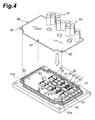
- Figs. 3A and 3B , and Fig. 4 are diagrams showing an embodiment of an assembling method of the inverter device 1.
- the metal substrate 20 is placed on the heat sink 10. At this time, alignment is performed such that the positions of the screw holes 17 of the heat sink 10 and the positions of the through holes 27 of the metal substrate 20 are matched to one another.
- the electrodes 51 are inserted into the electrode holding portions 37, and further, the substrate spacing member 30 in which the spacer members 41 are held by the spacer member holding portions 31 is prepared. Then, the substrate spacing member 30 holding the spacer members 41 and the electrodes 51 is placed on the metal substrate 20 (refer to Fig. 3B ). At this time, alignment is performed such that the positions of the through holes 41a of the spacer members 41 and the positions of the through holes 27 of the metal substrate are matched to one another.
- This substrate spacing member 30 is formed such that the electrode holding portions 37 are disposed on the above-described predetermined positions when the substrate spacing member 30 is placed on the metal substrate 20 such that the spacer member holding portions 31 are matched to the layout positions of the spacer members 41 on the metal substrate 20, i.e., the layout positions of the through holes 27 of the metal substrate 20. Therefore, provided that the substrate spacing member 30 in a state in which the electrodes 51 are held by the electrode holding portions 37 is prepared, and is mounted such that the positions of the spacer member holding portions 31 of the substrate spacing member 30 are matched to the through holes 27 on the metal substrate 20, the electrodes 51 are positioned and held at desired positions intended to be fixed between the metal substrate 20 and the capacitor substrate 60.
- the capacitor substrate 60 is mounted on the metal substrate 20 in which the electrodes 51 are positioned and held by the substrate spacing member 30. At this time, alignment is performed such that the positions of the through holes 67 of the capacitor substrate 60 and the positions of the through holes 41a of the spacer members 41 are matched to one another.
- the screws 43 are inserted into the through holes 67 of the capacitor substrate 60, the through holes 41a of the spacer members 41, and the through holes 27 of the metal substrate 20, to be screwed into the screw holes 17 provided in the heat sink 10. Accordingly, the electrodes 51 and the spacer members 41 are tightened together by the metal substrate 20 and the capacitor substrate 60. Then, components such as an input terminal which are not shown in the drawings are attached, which completes the inverter device 1 as shown in Fig. 1 .
- the substrate spacing member 30 of the above-described embodiment is formed such that the electrode holding portions 37 are capable of holding the electrodes 51 which are rectangular in planar view.
- the electrodes 51 have been described as an example of components which are positioned and held by the substrate spacing member 30.
- the present invention is not limited to this example.
- capacitors, resistors, switching elements, substrates, wiring busbars, heat radiating sheets, and the like may serve as components composing electric equipment such as an inverter.
- the substrate spacing member 30 of the above-described embodiment has been described by use of the example in which the spacer member holding portions 31 and the spacer members 41 are respectively configured as separate components.
- the present invention is not limited to this example, and the spacer member holding portions 31 and the spacer members 41 may be configured as one member (a spacer portion).
- the substrate spacing member 30 of the above-described embodiment has been described by use of the example of the branch portions 35 of a shape extending from the spacer member holding portions 31 or the frame body portion 33 up to the attaching position of the electrodes 51 as shown in Fig. 2 .
- the present invention is not limited this example.
- the branch holding portion 37 may have a first branch holding portion 37a which holds the component 51 at the predetermined position, and a second branch holding portion 37b which holds a component 152 around the first branch holding portion 37a.
- the branch holding portion 37 may have a second branch holding portion 37c which extends toward the adjacent branch holding portion 37, and holds a component 151 around the first branch holding portion 37a.
- the adjacent branch holding portion 37 has the second branch holding portion 37c with the same configuration, thereby, it is possible to hold the component 151 around the first branch holding portion 37a.
- Fig. 5 shows the example in which the second branch holding portions 37c adjacent to one another are integrally formed. However, it may be a configuration in which those are spaced from each other.
- the second branch holding portions 37b and 37c extending from the first branch holding portion 37a may be integrated with the first branch holding portion 37a, or may be separated from the first branch holding portion 37a.
- the substrate spacing member 30 it is possible to position and hold the components 151 and 152 disposed around the first branch holding portion 37a. Therefore, there is no need to provide a new branch portion and branch holding portion for holding there components 151 and 152.
- the frame body portion 33 may be formed into a frame form along the circumferential edge portions of the metal substrate (substrate) 20 and the capacitor substrate (substrate) 60, and the substrate spacing member 30 may further include a frame body holding portion 131 which is provided at the frame body portion 33, and holds a component 153 (155, 157).
- the substrate spacing member 30 it is possible to position and hold the components 153 (155, 157) at the circumferential edge portions of the metal substrate 20 and the capacitor substrate 60 as well. Therefore, it is possible to improve the degree of freedom of layout of the components.
- the frame body holding portion 131 may have a first frame body holding portion 131a which holds the component 155 at a predetermined position, and a second frame body holding portion 131b which holds a component 156 around the first frame body holding portion 131a.
- the frame body holding portion 131 which holds the component 155 may have a second frame body holding portion 131c which extends toward the adjacent frame body holding portion 131, and holds a component 159 around the first frame body holding portion 131a.
- the adjacent frame body holding portion 131 has the second frame body holding portion 131c with the same configuration, thereby, it is possible to hold the component 159 around the first frame body holding portion 131a.
- Fig. 5 shows the example in which the second frame body holding portions 131c adjacent to one another are integrally formed. However, it may be a configuration in which those are spaced from each other.
- the second frame body holding portions 131b and 131c extending from the first frame body holding portion 131a may be integrated with the first frame body holding portion 131a, or may be separated from the first frame body holding portion 131a.
- the substrate spacing member 30 it is possible to position and hold the components 156 and 159 disposed around the first frame body holding portion 131a. Therefore, there is no need to provide a new frame body holding portion 131 for holding there components 156 and 159.
- the branch holding portion 37 may have the second branch holding portion 37c which extends toward the adjacent frame body holding portion 131, and holds a component 161 around the first branch holding portion 37a.
- the adjacent frame body holding portion 131 has the second frame body holding portion 131c with the same configuration, thereby, it is possible to hold the component 161 around the first branch holding portion 37a.
- Fig. 5 shows the example in which the second branch holding portion 37c and the second frame body holding portion 131c adjacent to one another are integrally formed. However, it may be a configuration in which those are spaced from each other.
- the second branch holding portion 37c extending from the first branch holding portion 37a may be integrated with the first branch holding portion 37a, or may be separated from the first branch holding portion 37a.
- the second frame body holding portion 131c extending from the first frame body holding portion 131a may be integrated with, or may be separated from the first frame body holding portion 131a.
- the branch portions 35 may be provided so as to connect the spacer member holding portions 31 or the frame body portion 33 provided on one of the long sides and the spacer member holding portions 31 or the frame body portion 33 provided at the opposite position.
- the branch portions 35 may be formed in a grid pattern. Accordingly, it is possible to improve the accuracy of position at the time of positioning and holding the components 51 at predetermined positions on the metal substrate 20.
- the substrate spacing member 30 may include a connection portion 45 for directly connecting the frame body portion 33 and the frame body portion 33. Accordingly, it is possible to maintain the shape of the substrate spacing member 30, and it is possible to position and hold a target component at a more precise position.
- the inverter device 1 of the above-described embodiment has been described by use of the example in which the screws 43 are inserted into the through holes 67 of the capacitor substrate 60, the through holes 41a of the spacer members 41, and the through holes 27 of the metal substrate 20 from the capacitor substrate 60 side, to be screwed into the screw holes 17 provided in the heat sink 10, thereby tightening the electrodes 51 and the spacer members 41 together by the metal substrate 20 and the capacitor substrate 60.
- through holes may be respectively provided at positions of the metal substrate 20 and the capacitor substrate 60 which correspond to the position at which the electrodes 51 are disposed, through holes may be provided in the electrodes 51, and screw holes may be provided at positions of the heat sink 10 which correspond to the positions. Accordingly, because the screws are able to be inserted into the through holes of the capacitor substrate, the through holes of the electrodes, and the through holes of the metal substrate from the capacitor substrate 60 side, to be screwed into the screw holes in the heat sink, it is possible to tighten the electrodes 51 and the spacer members 41 together by the metal substrate 20 and the capacitor substrate 60.
- a configuration in which a screw groove may be provided in the edge portion of the spacer member 41, so as to be able to screwed into the screw hole 17 provided in the heat sink 10 may be adopted, or a fit-in portion to be fit into the screw hole 17 may be provided at the edge portion of the spacer member 41.
- claw portions for positioning the substrate spacing member 30 at a predetermined position on the metal substrate 20 may be provided at the spacer member holding portions 31 and the frame body portion 33, or the like. Even in such a case, it is possible to improve the accuracy of position at the time of positioning and holding the electrodes 51 on the metal substrate 20.
- the spacer member 41 and the electrode 51 are respectively inserted into (pressed into) the spacer member holding portion 31 and the electrode holding portion 37 has been described.
- the spacer member 41 and the spacer member holding portion 31 may be integrally formed, or the electrode 51 and the electrode holding portion 37 may be integrally formed.
- the substrate spacing member 30 of the above-described embodiment has been described by use of the example in which the electrode holding portions 37 are formed so as to be capable of holding the electrodes 51 which are rectangular in planar view. However, it is not limited to this example.
- the holding portions 37 may be formed so as to be capable of holding the electrodes 51 which are circular, oval, or polygonal in planar view.
- the thicknesses in the laminating direction of the both substrates 20 and 60 in the spacer member holding portions 31, the frame body portion 33, the branch portions 35, and the electrode holding portions 37 may be shorter than the spacer members 41 and the electrodes 51. That is, there is no need to have a function of keeping a distance between the metal substrate 20 and the capacitor substrate 60 constant.
- a substrate spacing member includes a spacer portion which is disposed between the two substrates in contact with both edge portions thereof to keep a distance between the two substrates constant" spacer member holding portions which hold the spacer members, a frame body portion that connects the spacer member holding portions to each other, a branch portion which extends toward a predetermined position between the two substrates from the frame body portion or the spacer member holding portions, and electrode holding portions which are provided at the branch portions, and hold electrodes at the predetermined positions.
Landscapes
- Engineering & Computer Science (AREA)
- Microelectronics & Electronic Packaging (AREA)
- Inverter Devices (AREA)
- Cooling Or The Like Of Electrical Apparatus (AREA)
- Combinations Of Printed Boards (AREA)
- Coils Of Transformers For General Uses (AREA)
- Insulating Of Coils (AREA)
Abstract
Description
- The present invention relates to a substrate spacing member for keeping a space between two substrates, and has an electronic component positioning function, and an inverter device.
- As a method for temporarily fixing (positioning and holding) electronic components such as ICs, capacitors, and electrodes at predetermined positions on a substrate, a method using a fixture tool has been generally known. For example, as a method for temporarily fixing a plurality of electronic components at predetermined positions, Patent Literature 1 (Japanese Patent Application Laid-Open No.
2002-344199 Patent Literature 1, a fixture tool having a housing portion in which a plurality of electronic components are collectively housed is prepared, and the electronic components are temporarily fixed by pressing the fixture tool against the substrate side while a plurality of electronic components mounted on a predetermined position on a substrate are housed in the housing portion of the fixture tool (refer to Patent Literature 1). - However, for example, in a compact inverter device in which a plurality of electronic components are disposed between two substrates held at a predetermined spacing, it is difficult to temporarily fix the electronic components to be disposed between the substrates by use of a pressing-type fixture tool having a housing portion as in the
Patent Literature 1. That is, because a space between the substrates becomes narrow according to downsizing of an inverter, and other electronic components are further disposed around the electronic components disposed between the substrates, it is impossible to secure an area from and to which a pressing type fixture tool having a component housing portion is detached and attached. Therefore, a method for temporarily fixing the electronic components on one of the substrates by soldering in advance, and thereafter, disposing the other substrate so as to sandwich the temporarily-fixed electronic components therebetween may be considered. However, the number of processes for solder-joining the electronic components is increased, which causes another problem of increasing the manufacturing cost of the inverter device. - Therefore, an object of the present invention is to provide a substrate spacing member which is capable of easily positioning and holding components to be disposed between two substrates which are held at a predetermined spacing, and an inverter device.
- A substrate spacing member according to an aspect of the present invention which is disposed between two substrates on which electronic components are mounted, and keeps a distance between the two substrates constant, the substrate spacing member includes a spacer portion which is disposed between the two substrates in contact with both edge portions thereof to keep a distance between the two substrates constant, a frame body portion that connects the spacer portions together, a branch portion which extends toward a predetermined position between the two substrates from the frame body portion or the spacer portion, and a branch holding portion which is provided at the branch portion, and holds a component at the predetermined position.
- According to this substrate spacing member, positioning of the component with respect to the substrates is completed by only inserting a component into the branch holding portion, and disposing the spacer portion for keeping a space between the two substrates at the predetermined position. Thereby, it is possible to easily position the component at the predetermined position even without use of soldering or a tool.
- In addition, the term "components" here includes capacitors, resistors, switching elements, substrates, electrodes, wiring busbars, heat radiating sheets, and the like serving as components composing electric equipment such as an inverter.
- The branch holding portion may have a first branch holding portion which holds the component at the predetermined position, and a second branch holding portion which holds a component around the first branch holding portion.
- According to this substrate spacing member, it is possible to temporarily fix components which are disposed around the first branch holding portion by the second branch holding portion provided adjacent to the first branch holding portion.
- The frame body portion is formed into a frame form along circumferential edge portions of the substrates, and the substrate spacing member may further have a frame body holding portion which is provided at the frame body portion, and holds the component.
- According to this substrate spacing member, because it is possible to temporarily fix components to the circumferential edge portions of the substrates, it is possible to improve the degree of freedom of layout of the components.
- The frame body holding portion may have a first frame body holding portion which holds the component, and a second frame body holding portion which holds a component around the first frame body holding portion.
- According to this substrate spacing member, it is possible to temporarily fix components to be disposed around the first frame body holding portion by the second frame body holding portion which is provided adjacent to the first frame body holding portion.
- The spacer portion has a spacer member and a spacer member holding portion which holds the spacer member, and the spacer member held by the spacer member holding portion has conductive properties, and includes a through hole into which a screw is able to be inserted, and the spacer member holding portion may be formed of an insulating body.
- According to this substrate spacing member, it is possible to ground the other substrate via the spacer member by grounding one of the substrates. Further, it is possible to easily fix the two substrates on a heat sink by inserting a screw into the through hole of the spacer member.
- An inverter device according to an aspect of the present invention includes a heat sink, a metal substrate which is placed on the heat sink, and on which switching elements are mounted, a capacitor substrate which is disposed so as to face the metal substrate, and on which capacitors are mounted, an electrode which is disposed between the metal substrate and the capacitor substrate, and which electrically connects the metal substrate and the capacitor substrate, and the above-described substrate spacing member, the inverter device in which the electrode is held by the branch holding portion included in the substrate spacing member.
- According to the present invention, it is possible to easily position and hold (temporarily fix) a component to be disposed between the two substrates which are held at a predetermined spacing.
-
-
Fig. 1 is a perspective view showing an inverter device including a substrate spacing member according to an embodiment. -
Fig. 2 is a perspective view showing a state in which a capacitor substrate on which capacitors are disposed is removed from the inverter device shown inFig. 1 . -
Figs. 3A and 3B are drawings showing an embodiment of an assembling method of the inverter device. -
Fig. 4 is a drawing showing an embodiment of an assembling method of the inverter device. -
Fig. 5 is a perspective view showing a substrate spacing member according to another embodiment. -
Fig. 6 is a perspective view showing a substrate spacing member according to yet another embodiment. - Hereinafter, an embodiment will be described in detail with reference to the drawings. In addition, the same or corresponding portions in the respective drawings are shown with the same symbols. The dimensional ratios in the drawings are not necessarily proportional to those in the description. In the description, the words referring to directions such as "upper" and "lower" are expedient words based on the states shown in the drawings.
-
Fig. 1 is a perspective view showing an inverter device including a substrate spacing member according to an embodiment. InFig. 1 , in order to show the layout state ofMOS transistors 21 and the like which are disposed under acapacitor substrate 60, thecapacitor substrate 60 is shown in a transparent state.Fig. 2 is a perspective view showing a state in which thecapacitor substrate 60 on whichcapacitors 61 are arranged and mounted is removed from the inverter device shown inFig. 1 . - An
inverter device 1 is a so-called three-phase inverter that outputs a three-phase (u/v/w phases) alternating current, and drives a cargo handling motor and a traction motor of a forklift, for example. Theinverter device 1 mainly includes aheat sink 10, ametal substrate 20 on which the MOS (Metal-Oxide-Semiconductor)transistors 21 are mounted, asubstrate spacing member 30,spacer members 41, electrodes (components) 51, and thecapacitor substrate 60 on which thecapacitors 61 are mounted. - The
heat sink 10 is a member which lowers temperature by a diffusion action of heat generated in power conversion, and themetal substrate 20 is placed thereon. The heat transmitted to theheat sink 10 from theMOS transistors 21 and the like mounted on themetal substrate 20 is diffused from fins or the like formed on the surface of the heat sink. For theheat sink 10, metal such as aluminum, copper, or the like with high thermal conductivity is used. Throughholes 27 and 67 (refer toFig. 3A andFig. 4 ) of themetal substrate 20 and thecapacitor substrate 60, and screwholes 17 into whichscrews 43 to be inserted into thespacer members 41 are screwed are formed in the vicinity of the circumferential edge portions of theheat sink 10. - As switching elements, for example, the
MOS transistors 21 are mounted on themetal substrate 20. In theMOS transistors 21,transistor groups MOS transistors 21 and theelectrodes 51 are disposed in consideration of low-inductance, electric current balance, and the like. The throughholes 27 into which thescrews 43 which will be described later are inserted are formed in acircumferential edge portion 20a of themetal substrate 20. - The
spacer members 41 are members for keeping a space between themetal substrate 20 and thecapacitor substrate 60 at a predetermined spacing. Thespacer members 41 are disposed in the vicinity of thecircumferential edge portions metal substrate 20 and thecapacitor substrate 60. Thespacer members 41 have throughholes 41a into which thescrews 43 for fastening themetal substrate 20 and thecapacitor substrate 60 to theheat sink 10 are inserted. - The
substrate spacing member 30 is a member for positioning and holding thespacer members 41 at predetermined positions at the time of tightening thespacer members 41 to be sandwiched between themetal substrate 20 and thecapacitor substrate 60 together. Further, thesubstrate spacing member 30 has a function of positioning and holding theelectrodes 51 serving as components disposed between the both substrates at predetermined positions. Thesubstrate spacing member 30 is formed of an insulating member. As an insulating member, for example, resin, ceramic, or the like is used. Thesubstrate spacing member 30 has spacermember holding portions 31, aframe body portion 33,branch portions 35, and electrode holding portions (branch holding portions) 37. - The spacer
member holding portions 31 are portions for holding thespacer members 41. A plurality of the spacermember holding portions 31 are formed. In thesubstrate spacing member 30 of the present embodiment, the spacermember holding portions 31 are formed by two pairs of three, that is, six in total, along the long side direction. The spacermember holding portions 31 are formed according to the number and the layout positions of thespacer members 41 which are appropriately determined in consideration of the sizes and the like of themetal substrate 20 and thecapacitor substrate 60. - The
frame body portion 33 is a portion which connects the plurality of spacermember holding portions 31 together, and is formed into a frame form along thecircumferential edge portions metal substrate 20 and thecapacitor substrate 60. - The
branch portions 35 are portions which extend from theframe body portion 33 or the spacermember holding portions 31 up to the above-described predetermined positions when thespacer members 41 are held by the spacermember holding portions 31. In thesubstrate spacing member 30 of the present embodiment, the twobranch portions 35 are formed. One of thebranch portions 35 is formed so as to extend from the spacermember holding portion 31 up to an attaching position of theelectrode 51 between themetal substrate 20 and thecapacitor substrate 60. Theother branch portions 35 are formed so as to extend from theframe body portion 33 up to an attaching position of theelectrode 51 between themetal substrate 20 and thecapacitor substrate 60. - The
electrode holding portions 37 are portions which are provided at the tip ends of thebranch portions 35, and hold theelectrodes 51 at the attaching positions of theelectrodes 51 between themetal substrate 20 and thecapacitor substrate 60. In thesubstrate spacing member 30 of the present embodiment, the twoelectrode holding portions 37 are provided. Theelectrodes 51 are inserted into theelectrode holding portions 37. - The
electrodes 51 form electric pathways between themetal substrate 20 and thecapacitor substrate 60. Theelectrodes 51 are formed of current-carrying materials. Examples of the current-carrying materials include aluminum, brass, and the like. Further, plate processing may be applied to theelectrodes 51. Positions (attaching positions) at which theelectrodes 51 are disposed between themetal substrate 20 and thecapacitor substrate 60 are determined in consideration of inductance, electric current balance, and the like of theinverter device 1. According to downsizing of theinverter device 1, theelectrodes 51 are disposed in the central portions of the transistor groups composed of the plurality ofMOS transistors 21 1 which are connected sequentially. - The
capacitors 61 are mounted on thecapacitor substrate 60. The through holes 67 into which thespacer members 41 are inserted are formed in the vicinity of thecircumferential edge portion 60a of thecapacitor substrate 60. - The
metal substrate 20 and thecapacitor substrate 60 are fastened to theheat sink 10 with thescrews 43 so as to be at a predetermined spacing with thespacer members 41. Thescrews 43 are inserted into the throughholes 67, thespacer members 41, and the through holes 27. Thescrews 43 are inserted from the side of thecapacitor substrate 60, to be screwed into the screw holes 17 of theheat sink 10. - Next, an assembling method of the
inverter device 1 will be described by use ofFigs. 3A and 3B , andFig. 4 .Figs. 3A and 3B , andFig. 4 are diagrams showing an embodiment of an assembling method of theinverter device 1. - First, as shown in
Fig. 3A , themetal substrate 20 is placed on theheat sink 10. At this time, alignment is performed such that the positions of the screw holes 17 of theheat sink 10 and the positions of the throughholes 27 of themetal substrate 20 are matched to one another. - Next, the
electrodes 51 are inserted into theelectrode holding portions 37, and further, thesubstrate spacing member 30 in which thespacer members 41 are held by the spacermember holding portions 31 is prepared. Then, thesubstrate spacing member 30 holding thespacer members 41 and theelectrodes 51 is placed on the metal substrate 20 (refer toFig. 3B ). At this time, alignment is performed such that the positions of the throughholes 41a of thespacer members 41 and the positions of the throughholes 27 of the metal substrate are matched to one another. - This
substrate spacing member 30 is formed such that theelectrode holding portions 37 are disposed on the above-described predetermined positions when thesubstrate spacing member 30 is placed on themetal substrate 20 such that the spacermember holding portions 31 are matched to the layout positions of thespacer members 41 on themetal substrate 20, i.e., the layout positions of the throughholes 27 of themetal substrate 20. Therefore, provided that thesubstrate spacing member 30 in a state in which theelectrodes 51 are held by theelectrode holding portions 37 is prepared, and is mounted such that the positions of the spacermember holding portions 31 of thesubstrate spacing member 30 are matched to the throughholes 27 on themetal substrate 20, theelectrodes 51 are positioned and held at desired positions intended to be fixed between themetal substrate 20 and thecapacitor substrate 60. - Next, as shown in
Fig. 4 , thecapacitor substrate 60 is mounted on themetal substrate 20 in which theelectrodes 51 are positioned and held by thesubstrate spacing member 30. At this time, alignment is performed such that the positions of the throughholes 67 of thecapacitor substrate 60 and the positions of the throughholes 41a of thespacer members 41 are matched to one another. - Next, the
screws 43 are inserted into the throughholes 67 of thecapacitor substrate 60, the throughholes 41a of thespacer members 41, and the throughholes 27 of themetal substrate 20, to be screwed into the screw holes 17 provided in theheat sink 10. Accordingly, theelectrodes 51 and thespacer members 41 are tightened together by themetal substrate 20 and thecapacitor substrate 60. Then, components such as an input terminal which are not shown in the drawings are attached, which completes theinverter device 1 as shown inFig. 1 . - The
substrate spacing member 30 of the above-described embodiment is formed such that theelectrode holding portions 37 are capable of holding theelectrodes 51 which are rectangular in planar view. - Although one embodiment has been described above, the present invention is not limited to the above-described embodiment, and various modifications are possible within the scope without departing from the spirit of the invention.
- In the above embodiment, the
electrodes 51 have been described as an example of components which are positioned and held by thesubstrate spacing member 30. However, the present invention is not limited to this example. For example, capacitors, resistors, switching elements, substrates, wiring busbars, heat radiating sheets, and the like may serve as components composing electric equipment such as an inverter. - The
substrate spacing member 30 of the above-described embodiment has been described by use of the example in which the spacermember holding portions 31 and thespacer members 41 are respectively configured as separate components. However, the present invention is not limited to this example, and the spacermember holding portions 31 and thespacer members 41 may be configured as one member (a spacer portion). - The
substrate spacing member 30 of the above-described embodiment has been described by use of the example of thebranch portions 35 of a shape extending from the spacermember holding portions 31 or theframe body portion 33 up to the attaching position of theelectrodes 51 as shown inFig. 2 . However, the present invention is not limited this example. - For example, as shown in
Fig. 5 , thebranch holding portion 37 may have a firstbranch holding portion 37a which holds thecomponent 51 at the predetermined position, and a secondbranch holding portion 37b which holds acomponent 152 around the firstbranch holding portion 37a. - Further, for example, as shown in
Fig. 5 , thebranch holding portion 37 may have a secondbranch holding portion 37c which extends toward the adjacentbranch holding portion 37, and holds acomponent 151 around the firstbranch holding portion 37a. Here, the adjacentbranch holding portion 37 has the secondbranch holding portion 37c with the same configuration, thereby, it is possible to hold thecomponent 151 around the firstbranch holding portion 37a. In addition,Fig. 5 shows the example in which the secondbranch holding portions 37c adjacent to one another are integrally formed. However, it may be a configuration in which those are spaced from each other. - The second
branch holding portions branch holding portion 37a may be integrated with the firstbranch holding portion 37a, or may be separated from the firstbranch holding portion 37a. - According to this configuration of the
substrate spacing member 30, it is possible to position and hold thecomponents branch holding portion 37a. Therefore, there is no need to provide a new branch portion and branch holding portion for holding therecomponents - Further, for example, as shown in
Fig. 5 , theframe body portion 33 may be formed into a frame form along the circumferential edge portions of the metal substrate (substrate) 20 and the capacitor substrate (substrate) 60, and thesubstrate spacing member 30 may further include a framebody holding portion 131 which is provided at theframe body portion 33, and holds a component 153 (155, 157). According to this configuration of thesubstrate spacing member 30, it is possible to position and hold the components 153 (155, 157) at the circumferential edge portions of themetal substrate 20 and thecapacitor substrate 60 as well. Therefore, it is possible to improve the degree of freedom of layout of the components. - Further, for example, as shown in
Fig. 5 , the framebody holding portion 131 may have a first framebody holding portion 131a which holds thecomponent 155 at a predetermined position, and a second framebody holding portion 131b which holds acomponent 156 around the first framebody holding portion 131a. - Further, for example, as shown in
Fig. 5 , the framebody holding portion 131 which holds thecomponent 155 may have a second framebody holding portion 131c which extends toward the adjacent framebody holding portion 131, and holds acomponent 159 around the first framebody holding portion 131a. Here, the adjacent framebody holding portion 131 has the second framebody holding portion 131c with the same configuration, thereby, it is possible to hold thecomponent 159 around the first framebody holding portion 131a. In addition,Fig. 5 shows the example in which the second framebody holding portions 131c adjacent to one another are integrally formed. However, it may be a configuration in which those are spaced from each other. - The second frame
body holding portions body holding portion 131a may be integrated with the first framebody holding portion 131a, or may be separated from the first framebody holding portion 131a. - According to this configuration of the
substrate spacing member 30, it is possible to position and hold thecomponents body holding portion 131a. Therefore, there is no need to provide a new framebody holding portion 131 for holding therecomponents - Moreover, for example, as shown in
Fig. 5 , thebranch holding portion 37 may have the secondbranch holding portion 37c which extends toward the adjacent framebody holding portion 131, and holds acomponent 161 around the firstbranch holding portion 37a. Here, the adjacent framebody holding portion 131 has the second framebody holding portion 131c with the same configuration, thereby, it is possible to hold thecomponent 161 around the firstbranch holding portion 37a. In addition,Fig. 5 shows the example in which the secondbranch holding portion 37c and the second framebody holding portion 131c adjacent to one another are integrally formed. However, it may be a configuration in which those are spaced from each other. - The second
branch holding portion 37c extending from the firstbranch holding portion 37a may be integrated with the firstbranch holding portion 37a, or may be separated from the firstbranch holding portion 37a. The second framebody holding portion 131c extending from the first framebody holding portion 131a may be integrated with, or may be separated from the first framebody holding portion 131a. - According to this configuration of the
substrate spacing member 30, it is possible to position and hold thecomponent 161 disposed around the firstbranch holding portion 37a. Therefore, there is no need to provide the newbranch holding portion 37 for holding thiscomponent 161. - Further, for example, as shown in
Figs. 5 and6 , thebranch portions 35 may be provided so as to connect the spacermember holding portions 31 or theframe body portion 33 provided on one of the long sides and the spacermember holding portions 31 or theframe body portion 33 provided at the opposite position. In other words, thebranch portions 35 may be formed in a grid pattern. Accordingly, it is possible to improve the accuracy of position at the time of positioning and holding thecomponents 51 at predetermined positions on themetal substrate 20. - Moreover, as shown in
Fig. 6 , thesubstrate spacing member 30 may include aconnection portion 45 for directly connecting theframe body portion 33 and theframe body portion 33. Accordingly, it is possible to maintain the shape of thesubstrate spacing member 30, and it is possible to position and hold a target component at a more precise position. - The
inverter device 1 of the above-described embodiment has been described by use of the example in which thescrews 43 are inserted into the throughholes 67 of thecapacitor substrate 60, the throughholes 41a of thespacer members 41, and the throughholes 27 of themetal substrate 20 from thecapacitor substrate 60 side, to be screwed into the screw holes 17 provided in theheat sink 10, thereby tightening theelectrodes 51 and thespacer members 41 together by themetal substrate 20 and thecapacitor substrate 60. However, it is not limited to this example. - For example, through holes may be respectively provided at positions of the
metal substrate 20 and thecapacitor substrate 60 which correspond to the position at which theelectrodes 51 are disposed, through holes may be provided in theelectrodes 51, and screw holes may be provided at positions of theheat sink 10 which correspond to the positions. Accordingly, because the screws are able to be inserted into the through holes of the capacitor substrate, the through holes of the electrodes, and the through holes of the metal substrate from thecapacitor substrate 60 side, to be screwed into the screw holes in the heat sink, it is possible to tighten theelectrodes 51 and thespacer members 41 together by themetal substrate 20 and thecapacitor substrate 60. - Further, with the configuration in which it is possible to fix the
spacer members 41 to theheat sink 10, it is possible to fix thespacer members 41 in a state in which themetal substrate 20 is mounted on theheat sink 10, and dispose thesubstrate spacing member 30 so as to hold thespacer members 41. In this way, it is possible to improve the accuracy of position at the time of positioning and holding theelectrodes 51 between themetal substrate 20 and thecapacitor substrate 60. In addition, as a configuration in which thespacer members 41 are fixed to theheat sink 10, a configuration in which a screw groove may be provided in the edge portion of thespacer member 41, so as to be able to screwed into thescrew hole 17 provided in theheat sink 10 may be adopted, or a fit-in portion to be fit into thescrew hole 17 may be provided at the edge portion of thespacer member 41. - Further, claw portions for positioning the
substrate spacing member 30 at a predetermined position on themetal substrate 20 may be provided at the spacermember holding portions 31 and theframe body portion 33, or the like. Even in such a case, it is possible to improve the accuracy of position at the time of positioning and holding theelectrodes 51 on themetal substrate 20. - In the above-described embodiment, the example in which the
spacer member 41 and theelectrode 51 are respectively inserted into (pressed into) the spacermember holding portion 31 and theelectrode holding portion 37 has been described. However, thespacer member 41 and the spacermember holding portion 31 may be integrally formed, or theelectrode 51 and theelectrode holding portion 37 may be integrally formed. - The
substrate spacing member 30 of the above-described embodiment has been described by use of the example in which theelectrode holding portions 37 are formed so as to be capable of holding theelectrodes 51 which are rectangular in planar view. However, it is not limited to this example. The holdingportions 37 may be formed so as to be capable of holding theelectrodes 51 which are circular, oval, or polygonal in planar view. - Further, the thicknesses in the laminating direction of the both
substrates member holding portions 31, theframe body portion 33, thebranch portions 35, and theelectrode holding portions 37 may be shorter than thespacer members 41 and theelectrodes 51. That is, there is no need to have a function of keeping a distance between themetal substrate 20 and thecapacitor substrate 60 constant. - A substrate spacing member includes a spacer portion which is disposed between the two substrates in contact with both edge portions thereof to keep a distance between the two substrates constant" spacer member holding portions which hold the spacer members, a frame body portion that connects the spacer member holding portions to each other, a branch portion which extends toward a predetermined position between the two substrates from the frame body portion or the spacer member holding portions, and electrode holding portions which are provided at the branch portions, and hold electrodes at the predetermined positions.
Claims (6)
- A substrate spacing member which is disposed between two substrates on which electronic components are mounted, and keeps a distance between the two substrates constant, the substrate spacing member comprising:a spacer portion which is disposed between the two substrates in contact with both edge portions thereof, to keep a distance between the two substrates constant;a frame body portion that connects the spacer portions together;a branch portion which extends toward a predetermined position between the two substrates from the frame body portion or the spacer portion; anda branch holding portion which is provided at the branch portion, and holds a component at the predetermined position.
- The substrate spacing member according to Claim 1, wherein the branch holding portion has a first branch holding portion which holds the component at the predetermined position, and a second branch holding portion which holds a component around the first branch holding portion.
- The substrate spacing member according to Claim 1 or Claim 2, wherein
the frame body portion is formed into a frame form along circumferential edge portions of the substrates, and
the substrate spacing member further has a frame body holding portion which is provided at the frame body portion, and holds the component. - The substrate spacing member according to Claim 3, wherein the frame body holding portion has a first frame body holding portion which holds the component, and a second frame body holding portion which holds a component around the first frame body holding portion.
- The substrate spacing member according to any one of Claims 1 to 4, wherein
the spacer portion has a spacer member and a spacer member holding portion which holds the spacer member, and the spacer member held by the spacer member holding portion has conductive properties, and includes a through hole into which a screw is able to be inserted, and
the spacer member holding portion is formed of an insulating body. - An inverter device comprising:a heat sink;a metal substrate which is mounted on the heat sink, and on which switching elements are mounted;a capacitor substrate which is disposed so as to face the metal substrate, and on which capacitors are mounted;an electrode which is disposed between the metal substrate and the capacitor substrate, and which electrically connects the metal substrate and the capacitor substrate; andthe substrate spacing member according to any one of Claims 1 to 5, the inverter device whereinthe electrode is held by the branch holding portion included in the substrate spacing member.
Applications Claiming Priority (1)
| Application Number | Priority Date | Filing Date | Title |
|---|---|---|---|
| JP2013058574A JP5803961B2 (en) | 2013-03-21 | 2013-03-21 | Substrate spacing member and inverter device |
Publications (3)
| Publication Number | Publication Date |
|---|---|
| EP2782432A2 true EP2782432A2 (en) | 2014-09-24 |
| EP2782432A3 EP2782432A3 (en) | 2017-02-01 |
| EP2782432B1 EP2782432B1 (en) | 2025-01-22 |
Family
ID=50272353
Family Applications (1)
| Application Number | Title | Priority Date | Filing Date |
|---|---|---|---|
| EP14158571.1A Active EP2782432B1 (en) | 2013-03-21 | 2014-03-10 | Substrate spacing member and inverter device |
Country Status (4)
| Country | Link |
|---|---|
| US (1) | US9485865B2 (en) |
| EP (1) | EP2782432B1 (en) |
| JP (1) | JP5803961B2 (en) |
| CN (1) | CN104066311B (en) |
Cited By (1)
| Publication number | Priority date | Publication date | Assignee | Title |
|---|---|---|---|---|
| WO2025162651A1 (en) * | 2024-01-31 | 2025-08-07 | Zf Friedrichshafen Ag | Frame for connecting to at least one printed circuit board and to a housing of an electronics module, system consisting of at least a printed circuit board and frame, and electric module |
Families Citing this family (3)
| Publication number | Priority date | Publication date | Assignee | Title |
|---|---|---|---|---|
| US11382223B2 (en) * | 2015-06-30 | 2022-07-05 | Lear Corporation | Spring and damper system and method for producing same |
| EP3522690B2 (en) * | 2018-02-02 | 2023-12-06 | Kabushiki Kaisha Toyota Jidoshokki | Inverter |
| DE102021110251B4 (en) | 2021-04-22 | 2024-12-19 | Sma Solar Technology Ag | Power semiconductor arrangement and inverter bridge with power semiconductor arrangement |
Citations (1)
| Publication number | Priority date | Publication date | Assignee | Title |
|---|---|---|---|---|
| JP2002344199A (en) | 2001-05-15 | 2002-11-29 | Hitachi Telecom Technol Ltd | Electronic component mounting jig |
Family Cites Families (17)
| Publication number | Priority date | Publication date | Assignee | Title |
|---|---|---|---|---|
| JPH0444190Y2 (en) * | 1986-06-10 | 1992-10-19 | ||
| US4908738A (en) * | 1986-12-19 | 1990-03-13 | Fanuc Ltd | Drive motor control unit |
| JPH03159192A (en) * | 1989-11-16 | 1991-07-09 | Sanyo Electric Co Ltd | Hybrid integrated circuit device |
| JPH073674Y2 (en) * | 1990-08-20 | 1995-01-30 | サンケン電気株式会社 | Electronic device |
| JP4262956B2 (en) * | 2002-10-09 | 2009-05-13 | 富士通テン株式会社 | How to connect printed circuit boards |
| EP1555864A1 (en) * | 2004-01-14 | 2005-07-20 | Thomson Licensing S.A. | RF circuit with stacked printed circuit boards |
| DE112005001446T5 (en) * | 2004-06-24 | 2007-05-31 | Kabushiki Kaisha Yaskawa Denki, Kitakyushu | motor control |
| US7248483B2 (en) * | 2004-08-19 | 2007-07-24 | Xantrex Technology, Inc. | High power density insulated metal substrate based power converter assembly with very low BUS impedance |
| JP4548619B2 (en) * | 2004-09-17 | 2010-09-22 | 株式会社安川電機 | Motor control device |
| DE102005044867B4 (en) * | 2005-09-20 | 2021-08-19 | Vitesco Technologies GmbH | Combined fastening and contacting system for electrical components on printed circuit boards arranged one above the other |
| CN101192443A (en) * | 2006-12-01 | 2008-06-04 | 宇瞻科技股份有限公司 | Extensible hard disk module |
| JP5041798B2 (en) * | 2006-12-15 | 2012-10-03 | 三菱電機株式会社 | Semiconductor device |
| JP5028085B2 (en) * | 2006-12-27 | 2012-09-19 | アイシン・エィ・ダブリュ株式会社 | Electronic circuit device and manufacturing method thereof |
| JP5409312B2 (en) * | 2009-01-30 | 2014-02-05 | キヤノン株式会社 | Multilayer printed circuit board |
| GB2487185B (en) * | 2011-01-05 | 2015-06-03 | Penny & Giles Controls Ltd | Power Switching Circuitry |
| CN202103950U (en) * | 2011-07-04 | 2012-01-04 | 深圳市日业电气有限公司 | Space connection structure for circuit board |
| DE102011054818A1 (en) * | 2011-10-26 | 2013-05-02 | Hella Kgaa Hueck & Co. | Electronic switch |
-
2013
- 2013-03-21 JP JP2013058574A patent/JP5803961B2/en active Active
-
2014
- 2014-03-04 CN CN201410077112.7A patent/CN104066311B/en active Active
- 2014-03-10 EP EP14158571.1A patent/EP2782432B1/en active Active
- 2014-03-20 US US14/220,683 patent/US9485865B2/en active Active
Patent Citations (1)
| Publication number | Priority date | Publication date | Assignee | Title |
|---|---|---|---|---|
| JP2002344199A (en) | 2001-05-15 | 2002-11-29 | Hitachi Telecom Technol Ltd | Electronic component mounting jig |
Cited By (1)
| Publication number | Priority date | Publication date | Assignee | Title |
|---|---|---|---|---|
| WO2025162651A1 (en) * | 2024-01-31 | 2025-08-07 | Zf Friedrichshafen Ag | Frame for connecting to at least one printed circuit board and to a housing of an electronics module, system consisting of at least a printed circuit board and frame, and electric module |
Also Published As
| Publication number | Publication date |
|---|---|
| JP5803961B2 (en) | 2015-11-04 |
| CN104066311B (en) | 2019-08-16 |
| US20140285974A1 (en) | 2014-09-25 |
| CN104066311A (en) | 2014-09-24 |
| EP2782432B1 (en) | 2025-01-22 |
| US9485865B2 (en) | 2016-11-01 |
| EP2782432A3 (en) | 2017-02-01 |
| JP2014183719A (en) | 2014-09-29 |
Similar Documents
| Publication | Publication Date | Title |
|---|---|---|
| US10199804B2 (en) | Busbar locating component | |
| US20110100681A1 (en) | Substrate-mounted circuit module having components in a plurality of contacting planes | |
| CN109792027B (en) | Connection module | |
| KR101834092B1 (en) | Lead frame, electronic control device using lead frame, and lead-frame mounting method | |
| CN109995246B (en) | Switching power supply device | |
| EP2706828B1 (en) | Coupling assembly of power semiconductor device and PCB and method for manufacturing the same | |
| EP2782432B1 (en) | Substrate spacing member and inverter device | |
| CN110915312A (en) | Circuit structure and electrical connection box | |
| EP3098843A1 (en) | Package assembly | |
| US9078372B2 (en) | Power system and power converting device thereof | |
| CN110138235A (en) | Inverter | |
| US7902464B2 (en) | Heat sink arrangement for electrical apparatus | |
| US9642276B2 (en) | Welding and soldering of transistor leads | |
| EP2897276B1 (en) | Semiconductor device | |
| CN104185401A (en) | heat sink | |
| EP1796448A2 (en) | Electrical drive unit | |
| US9553428B2 (en) | Power supply module | |
| JP6065806B2 (en) | Circuit structure and method for manufacturing circuit structure | |
| WO2018203496A1 (en) | Connection structure for conductive member and electric compressor equipped with same | |
| JP6895065B2 (en) | Electronic component mounts and power supplies | |
| CN1921109B (en) | Power semiconductor module with mounting device | |
| JP4362869B2 (en) | Sheet metal wiring structure | |
| JP6685020B2 (en) | Switching power supply | |
| JP2010135394A (en) | Electronic apparatus and manufacturing method thereof | |
| JP2014236570A (en) | Power conversion device |
Legal Events
| Date | Code | Title | Description |
|---|---|---|---|
| PUAI | Public reference made under article 153(3) epc to a published international application that has entered the european phase |
Free format text: ORIGINAL CODE: 0009012 |
|
| 17P | Request for examination filed |
Effective date: 20140310 |
|
| AK | Designated contracting states |
Kind code of ref document: A2 Designated state(s): AL AT BE BG CH CY CZ DE DK EE ES FI FR GB GR HR HU IE IS IT LI LT LU LV MC MK MT NL NO PL PT RO RS SE SI SK SM TR |
|
| AX | Request for extension of the european patent |
Extension state: BA ME |
|
| PUAL | Search report despatched |
Free format text: ORIGINAL CODE: 0009013 |
|
| AK | Designated contracting states |
Kind code of ref document: A3 Designated state(s): AL AT BE BG CH CY CZ DE DK EE ES FI FR GB GR HR HU IE IS IT LI LT LU LV MC MK MT NL NO PL PT RO RS SE SI SK SM TR |
|
| AX | Request for extension of the european patent |
Extension state: BA ME |
|
| RIC1 | Information provided on ipc code assigned before grant |
Ipc: H05K 7/14 20060101AFI20161223BHEP Ipc: H05K 1/14 20060101ALI20161223BHEP Ipc: H05K 1/02 20060101ALI20161223BHEP |
|
| STAA | Information on the status of an ep patent application or granted ep patent |
Free format text: STATUS: EXAMINATION IS IN PROGRESS |
|
| 17Q | First examination report despatched |
Effective date: 20190222 |
|
| P01 | Opt-out of the competence of the unified patent court (upc) registered |
Effective date: 20230519 |
|
| GRAP | Despatch of communication of intention to grant a patent |
Free format text: ORIGINAL CODE: EPIDOSNIGR1 |
|
| STAA | Information on the status of an ep patent application or granted ep patent |
Free format text: STATUS: GRANT OF PATENT IS INTENDED |
|
| INTG | Intention to grant announced |
Effective date: 20240819 |
|
| GRAS | Grant fee paid |
Free format text: ORIGINAL CODE: EPIDOSNIGR3 |
|
| GRAA | (expected) grant |
Free format text: ORIGINAL CODE: 0009210 |
|
| STAA | Information on the status of an ep patent application or granted ep patent |
Free format text: STATUS: THE PATENT HAS BEEN GRANTED |
|
| AK | Designated contracting states |
Kind code of ref document: B1 Designated state(s): AL AT BE BG CH CY CZ DE DK EE ES FI FR GB GR HR HU IE IS IT LI LT LU LV MC MK MT NL NO PL PT RO RS SE SI SK SM TR |
|
| REG | Reference to a national code |
Ref country code: GB Ref legal event code: FG4D |
|
| REG | Reference to a national code |
Ref country code: CH Ref legal event code: EP |
|
| REG | Reference to a national code |
Ref country code: IE Ref legal event code: FG4D |
|
| REG | Reference to a national code |
Ref country code: DE Ref legal event code: R096 Ref document number: 602014091468 Country of ref document: DE |
|
| REG | Reference to a national code |
Ref country code: SE Ref legal event code: TRGR |
|
| REG | Reference to a national code |
Ref country code: NL Ref legal event code: MP Effective date: 20250122 |
|
| PG25 | Lapsed in a contracting state [announced via postgrant information from national office to epo] |
Ref country code: NL Free format text: LAPSE BECAUSE OF FAILURE TO SUBMIT A TRANSLATION OF THE DESCRIPTION OR TO PAY THE FEE WITHIN THE PRESCRIBED TIME-LIMIT Effective date: 20250122 |
|
| PG25 | Lapsed in a contracting state [announced via postgrant information from national office to epo] |
Ref country code: RS Free format text: LAPSE BECAUSE OF FAILURE TO SUBMIT A TRANSLATION OF THE DESCRIPTION OR TO PAY THE FEE WITHIN THE PRESCRIBED TIME-LIMIT Effective date: 20250422 |
|
| PG25 | Lapsed in a contracting state [announced via postgrant information from national office to epo] |
Ref country code: FI Free format text: LAPSE BECAUSE OF FAILURE TO SUBMIT A TRANSLATION OF THE DESCRIPTION OR TO PAY THE FEE WITHIN THE PRESCRIBED TIME-LIMIT Effective date: 20250122 |
|
| PG25 | Lapsed in a contracting state [announced via postgrant information from national office to epo] |
Ref country code: PL Free format text: LAPSE BECAUSE OF FAILURE TO SUBMIT A TRANSLATION OF THE DESCRIPTION OR TO PAY THE FEE WITHIN THE PRESCRIBED TIME-LIMIT Effective date: 20250122 |
|
| PG25 | Lapsed in a contracting state [announced via postgrant information from national office to epo] |
Ref country code: ES Free format text: LAPSE BECAUSE OF FAILURE TO SUBMIT A TRANSLATION OF THE DESCRIPTION OR TO PAY THE FEE WITHIN THE PRESCRIBED TIME-LIMIT Effective date: 20250122 |
|
| REG | Reference to a national code |
Ref country code: LT Ref legal event code: MG9D |
|
| PG25 | Lapsed in a contracting state [announced via postgrant information from national office to epo] |
Ref country code: IS Free format text: LAPSE BECAUSE OF FAILURE TO SUBMIT A TRANSLATION OF THE DESCRIPTION OR TO PAY THE FEE WITHIN THE PRESCRIBED TIME-LIMIT Effective date: 20250522 Ref country code: NO Free format text: LAPSE BECAUSE OF FAILURE TO SUBMIT A TRANSLATION OF THE DESCRIPTION OR TO PAY THE FEE WITHIN THE PRESCRIBED TIME-LIMIT Effective date: 20250422 |
|
| REG | Reference to a national code |
Ref country code: AT Ref legal event code: MK05 Ref document number: 1762457 Country of ref document: AT Kind code of ref document: T Effective date: 20250122 |
|
| PG25 | Lapsed in a contracting state [announced via postgrant information from national office to epo] |
Ref country code: HR Free format text: LAPSE BECAUSE OF FAILURE TO SUBMIT A TRANSLATION OF THE DESCRIPTION OR TO PAY THE FEE WITHIN THE PRESCRIBED TIME-LIMIT Effective date: 20250122 |
|
| PG25 | Lapsed in a contracting state [announced via postgrant information from national office to epo] |
Ref country code: LV Free format text: LAPSE BECAUSE OF FAILURE TO SUBMIT A TRANSLATION OF THE DESCRIPTION OR TO PAY THE FEE WITHIN THE PRESCRIBED TIME-LIMIT Effective date: 20250122 Ref country code: PT Free format text: LAPSE BECAUSE OF FAILURE TO SUBMIT A TRANSLATION OF THE DESCRIPTION OR TO PAY THE FEE WITHIN THE PRESCRIBED TIME-LIMIT Effective date: 20250522 |
|
| PG25 | Lapsed in a contracting state [announced via postgrant information from national office to epo] |
Ref country code: GR Free format text: LAPSE BECAUSE OF FAILURE TO SUBMIT A TRANSLATION OF THE DESCRIPTION OR TO PAY THE FEE WITHIN THE PRESCRIBED TIME-LIMIT Effective date: 20250423 Ref country code: BG Free format text: LAPSE BECAUSE OF FAILURE TO SUBMIT A TRANSLATION OF THE DESCRIPTION OR TO PAY THE FEE WITHIN THE PRESCRIBED TIME-LIMIT Effective date: 20250122 |
|
| PG25 | Lapsed in a contracting state [announced via postgrant information from national office to epo] |
Ref country code: AT Free format text: LAPSE BECAUSE OF FAILURE TO SUBMIT A TRANSLATION OF THE DESCRIPTION OR TO PAY THE FEE WITHIN THE PRESCRIBED TIME-LIMIT Effective date: 20250122 |
|
| PG25 | Lapsed in a contracting state [announced via postgrant information from national office to epo] |
Ref country code: SM Free format text: LAPSE BECAUSE OF FAILURE TO SUBMIT A TRANSLATION OF THE DESCRIPTION OR TO PAY THE FEE WITHIN THE PRESCRIBED TIME-LIMIT Effective date: 20250122 |
|
| PG25 | Lapsed in a contracting state [announced via postgrant information from national office to epo] |
Ref country code: DK Free format text: LAPSE BECAUSE OF FAILURE TO SUBMIT A TRANSLATION OF THE DESCRIPTION OR TO PAY THE FEE WITHIN THE PRESCRIBED TIME-LIMIT Effective date: 20250122 |
|
| PG25 | Lapsed in a contracting state [announced via postgrant information from national office to epo] |
Ref country code: MC Free format text: LAPSE BECAUSE OF FAILURE TO SUBMIT A TRANSLATION OF THE DESCRIPTION OR TO PAY THE FEE WITHIN THE PRESCRIBED TIME-LIMIT Effective date: 20250122 |
|
| PG25 | Lapsed in a contracting state [announced via postgrant information from national office to epo] |
Ref country code: CZ Free format text: LAPSE BECAUSE OF FAILURE TO SUBMIT A TRANSLATION OF THE DESCRIPTION OR TO PAY THE FEE WITHIN THE PRESCRIBED TIME-LIMIT Effective date: 20250122 Ref country code: EE Free format text: LAPSE BECAUSE OF FAILURE TO SUBMIT A TRANSLATION OF THE DESCRIPTION OR TO PAY THE FEE WITHIN THE PRESCRIBED TIME-LIMIT Effective date: 20250122 |
|
| REG | Reference to a national code |
Ref country code: DE Ref legal event code: R097 Ref document number: 602014091468 Country of ref document: DE |
|
| PG25 | Lapsed in a contracting state [announced via postgrant information from national office to epo] |
Ref country code: RO Free format text: LAPSE BECAUSE OF FAILURE TO SUBMIT A TRANSLATION OF THE DESCRIPTION OR TO PAY THE FEE WITHIN THE PRESCRIBED TIME-LIMIT Effective date: 20250122 |
|
| REG | Reference to a national code |
Ref country code: CH Ref legal event code: H13 Free format text: ST27 STATUS EVENT CODE: U-0-0-H10-H13 (AS PROVIDED BY THE NATIONAL OFFICE) Effective date: 20251024 |
|
| PG25 | Lapsed in a contracting state [announced via postgrant information from national office to epo] |
Ref country code: SK Free format text: LAPSE BECAUSE OF FAILURE TO SUBMIT A TRANSLATION OF THE DESCRIPTION OR TO PAY THE FEE WITHIN THE PRESCRIBED TIME-LIMIT Effective date: 20250122 |
|
| PG25 | Lapsed in a contracting state [announced via postgrant information from national office to epo] |
Ref country code: LU Free format text: LAPSE BECAUSE OF NON-PAYMENT OF DUE FEES Effective date: 20250310 |
|
| PLBE | No opposition filed within time limit |
Free format text: ORIGINAL CODE: 0009261 |
|
| STAA | Information on the status of an ep patent application or granted ep patent |
Free format text: STATUS: NO OPPOSITION FILED WITHIN TIME LIMIT |
|
| REG | Reference to a national code |
Ref country code: BE Ref legal event code: MM Effective date: 20250331 |
|
| 26N | No opposition filed |
Effective date: 20251023 |
|
| PG25 | Lapsed in a contracting state [announced via postgrant information from national office to epo] |
Ref country code: BE Free format text: LAPSE BECAUSE OF NON-PAYMENT OF DUE FEES Effective date: 20250331 |
|
| PG25 | Lapsed in a contracting state [announced via postgrant information from national office to epo] |
Ref country code: CH Free format text: LAPSE BECAUSE OF NON-PAYMENT OF DUE FEES Effective date: 20250331 |
|
| PG25 | Lapsed in a contracting state [announced via postgrant information from national office to epo] |
Ref country code: IE Free format text: LAPSE BECAUSE OF NON-PAYMENT OF DUE FEES Effective date: 20250310 |
|
| PGFP | Annual fee paid to national office [announced via postgrant information from national office to epo] |
Ref country code: SE Payment date: 20260211 Year of fee payment: 13 |
|
| PGFP | Annual fee paid to national office [announced via postgrant information from national office to epo] |
Ref country code: GB Payment date: 20260202 Year of fee payment: 13 |
|
| PGFP | Annual fee paid to national office [announced via postgrant information from national office to epo] |
Ref country code: DE Payment date: 20260128 Year of fee payment: 13 |
|
| PGFP | Annual fee paid to national office [announced via postgrant information from national office to epo] |
Ref country code: IT Payment date: 20260220 Year of fee payment: 13 |
|
| PGFP | Annual fee paid to national office [announced via postgrant information from national office to epo] |
Ref country code: FR Payment date: 20260209 Year of fee payment: 13 |