EP2782233A1 - High-voltage heavy-current drive circuit applied in power factor corrector - Google Patents
High-voltage heavy-current drive circuit applied in power factor corrector Download PDFInfo
- Publication number
- EP2782233A1 EP2782233A1 EP12850584.9A EP12850584A EP2782233A1 EP 2782233 A1 EP2782233 A1 EP 2782233A1 EP 12850584 A EP12850584 A EP 12850584A EP 2782233 A1 EP2782233 A1 EP 2782233A1
- Authority
- EP
- European Patent Office
- Prior art keywords
- voltage
- transistor
- circuit
- current
- gate
- Prior art date
- Legal status (The legal status is an assumption and is not a legal conclusion. Google has not performed a legal analysis and makes no representation as to the accuracy of the status listed.)
- Granted
Links
Images


Classifications
-
- H—ELECTRICITY
- H02—GENERATION; CONVERSION OR DISTRIBUTION OF ELECTRIC POWER
- H02M—APPARATUS FOR CONVERSION BETWEEN AC AND AC, BETWEEN AC AND DC, OR BETWEEN DC AND DC, AND FOR USE WITH MAINS OR SIMILAR POWER SUPPLY SYSTEMS; CONVERSION OF DC OR AC INPUT POWER INTO SURGE OUTPUT POWER; CONTROL OR REGULATION THEREOF
- H02M1/00—Details of apparatus for conversion
- H02M1/42—Circuits or arrangements for compensating for or adjusting power factor in converters or inverters
- H02M1/4208—Arrangements for improving power factor of AC input
-
- H—ELECTRICITY
- H02—GENERATION; CONVERSION OR DISTRIBUTION OF ELECTRIC POWER
- H02M—APPARATUS FOR CONVERSION BETWEEN AC AND AC, BETWEEN AC AND DC, OR BETWEEN DC AND DC, AND FOR USE WITH MAINS OR SIMILAR POWER SUPPLY SYSTEMS; CONVERSION OF DC OR AC INPUT POWER INTO SURGE OUTPUT POWER; CONTROL OR REGULATION THEREOF
- H02M1/00—Details of apparatus for conversion
- H02M1/08—Circuits specially adapted for the generation of control voltages for semiconductor devices incorporated in static converters
-
- H—ELECTRICITY
- H03—ELECTRONIC CIRCUITRY
- H03K—PULSE TECHNIQUE
- H03K17/00—Electronic switching or gating, i.e. not by contact-making and –breaking
- H03K17/04—Modifications for accelerating switching
- H03K17/041—Modifications for accelerating switching without feedback from the output circuit to the control circuit
- H03K17/0412—Modifications for accelerating switching without feedback from the output circuit to the control circuit by measures taken in the control circuit
-
- H—ELECTRICITY
- H03—ELECTRONIC CIRCUITRY
- H03K—PULSE TECHNIQUE
- H03K17/00—Electronic switching or gating, i.e. not by contact-making and –breaking
- H03K17/16—Modifications for eliminating interference voltages or currents
- H03K17/161—Modifications for eliminating interference voltages or currents in field-effect transistor switches
- H03K17/162—Modifications for eliminating interference voltages or currents in field-effect transistor switches without feedback from the output circuit to the control circuit
-
- H—ELECTRICITY
- H03—ELECTRONIC CIRCUITRY
- H03K—PULSE TECHNIQUE
- H03K17/00—Electronic switching or gating, i.e. not by contact-making and –breaking
- H03K17/51—Electronic switching or gating, i.e. not by contact-making and –breaking characterised by the components used
- H03K17/56—Electronic switching or gating, i.e. not by contact-making and –breaking characterised by the components used by the use, as active elements, of semiconductor devices
- H03K17/60—Electronic switching or gating, i.e. not by contact-making and –breaking characterised by the components used by the use, as active elements, of semiconductor devices the devices being bipolar transistors
- H03K17/615—Electronic switching or gating, i.e. not by contact-making and –breaking characterised by the components used by the use, as active elements, of semiconductor devices the devices being bipolar transistors in a Darlington configuration
-
- H—ELECTRICITY
- H03—ELECTRONIC CIRCUITRY
- H03K—PULSE TECHNIQUE
- H03K17/00—Electronic switching or gating, i.e. not by contact-making and –breaking
- H03K17/51—Electronic switching or gating, i.e. not by contact-making and –breaking characterised by the components used
- H03K17/56—Electronic switching or gating, i.e. not by contact-making and –breaking characterised by the components used by the use, as active elements, of semiconductor devices
- H03K17/687—Electronic switching or gating, i.e. not by contact-making and –breaking characterised by the components used by the use, as active elements, of semiconductor devices the devices being field-effect transistors
-
- H—ELECTRICITY
- H02—GENERATION; CONVERSION OR DISTRIBUTION OF ELECTRIC POWER
- H02M—APPARATUS FOR CONVERSION BETWEEN AC AND AC, BETWEEN AC AND DC, OR BETWEEN DC AND DC, AND FOR USE WITH MAINS OR SIMILAR POWER SUPPLY SYSTEMS; CONVERSION OF DC OR AC INPUT POWER INTO SURGE OUTPUT POWER; CONTROL OR REGULATION THEREOF
- H02M1/00—Details of apparatus for conversion
- H02M1/12—Arrangements for reducing harmonics from AC input or output
-
- H—ELECTRICITY
- H02—GENERATION; CONVERSION OR DISTRIBUTION OF ELECTRIC POWER
- H02M—APPARATUS FOR CONVERSION BETWEEN AC AND AC, BETWEEN AC AND DC, OR BETWEEN DC AND DC, AND FOR USE WITH MAINS OR SIMILAR POWER SUPPLY SYSTEMS; CONVERSION OF DC OR AC INPUT POWER INTO SURGE OUTPUT POWER; CONTROL OR REGULATION THEREOF
- H02M1/00—Details of apparatus for conversion
- H02M1/38—Means for preventing simultaneous conduction of switches
-
- H—ELECTRICITY
- H02—GENERATION; CONVERSION OR DISTRIBUTION OF ELECTRIC POWER
- H02M—APPARATUS FOR CONVERSION BETWEEN AC AND AC, BETWEEN AC AND DC, OR BETWEEN DC AND DC, AND FOR USE WITH MAINS OR SIMILAR POWER SUPPLY SYSTEMS; CONVERSION OF DC OR AC INPUT POWER INTO SURGE OUTPUT POWER; CONTROL OR REGULATION THEREOF
- H02M1/00—Details of apparatus for conversion
- H02M1/42—Circuits or arrangements for compensating for or adjusting power factor in converters or inverters
-
- H—ELECTRICITY
- H02—GENERATION; CONVERSION OR DISTRIBUTION OF ELECTRIC POWER
- H02M—APPARATUS FOR CONVERSION BETWEEN AC AND AC, BETWEEN AC AND DC, OR BETWEEN DC AND DC, AND FOR USE WITH MAINS OR SIMILAR POWER SUPPLY SYSTEMS; CONVERSION OF DC OR AC INPUT POWER INTO SURGE OUTPUT POWER; CONTROL OR REGULATION THEREOF
- H02M1/00—Details of apparatus for conversion
- H02M1/44—Circuits or arrangements for compensating for electromagnetic interference in converters or inverters
-
- H—ELECTRICITY
- H03—ELECTRONIC CIRCUITRY
- H03K—PULSE TECHNIQUE
- H03K17/00—Electronic switching or gating, i.e. not by contact-making and –breaking
- H03K17/51—Electronic switching or gating, i.e. not by contact-making and –breaking characterised by the components used
- H03K17/56—Electronic switching or gating, i.e. not by contact-making and –breaking characterised by the components used by the use, as active elements, of semiconductor devices
- H03K17/687—Electronic switching or gating, i.e. not by contact-making and –breaking characterised by the components used by the use, as active elements, of semiconductor devices the devices being field-effect transistors
- H03K17/6877—Electronic switching or gating, i.e. not by contact-making and –breaking characterised by the components used by the use, as active elements, of semiconductor devices the devices being field-effect transistors the control circuit comprising active elements different from those used in the output circuit
-
- H—ELECTRICITY
- H03—ELECTRONIC CIRCUITRY
- H03K—PULSE TECHNIQUE
- H03K2217/00—Indexing scheme related to electronic switching or gating, i.e. not by contact-making or -breaking covered by H03K17/00
- H03K2217/0081—Power supply means, e.g. to the switch driver
-
- Y—GENERAL TAGGING OF NEW TECHNOLOGICAL DEVELOPMENTS; GENERAL TAGGING OF CROSS-SECTIONAL TECHNOLOGIES SPANNING OVER SEVERAL SECTIONS OF THE IPC; TECHNICAL SUBJECTS COVERED BY FORMER USPC CROSS-REFERENCE ART COLLECTIONS [XRACs] AND DIGESTS
- Y02—TECHNOLOGIES OR APPLICATIONS FOR MITIGATION OR ADAPTATION AGAINST CLIMATE CHANGE
- Y02B—CLIMATE CHANGE MITIGATION TECHNOLOGIES RELATED TO BUILDINGS, e.g. HOUSING, HOUSE APPLIANCES OR RELATED END-USER APPLICATIONS
- Y02B70/00—Technologies for an efficient end-user side electric power management and consumption
- Y02B70/10—Technologies improving the efficiency by using switched-mode power supplies [SMPS], i.e. efficient power electronics conversion e.g. power factor correction or reduction of losses in power supplies or efficient standby modes
-
- Y—GENERAL TAGGING OF NEW TECHNOLOGICAL DEVELOPMENTS; GENERAL TAGGING OF CROSS-SECTIONAL TECHNOLOGIES SPANNING OVER SEVERAL SECTIONS OF THE IPC; TECHNICAL SUBJECTS COVERED BY FORMER USPC CROSS-REFERENCE ART COLLECTIONS [XRACs] AND DIGESTS
- Y02—TECHNOLOGIES OR APPLICATIONS FOR MITIGATION OR ADAPTATION AGAINST CLIMATE CHANGE
- Y02P—CLIMATE CHANGE MITIGATION TECHNOLOGIES IN THE PRODUCTION OR PROCESSING OF GOODS
- Y02P80/00—Climate change mitigation technologies for sector-wide applications
- Y02P80/10—Efficient use of energy, e.g. using compressed air or pressurized fluid as energy carrier
Definitions
- the present invention relates to a field of analog integrated circuits of electronic circuit technology, more particularly relates to a high-voltage heavy-current drive circuit applied in a power factor corrector, which is applied to the output stage drive of the active power factor correction controller.
- the switching mode power supply has been widely used due to its high power conversion efficiency.
- the semiconductor switching device is the essential component.
- the continuous increasing of the operating frequency of the switching power supply brings wide change to the electronics industry.
- the researches on the semiconductor switching device also become particularly important, especially in the power MOSFET and IGBT. It is necessary to design a special drive circuit for the power device due to its special process and structure.
- the MOSFET in the driver stage will be turned on at the same time, an additional power is consumed. Furthermore, in the output stage drive circuit with a higher supply voltage, the working reliability of the drive circuit cannot be guaranteed due to the lack of the necessary protection circuit. Further still, due to the limited source current and sink current capability, the driver circuit cannot be used in some special occasions.
- the protection issues of the driver circuit with a higher voltage can be effectively solved in present invention; while the defects of the limited source and sink current of the conventional drive circuit can be eliminated; the static power consumption of the driver circuit can be reduced; the total harmonic distortion can be reduced; the reliability and security of the drive circuit can be ensured.
- a high-voltage heavy-current drive circuit applied in a power factor corrector includes a current mirror circuit, a high-voltage pre-modulation circuit, a level shift circuit, a dead time control circuit, and a heavy-current output stage.
- the current mirror circuit is configured to convert an input signal I bias to an input signal of the high voltage pre-modulation circuit using a current source circuit and a current sink circuit composed of a plurality of resistors and transistors.
- the input signal I bias is generated by a starting current I start and a reference current source.
- the starting current I start is converted to an input signal of the level shift circuit.
- the high voltage pre-modulation circuit is configured to convert a high input supply voltage VDD to a relative low voltage using an isolation of a high-voltage LDMOS transistor and stabilized breakdown voltage characteristics of a zener diode to ensure the drive circuit operating within a safe voltage range, and to generate an input voltage V CLAMP of the level shift circuit.
- the level shift circuit is configured to control on and off states of a high-voltage transistor PMOS and a high-voltage transistor NOMS using a first logic switch signal S1 and a second switch logic signal S2 generated by the dead time control circuit; thereby generating an output signal Vs of the level shift circuit to provide a logic switch signal for the heavy-current output stage.
- the dead time control circuit is configured to generate inverse non-overlapping first logic switch signal S1 and second logic switch signal S2, and to control operating states of the level shift circuit and the heavy-current output stage.
- the high current output stage is configured to generate an output drive signal GATE_DRIVER with great source current capability and sink current capability and to drive on and off states of an external power device.
- the current mirror circuit includes transistors Q3, Q4, Q6, Q7, Q8, Q9, Q10, Q11, Q12, Q13, and Q14, and resistors R1, R2, R3, R4, and R7.
- a first current mirror circuit consists of the transistor Q13 and the transistor Q14.
- a second current mirror circuit consists of the transistors Q3, Q4, Q6, Q7, Q8, Q9, Q10, Q11, and Q12 and the resistors R1, R2, R3, R4, and R7.
- An input terminal of the first current mirror circuit is connected to an output terminal I bias of an external reference current source.
- the first current mirror circuit is configured to provide a bias current for the high-voltage pre-modulation circuit when the circuit is operating normally; the second current mirror circuit is configured to provide a bias current for the high-voltage pre-modulation circuit and the level shift circuit.
- the high-voltage pre-modulation circuit comprises an LDMOS transistor LDMOS1, an LDMOS transistor LDMOS2, zener diodes D4, D5, and D6, and a transistor Q5.
- a third current mirror circuit consists of the LDMOS transistor LDMOS1 and the LDMOS transistors LDMOS2; the LDMOS transistor LDMOS1 is used as a first high-voltage insulating transistor of the high pre-modulation circuit.
- the LDMOS transistor LDMOS2 is used as a gate bias transistor of the LDMOS transistor LDMOS1.
- the zener diode D6 is used as a gate clamping protection of the third current mirror circuit; the zener diodes D4 and D5 are connected in series to form a first high-voltage pre-modulation circuit.
- the transistor Q5 is used as a second high-voltage insulating transistor of the high pre-modulation circuit.
- a gate and a drain of the LDMOS transistor LDMOS2 in the third current mirror circuit are connected together and connected to an output terminal of a collector of the transistor Q13 in the first current mirror circuit.
- a source of the LDMOS transistor LDMOS1 and the LDMOS transistors LDMOS2 is connected to the input power supply VDD.
- a clamping diode D6 is coupled between the gate and the source of the LDMOS transistor LDMOS1 and the LDMOS transistors LDMOS2 in the third current mirror circuit.
- a drain terminal of the LDMOS transistor LDMOS1 is connected to an N terminal of clamping diodes D4 and D5 connected in series, and also connected to a base of the transistor Q5, and an output terminal of a collector of the transistor Q7 in the second current mirror circuit.
- a high voltage pre-modulation signal V CLAMP is generated on an emitter of the transistor Q5.
- the level shift circuit includes high-voltage PMOS transistors, PMOS1, PMOS2, PMOS3, PMOS4, and PMOS5, high-voltage NMOS transistors M3, M4, and M5, and an inverter INV1.
- a source of the high-voltage PMOS transistors, PMOS1, PMOS2, and PMOS5 is connected to a common power supply V CLAMP , namely, is connected to an output terminal of the high-voltage pre-modulation circuit.
- a gate of the high-voltage PMOS transistor PMOS1 is connected to a drain of the high-voltage PMOS transistor PMOS2; a drain of the high-voltage PMOS transistor PMOS1 is connected to a gate of the high-voltage PMOS transistor PMOS2 and a source of the high-voltage PMOS transistor PMOS3.
- a collector of an output terminal of a transistor Q3 of the second current mirror circuit is connected to the drain of the high-voltage PMOS transistor PMOS1, the gate of the high-voltage PMOS transistor PMOS2, and the source of the high-voltage PMOS transistor PMOS3 to be a bias current of the level shift circuit.
- the gate of the high-voltage PMOS transistor PMOS2 is connected to the drain of the high-voltage PMOS transistor PMOS1; the drain of the high-voltage PMOS transistor PMOS2 is connected to the gate of the high-voltage PMOS transistor PMOS1.
- an output terminal of a collector of a transistor Q4 of the second current mirror circuit is connected to the gate of the high-voltage PMOS transistor PMOS1, the source of the high-voltage PMOS transistor PMOS4, and the gate of the high-voltage PMOS transistor PMOS5 to provide a bias current for the level shift circuit.
- the gates of the high-voltage PMOS transistors PMOS3 and PMOS4 are connected to a common terminal V b ; the drain of the high-voltage PMOS transistors PMOS3 is connected to a drain of the high-voltage NMOS transistor M3.
- the drain of the high-voltage PMOS transistors PMOS4 is connected to a drain of the high-voltage NMOS transistor M4; a gate of the high-voltage NMOS transistor M3 is connected to an output terminal of the inverter INV1.
- a source of the high-voltage NMOS transistor M3 is connected to a common terminal GND.
- An input terminal of the inverter INV1 is connected to the first logic switch signal S1 generated by the dead time control circuit; a gate of the high-voltage NMOS transistor M4 is connected to the input terminal of inverter INV1, namely, is connected to the first logic switch signal S1.
- a source of the high-voltage NMOS transistor M4 is connected to the common GND.
- the gate of the high-voltage NMOS transistor PMOS5 is connected to the drain of the high-voltage NMOS transistor M2, the gate of the PMOS1, and the source of the PMOS4; the source of the high-voltage NMOS transistor PMOS5 is connected to the output V CLAMP of the high voltage pre-modulation circuit.
- the drain of the high-voltage PMOS transistor PMOS5 is connected to the drain of high-voltage NMOS transistor M5; the gate of the high-voltage NMOS transistor M5 is connected to the second switch logic signal S2 generated by the dead time control circuit.
- the drain of the high-voltage NMOS transistor M5 is connected to the common ground terminal GND; the drain of the high-voltage PMOS transistors PMOS5 and the drain of the high-voltage NMOS transistors PMOS5 are connected together to generate the output signal V S of the level shift circuit, and to control the turn-on state and the turn-off state of the heavy-current output stage.
- the dead time control circuit is configured to generate inverse non-overlapping first logic switch signal S1 and second logic switch signal S2 using a pulse width modulation signal in the switching power supply.
- the pulse width modulation signal When the pulse width modulation signal is converted from a low level to a high level, the first logic switch signal S1 is converted from a high level to a low level, then the pulse width modulation signal is delayed by the gate circuit and the capacitor, and the second logic switch signal S2 is converted from a high level to a low level.
- the pulse width modulation signal When the pulse width modulation signal is converted from a high level to a low level, the second logic switch signal S2 is converted from a high level to a low level, then the pulse width modulation signal is delayed by the gate circuit and the capacitor, and the first logic switch signal S1 is converted from a low level to a high level.
- the heavy-current output stage includes a Darlington configuration with a great sink current capability and a combined high voltage NMOS pull-down transistor with a great source current capability.
- the Darlington configuration consists of transistors Q1 and Q2, diodes D1 and D2.
- a collector of the Q1 and Q2 is connected to a common power supply VDD; a base of the transistor Q2 is connected to an N-terminal of the diode D2 and an end of the resistor R5. The N-terminal of the diode D2 and the end of the resistor R5 are connected to an output terminal V S of the level shift circuit.
- An emitter of transistor Q2 is connected to a P- terminal of the diode D2, an N-terminal of the diode D1, the other end of the resistor R5, an end of the resistor R6, and a base of the transistor Q1.
- An emitter of the transistor Q1 is connected to the other end of the resistor R6, and a P- terminal of the diode D1; the other end of the resistor R6 and the P- terminal of the diode D1 are connected to an output terminal GATE_DRIVER of the high current output stage.
- the combined high voltage NMOS pull-down transistor consists of high-voltage NMOS transistors M1, M2 and M5 and resistors R5 and R6.
- a drain of the high-voltage NMOS transistor M1 is connected to an emitter of transistor Q1 and an end of the resistor R6; the emitter of transistor Q1 and the end of the resistor R6 are connected to the output stage GATE_DRIVER of the high current output stage.
- a drain of the high-voltage NMOS transistor M2 is connected to a base of transistor Q1, an emitter of transistor Q2, the N-terminal of the diode D1, and the P-terminal of the diode D2.
- a drain of the high-voltage NMOS transistors M5 is connected to a base of transistor Q2 and an end of the resistor R5; the base of transistor Q2 and the end of the resistor R5 are connected to the output V S of the level shifter circuit.
- the gates of the high-voltage NMOS transistors M1, M2 and M5 are connected together and connected to the second switch logic signal S2 generated by the dead time control circuit; the sources of the high-voltage NMOS transistors M1, M2 and M5 are connected to the common ground GND.
- the isolation of the high-voltage LDMOS transistor and the breakdown voltage characteristics of the zener diode are utilized in the present invention, the higher input supply voltage is converted to the fixed level desired for the output driver switch signal. The reliability of the drive circuit is improved, and the peripheral power devices are also effectively protected.
- the pulse width modulation signal generated from the digital logic drive circuit is converted to the output drive switch signal with the fixed level; while the dead time control circuit is added to prevent the phenomenon of the transient heavy-current from the power supply to the ground during the level conversion.
- the present invention uses the classic Darlington output stage structure to improve the capability of the source current and sink current of the output driver circuit.
- THD total harmonic distortion
- a high-voltage heavy-current drive circuit applied in a power factor corrector of the present invention includes: a current mirror circuit 1, a high-voltage pre-modulation circuit 2, a level shift circuit 3, a dead time control circuit 4, and a heavy-current output stage 5.
- each unit circuit of the present invention is as follows:
- the current mirror circuit 1 is the current mirror circuit 1:
- the current mirror circuit includes transistors Q3, Q4, Q6, Q7, Q8, Q9, Q10, Q11, Q12, Q13, and Q12 and resistors R1, R2, R3, R4, and R7.
- the first current mirror circuit consists of the transistor Q13 and the transistor Q14.
- the second current mirror circuit consists of the transistors Q3, Q4, Q6, Q7, Q8, Q9, Q10, Q11, Q12 and the resistors R1, R2, R3, R4, and R7.
- An input terminal of the Q14 of the first current mirror circuit is connected to an output terminal I bias of an external reference current source.
- I 3 is the output current of the Q13 of the first current mirror circuit, which provides a bias current for the third current mirror circuit of the high voltage pre-modulation circuit.
- the second current mirror circuit is the most important part of the THD optimization mechanism in the present invention.
- I 4 is the output current of the Q7 of the second current mirror circuit, which provides a charging current for the clamp circuit.
- I start is the output current of the Q8 of the first current mirror circuit, which provides mirror current for the other mirror circuit in the second current mirror circuit.
- the active power factor correction controller the required VDD voltage when the circuit is in a normal work is generally much higher, so if the transient voltage VDD reaches the desired voltage to open the circuit, an overshoot effect will occur on the output terminal, and the problems of the THD and EMI will become very serious, even the external power switch transistor will be burned.
- the current is generated at VDD> V BE_Q12 ; and the current is mirrored out via the mirror circuit.
- the current I S is mirrored to the output current the I start of the Q8; and the current is mirrored by the I 4 to charge the clamping diodes D4 and D5, and the Q5 will be turned on.
- the output voltage V CLAMP of the high-voltage pre-modulation circuit will follow the change of the input voltage, when the instantaneous VDD reaches the desired voltage for opening the circuit, the voltage V CLAMP does not change instantaneously, the overshoot change will not occur on the output terminal.
- the THD is greatly optimized, and the EMI problems are reduced.
- I 1 provides an output current for the Q3 of the second current mirror circuit
- I 2 provides an output current for the Q4 of the second current mirror circuit
- I 1 and I 2 provide a bias current for the level shift circuit.
- the high-voltage pre-modulation circuit 2 The high-voltage pre-modulation circuit 2:
- the circuit includes LDMOS transistors LDMOS1 (hereinafter referred to as high-voltage transistor LDMOS1) and LDMOS2 (hereinafter referred to as high-voltage transistor LDMOS2), zener diodes D4, D5, and D6, and a transistor Q5.
- LDMOS1 high-voltage transistor LDMOS1
- LDMOS2 LDMOS2
- zener diodes D4, D5, and D6 zener diodes
- Q5 transistor Q5
- the third current mirror circuit consists of the high-voltage transistor LDMOS1 and the high-voltage transistor LDMOS2.
- the high-voltage transistor LDMOS1 is used as the first high-voltage isolation transistor of the high-voltage pre-modulation circuit.
- the high-voltage transistor LDMOS2 provides a suitable bias voltage for the gate of the high-voltage transistor LDMOS1.
- the zener diode D6 is used as the clamping protection diode of the gate of the third current mirror circuit and is configured to ensure that the voltages of the gates of the high-voltage transistor LDMOS1 and the high-voltage transistor LDMOS2 are in the range of the breakdown voltage.
- the zener diodes D4 and D5 are connected in series to form the core unit of the high voltage pre-modulation circuit.
- the level shift circuit 3 is the level shift circuit 3:
- the level shift circuit 3 includes high-voltage MOS transistors PMOS1, PMOS2, PMOS3, PMOS4, PMOS5, and NMOS5, high voltage NMOS transistors M3 and M4, and an inverter INV1.
- I 1 provides an output current for the Q3 of the second current mirror circuit
- I 2 provides an output current for the Q4 of the second current mirror circuit
- I 1 and I 2 provide a current for the level shift circuit.
- the gates of the high-voltage MOS transistor PMOS3 and PMOS4 are connected to a collector V b of the transistor Q9.
- the NMOS transistor M3 is turned on and the NMOS transistor M4 is turned off. Under the effect of the V b and the bias current I 1 , the NMOS transistor M3 is turned on, the gate voltage of the PMOS2 V A ⁇ V b +VGS3. The PMOS2 is also turned on, the gate voltage V B of the PMOS5 transistor approximates to the input supply voltage V CLAMP . The high voltage transistor PMOS1 and PMOS5 are turned off. After the pulse width modulation signal is delayed by the gate circuit and the capacitor, the second logic switch signal S2 is converted from a high level to a low level; and the NMOS transistor M5 is turned on, the V S outputs a low level.
- the pulse width modulation signal When the pulse width modulation signal is converted from a high level to a low level, the second logic switch signal S2 is converted from a high level to a low level, the NMOS transistor M5 is turned off.
- the first logic switch signal S1 After pulse width modulation signal is delayed by the gate circuit and the capacitor, the first logic switch signal S1 is converted from a low level to a high level, the high NMOS transistor M3 is turned off, and the NMOS transistor M4 is turned on.
- the high voltage transistor PMOS4 is turned on, the voltages of the gates of the PMOS1 and PMOS5 V B ⁇ V b + VGS4, while the PMOS1 and PMOS5 are turned on, the voltage V A of the gate of the voltage transistor PMOS2 approximates to the input supply voltage V CLAMP .
- the high voltage transistor PMOS2 is turned off, the V S outputs a high level. After the dead time control circuit is added, the phenomenon of the transient heavy-current from the power supply to the ground during the level conversion is prevented.
- the dead time control circuit 4 is configured to generate an inverse non-overlapping first logic switch signal S1 and second logic switch signal S2 using a pulse width modulation signal Driver in the switching power supply.
- the pulse width modulation signal is converted from the low level to the high level
- the first logic switch signal S1 is converted from a high level to a low level
- the second logic switch signal S2 is converted from a high level to a low level.
- the second logic switch signal S2 is converted from a high level to a low level, after the pulse width modulation signal is delayed by the gate circuit and the capacitor, the first logic switch signal S 1 is converted from a low level to a high level.
- the heavy-current output stage 5 includes a Darlington configuration with a great sink current capability and a combined high voltage NMOS pull-down transistor with a great source current capability.
- the Darlington configuration consists of transistors Q1 and Q2, diodes D1 and D2.
- the combined high voltage NMOS pull-down transistor consists of high voltage NMOS transistors M1, M2, and M5, resistors R5 and R6.
- the output GATE_DRIVER of the heavy-current output stage is pulled down.
- the pulse width modulation signal Driver is at low level
- the first logic switch signal S1 of the dead time control circuit is at high level
- the second logic switch signal S2 is at low level
- the high voltage NMOS pull-down transistors M1, M2 and M5 are in the off state
- the output signal V S of the level shift circuit is at high level.
- the output GATE_DRIVER of the heavy-current output stage is quickly charged to the high level.
- the resistors R5 and R6 of the heavy-current output stage are also the important parts of the THD optimization mechanism in the present invention.
- the main role of the resistors R5 and R6 is to limit the current of the output stage, and to prevent the output stage from generating transient overshoot, thus the THD is optimized. Furthermore, since the output drive signal GATE_DRIVER is connected to the peripheral power devices via a pin of a chip, a parasitic inductance is generated. An LC resonance circuit consists of the parasitic inductance and a gate parasitic capacitance of the power devices. After suitable resistors are added to the output stage circuit, during the level conversion of the output drive signal, the oscillation of the output drive signal is effectively inhibited to reduce the EMI problems.
- the diodes D1 and D2 provide a fast discharge path to the base of the Q1 and Q2 of the Darlington transistors to accelerate the shutdown of the Darlington combined transistors Q1 and Q2.
- the present invention utilizes the isolation of the high-voltage LDMOS transistor and breakdown voltage characteristics of the zener diode, the higher input supply voltage is converted to the fixed level desired for the output driver switch signal, not only the reliability of the drive circuit is improved, but also the peripheral power devices are effectively protected.
- the present invention utilizes the level shift circuit; the pulse width modulation signal generated from the digital logic drive circuit is converted to a fixed level of the output drive switching signal, while the dead time control circuit is added to prevent the phenomenon of the transient heavy-current from the power supply to the ground during the level conversion.
- the present invention uses the classic Darlington output stage structure to improve the capability of the source current and sink current of the output driver circuit. For the requirements of the active power factor correction circuit for the total harmonic distortion (THD), a THD optimization mechanism is added in the sub-module circuit to reduce the THD.
- THD total harmonic distortion
Landscapes
- Engineering & Computer Science (AREA)
- Power Engineering (AREA)
- Electronic Switches (AREA)
Abstract
Description
- The present invention relates to a field of analog integrated circuits of electronic circuit technology, more particularly relates to a high-voltage heavy-current drive circuit applied in a power factor corrector, which is applied to the output stage drive of the active power factor correction controller.
- With the rapid development of power electronics, the switching mode power supply has been widely used due to its high power conversion efficiency. In a switching regulator circuit, the semiconductor switching device is the essential component. The continuous increasing of the operating frequency of the switching power supply brings wide change to the electronics industry. The researches on the semiconductor switching device also become particularly important, especially in the power MOSFET and IGBT. It is necessary to design a special drive circuit for the power device due to its special process and structure.
- In a conventional power MOSFET driver circuit, the MOSFET in the driver stage will be turned on at the same time, an additional power is consumed. Furthermore, in the output stage drive circuit with a higher supply voltage, the working reliability of the drive circuit cannot be guaranteed due to the lack of the necessary protection circuit. Further still, due to the limited source current and sink current capability, the driver circuit cannot be used in some special occasions. The protection issues of the driver circuit with a higher voltage can be effectively solved in present invention; while the defects of the limited source and sink current of the conventional drive circuit can be eliminated; the static power consumption of the driver circuit can be reduced; the total harmonic distortion can be reduced; the reliability and security of the drive circuit can be ensured.
- In view of the above disadvantages of the prior art, it is an object of the present invention to provide a high-voltage heavy-current drive circuit applied in a power factor corrector.
- The object of the present invention is obtained by the following technical solution:
- A high-voltage heavy-current drive circuit applied in a power factor corrector includes a current mirror circuit, a high-voltage pre-modulation circuit, a level shift circuit, a dead time control circuit, and a heavy-current output stage.
- The current mirror circuit is configured to convert an input signal Ibias to an input signal of the high voltage pre-modulation circuit using a current source circuit and a current sink circuit composed of a plurality of resistors and transistors. The input signal Ibias is generated by a starting current Istart and a reference current source. The starting current Istart is converted to an input signal of the level shift circuit.
- Under an effect of a bias of the current mirror circuit, the high voltage pre-modulation circuit is configured to convert a high input supply voltage VDD to a relative low voltage using an isolation of a high-voltage LDMOS transistor and stabilized breakdown voltage characteristics of a zener diode to ensure the drive circuit operating within a safe voltage range, and to generate an input voltage VCLAMP of the level shift circuit.
- Under effects of an output of the high-voltage pre-modulation circuit and the bias of the current mirror circuit, the level shift circuit is configured to control on and off states of a high-voltage transistor PMOS and a high-voltage transistor NOMS using a first logic switch signal S1 and a second switch logic signal S2 generated by the dead time control circuit; thereby generating an output signal Vs of the level shift circuit to provide a logic switch signal for the heavy-current output stage.
- Under an effect of an digital logic drive signal, using delays of a logic gate circuit and capacitors, the dead time control circuit is configured to generate inverse non-overlapping first logic switch signal S1 and second logic switch signal S2, and to control operating states of the level shift circuit and the heavy-current output stage.
- Under an effect of a Darlington composed of high voltage transistors, using the logic switch signal VS generated by the high-voltage transistor NOMS and the level shift circuit and a second logic switch signal S2 generated by the dead time control circuit, the high current output stage is configured to generate an output drive signal GATE_DRIVER with great source current capability and sink current capability and to drive on and off states of an external power device.
- Furthermore, the current mirror circuit includes transistors Q3, Q4, Q6, Q7, Q8, Q9, Q10, Q11, Q12, Q13, and Q14, and resistors R1, R2, R3, R4, and R7. A first current mirror circuit consists of the transistor Q13 and the transistor Q14. A second current mirror circuit consists of the transistors Q3, Q4, Q6, Q7, Q8, Q9, Q10, Q11, and Q12 and the resistors R1, R2, R3, R4, and R7. An input terminal of the first current mirror circuit is connected to an output terminal Ibias of an external reference current source. The first current mirror circuit is configured to provide a bias current for the high-voltage pre-modulation circuit when the circuit is operating normally; the second current mirror circuit is configured to provide a bias current for the high-voltage pre-modulation circuit and the level shift circuit.
- The high-voltage pre-modulation circuit comprises an LDMOS transistor LDMOS1, an LDMOS transistor LDMOS2, zener diodes D4, D5, and D6, and a transistor Q5. A third current mirror circuit consists of the LDMOS transistor LDMOS1 and the LDMOS transistors LDMOS2; the LDMOS transistor LDMOS1 is used as a first high-voltage insulating transistor of the high pre-modulation circuit. The LDMOS transistor LDMOS2 is used as a gate bias transistor of the LDMOS transistor LDMOS1. The zener diode D6 is used as a gate clamping protection of the third current mirror circuit; the zener diodes D4 and D5 are connected in series to form a first high-voltage pre-modulation circuit. The transistor Q5 is used as a second high-voltage insulating transistor of the high pre-modulation circuit.
- In the high-voltage pre-modulation circuit, a gate and a drain of the LDMOS transistor LDMOS2 in the third current mirror circuit are connected together and connected to an output terminal of a collector of the transistor Q13 in the first current mirror circuit. A source of the LDMOS transistor LDMOS1 and the LDMOS transistors LDMOS2 is connected to the input power supply VDD. A clamping diode D6 is coupled between the gate and the source of the LDMOS transistor LDMOS1 and the LDMOS transistors LDMOS2 in the third current mirror circuit. A drain terminal of the LDMOS transistor LDMOS1 is connected to an N terminal of clamping diodes D4 and D5 connected in series, and also connected to a base of the transistor Q5, and an output terminal of a collector of the transistor Q7 in the second current mirror circuit. A high voltage pre-modulation signal VCLAMP is generated on an emitter of the transistor Q5.
- The level shift circuit includes high-voltage PMOS transistors, PMOS1, PMOS2, PMOS3, PMOS4, and PMOS5, high-voltage NMOS transistors M3, M4, and M5, and an inverter INV1.
- A source of the high-voltage PMOS transistors, PMOS1, PMOS2, and PMOS5 is connected to a common power supply VCLAMP, namely, is connected to an output terminal of the high-voltage pre-modulation circuit.
- A gate of the high-voltage PMOS transistor PMOS1 is connected to a drain of the high-voltage PMOS transistor PMOS2; a drain of the high-voltage PMOS transistor PMOS1 is connected to a gate of the high-voltage PMOS transistor PMOS2 and a source of the high-voltage PMOS transistor PMOS3.
- Under an effect of a bias of a second current mirror circuit in the current mirror circuit, a collector of an output terminal of a transistor Q3 of the second current mirror circuit is connected to the drain of the high-voltage PMOS transistor PMOS1, the gate of the high-voltage PMOS transistor PMOS2, and the source of the high-voltage PMOS transistor PMOS3 to be a bias current of the level shift circuit.
- The gate of the high-voltage PMOS transistor PMOS2 is connected to the drain of the high-voltage PMOS transistor PMOS1; the drain of the high-voltage PMOS transistor PMOS2 is connected to the gate of the high-voltage PMOS transistor PMOS1. A source of the high-voltage PMOS transistor PMOS4; a gate of the high-voltage PMOS transistor PMOS5.
- Under an effect of the bias of the second current mirror circuit in the current mirror circuit, an output terminal of a collector of a transistor Q4 of the second current mirror circuit is connected to the gate of the high-voltage PMOS transistor PMOS1, the source of the high-voltage PMOS transistor PMOS4, and the gate of the high-voltage PMOS transistor PMOS5 to provide a bias current for the level shift circuit.
- The gates of the high-voltage PMOS transistors PMOS3 and PMOS4 are connected to a common terminal Vb; the drain of the high-voltage PMOS transistors PMOS3 is connected to a drain of the high-voltage NMOS transistor M3. The drain of the high-voltage PMOS transistors PMOS4 is connected to a drain of the high-voltage NMOS transistor M4; a gate of the high-voltage NMOS transistor M3 is connected to an output terminal of the inverter INV1. A source of the high-voltage NMOS transistor M3 is connected to a common terminal GND.
- An input terminal of the inverter INV1 is connected to the first logic switch signal S1 generated by the dead time control circuit; a gate of the high-voltage NMOS transistor M4 is connected to the input terminal of inverter INV1, namely, is connected to the first logic switch signal S1. A source of the high-voltage NMOS transistor M4 is connected to the common GND. The gate of the high-voltage NMOS transistor PMOS5 is connected to the drain of the high-voltage NMOS transistor M2, the gate of the PMOS1, and the source of the PMOS4; the source of the high-voltage NMOS transistor PMOS5 is connected to the output VCLAMP of the high voltage pre-modulation circuit.
- The drain of the high-voltage PMOS transistor PMOS5 is connected to the drain of high-voltage NMOS transistor M5; the gate of the high-voltage NMOS transistor M5 is connected to the second switch logic signal S2 generated by the dead time control circuit. The drain of the high-voltage NMOS transistor M5 is connected to the common ground terminal GND; the drain of the high-voltage PMOS transistors PMOS5 and the drain of the high-voltage NMOS transistors PMOS5 are connected together to generate the output signal VS of the level shift circuit, and to control the turn-on state and the turn-off state of the heavy-current output stage.
- The dead time control circuit is configured to generate inverse non-overlapping first logic switch signal S1 and second logic switch signal S2 using a pulse width modulation signal in the switching power supply.
- When the pulse width modulation signal is converted from a low level to a high level, the first logic switch signal S1 is converted from a high level to a low level, then the pulse width modulation signal is delayed by the gate circuit and the capacitor, and the second logic switch signal S2 is converted from a high level to a low level.
- When the pulse width modulation signal is converted from a high level to a low level, the second logic switch signal S2 is converted from a high level to a low level, then the pulse width modulation signal is delayed by the gate circuit and the capacitor, and the first logic switch signal S1 is converted from a low level to a high level.
- The heavy-current output stage includes a Darlington configuration with a great sink current capability and a combined high voltage NMOS pull-down transistor with a great source current capability.
- The Darlington configuration consists of transistors Q1 and Q2, diodes D1 and D2.
- A collector of the Q1 and Q2 is connected to a common power supply VDD; a base of the transistor Q2 is connected to an N-terminal of the diode D2 and an end of the resistor R5. The N-terminal of the diode D2 and the end of the resistor R5 are connected to an output terminal VS of the level shift circuit. An emitter of transistor Q2 is connected to a P- terminal of the diode D2, an N-terminal of the diode D1, the other end of the resistor R5, an end of the resistor R6, and a base of the transistor Q1.
- An emitter of the transistor Q1 is connected to the other end of the resistor R6, and a P- terminal of the diode D1; the other end of the resistor R6 and the P- terminal of the diode D1 are connected to an output terminal GATE_DRIVER of the high current output stage.
- The combined high voltage NMOS pull-down transistor consists of high-voltage NMOS transistors M1, M2 and M5 and resistors R5 and R6.
- A drain of the high-voltage NMOS transistor M1 is connected to an emitter of transistor Q1 and an end of the resistor R6; the emitter of transistor Q1 and the end of the resistor R6 are connected to the output stage GATE_DRIVER of the high current output stage. A drain of the high-voltage NMOS transistor M2 is connected to a base of transistor Q1, an emitter of transistor Q2, the N-terminal of the diode D1, and the P-terminal of the diode D2. A drain of the high-voltage NMOS transistors M5 is connected to a base of transistor Q2 and an end of the resistor R5; the base of transistor Q2 and the end of the resistor R5 are connected to the output VS of the level shifter circuit. The gates of the high-voltage NMOS transistors M1, M2 and M5 are connected together and connected to the second switch logic signal S2 generated by the dead time control circuit; the sources of the high-voltage NMOS transistors M1, M2 and M5 are connected to the common ground GND.
- The present invention has the following advantages:
- 1. The isolation of the high-voltage LDMOS transistor and the breakdown voltage characteristics of the zener diode are utilized in the present invention, the higher input supply voltage is converted to the fixed level desired for the output driver switch signal. The reliability of the drive circuit is improved, and the peripheral power devices are also effectively protected.
- 2. In the present invention, since the level shift circuit is used, the pulse width modulation signal generated from the digital logic drive circuit is converted to the output drive switch signal with the fixed level; while the dead time control circuit is added to prevent the phenomenon of the transient heavy-current from the power supply to the ground during the level conversion.
- 3. The present invention uses the classic Darlington output stage structure to improve the capability of the source current and sink current of the output driver circuit.
- 4. For the requirements of the active power factor correction circuit for the total harmonic distortion (THD), a THD optimization mechanism is particularly added to the sub-module circuit to reduce the THD.
-
-
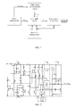
FIG. 1 is a block diagram of a driver circuit applied in a power factor corrector according to the present invention; -
FIG. 2 illustrates a specific schematic circuit diagram according to the present invention; -
FIG. 3 illustrates a specific schematic circuit diagram of alevel shift circuit 3 according to the present invention; -
FIG. 4 illustrates a specific schematic circuit diagram of a deadtime control circuit 4 according to the present invention; and -
FIG. 5 illustrates an output signal timing diagram of the deadtime control circuit 4 according to the present invention. - Reference will now be made to the drawings to describe, in detail, embodiments of the present invention. Embodiments of the invention are described more fully hereinafter with reference to the accompanying drawings. The various embodiments of the invention may, however, be embodied in many different forms and should not be construed as limited to the embodiments set forth herein.
- The terminology will be described in accordance with the definitions set out below.
- THD: Total Harmonic Distortion;
- EMI: Electromagnetic interference;
- MOS: metal oxide semiconductor;
- LDMOS: Later double-diffused metal oxide semiconductor;
- NMOS: N-channel metal oxide semiconductor FET;
- PMOS: P-channel metal oxide semiconductor FET.
- In order to make the objects, the technical solutions, and the advantages of the present invention more clearly, reference will now be made to the drawings to describe, in detail, embodiments of the present invention.
- Referring to
FIG. 1 , a high-voltage heavy-current drive circuit applied in a power factor corrector of the present invention includes: acurrent mirror circuit 1, a high-voltage pre-modulation circuit 2, alevel shift circuit 3, a deadtime control circuit 4, and a heavy-current output stage 5. - Referring to
FIG. 2 , the structure and working principle of each unit circuit of the present invention are as follows: - The current mirror circuit includes transistors Q3, Q4, Q6, Q7, Q8, Q9, Q10, Q11, Q12, Q13, and Q12 and resistors R1, R2, R3, R4, and R7. The first current mirror circuit consists of the transistor Q13 and the transistor Q14. The second current mirror circuit consists of the transistors Q3, Q4, Q6, Q7, Q8, Q9, Q10, Q11, Q12 and the resistors R1, R2, R3, R4, and R7. An input terminal of the Q14 of the first current mirror circuit is connected to an output terminal Ibias of an external reference current source. I3 is the output current of the Q13 of the first current mirror circuit, which provides a bias current for the third current mirror circuit of the high voltage pre-modulation circuit. The second current mirror circuit is the most important part of the THD optimization mechanism in the present invention. I4 is the output current of the Q7 of the second current mirror circuit, which provides a charging current for the clamp circuit. Istart is the output current of the Q8 of the first current mirror circuit, which provides mirror current for the other mirror circuit in the second current mirror circuit. In the active power factor correction controller, the required VDD voltage when the circuit is in a normal work is generally much higher, so if the transient voltage VDD reaches the desired voltage to open the circuit, an overshoot effect will occur on the output terminal, and the problems of the THD and EMI will become very serious, even the external power switch transistor will be burned. In the present invention, the THD optimization mechanism is added; when the voltage VDD lower circuit fails to work normally, the first current mirror circuit provides a start current Is:

- The current is generated at VDD> VBE_Q12; and the current is mirrored out via the mirror circuit. Firstly, the current IS is mirrored to the output current the Istart of the Q8; and the current is mirrored by the I4 to charge the clamping diodes D4 and D5, and the Q5 will be turned on. Accordingly, the output voltage VCLAMP of the high-voltage pre-modulation circuit will follow the change of the input voltage, when the instantaneous VDD reaches the desired voltage for opening the circuit, the voltage VCLAMP does not change instantaneously, the overshoot change will not occur on the output terminal. The THD is greatly optimized, and the EMI problems are reduced. Furthermore, I1 provides an output current for the Q3 of the second current mirror circuit, and I2 provides an output current for the Q4 of the second current mirror circuit, I1 and I2 provide a bias current for the level shift circuit.
- The circuit includes LDMOS transistors LDMOS1 (hereinafter referred to as high-voltage transistor LDMOS1) and LDMOS2 (hereinafter referred to as high-voltage transistor LDMOS2), zener diodes D4, D5, and D6, and a transistor Q5. The third current mirror circuit consists of the high-voltage transistor LDMOS1 and the high-voltage transistor LDMOS2. The high-voltage transistor LDMOS1 is used as the first high-voltage isolation transistor of the high-voltage pre-modulation circuit. The high-voltage transistor LDMOS2 provides a suitable bias voltage for the gate of the high-voltage transistor LDMOS1. The zener diode D6 is used as the clamping protection diode of the gate of the third current mirror circuit and is configured to ensure that the voltages of the gates of the high-voltage transistor LDMOS1 and the high-voltage transistor LDMOS2 are in the range of the breakdown voltage. The zener diodes D4 and D5 are connected in series to form the core unit of the high voltage pre-modulation circuit. When the input power supply voltage VDD is relatively high to the breakdown voltage of the zener diodes D4 and D5, while the second high voltage isolation transistor Q5 is turned on, and the output voltage VCLAMP of the high voltage pre-modulation circuit is stable at the voltage twice of the breakdown voltage of the zener diode.
- Referring to
FIG. 3 , thelevel shift circuit 3 includes high-voltage MOS transistors PMOS1, PMOS2, PMOS3, PMOS4, PMOS5, and NMOS5, high voltage NMOS transistors M3 and M4, and an inverter INV1. I1 provides an output current for the Q3 of the second current mirror circuit, and I2 provides an output current for the Q4 of the second current mirror circuit, I1 and I2 provide a current for the level shift circuit. The gates of the high-voltage MOS transistor PMOS3 and PMOS4 are connected to a collector Vb of the transistor Q9. When a pulse width modulation signal Driver is converted from a low level to a high level, a first logic switch signal S1 is converted from a high level to a low level. The NMOS transistor M3 is turned on and the NMOS transistor M4 is turned off. Under the effect of the Vb and the bias current I1, the NMOS transistor M3 is turned on, the gate voltage of the PMOS2 VA≈Vb+VGS3. The PMOS2 is also turned on, the gate voltage VB of the PMOS5 transistor approximates to the input supply voltage VCLAMP. The high voltage transistor PMOS1 and PMOS5 are turned off. After the pulse width modulation signal is delayed by the gate circuit and the capacitor, the second logic switch signal S2 is converted from a high level to a low level; and the NMOS transistor M5 is turned on, the VS outputs a low level. When the pulse width modulation signal is converted from a high level to a low level, the second logic switch signal S2 is converted from a high level to a low level, the NMOS transistor M5 is turned off. After pulse width modulation signal is delayed by the gate circuit and the capacitor, the first logic switch signal S1 is converted from a low level to a high level, the high NMOS transistor M3 is turned off, and the NMOS transistor M4 is turned on. Under the effect of the voltage Vb and input bias current I2, the high voltage transistor PMOS4 is turned on, the voltages of the gates of the PMOS1 and PMOS5 VB≈Vb+ VGS4, while the PMOS1 and PMOS5 are turned on, the voltage VA of the gate of the voltage transistor PMOS2 approximates to the input supply voltage VCLAMP. The high voltage transistor PMOS2 is turned off, the VS outputs a high level. After the dead time control circuit is added, the phenomenon of the transient heavy-current from the power supply to the ground during the level conversion is prevented. - Referring to
FIG. 4 and FIG. 5 , the deadtime control circuit 4 is configured to generate an inverse non-overlapping first logic switch signal S1 and second logic switch signal S2 using a pulse width modulation signal Driver in the switching power supply. when the pulse width modulation signal is converted from the low level to the high level, the first logic switch signal S1 is converted from a high level to a low level, after the pulse width modulation signal is delayed by the gate circuit and the capacitor, the second logic switch signal S2 is converted from a high level to a low level. When the pulse width modulation signal is converted from a high level to a low level, the second logic switch signal S2 is converted from a high level to a low level, after the pulse width modulation signal is delayed by the gate circuit and the capacitor, the first logicswitch signal S 1 is converted from a low level to a high level. - Referring to
FIG. 2 ,FIG. 4, and FIG. 5 , the heavy-current output stage 5 includes a Darlington configuration with a great sink current capability and a combined high voltage NMOS pull-down transistor with a great source current capability. The Darlington configuration consists of transistors Q1 and Q2, diodes D1 and D2. The combined high voltage NMOS pull-down transistor consists of high voltage NMOS transistors M1, M2, and M5, resistors R5 and R6. When the pulse width modulation signal Driver is at high level, the first logic switch signal S1 of the dead time control circuit is at low level, the second logic switch signal S2 is at high level, the output signal VS of the level shift circuit is at low level. Under the effect of the high voltage NMOS transistors M1, M2, and M5, the output GATE_DRIVER of the heavy-current output stage is pulled down. When the pulse width modulation signal Driver is at low level, the first logic switch signal S1 of the dead time control circuit is at high level, the second logic switch signal S2 is at low level, the high voltage NMOS pull-down transistors M1, M2 and M5 are in the off state, the output signal VS of the level shift circuit is at high level. Under the effect of the Darlington transistors Q1 and Q2, the output GATE_DRIVER of the heavy-current output stage is quickly charged to the high level. The resistors R5 and R6 of the heavy-current output stage are also the important parts of the THD optimization mechanism in the present invention. The main role of the resistors R5 and R6 is to limit the current of the output stage, and to prevent the output stage from generating transient overshoot, thus the THD is optimized. Furthermore, since the output drive signal GATE_DRIVER is connected to the peripheral power devices via a pin of a chip, a parasitic inductance is generated. An LC resonance circuit consists of the parasitic inductance and a gate parasitic capacitance of the power devices. After suitable resistors are added to the output stage circuit, during the level conversion of the output drive signal, the oscillation of the output drive signal is effectively inhibited to reduce the EMI problems. When the output drive signal GATE_DRIVER is converted from a high level to a low level, the diodes D1 and D2 provide a fast discharge path to the base of the Q1 and Q2 of the Darlington transistors to accelerate the shutdown of the Darlington combined transistors Q1 and Q2. - The present invention utilizes the isolation of the high-voltage LDMOS transistor and breakdown voltage characteristics of the zener diode, the higher input supply voltage is converted to the fixed level desired for the output driver switch signal, not only the reliability of the drive circuit is improved, but also the peripheral power devices are effectively protected. The present invention utilizes the level shift circuit; the pulse width modulation signal generated from the digital logic drive circuit is converted to a fixed level of the output drive switching signal, while the dead time control circuit is added to prevent the phenomenon of the transient heavy-current from the power supply to the ground during the level conversion. The present invention uses the classic Darlington output stage structure to improve the capability of the source current and sink current of the output driver circuit. For the requirements of the active power factor correction circuit for the total harmonic distortion (THD), a THD optimization mechanism is added in the sub-module circuit to reduce the THD.
- Although the present invention has been described with reference to the embodiments thereof and the best modes for carrying out the present invention, it is apparent to those skilled in the art that a variety of modifications and changes may be made without departing from the scope of the present invention, which is intended to be defined by the appended claims..
Claims (7)
- A high-voltage heavy-current drive circuit applied in a power factor corrector, comprising a current mirror circuit (1), a high-voltage pre-modulation circuit (2), a level shift circuit (3), a dead time control circuit (4), and a heavy-current output stage (5);
wherein the current mirror circuit (1) is configured to convert an input signal Ibias to an input signal of the high voltage pre-modulation circuit using a current source circuit and a current sink circuit composed of a plurality of resistors and transistors, the input signal Ibias is generated by a starting current Istart and a reference current source, and the starting current Istart is converted to an input signal of the level shift circuit;
under an effect of a bias of the current mirror circuit (1), the high voltage pre-modulation circuit (2) is configured to convert a high input supply voltage VDD to a relative low voltage using an isolation of a high-voltage LDMOS transistor and stabilized breakdown voltage characteristics of a zener diode to ensure the drive circuit operating within a safe voltage range, and to generate an input voltage VCLAMP of the level shift circuit;
under effects of an output of the high-voltage pre-modulation circuit (2) and the bias of the current mirror circuit (1), the level shift circuit (3) is configured to control on and off states of a high-voltage transistor PMOS and a high-voltage transistor NOMS using a first logic switch signal S1 and a second switch logic signal S2 generated by the dead time control circuit; thereby generating an output signal Vs of the level shift circuit to provide a logic switch signal for the heavy-current output stage;
under an effect of an digital logic drive signal, using delays of a logic gate circuit and capacitors, the dead time control circuit (4) is configured to generate inverse non-overlapping first logic switch signal S1 and second logic switch signal S2, and to control operating states of the level shift circuit and the heavy-current output stage;
under an effect of a Darlington composed of high voltage transistors, using the logic switch signal VS generated by the high-voltage transistor NOMS and the level shift circuit and a second logic switch signal S2 generated by the dead time control circuit, the high current output stage (3) is configured to generate an output drive signal GATE_DRIVER with great source current capability and sink current capability and to drive on and off states of an external power device. - The high-voltage heavy-current drive circuit according to claim 1, wherein the current mirror circuit (1) comprises transistors Q3, Q4, Q6, Q7, Q8, Q9, Q10, Q11, Q12, Q13, and Q14, and resistors R1, R2, R3, R4, and R7; a first current mirror circuit consists of the transistor Q13 and the transistor Q14; a second current mirror circuit consists of the transistors Q3, Q4, Q6, Q7, Q8, Q9, Q10, Q11, and Q12 and the resistors R1, R2, R3, R4, and R7; an input terminal of the first current mirror circuit is connected to an output terminal Ibias of an external reference current source; the first current mirror circuit is configured to provide a bias current for the high-voltage pre-modulation circuit when the circuit is operating normally; the second current mirror circuit is configured to provide a bias current for the high-voltage pre-modulation circuit and the level shift circuit.
- The high-voltage heavy-current drive circuit according to claim 1, wherein the high-voltage pre-modulation circuit comprises an LDMOS transistor LDMOS1, an LDMOS transistor LDMOS2, zener diodes D4, D5, and D6, and a transistor Q5; a third current mirror circuit consists of the LDMOS transistor LDMOS1 and the LDMOS transistors LDMOS2; the LDMOS transistor LDMOS1 is used as a first high-voltage insulating transistor of the high pre-modulation circuit; the LDMOS transistor LDMOS2 is used as a gate bias transistor of the LDMOS transistor LDMOS1; the zener diode D6 is used as a gate clamping protection of the third current mirror circuit; the zener diodes D4 and D5 are connected in series to form a first high-voltage pre-modulation circuit; the transistor Q5 is used as a second high-voltage insulating transistor of the high pre-modulation circuit.
- The high-voltage heavy-current drive circuit according to claim 3, wherein in the high-voltage pre-modulation circuit (2), a gate and a drain of the LDMOS transistor LDMOS2 in the third current mirror circuit are connected together and connected to an output terminal of a collector of the transistor Q13 in the first current mirror circuit; a source of the LDMOS transistor LDMOS1 and the LDMOS transistors LDMOS2 is connected to the input power supply VDD; a clamping diode D6 is coupled between the gate and the source of the LDMOS transistor LDMOS1 and the LDMOS transistors LDMOS2 in the third current mirror circuit; a drain terminal of the LDMOS transistor LDMOS1 is connected to an N terminal of clamping diodes D4 and D5 connected in series, and also connected to a base of the transistor Q5, and an output terminal of a collector of the transistor Q7 in the second current mirror circuit; a high voltage pre-modulation signal VCLAMP is generated on an emitter of the transistor Q5.
- The high-voltage heavy-current drive circuit according to claim 1, wherein the level shift circuit (3) comprises high-voltage PMOS transistors, PMOS1, PMOS2, PMOS3, PMOS4, and PMOS5, high-voltage NMOS transistors M3, M4, and M5, and an inverter INV1;
a source of the high-voltage PMOS transistors, PMOS1, PMOS2, and PMOS5 is connected to a common power supply VCLAMP, namely, is connected to an output terminal of the high-voltage pre-modulation circuit (2);
a gate of the high-voltage PMOS transistor PMOS1 is connected to a drain of the high-voltage PMOS transistor PMOS2, a drain of the high-voltage PMOS transistor PMOS1 is connected to a gate of the high-voltage PMOS transistor PMOS2 and a source of the high-voltage PMOS transistor PMOS3;
under an effect of a bias of a second current mirror circuit in the current mirror circuit, a collector of an output terminal of a transistor Q3 of the second current mirror circuit is connected to the drain of the high-voltage PMOS transistor PMOS1, the gate of the high-voltage PMOS transistor PMOS2, and the source of the high-voltage PMOS transistor PMOS3 to be a bias current of the level shift circuit;
the gate of the high-voltage PMOS transistor PMOS2 is connected to the drain of the high-voltage PMOS transistor PMOS1; the drain of the high-voltage PMOS transistor PMOS2 is connected to the gate of the high-voltage PMOS transistor PMOS1, a source of the high-voltage PMOS transistor PMOS4, and a gate of the high-voltage PMOS transistor PMOS5;
under an effect of the bias of the second current mirror circuit in the current mirror circuit (1), an output terminal of a collector of a transistor Q4 of the second current mirror circuit is connected to the gate of the high-voltage PMOS transistor PMOS1, the source of the high-voltage PMOS transistor PMOS4, and the gate of the high-voltage PMOS transistor PMOS5 to provide a bias current for the level shift circuit (3);
the gates of the high-voltage PMOS transistors PMOS3 and PMOS4 are connected to a common terminal Vb; the drain of the high-voltage PMOS transistors PMOS3 is connected to a drain of the high-voltage NMOS transistor M3; the drain of the high-voltage PMOS transistors PMOS4 is connected to a drain of the high-voltage NMOS transistor M4; a gate of the high-voltage NMOS transistor M3 is connected to an output terminal of the inverter INV1; a source of the high-voltage NMOS transistor M3 is connected to a common terminal GND;
an input terminal of the inverter INV1 is connected to the first logic switch signal S1 generated by the dead time control circuit; a gate of the high-voltage NMOS transistor M4 is connected to the input terminal of inverter INV1, namely, is connected to the first logic switch signal S1; a source of the high-voltage NMOS transistor M4 is connected to the common GND; the gate of the high-voltage NMOS transistor PMOS5 is connected to the drain of the high-voltage NMOS transistor M2, the gate of the PMOS1, and the source of the PMOS4; the source of the high-voltage NMOS transistor PMOS5 is connected to the output VCLAMP of the high voltage pre-modulation circuit (2);
the drain of the high-voltage PMOS transistor PMOS5 is connected to the drain of high-voltage NMOS transistor M5; the gate of the high-voltage NMOS transistor M5 is connected to the second switch logic signal S2 generated by the dead time control circuit; the drain of the high-voltage NMOS transistor M5 is connected to the common ground terminal GND; the drain of the high-voltage PMOS transistors PMOS5 and the drain of the high-voltage NMOS transistors PMOS5 are connected together to generate the output signal Vs of the level shift circuit, and to control the turn-on state and the turn-off state of the heavy-current output stage (5). - The high-voltage heavy-current drive circuit according to claim 1, wherein the dead time control circuit (4) is configured to generate inverse non-overlapping first logic switch signal S1 and second logic switch signal S2 using a pulse width modulation signal in the switching power supply;
when the pulse width modulation signal is converted from a low level to a high level, the first logic switch signal S1 is converted from a high level to a low level, then the pulse width modulation signal is delayed by the gate circuit and the capacitor, and the second logic switch signal S2 is converted from a high level to a low level;
when the pulse width modulation signal is converted from a high level to a low level, the second logic switch signal S2 is converted from a high level to a low level, then the pulse width modulation signal is delayed by the gate circuit and the capacitor, and the first logic switch signal S1 is converted from a low level to a high level. - The high-voltage heavy-current drive circuit according to claim 1, wherein the heavy-current output stage (5) comprises a Darlington configuration with a great sink current capability and a combined high voltage NMOS pull-down transistor with a great source current capability;
the Darlington configuration consists of transistors Q1 and Q2, diodes D1 and D2;
a collector of the Q1 and Q2 is connected to a common power supply VDD; a base of the transistor Q2 is connected to an N-terminal of the diode D2 and an end of the resistor R5; the N-terminal of the diode D2 and the end of the resistor R5 are connected to an output terminal VS of the level shift circuit; an emitter of transistor Q2 is connected to a P-terminal of the diode D2, an N-terminal of the diode D1, the other end of the resistor R5, an end of the resistor R6, and a base of the transistor Q1;
an emitter of the transistor Q1 is connected to the other end of the resistor R6, and a P-terminal of the diode D1; the other end of the resistor R6 and the P- terminal of the diode D1 are connected to an output terminal GATE_DRIVER of the high current output stage; the combined high voltage NMOS pull-down transistor consists of high-voltage NMOS transistors M1, M2 and M5 and resistors R5 and R6;
a drain of the high-voltage NMOS transistor M1 is connected to an emitter of transistor Q1 and an end of the resistor R6; the emitter of transistor Q1 and the end of the resistor R6 are connected to the output stage GATE_DRIVER of the high current output stage; a drain of the high-voltage NMOS transistor M2 is connected to a base of transistor Q1, an emitter of transistor Q2, the N-terminal of the diode D1, and the P- terminal of the diode D2; a drain of the high-voltage NMOS transistors M5 is connected to a base of transistor Q2 and an end of the resistor R5; the base of transistor Q2 and the end of the resistor R5 are connected to the output VS of the level shifter circuit; the gates of the high-voltage NMOS transistors M1, M2 and M5 are connected together and connected to the second switch logic signal S2 generated by the dead time control circuit; the sources of the high-voltage NMOS transistors M1, M2 and M5 are connected to the common ground GND.
Applications Claiming Priority (2)
| Application Number | Priority Date | Filing Date | Title |
|---|---|---|---|
| CN201110363627.XA CN102403902B (en) | 2011-11-16 | 2011-11-16 | High-voltage and large-current driving circuit applied to power factor corrector |
| PCT/CN2012/084379 WO2013071842A1 (en) | 2011-11-16 | 2012-11-09 | High-voltage heavy-current drive circuit applied in power factor corrector |
Publications (3)
| Publication Number | Publication Date |
|---|---|
| EP2782233A1 true EP2782233A1 (en) | 2014-09-24 |
| EP2782233A4 EP2782233A4 (en) | 2015-06-24 |
| EP2782233B1 EP2782233B1 (en) | 2019-01-02 |
Family
ID=45885787
Family Applications (1)
| Application Number | Title | Priority Date | Filing Date |
|---|---|---|---|
| EP12850584.9A Active EP2782233B1 (en) | 2011-11-16 | 2012-11-09 | High-voltage heavy-current drive circuit applied in power factor corrector |
Country Status (4)
| Country | Link |
|---|---|
| US (1) | US9190897B2 (en) |
| EP (1) | EP2782233B1 (en) |
| CN (1) | CN102403902B (en) |
| WO (1) | WO2013071842A1 (en) |
Cited By (1)
| Publication number | Priority date | Publication date | Assignee | Title |
|---|---|---|---|---|
| US11444337B2 (en) | 2019-03-12 | 2022-09-13 | Samsung Sdi Co., Ltd | Solid state switch driver circuit for a battery system |
Families Citing this family (28)
| Publication number | Priority date | Publication date | Assignee | Title |
|---|---|---|---|---|
| CN102403902B (en) * | 2011-11-16 | 2014-02-05 | 无锡华润上华科技有限公司 | High-voltage and large-current driving circuit applied to power factor corrector |
| CN102843123B (en) * | 2012-08-31 | 2015-09-09 | 电子科技大学 | A kind of high-voltage driving circuit |
| US9438240B1 (en) * | 2015-08-31 | 2016-09-06 | Cypress Semiconductor Corporation | Biasing circuit for level shifter with isolation |
| CN105634461B (en) * | 2015-12-28 | 2018-11-20 | 上海数明半导体有限公司 | A kind of level shift circuit |
| JP6747371B2 (en) * | 2017-04-26 | 2020-08-26 | 三菱電機株式会社 | High voltage level shift circuit and driving device |
| JP6917793B2 (en) * | 2017-06-13 | 2021-08-11 | ローム株式会社 | Current adjustment circuit, power supply management circuit using it |
| US10608625B1 (en) | 2018-09-18 | 2020-03-31 | Infineon Technologies Austria Ag | Gate driver with continuously-variable current |
| CN109459622B (en) * | 2018-10-24 | 2021-02-05 | 江南大学 | Low-power-consumption CMOS squelch detector |
| CN109474246B (en) * | 2018-10-31 | 2022-06-28 | 西安微电子技术研究所 | Voltage clamping protection structure and operational amplifier input stage structure |
| CN109547009B (en) * | 2018-11-19 | 2022-08-12 | 中国电子科技集团公司第五十八研究所 | High reliability level shift circuit |
| CN109245535A (en) * | 2018-11-20 | 2019-01-18 | 广州市力驰微电子科技有限公司 | Level switch module suitable for power management |
| WO2021109145A1 (en) * | 2019-12-06 | 2021-06-10 | 辉芒微电子(深圳)有限公司 | Darlington transistor driving circuit, method, and constant current switch power supply |
| CN111313883B (en) * | 2020-02-26 | 2022-01-25 | 中国电子科技集团公司第五十八研究所 | Power driving circuit based on bipolar device |
| CN112583368A (en) * | 2020-12-10 | 2021-03-30 | 中国电子科技集团公司第十四研究所 | High-power GaN power amplifier modulation circuit |
| CN113949260B (en) * | 2021-09-08 | 2023-06-06 | 中国电子科技集团公司第五十五研究所 | A high-speed high-voltage high-current modulation circuit |
| CN114077232A (en) * | 2021-11-03 | 2022-02-22 | 西安热工研究院有限公司 | High-current driving system and method for steam turbine servo valve |
| CN114442715B (en) * | 2021-12-29 | 2023-08-18 | 中国航空工业集团公司西安航空计算技术研究所 | 28V or open circuit discrete quantity output circuit |
| CN114598138A (en) * | 2022-03-11 | 2022-06-07 | 苏州锴威特半导体股份有限公司 | A power tube gate terminal drive circuit |
| CN115001247B (en) * | 2022-06-02 | 2024-06-04 | 上海安路信息科技股份有限公司 | High-voltage-resistant high-speed driving circuit |
| CN115425963B (en) * | 2022-08-05 | 2025-10-24 | 西安电子科技大学芜湖研究院 | An isolated transmission circuit |
| CN115469242B (en) * | 2022-09-13 | 2024-01-12 | 江苏万邦微电子有限公司 | Negative power supply monitoring system and method |
| CN116232021A (en) * | 2023-03-27 | 2023-06-06 | 屹晶微电子(台州)有限公司 | A high-voltage half-bridge drive circuit and integrated chip |
| CN117155079B (en) * | 2023-10-30 | 2024-01-16 | 晶艺半导体有限公司 | Driving circuit applied to power switch and power management chip |
| CN118367904B (en) * | 2024-06-14 | 2024-08-27 | 深圳市晶扬电子有限公司 | Switch enabling circuit with low static power consumption and suitable for high and low voltage |
| CN119652310B (en) * | 2024-11-29 | 2025-12-05 | 湖南大学 | A high-voltage level displacement circuit with adaptive dead time |
| CN121049565B (en) * | 2025-11-05 | 2026-01-20 | 浙江大学 | Current detection circuit and current detection method for high voltage power supply |
| CN121395888B (en) * | 2025-12-24 | 2026-05-05 | 成都信息工程大学 | BUCK upper tube driving circuit |
| CN121680557B (en) * | 2026-02-06 | 2026-05-05 | 英彼森半导体(珠海)有限公司 | A driving voltage generation circuit |
Family Cites Families (18)
| Publication number | Priority date | Publication date | Assignee | Title |
|---|---|---|---|---|
| US4278929A (en) * | 1979-11-21 | 1981-07-14 | Motorola, Inc. | Regulated negative voltage supply |
| US4725741A (en) * | 1985-11-13 | 1988-02-16 | Sundstrand Corporation | Drive circuit for fast switching of Darlington-connected transistors |
| US5896043A (en) * | 1989-02-10 | 1999-04-20 | Fuji Electric Co., Ltd. | Level shift circuit |
| US5045721A (en) * | 1989-03-16 | 1991-09-03 | Teledyne Industries | Zero static current high speed TTL compatible buffer |
| US5087841A (en) * | 1990-04-09 | 1992-02-11 | National Semiconductor Corporation | TTL to CMOS translating circuits without static current |
| US5502370A (en) * | 1994-09-06 | 1996-03-26 | Motorola, Inc. | Power factor control circuit having a boost current for increasing a speed of a voltage control loop and method therefor |
| US5861736A (en) * | 1994-12-01 | 1999-01-19 | Texas Instruments Incorporated | Circuit and method for regulating a voltage |
| IT1318794B1 (en) * | 2000-08-29 | 2003-09-10 | St Microelectronics Srl | CIRCUIT FOR PILOTING A POWER SWITCH. |
| DE10157292A1 (en) * | 2001-11-22 | 2003-06-05 | Infineon Technologies Ag | Temperature stabilized oscillator circuit |
| US7113017B2 (en) * | 2004-07-01 | 2006-09-26 | Intersil Americas Inc. | Floating gate analog voltage level shift circuit and method for producing a voltage reference that operates on a low supply voltage |
| CN101506753B (en) * | 2006-08-07 | 2012-07-18 | 意法半导体股份有限公司 | Control device for devices for power factor correction in forced switching power supplies |
| CN100530919C (en) * | 2007-02-06 | 2009-08-19 | 西安交通大学 | Single chip high frequency DC-DC converter |
| US7808304B1 (en) * | 2007-04-09 | 2010-10-05 | Marvell International Ltd. | Current switch for high voltage process |
| JP2008289319A (en) * | 2007-05-21 | 2008-11-27 | Sanken Electric Co Ltd | Discharge tube power supply system and semiconductor integrated circuit |
| CN101697454B (en) * | 2009-10-30 | 2011-09-14 | 北京航星力源科技有限公司 | Grid drive circuit of insulated grid device |
| US8476836B2 (en) * | 2010-05-07 | 2013-07-02 | Cree, Inc. | AC driven solid state lighting apparatus with LED string including switched segments |
| US8866412B2 (en) * | 2011-01-11 | 2014-10-21 | Braxton Engineering, Inc. | Source and multiple loads regulator |
| CN102403902B (en) | 2011-11-16 | 2014-02-05 | 无锡华润上华科技有限公司 | High-voltage and large-current driving circuit applied to power factor corrector |
-
2011
- 2011-11-16 CN CN201110363627.XA patent/CN102403902B/en active Active
-
2012
- 2012-11-09 EP EP12850584.9A patent/EP2782233B1/en active Active
- 2012-11-09 WO PCT/CN2012/084379 patent/WO2013071842A1/en not_active Ceased
- 2012-11-09 US US14/358,566 patent/US9190897B2/en active Active
Cited By (1)
| Publication number | Priority date | Publication date | Assignee | Title |
|---|---|---|---|---|
| US11444337B2 (en) | 2019-03-12 | 2022-09-13 | Samsung Sdi Co., Ltd | Solid state switch driver circuit for a battery system |
Also Published As
| Publication number | Publication date |
|---|---|
| CN102403902A (en) | 2012-04-04 |
| CN102403902B (en) | 2014-02-05 |
| WO2013071842A1 (en) | 2013-05-23 |
| US9190897B2 (en) | 2015-11-17 |
| EP2782233B1 (en) | 2019-01-02 |
| EP2782233A4 (en) | 2015-06-24 |
| US20140293664A1 (en) | 2014-10-02 |
Similar Documents
| Publication | Publication Date | Title |
|---|---|---|
| EP2782233B1 (en) | High-voltage heavy-current drive circuit applied in power factor corrector | |
| US10355593B1 (en) | Circuits for three-level buck regulators | |
| US8638134B2 (en) | Gate drive circuit and power semiconductor module | |
| CN113162373B (en) | An all-GaN integrated gate driver circuit with dead-time control | |
| CN107086863B (en) | Driving circuit for power switch | |
| CN104410300A (en) | Synchronous rectification drive circuit and television set | |
| JPH02214219A (en) | Bipolar mos tri-state output buffer | |
| CN115389893B (en) | Negative pressure detection circuit | |
| CN114696573A (en) | The structure of gate drive circuit for improving gate voltage of power MOS transistor in bootstrap circuit | |
| JP2012004786A (en) | Level shift circuit and switching power supply device | |
| Ming et al. | A GaN HEMT gate driver IC with programmable turn-on dV/dt control | |
| CN115776297A (en) | Grid driving integrated circuit with low power consumption and wide power supply voltage range | |
| CN115411922A (en) | Buffer for absorbing current | |
| JP5352708B2 (en) | Gate drive device | |
| CN107579728B (en) | Driving circuit of power field effect transistor adopting charge pump | |
| CN112886798B (en) | MOS field effect transistor driving circuit and control method | |
| US11979144B2 (en) | Driving circuit for driving chip | |
| Mandelli et al. | Active dual level gate driver for dead time and switching losses reduction in drive systems | |
| CN214480548U (en) | High-voltage driving circuit | |
| TW202425513A (en) | Control device for power conversion apparatus | |
| CN111953216B (en) | Driving circuit of synchronous rectification circuit and driving method thereof | |
| CN110113035B (en) | High-frequency power MOSFET drive circuit | |
| CN110380599B (en) | A hybrid gate drive circuit | |
| TWI465020B (en) | Can produce three times the input voltage of the gate driver and drive method | |
| CN114362729A (en) | Gate drive circuit adaptive to high junction temperature environment and switching-on method and switching-off method thereof |
Legal Events
| Date | Code | Title | Description |
|---|---|---|---|
| PUAI | Public reference made under article 153(3) epc to a published international application that has entered the european phase |
Free format text: ORIGINAL CODE: 0009012 |
|
| 17P | Request for examination filed |
Effective date: 20140521 |
|
| AK | Designated contracting states |
Kind code of ref document: A1 Designated state(s): AL AT BE BG CH CY CZ DE DK EE ES FI FR GB GR HR HU IE IS IT LI LT LU LV MC MK MT NL NO PL PT RO RS SE SI SK SM TR |
|
| DAX | Request for extension of the european patent (deleted) | ||
| RA4 | Supplementary search report drawn up and despatched (corrected) |
Effective date: 20150528 |
|
| RIC1 | Information provided on ipc code assigned before grant |
Ipc: H03K 17/0412 20060101ALI20150521BHEP Ipc: H03K 17/687 20060101ALI20150521BHEP Ipc: H02M 1/42 20070101ALI20150521BHEP Ipc: H02M 1/08 20060101AFI20150521BHEP Ipc: H03K 17/16 20060101ALI20150521BHEP Ipc: H03K 17/615 20060101ALI20150521BHEP |
|
| GRAP | Despatch of communication of intention to grant a patent |
Free format text: ORIGINAL CODE: EPIDOSNIGR1 |
|
| STAA | Information on the status of an ep patent application or granted ep patent |
Free format text: STATUS: GRANT OF PATENT IS INTENDED |
|
| INTG | Intention to grant announced |
Effective date: 20180420 |
|
| GRAJ | Information related to disapproval of communication of intention to grant by the applicant or resumption of examination proceedings by the epo deleted |
Free format text: ORIGINAL CODE: EPIDOSDIGR1 |
|
| STAA | Information on the status of an ep patent application or granted ep patent |
Free format text: STATUS: REQUEST FOR EXAMINATION WAS MADE |
|
| GRAP | Despatch of communication of intention to grant a patent |
Free format text: ORIGINAL CODE: EPIDOSNIGR1 |
|
| STAA | Information on the status of an ep patent application or granted ep patent |
Free format text: STATUS: GRANT OF PATENT IS INTENDED |
|
| INTC | Intention to grant announced (deleted) | ||
| INTG | Intention to grant announced |
Effective date: 20180606 |
|
| GRAS | Grant fee paid |
Free format text: ORIGINAL CODE: EPIDOSNIGR3 |
|
| GRAA | (expected) grant |
Free format text: ORIGINAL CODE: 0009210 |
|
| STAA | Information on the status of an ep patent application or granted ep patent |
Free format text: STATUS: THE PATENT HAS BEEN GRANTED |
|
| AK | Designated contracting states |
Kind code of ref document: B1 Designated state(s): AL AT BE BG CH CY CZ DE DK EE ES FI FR GB GR HR HU IE IS IT LI LT LU LV MC MK MT NL NO PL PT RO RS SE SI SK SM TR |
|
| REG | Reference to a national code |
Ref country code: GB Ref legal event code: FG4D |
|
| REG | Reference to a national code |
Ref country code: CH Ref legal event code: EP Ref country code: AT Ref legal event code: REF Ref document number: 1085669 Country of ref document: AT Kind code of ref document: T Effective date: 20190115 |
|
| REG | Reference to a national code |
Ref country code: IE Ref legal event code: FG4D |
|
| REG | Reference to a national code |
Ref country code: DE Ref legal event code: R096 Ref document number: 602012055539 Country of ref document: DE |
|
| REG | Reference to a national code |
Ref country code: NL Ref legal event code: FP |
|
| REG | Reference to a national code |
Ref country code: LT Ref legal event code: MG4D |
|
| REG | Reference to a national code |
Ref country code: AT Ref legal event code: MK05 Ref document number: 1085669 Country of ref document: AT Kind code of ref document: T Effective date: 20190102 |
|
| PG25 | Lapsed in a contracting state [announced via postgrant information from national office to epo] |
Ref country code: NO Free format text: LAPSE BECAUSE OF FAILURE TO SUBMIT A TRANSLATION OF THE DESCRIPTION OR TO PAY THE FEE WITHIN THE PRESCRIBED TIME-LIMIT Effective date: 20190402 Ref country code: FI Free format text: LAPSE BECAUSE OF FAILURE TO SUBMIT A TRANSLATION OF THE DESCRIPTION OR TO PAY THE FEE WITHIN THE PRESCRIBED TIME-LIMIT Effective date: 20190102 Ref country code: LT Free format text: LAPSE BECAUSE OF FAILURE TO SUBMIT A TRANSLATION OF THE DESCRIPTION OR TO PAY THE FEE WITHIN THE PRESCRIBED TIME-LIMIT Effective date: 20190102 Ref country code: SE Free format text: LAPSE BECAUSE OF FAILURE TO SUBMIT A TRANSLATION OF THE DESCRIPTION OR TO PAY THE FEE WITHIN THE PRESCRIBED TIME-LIMIT Effective date: 20190102 Ref country code: PL Free format text: LAPSE BECAUSE OF FAILURE TO SUBMIT A TRANSLATION OF THE DESCRIPTION OR TO PAY THE FEE WITHIN THE PRESCRIBED TIME-LIMIT Effective date: 20190102 Ref country code: ES Free format text: LAPSE BECAUSE OF FAILURE TO SUBMIT A TRANSLATION OF THE DESCRIPTION OR TO PAY THE FEE WITHIN THE PRESCRIBED TIME-LIMIT Effective date: 20190102 Ref country code: PT Free format text: LAPSE BECAUSE OF FAILURE TO SUBMIT A TRANSLATION OF THE DESCRIPTION OR TO PAY THE FEE WITHIN THE PRESCRIBED TIME-LIMIT Effective date: 20190502 |
|
| PG25 | Lapsed in a contracting state [announced via postgrant information from national office to epo] |
Ref country code: RS Free format text: LAPSE BECAUSE OF FAILURE TO SUBMIT A TRANSLATION OF THE DESCRIPTION OR TO PAY THE FEE WITHIN THE PRESCRIBED TIME-LIMIT Effective date: 20190102 Ref country code: GR Free format text: LAPSE BECAUSE OF FAILURE TO SUBMIT A TRANSLATION OF THE DESCRIPTION OR TO PAY THE FEE WITHIN THE PRESCRIBED TIME-LIMIT Effective date: 20190403 Ref country code: BG Free format text: LAPSE BECAUSE OF FAILURE TO SUBMIT A TRANSLATION OF THE DESCRIPTION OR TO PAY THE FEE WITHIN THE PRESCRIBED TIME-LIMIT Effective date: 20190402 Ref country code: LV Free format text: LAPSE BECAUSE OF FAILURE TO SUBMIT A TRANSLATION OF THE DESCRIPTION OR TO PAY THE FEE WITHIN THE PRESCRIBED TIME-LIMIT Effective date: 20190102 Ref country code: IS Free format text: LAPSE BECAUSE OF FAILURE TO SUBMIT A TRANSLATION OF THE DESCRIPTION OR TO PAY THE FEE WITHIN THE PRESCRIBED TIME-LIMIT Effective date: 20190502 Ref country code: HR Free format text: LAPSE BECAUSE OF FAILURE TO SUBMIT A TRANSLATION OF THE DESCRIPTION OR TO PAY THE FEE WITHIN THE PRESCRIBED TIME-LIMIT Effective date: 20190102 |
|
| REG | Reference to a national code |
Ref country code: DE Ref legal event code: R097 Ref document number: 602012055539 Country of ref document: DE |
|
| PG25 | Lapsed in a contracting state [announced via postgrant information from national office to epo] |
Ref country code: AT Free format text: LAPSE BECAUSE OF FAILURE TO SUBMIT A TRANSLATION OF THE DESCRIPTION OR TO PAY THE FEE WITHIN THE PRESCRIBED TIME-LIMIT Effective date: 20190102 Ref country code: DK Free format text: LAPSE BECAUSE OF FAILURE TO SUBMIT A TRANSLATION OF THE DESCRIPTION OR TO PAY THE FEE WITHIN THE PRESCRIBED TIME-LIMIT Effective date: 20190102 Ref country code: AL Free format text: LAPSE BECAUSE OF FAILURE TO SUBMIT A TRANSLATION OF THE DESCRIPTION OR TO PAY THE FEE WITHIN THE PRESCRIBED TIME-LIMIT Effective date: 20190102 Ref country code: SK Free format text: LAPSE BECAUSE OF FAILURE TO SUBMIT A TRANSLATION OF THE DESCRIPTION OR TO PAY THE FEE WITHIN THE PRESCRIBED TIME-LIMIT Effective date: 20190102 Ref country code: IT Free format text: LAPSE BECAUSE OF FAILURE TO SUBMIT A TRANSLATION OF THE DESCRIPTION OR TO PAY THE FEE WITHIN THE PRESCRIBED TIME-LIMIT Effective date: 20190102 Ref country code: EE Free format text: LAPSE BECAUSE OF FAILURE TO SUBMIT A TRANSLATION OF THE DESCRIPTION OR TO PAY THE FEE WITHIN THE PRESCRIBED TIME-LIMIT Effective date: 20190102 Ref country code: RO Free format text: LAPSE BECAUSE OF FAILURE TO SUBMIT A TRANSLATION OF THE DESCRIPTION OR TO PAY THE FEE WITHIN THE PRESCRIBED TIME-LIMIT Effective date: 20190102 Ref country code: CZ Free format text: LAPSE BECAUSE OF FAILURE TO SUBMIT A TRANSLATION OF THE DESCRIPTION OR TO PAY THE FEE WITHIN THE PRESCRIBED TIME-LIMIT Effective date: 20190102 |
|
| PLBE | No opposition filed within time limit |
Free format text: ORIGINAL CODE: 0009261 |
|
| STAA | Information on the status of an ep patent application or granted ep patent |
Free format text: STATUS: NO OPPOSITION FILED WITHIN TIME LIMIT |
|
| PG25 | Lapsed in a contracting state [announced via postgrant information from national office to epo] |
Ref country code: SM Free format text: LAPSE BECAUSE OF FAILURE TO SUBMIT A TRANSLATION OF THE DESCRIPTION OR TO PAY THE FEE WITHIN THE PRESCRIBED TIME-LIMIT Effective date: 20190102 |
|
| 26N | No opposition filed |
Effective date: 20191003 |
|
| PG25 | Lapsed in a contracting state [announced via postgrant information from national office to epo] |
Ref country code: SI Free format text: LAPSE BECAUSE OF FAILURE TO SUBMIT A TRANSLATION OF THE DESCRIPTION OR TO PAY THE FEE WITHIN THE PRESCRIBED TIME-LIMIT Effective date: 20190102 |
|
| PG25 | Lapsed in a contracting state [announced via postgrant information from national office to epo] |
Ref country code: TR Free format text: LAPSE BECAUSE OF FAILURE TO SUBMIT A TRANSLATION OF THE DESCRIPTION OR TO PAY THE FEE WITHIN THE PRESCRIBED TIME-LIMIT Effective date: 20190102 |
|
| REG | Reference to a national code |
Ref country code: CH Ref legal event code: PL |
|
| PG25 | Lapsed in a contracting state [announced via postgrant information from national office to epo] |
Ref country code: LU Free format text: LAPSE BECAUSE OF NON-PAYMENT OF DUE FEES Effective date: 20191109 Ref country code: MC Free format text: LAPSE BECAUSE OF FAILURE TO SUBMIT A TRANSLATION OF THE DESCRIPTION OR TO PAY THE FEE WITHIN THE PRESCRIBED TIME-LIMIT Effective date: 20190102 Ref country code: LI Free format text: LAPSE BECAUSE OF NON-PAYMENT OF DUE FEES Effective date: 20191130 Ref country code: CH Free format text: LAPSE BECAUSE OF NON-PAYMENT OF DUE FEES Effective date: 20191130 |
|
| REG | Reference to a national code |
Ref country code: BE Ref legal event code: MM Effective date: 20191130 |
|
| PG25 | Lapsed in a contracting state [announced via postgrant information from national office to epo] |
Ref country code: IE Free format text: LAPSE BECAUSE OF NON-PAYMENT OF DUE FEES Effective date: 20191109 |
|
| PG25 | Lapsed in a contracting state [announced via postgrant information from national office to epo] |
Ref country code: BE Free format text: LAPSE BECAUSE OF NON-PAYMENT OF DUE FEES Effective date: 20191130 |
|
| PG25 | Lapsed in a contracting state [announced via postgrant information from national office to epo] |
Ref country code: CY Free format text: LAPSE BECAUSE OF FAILURE TO SUBMIT A TRANSLATION OF THE DESCRIPTION OR TO PAY THE FEE WITHIN THE PRESCRIBED TIME-LIMIT Effective date: 20190102 |
|
| PG25 | Lapsed in a contracting state [announced via postgrant information from national office to epo] |
Ref country code: MT Free format text: LAPSE BECAUSE OF FAILURE TO SUBMIT A TRANSLATION OF THE DESCRIPTION OR TO PAY THE FEE WITHIN THE PRESCRIBED TIME-LIMIT Effective date: 20190102 Ref country code: HU Free format text: LAPSE BECAUSE OF FAILURE TO SUBMIT A TRANSLATION OF THE DESCRIPTION OR TO PAY THE FEE WITHIN THE PRESCRIBED TIME-LIMIT; INVALID AB INITIO Effective date: 20121109 |
|
| PG25 | Lapsed in a contracting state [announced via postgrant information from national office to epo] |
Ref country code: MK Free format text: LAPSE BECAUSE OF FAILURE TO SUBMIT A TRANSLATION OF THE DESCRIPTION OR TO PAY THE FEE WITHIN THE PRESCRIBED TIME-LIMIT Effective date: 20190102 |
|
| PGFP | Annual fee paid to national office [announced via postgrant information from national office to epo] |
Ref country code: NL Payment date: 20251119 Year of fee payment: 14 |
|
| PGFP | Annual fee paid to national office [announced via postgrant information from national office to epo] |
Ref country code: DE Payment date: 20251119 Year of fee payment: 14 |
|
| PGFP | Annual fee paid to national office [announced via postgrant information from national office to epo] |
Ref country code: GB Payment date: 20251121 Year of fee payment: 14 |
|
| PGFP | Annual fee paid to national office [announced via postgrant information from national office to epo] |
Ref country code: FR Payment date: 20251125 Year of fee payment: 14 |