EP2781908A1 - Structure périodique et procédé de mesure l'employant - Google Patents
Structure périodique et procédé de mesure l'employant Download PDFInfo
- Publication number
- EP2781908A1 EP2781908A1 EP12850549.2A EP12850549A EP2781908A1 EP 2781908 A1 EP2781908 A1 EP 2781908A1 EP 12850549 A EP12850549 A EP 12850549A EP 2781908 A1 EP2781908 A1 EP 2781908A1
- Authority
- EP
- European Patent Office
- Prior art keywords
- periodic structure
- electromagnetic wave
- resonance
- main surface
- occurs
- Prior art date
- Legal status (The legal status is an assumption and is not a legal conclusion. Google has not performed a legal analysis and makes no representation as to the accuracy of the status listed.)
- Withdrawn
Links
- 230000000737 periodic effect Effects 0.000 title claims abstract description 194
- 238000000691 measurement method Methods 0.000 title claims description 21
- 230000001678 irradiating effect Effects 0.000 claims description 11
- 230000008859 change Effects 0.000 claims description 10
- 238000005259 measurement Methods 0.000 description 33
- 238000002834 transmittance Methods 0.000 description 19
- 238000000411 transmission spectrum Methods 0.000 description 15
- PXHVJJICTQNCMI-UHFFFAOYSA-N Nickel Chemical compound [Ni] PXHVJJICTQNCMI-UHFFFAOYSA-N 0.000 description 12
- 239000004065 semiconductor Substances 0.000 description 12
- 238000001228 spectrum Methods 0.000 description 12
- 239000002184 metal Substances 0.000 description 11
- 229910052751 metal Inorganic materials 0.000 description 11
- 239000011347 resin Substances 0.000 description 11
- 229920005989 resin Polymers 0.000 description 11
- 239000004020 conductor Substances 0.000 description 10
- 239000010931 gold Substances 0.000 description 10
- 238000000034 method Methods 0.000 description 10
- 230000035945 sensitivity Effects 0.000 description 10
- 238000004364 calculation method Methods 0.000 description 9
- 238000001514 detection method Methods 0.000 description 9
- PCHJSUWPFVWCPO-UHFFFAOYSA-N gold Chemical compound [Au] PCHJSUWPFVWCPO-UHFFFAOYSA-N 0.000 description 8
- 229910052737 gold Inorganic materials 0.000 description 8
- 230000003287 optical effect Effects 0.000 description 8
- 102000004169 proteins and genes Human genes 0.000 description 8
- 108090000623 proteins and genes Proteins 0.000 description 8
- 238000004088 simulation Methods 0.000 description 8
- 239000000126 substance Substances 0.000 description 7
- 239000004698 Polyethylene Substances 0.000 description 6
- 230000000052 comparative effect Effects 0.000 description 6
- 239000011295 pitch Substances 0.000 description 6
- 230000010287 polarization Effects 0.000 description 6
- 238000001328 terahertz time-domain spectroscopy Methods 0.000 description 6
- 230000005684 electric field Effects 0.000 description 5
- 239000000463 material Substances 0.000 description 5
- 229910052759 nickel Inorganic materials 0.000 description 5
- -1 polyethylene Polymers 0.000 description 5
- 229920000573 polyethylene Polymers 0.000 description 5
- 125000003396 thiol group Chemical group [H]S* 0.000 description 5
- 150000001875 compounds Chemical class 0.000 description 4
- 239000000758 substrate Substances 0.000 description 4
- 108020004414 DNA Proteins 0.000 description 3
- 229910001218 Gallium arsenide Inorganic materials 0.000 description 3
- 125000003178 carboxy group Chemical group [H]OC(*)=O 0.000 description 3
- 239000013078 crystal Substances 0.000 description 3
- 230000000694 effects Effects 0.000 description 3
- 125000000524 functional group Chemical group 0.000 description 3
- 125000002887 hydroxy group Chemical group [H]O* 0.000 description 3
- 229920000642 polymer Polymers 0.000 description 3
- 239000000523 sample Substances 0.000 description 3
- VYZAMTAEIAYCRO-UHFFFAOYSA-N Chromium Chemical compound [Cr] VYZAMTAEIAYCRO-UHFFFAOYSA-N 0.000 description 2
- RYGMFSIKBFXOCR-UHFFFAOYSA-N Copper Chemical compound [Cu] RYGMFSIKBFXOCR-UHFFFAOYSA-N 0.000 description 2
- 102000053602 DNA Human genes 0.000 description 2
- BQCADISMDOOEFD-UHFFFAOYSA-N Silver Chemical compound [Ag] BQCADISMDOOEFD-UHFFFAOYSA-N 0.000 description 2
- 108020004682 Single-Stranded DNA Proteins 0.000 description 2
- 229910007709 ZnTe Inorganic materials 0.000 description 2
- 239000003990 capacitor Substances 0.000 description 2
- 229910052802 copper Inorganic materials 0.000 description 2
- 239000010949 copper Substances 0.000 description 2
- 230000008878 coupling Effects 0.000 description 2
- 238000010168 coupling process Methods 0.000 description 2
- 238000005859 coupling reaction Methods 0.000 description 2
- 238000013461 design Methods 0.000 description 2
- 238000010586 diagram Methods 0.000 description 2
- 238000001035 drying Methods 0.000 description 2
- 230000005672 electromagnetic field Effects 0.000 description 2
- 239000012530 fluid Substances 0.000 description 2
- 229910052732 germanium Inorganic materials 0.000 description 2
- 238000007747 plating Methods 0.000 description 2
- 238000012545 processing Methods 0.000 description 2
- 229910052710 silicon Inorganic materials 0.000 description 2
- 229910052709 silver Inorganic materials 0.000 description 2
- 239000004332 silver Substances 0.000 description 2
- 239000002904 solvent Substances 0.000 description 2
- 230000009466 transformation Effects 0.000 description 2
- 238000004566 IR spectroscopy Methods 0.000 description 1
- BLRPTPMANUNPDV-UHFFFAOYSA-N Silane Chemical compound [SiH4] BLRPTPMANUNPDV-UHFFFAOYSA-N 0.000 description 1
- XUIMIQQOPSSXEZ-UHFFFAOYSA-N Silicon Chemical compound [Si] XUIMIQQOPSSXEZ-UHFFFAOYSA-N 0.000 description 1
- 229910000577 Silicon-germanium Inorganic materials 0.000 description 1
- 229910045601 alloy Inorganic materials 0.000 description 1
- 239000000956 alloy Substances 0.000 description 1
- 125000003277 amino group Chemical group 0.000 description 1
- 239000000427 antigen Substances 0.000 description 1
- 102000036639 antigens Human genes 0.000 description 1
- 108091007433 antigens Proteins 0.000 description 1
- 238000011088 calibration curve Methods 0.000 description 1
- 239000000919 ceramic Substances 0.000 description 1
- 239000003795 chemical substances by application Substances 0.000 description 1
- 230000005611 electricity Effects 0.000 description 1
- 238000009713 electroplating Methods 0.000 description 1
- 238000005516 engineering process Methods 0.000 description 1
- 239000000835 fiber Substances 0.000 description 1
- 239000003574 free electron Substances 0.000 description 1
- GNPVGFCGXDBREM-UHFFFAOYSA-N germanium atom Chemical compound [Ge] GNPVGFCGXDBREM-UHFFFAOYSA-N 0.000 description 1
- 229910052739 hydrogen Inorganic materials 0.000 description 1
- 239000001257 hydrogen Substances 0.000 description 1
- 150000002484 inorganic compounds Chemical class 0.000 description 1
- 229910010272 inorganic material Inorganic materials 0.000 description 1
- 239000003446 ligand Substances 0.000 description 1
- 150000002632 lipids Chemical class 0.000 description 1
- QSHDDOUJBYECFT-UHFFFAOYSA-N mercury Chemical compound [Hg] QSHDDOUJBYECFT-UHFFFAOYSA-N 0.000 description 1
- 229910052753 mercury Inorganic materials 0.000 description 1
- 150000002739 metals Chemical class 0.000 description 1
- 238000012986 modification Methods 0.000 description 1
- 230000004048 modification Effects 0.000 description 1
- 238000000206 photolithography Methods 0.000 description 1
- 229920006122 polyamide resin Polymers 0.000 description 1
- 230000008569 process Effects 0.000 description 1
- 230000005855 radiation Effects 0.000 description 1
- 238000000985 reflectance spectrum Methods 0.000 description 1
- SBIBMFFZSBJNJF-UHFFFAOYSA-N selenium;zinc Chemical compound [Se]=[Zn] SBIBMFFZSBJNJF-UHFFFAOYSA-N 0.000 description 1
- 229910000077 silane Inorganic materials 0.000 description 1
- 239000010703 silicon Substances 0.000 description 1
- 150000003384 small molecules Chemical class 0.000 description 1
- 238000001179 sorption measurement Methods 0.000 description 1
- 230000001360 synchronised effect Effects 0.000 description 1
Images





Classifications
-
- G—PHYSICS
- G01—MEASURING; TESTING
- G01N—INVESTIGATING OR ANALYSING MATERIALS BY DETERMINING THEIR CHEMICAL OR PHYSICAL PROPERTIES
- G01N21/00—Investigating or analysing materials by the use of optical means, i.e. using sub-millimetre waves, infrared, visible or ultraviolet light
- G01N21/01—Arrangements or apparatus for facilitating the optical investigation
-
- G—PHYSICS
- G01—MEASURING; TESTING
- G01N—INVESTIGATING OR ANALYSING MATERIALS BY DETERMINING THEIR CHEMICAL OR PHYSICAL PROPERTIES
- G01N21/00—Investigating or analysing materials by the use of optical means, i.e. using sub-millimetre waves, infrared, visible or ultraviolet light
- G01N21/17—Systems in which incident light is modified in accordance with the properties of the material investigated
- G01N21/25—Colour; Spectral properties, i.e. comparison of effect of material on the light at two or more different wavelengths or wavelength bands
- G01N21/31—Investigating relative effect of material at wavelengths characteristic of specific elements or molecules, e.g. atomic absorption spectrometry
- G01N21/35—Investigating relative effect of material at wavelengths characteristic of specific elements or molecules, e.g. atomic absorption spectrometry using infrared light
- G01N21/3581—Investigating relative effect of material at wavelengths characteristic of specific elements or molecules, e.g. atomic absorption spectrometry using infrared light using far infrared light; using Terahertz radiation
- G01N21/3586—Investigating relative effect of material at wavelengths characteristic of specific elements or molecules, e.g. atomic absorption spectrometry using infrared light using far infrared light; using Terahertz radiation by Terahertz time domain spectroscopy [THz-TDS]
-
- G—PHYSICS
- G01—MEASURING; TESTING
- G01N—INVESTIGATING OR ANALYSING MATERIALS BY DETERMINING THEIR CHEMICAL OR PHYSICAL PROPERTIES
- G01N21/00—Investigating or analysing materials by the use of optical means, i.e. using sub-millimetre waves, infrared, visible or ultraviolet light
- G01N21/75—Systems in which material is subjected to a chemical reaction, the progress or the result of the reaction being investigated
- G01N21/77—Systems in which material is subjected to a chemical reaction, the progress or the result of the reaction being investigated by observing the effect on a chemical indicator
- G01N21/7703—Systems in which material is subjected to a chemical reaction, the progress or the result of the reaction being investigated by observing the effect on a chemical indicator using reagent-clad optical fibres or optical waveguides
- G01N21/774—Systems in which material is subjected to a chemical reaction, the progress or the result of the reaction being investigated by observing the effect on a chemical indicator using reagent-clad optical fibres or optical waveguides the reagent being on a grating or periodic structure
Definitions
- the present invention relates to a periodic structure and a measurement method using the periodic structure.
- Examples of existing methods used to analyze the characteristics of a substance include a method of measuring the characteristics of an object by placing the object on a structure in which aperture portions are arranged (periodic structure), irradiating the periodic structure on which the object has been placed with an electromagnetic wave, and analyzing the transmittance spectrum of the electromagnetic wave.
- the characteristics of an object such as a protein
- Patent Document 1 ( WO2011/027642 ) describes a method of measuring the characteristics of an object on the basis of a change in the frequency characteristic of an electromagnetic wave scattered by a periodic structure.
- a plate-shaped periodic structure including a plurality of aperture portions each having a shape that is not mirror-symmetric with respect to an imaginary plane is used, and the periodic structure is irradiated with an electromagnetic wave so that the polarization direction of the electromagnetic wave is perpendicular to the imaginary plane.
- Non Patent Document 1 ( Dai Ohnishi et al., "Optical properties of gold nano-slit-rings with plasmonic resonance frequencies in terahertz region", Nanotech Japan, Focus 26 ⁇ 11-th> Optical properties of gold nano-slit-rings, October 8, 2010, Vol.3, No. 5 ) describes that a structure or the like in which nano-slit rings each having a gap (slit) are periodically arranged on a substrate has a plasmonic resonance frequency in a terahertz region.
- Non Patent Document 1 resonators, which are independent slit rings and the like, are periodically arranged on a substrate. Therefore, in order to measure the desired characteristics, it is necessary to adjust and optimize the distance between the resonators. Because the distance is very small relative to the size of each resonator (about 1/10 the size), the distance varies considerably when the structure is actually fabricated. Therefore, when the structure described in Non Patent Document 1 is irradiated with an electromagnetic wave such as a terahertz wave, a large amount of spurious resonance occurs. As a result, it is difficult to detect an object on the basis of a change in a scattering spectrum.
- an electromagnetic wave such as a terahertz wave
- Patent Document 1 WO2011/027642
- Non Patent Document 1 Dai Ohnishi et al., "Optical properties of gold nano-slit-rings with plasmonic resonance frequencies in terahertz region", Nanotech Japan, Focus 26 ⁇ 11-th> Optical properties of gold nano-slit rings, October 8, 2010, Vol.3, No. 5
- An object of the present invention is to provide a periodic structure that serves as a high-sensitivity measurement device that can individually measure various types and various amounts of objects and to provide a measurement method using the periodic structure.
- a plate-shaped periodic structure includes at least two aperture portions extending through the periodic structure in a direction perpendicular to a main surface of the periodic structure and periodically arranged in at least one direction along the main surface.
- Each of the aperture portions has a shape that is not mirror-symmetric with respect to an imaginary plane that is a plane perpendicular to the main surface.
- Each of the aperture portions includes a constricted portion at which a gap distance of the aperture portion is partially small, the gap distance being a width in a direction parallel to a line of intersection of the main surface and the imaginary plane.
- the periodic structure according to the present invention be used in a measurement method that includes placing an object on the periodic structure, irradiating the periodic structure with a linearly polarized electromagnetic wave in a direction perpendicular to the main surface of the periodic structure, detecting an electromagnetic wave that has been forward scattered or back scattered by the periodic structure, and measuring a characteristic of an object on the basis of a change that occurs, due to the presence of the object, in a dip waveform generated in a frequency characteristic of the forward scattered electromagnetic wave or in a peak waveform generated in a frequency characteristic of the back scattered electromagnetic wave.
- the gap distances of parts of the aperture portions on both sides of the constricted portion are each larger than the gap distance of the constricted portion.
- a measurement method includes placing an object on the periodic structure according to Claim 1; irradiating the periodic structure with a linearly polarized electromagnetic wave in a direction perpendicular to the main surface of the periodic structure; detecting an electromagnetic wave that has been forward scattered or back scattered by the periodic structure; and measuring a characteristic of an object on the basis of a change that occurs, due to the presence of the object, in a dip waveform generated in a frequency characteristic of the forward scattered electromagnetic wave or in a peak waveform generated in a frequency characteristic of the back scattered electromagnetic wave.
- the measurement method further include a first step of irradiating the periodic structure with a first electromagnetic wave that is polarized in a direction perpendicular to the imaginary plane, and/or a second step of irradiating the periodic structure with a second electromagnetic wave that is polarized in a direction parallel to the imaginary plane; and a mode of a resonance that occurs in the first step be different from a mode of a resonance that occurs in the second step.
- the resonance that occurs in the first step be a TE11-mode-like resonance
- the resonance that occurs in the second step be an LC resonance
- a width of the constricted portion in the direction parallel to the line of intersection of the main surface and the imaginary plane be adjusted so that a frequency of the dip waveform or the peak waveform based on the resonance that occurs in the second step is 1/10 to 10 times a frequency of the dip waveform or the peak waveform based on the resonance that occurs in the first step.
- dip waveforms that occur due to resonances in two different modes can be detected by changing the polarization direction. Therefore, various type and various amounts of objects can be measured by using one periodic structure. In other words, detection of objects using different measurement principles can be performed by using one periodic structure.
- Fig. 1 is a schematic diagram showing the overall structure of a measurement apparatus used for the measurement method according to the present invention.
- the measurement apparatus utilizes pulses of an electromagnetic wave (having a frequency in the range of, for example, 20 GHz to 120 THz), which is generated by irradiating a semiconductor material with a laser beam emitted from a laser 7 (for example, a short optical pulse laser).
- a laser 7 for example, a short optical pulse laser
- the laser 7 emits a laser beam
- a half mirror 70 splits the laser beam into two laser beams.
- One of the laser beams is incident on a photoconductive device 77 for generating an electromagnetic wave.
- the other laser beam is reflected by a plurality of mirrors 71 (numerals are not attached to mirrors having the same function), passes through a time-delay stage 76, and is incident on a photoconductive device 78 for receiving the electromagnetic wave.
- a general photoconductive device made by forming a dipole antenna having a gap portion in LT-GaAs (low-temperature growth GaAs) can be used.
- a solid-state laser such as a fiber laser or a titanium-sapphire laser, can be used as the laser 7.
- the electromagnetic wave may be generated or detected by using a surface of a semiconductor without an antenna or by using a photoelectric crystal, such as a ZnTe crystal.
- a power supply 80 supplies an appropriate bias voltage to a gap portion of the photoconductive device 77 for generating an electromagnetic wave.
- a parabolic mirror 72 forms the generated electromagnetic wave into a collimated beam.
- a parabolic mirror 73 reflects the collimated beam, and a periodic structure 1 is irradiated with the collimated beam.
- the periodic structure 1 may be disposed in a recess of a measurement device (microplate) described below, or may be disposed outside the measurement device (microplate)
- Parabolic mirrors 74 and 75 reflect a terahertz wave that has passed through the periodic structure 1, and the photoconductive device 78 receives the terahertz wave.
- An amplifier 84 amplifies an electromagnetic wave signal received by the photoconductive device 78, and a lock-in amplifier 82 obtains the electromagnetic wave signal.
- a PC (personal computer) 83 including a processing unit, performs signal processing, such as Fourier transformation, on the electromagnetic wave signal, thereby calculating a transmittance spectrum and the like of the periodic structure 1.
- the bias voltage applied by the power supply 80 to a gap of the photoconductive device 77 is modulated (an amplitude of 5 V to 30 V) by using a signal generated by an oscillator 81.
- synchronous detection is performed and thereby the signal to noise ratio can be improved.
- THz-TDS terahertz time-domain spectroscopy
- FT-IR Fourier transformation infrared spectroscopy
- Fig. 1 illustrates a case where transmittance of an electromagnetic wave is measured.
- reflectance of an electromagnetic wave may be measured.
- transmittance in the zeroth-order direction and reflectance in the zeroth-order direction are measured.
- an electromagnetic wave used in a measurement method according to the present invention is an electromagnetic wave (terahertz wave) having a wavelength ⁇ in the range of 0.3 ⁇ m to 15 mm (frequency: 20 GHz to 1 PHz).
- a periodic structure be irradiated with an electromagnetic wave having a short wavelength ⁇ , and it is more preferable that the wavelength ⁇ be 300 ⁇ m or less (frequency: 1 THz or greater).
- An example of the electromagnetic wave is a terahertz wave generated by emitting a light beam from a short optical pulse laser and exerting an optical rectification effect of a photoelectric crystal, such as ZnTe.
- Another example of the electromagnetic wave is a terahertz wave generated by emitting a light beam from a short optical pulse laser, exciting free electrons in a photoconductive antenna, and causing an electric current to be instantaneously generated due to a voltage applied to the photoconductive antenna.
- Another example is a terahertz wave generated from a high-pressure mercury lamp or a high-temperature ceramic.
- Another example of the electromagnetic wave is visible light emitted from a semiconductor laser or a photodiode.
- an electromagnetic wave with which a periodic structure is irradiated in the measurement method according to the present invention is a linearly polarized electromagnetic wave.
- the linearly polarized electromagnetic wave may be a linearly polarized electromagnetic wave that is generated from an unpolarized light source or a circularly polarized light source and that has passed through a (linear) polarizer.
- the linearly polarized electromagnetic wave may be emitted from a polarized light source.
- a wire grid or the like may be used as the linear polarizer.
- the phrase "measure a characteristic of an object” refers to measuring the amount of the object, which is a chemical compound, or measuring a characteristic, such as the dielectric constant, of the object. Examples of such measurement include measurement of the amount of an object included in a solution by a small amount and identification of an object.
- a characteristic of an object may be measured by using the measurement apparatus described above after attaching the object to the surface of the periodic structure by immersing the periodic structure in a solution of the object, removing solvent and excess object, and drying the periodic structure.
- a characteristic of an object may be measured by using the measurement apparatus described above after attaching the object to a sheet-shaped substrate made of a polymer or the like and bringing the periodic structure in close contact with the sheet-shaped substrate.
- the amount of an object in the present invention it is preferable that the amount of the object be measured by performing comparison with a calibration curve that is made on the basis of frequency characteristics that have been obtained beforehand by measuring various amounts of objects.
- a periodic structure according to the present invention is a plate-shaped periodic structure including at least two aperture portions extending through the periodic structure in a direction perpendicular to a main surface of the periodic structure and periodically arranged in at least one direction along the main surface. All of the aperture portions may be periodically arranged. Alternatively, as long as the effect of the present invention is not considerably reduced, only some of the aperture portions may be arranged periodically and the other aperture portions may be arranged non-periodically.
- each of the aperture portions has a shape that is not mirror-symmetric with respect to an imaginary plane that is a plane perpendicular to the main surface, and (2) each of the aperture portions includes a constricted portion.
- constricted portion refers to a portion at which the width (gap distance) of the aperture portion in a direction parallel to a line of intersection of the main surface and the imaginary plane is partially small.
- each of the aperture portions has a shape that is not mirror-symmetric with respect to an imaginary plane that is a plane perpendicular to the main surface, a TE11-mode-like resonance occurs in the periodic structure when the periodic structure is irradiated with a first electromagnetic wave that is polarized in a direction that is perpendicular to the imaginary plane.
- the periodic structure When the periodic structure is irradiated with a second electromagnetic wave that is polarized in a direction parallel to the imaginary plane, coupling occurs because the electric field direction of the electromagnetic wave coincides with the electric field direction when the constricted portion resonates. Therefore, an LC resonance occurs because energy is transferred from the electromagnetic wave to the LC resonator.
- the periodic structure is expressed as an equivalent circuit, the constricted portion corresponds to a capacitor (C) having a narrow gap, and the structure around the aperture portion, excluding the constricted portion, corresponds to a coil (L).
- the gap distances of parts of the aperture portions on both sides of the constricted portion be each larger than the gap distance of the constricted portion.
- a stronger LC resonance occurs than in a case where the gap distance of only a part of the aperture portion on one side of the constricted portion is larger than the gap distance of the constricted portion (a case where the constricted portion is located at an end of the aperture portion). Therefore, the sensitivity of measurement using an LC resonance is improved.
- the periodic structure is a semi-periodic structure or a periodic structure.
- a semi-periodic structure is a structure that does not have translational symmetry but has a certain order in arrangement.
- Examples of a one-dimensional semi-periodic structure include a Fibonacci structure, and examples of a two-dimensional semi-periodic structure include a Penrose structure.
- a periodic structure is a structure having spatial symmetry, which is typically translational symmetry. Depending on the dimension of symmetry, the periodic structure is classified into a one-dimensional periodic structure, a two-dimensional periodic structure, and a three-dimensional periodic structure.
- Examples of a one-dimensional periodic structure include a wire grid structure and a one-dimensional diffraction grating.
- Examples of a two-dimensional periodic structure include a mesh filter and a two-dimensional diffraction grating.
- a two-dimensional periodic structure is preferably used.
- the characteristics of an object are measured on the basis of at least one parameter related to the frequency characteristic of an electromagnetic wave scattered by the periodic structure.
- the characteristics of an object can be measured on the basis of a change that occurs, due to the presence of the object, in a dip waveform generated in the frequency characteristic of an electromagnetic wave that has been forward scattered (transmitted) by the periodic structure or in a peak waveform generated in the frequency characteristic of an electromagnetic wave that has been back scattered (reflected) by the periodic structure.
- a dip waveform is a trough-shaped (downwardly convex) waveform that appears in a part the frequency characteristic (for example, a transmittance spectrum) of the periodic structure in a frequency range in which the ratio of an electromagnetic wave with which the periodic structure is irradiated to an electromagnetic wave that is detected (for example, the transmittance of the electromagnetic wave) is relatively large.
- a peak waveform is a mound-shaped (upwardly convex) waveform that appears in a part of the frequency characteristic (for example, a reflectance spectrum) of the periodic structure in a frequency range in which the ratio of an electromagnetic wave with which the periodic structure is irradiated to an electromagnetic wave that is detected (for example, the reflectance of the electromagnetic wave) is relatively small.
- each of the aperture portions can be regarded as a waveguide, because the aperture portion has the shape described above.
- a TE11-mode-like resonance occur in a first step in which the periodic structure is irradiated with a first electromagnetic wave that is polarized in a direction perpendicular to the imaginary plane and an LC resonance occur in a second step in which the periodic structure is irradiated with a second electromagnetic wave that is polarized in a direction parallel to the imaginary plane.
- TE11-mode-like resonance refers not only to a TE11-mode resonance but also to a resonance that is similar to a TE11-mode resonance.
- a dip waveform in the frequency characteristic of a forward scattered electromagnetic wave or a peak waveform in the frequency characteristic of a back scattered electromagnetic wave becomes sharp in the first step, and therefore the measurement sensitivity is improved.
- the measurement sensitivity in measuring an object can be improved, because the amount of frequency shift of a dip waveform or a peak waveform before and after the object is placed on the periodic structure is increased.
- the measurement sensitivity is improved in the second step.
- a specimen having an extremely small size is measured with respect to the spacial size of a portion in which a TE11-mode electric field is present, that is, the entire structure in which the aperture portions are arranged.
- a specimen having an extremely small size is measured by using the spatial size of a portion surrounding the constricted portion, which is smaller than the size of the entirety of a metal mesh (and an electric field generated in the portion). Therefore, the sensitivity is improved.
- dip waveforms generated due to resonances in two different modes can be detected by changing the polarization direction. Therefore, various types and various amounts of objects can be measured by using one periodic structure. In other words, measurements with two sensitivities can be performed by using one sensor.
- various amounts of objects can be measured by using one periodic structure as follows.
- a large amount of object large-scale object
- the first step is performed.
- an object is measured by disposing the object on the entirety of the periodic structure, where the field intensity due to a TE11-mode-like resonance is relatively strong, and the periodic structure is irradiated with a first electromagnetic wave (Z-polarized wave) polarized in a direction perpendicular to the imaginary plane.
- Z-polarized wave first electromagnetic wave
- the second step is performed.
- an object is measured by disposing the object around the constricted portion of the aperture portion, where the field intensity due to an LC resonance is relatively strong, and the periodic structure is irradiated with a first electromagnetic wave (Y-polarized wave) polarized in a direction parallel to the imaginary plane.
- the measurements in (1) and (2) described above can be performed by using one structure having the aperture portions arranged therein by fixing a probe A, on which an extremely small amount of object is to be placed, to only the constricted portion of each of the aperture portions, and by fixing a probe B, for measuring a small amount of object, to other parts of each of the aperture portions.
- the aperture portion should be designed appropriately in accordance with the measurement method, the characteristics of the material of the periodic structure, the frequency of an electromagnetic wave used, and the like.
- the grid pitch for example, denoted by P in Fig. 3
- the size of the opening of the aperture portion for example, denoted by D2 in Fig. 3
- the intensity of a transmitted (forward scattered) electromagnetic wave might be weak and detection of a signal may become difficult.
- the gap distance of the constricted portion be adjusted so that the frequency of a dip waveform or a peak waveform based on a resonance that occurs in the second step be 1/10 to 10 time the frequency of a dip waveform or a peak waveform based on a resonance that occurs in the first step.
- the apparatus cost can be reduced, because the measurement in the first step and the measurement in the second step can be performed simultaneously or independently by using the same measurement apparatus.
- the periodic structure should be designed appropriately in accordance with the measurement method, the characteristics of the material of the periodic structure, the frequency of an electromagnetic wave used, and the like.
- the thickness of the periodic structure it is preferable that the thickness of the periodic structure be several times the wavelength of an electromagnetic wave used for measurement or less. If the average thickness of the structure is greater than this range, the intensity of a forward scattered electromagnetic wave might be weak and detection of a signal may become difficult.
- Non Patent Document 1 In the structure described in Non Patent Document 1, individual resonators, each of which is a very small ring, are periodically arranged. Therefore, it is necessary to adjust the distances between the resonators.
- the periodic structure according to the present invention generally has an integrated structure. Therefore, it is not necessary to adjust the distances between the resonators, and the influence of spurious resonances that occur due to the distances between the resonators is small (or eliminated).
- the object may be directly attached to the periodic structure or may be attached to the periodic structure by using a support film or the like.
- an object be directly attached to a surface of the periodic structure.
- Examples of the case where an object is directly attached to the periodic structure include not only a case where a chemical bond or the like is formed directly between the object and a surface of the periodic structure but also a case where an object is bonded to host molecules that have been bonded to a surface of the periodic structure beforehand.
- Examples of the chemical bond includes a covalent bond (for example, a covalent bond between a metal and a thiol group), a Van der Waals bond, an ionic bond, a metallic bond, and a hydrogen bond.
- the chemical bond is a covalent bond.
- a host molecule is, for example, a molecule to which an object can be specifically bonded.
- Examples of a combination of a host molecule and an object include an antigen and an antibody, a sugar chain and a protein, a lipid and a protein, a low-molecular-weight compound (ligand) and a protein, a protein and a protein, a single-stranded DNA and a single-stranded DNA.
- an antigen and an antibody include an antigen and an antibody, a sugar chain and a protein, a lipid and a protein, a low-molecular-weight compound (ligand) and a protein, a protein and a protein, a single-stranded DNA and a single-stranded DNA.
- At least a part of a surface of the periodic structure is made of a conductor.
- a conductor is a substance that allows electricity to pass therethrough, and a conductor used here may be a metal or a semiconductor.
- the metal include a metal that can be bonded to a functional group in a chemical compound, such as a hydroxyl group, a thiol group, or a carboxyl group; a metal that can be coated with a functional group, such as a hydroxyl group or an amino group; and an alloy of such metals.
- the metal may be gold, silver, copper, nickel, chrome, silicon, or germanium.
- the metal is gold, silver, copper, nickel, or chrome. More preferably, the metal is gold.
- Using gold or nickel is particularly advantageous in a case where an object has a thiol group (-SH group), because the thiol group can be bonded to a surface of the periodic structure.
- Using nickel is particularly advantageous in a case where an object has a hydroxyl group (-OH) or a carboxyl group (-COOH), because such a functional group can be bonded to a surface of the periodic structure.
- the semiconductor examples include group IV semiconductors (such as Si and Ge); group II-VI semiconductors (such as ZnSe, CdS, and ZnO); group III-V semiconductors (such as GaAs, InP, and GaN); compound semiconductors, such as group IV compound semiconductors (such as SiC and SiGe) and group I-III-VI semiconductors (such as CuInSe2); and organic semiconductors.
- group IV semiconductors such as Si and Ge
- group II-VI semiconductors such as ZnSe, CdS, and ZnO
- group III-V semiconductors such as GaAs, InP, and GaN
- compound semiconductors such as group IV compound semiconductors (such as SiC and SiGe) and group I-III-VI semiconductors (such as CuInSe2)
- organic semiconductors examples include organic semiconductors.
- a method of attaching an object to the periodic structure by using a support film or the like include a method of affixing a support film, such as a polyamide resin film, to a surface of the periodic structure and attaching the object to the support film; and a method of, instead of using a support film, using an airtight vessel or a fluid-tight vessel and measuring a fluid or a substance dispersed in a fluid.
- an object can be disposed at a position at which the field intensity due to a resonance is relatively strong by covering the surface of a part of the periodic structure at which the field intensity is relatively strong with a substance that can be easily bonded to the object and causing the object to be selectively placed on the portion.
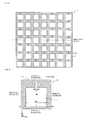
- Fig. 2 illustrates a periodic structure according to an embodiment of the present invention.
- the periodic structure shown in Fig. 2 includes rectangular aperture portions, each having a constricted portion (cutout portion) 11 a at one end thereof.
- the entire shape of an aperture portion 11, including the constricted portion 11 a is not mirror-symmetric with respect to an imaginary plane that is a plane perpendicular to the main surface of the periodic structure 1.
- the aperture portion 11 includes the constricted portion 11 a, at which the gap distance (the width in a direction parallel to the line of intersection of the main surface and the imaginary plane) of the aperture portion 11 is partially small.
- the periodic structure shown in Fig. 2 is a structure in which unit structures 10 having the aperture portions 11, one of which is shown in Fig. 3 , are periodically arranged and integrated with each other.
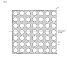
- Fig. 4 illustrates a periodic structure according to another embodiment of the present invention.
- the periodic structure shown in Fig. 4 includes circular aperture portions, each having a constricted portion (cutout portion) 11 a at one end thereof.
- the entire shape of an aperture portion 11, including the constricted portion 11 a is not mirror-symmetric with respect to an imaginary plane that is a plane perpendicular to the main surface of the periodic structure 1.
- the aperture portion 11 includes the constricted portion 11 a, at which the gap distance of the aperture portion 11 is partially small.
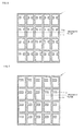
- Fig. 5 illustrates a periodic structure according to still another embodiment of the present invention.
- the periodic structure shown in Fig. 5 includes rectangular aperture portions, each having a slit portion (constricted portion) 11 a in a part thereof. It is necessary that the constricted portion 11 a is not mirror-symmetric with respect to an imaginary plane. Also in the present embodiment, the entire shape of an aperture portion 11, including the constricted portion 11 a, is not mirror-symmetric with respect to an imaginary plane that is a plane perpendicular to the main surface of the periodic structure 1. Moreover, the aperture portion 11 includes the constricted portion 11 a, at which the gap distance of the aperture portion 11 is partially small.
- the constricted portion 11 a may be formed so that the entire shape of the aperture portion 11 is mirror-symmetric with respect to a plane that is perpendicular to both the imaginary plane and the main surface of the periodic structure 1.
- the constricted portion 11 a may be formed so that the entire shape of the aperture portion 11 is not mirror-symmetric with respect a plane that is perpendicular to both the imaginary plane and the main surface of the periodic structure 1.
- the entire shape (external shape) of the periodic structure is not limited to square shapes shown in Figs. 2 to 6 . Any closed shape, such as a rectangular shape or a circular shape, may be used.
- the number of constricted portions (slits or cutout portions) in each aperture portion is not limited to one. Each aperture portion may have a plurality of constricted portions.
- a simulation calculation of the frequency characteristic of the electromagnetic wave transmittance of the periodic structure shown in Fig. 2 was performed. The calculation was performed for a unit structure of the periodic structure by using a periodic boundary condition.
- Fig. 3 is a front view of a unit structure of the periodic structure shown in Fig. 2 .
- One of the main surfaces of each unit structure 10 was used as an incident surface, the other main surface was used as a detection surface, and other surfaces were used as periodic boundaries (dotted lines).
- Design parameters shown in Fig. 3 were set as follows: P 260 ⁇ m, D2 180 ⁇ m, T (thickness) 60 ⁇ m, G 20 ⁇ m, and L 50 ⁇ m.
- the material of the periodic structure was Au.
- the unit structure was divided into unit cells each having dimensions of 5 ⁇ m in all of XYZ directions.
- a linearly polarized electromagnetic wave (plane wave) was emitted from a wave source 20 in a direction perpendicular to the main surface of the periodic structure 1, and the electromagnetic wave that had passed through the periodic structure 1 was detected by a detection surface 21 disposed opposite the wave source 20.
- the simulation calculation was performed for each of the following two cases: a case where a first electromagnetic wave (Y-polarized wave) polarized in a direction (Y-direction in Figs. 3 and 7 ) perpendicular to the imaginary plane shown in Fig. 2 was emitted; and a case where a second electromagnetic wave (Z-polarized wave) polarized in a direction (Z-direction in Figs. 3 and 7 ) parallel to the imaginary plane shown in Fig. 2 was emitted.
- the distance between the periodic structure 1 and the wave source 20 was 300 ⁇ m
- the distance between the periodic structure 1 and the detection surface 21 was 300 ⁇ m.
- Fig. 8 shows the frequency characteristics (transmittance spectra) of the transmittance of the periodic structure 1 obtained by the calculation.
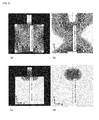
- Figs. 9(a) and 9(b) show a field intensity distribution that occurred when a periodic structure was irradiated with an electromagnetic wave having a frequency corresponding to a dip waveform of a Y-polarized wave in Fig. 8
- Figs. 9(c) and 9(d) show a field intensity distribution that occurred when the periodic structure was irradiated with an electromagnetic wave having a frequency corresponding to a dip waveform of a Z-polarized wave in Fig. 8
- Figs. 9(a) and 9(c) are views seen in the X-direction of Fig. 3
- Figs. 9(b) and 9(d) are views seen in the Z-direction of Fig. 3 .
- Fig. 10 shows a case where the periodic structure was irradiated with a Y-polarized wave (first electromagnetic wave)
- Fig. 11 shows a case where the periodic structure was irradiated with a Z-polarized wave (second electromagnetic wave).
- measurement using the periodic structure according to the present invention can be performed in both cases where the periodic structure is irradiated with electromagnetic waves having two different polarization directions.
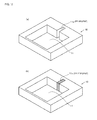
- Fig. 12 illustrate a periodic structure the same as that of Example 1 (periodic structure shown in Fig. 2 ) in a case where the cutout portion (constricted portion) 11 a of the aperture portion 11 is empty ( Fig. 12(a) ) and in a case where the constricted portion 11 a is filled with polyethylene.
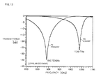
- Fig. 13 shows a change in the dip waveform of a transmittance spectrum obtained by using the periodic structure.
- Fig. 13 shows a case where the periodic structure was irradiated with a Z-polarized wave (second electromagnetic wave).
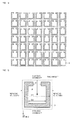
- Fig. 14 illustrates a periodic structure according to a Comparative Example, which has a structure in which independent slit ring resonators 3 are periodically arranged.
- Example 1 a simulation calculation of the frequency characteristic of electromagnetic wave transmittance was performed.
- Comparative Example 1 the calculation was performed for only the case where the periodic structure was irradiated with a Y-polarized wave (first electromagnetic wave).
- Fig. 15 is a front view of a unit structure of the periodic structure shown in Fig. 14 .
- One of the main surfaces of a slit ring resonator 3 was used as an incident surface, the other main surface was used as a detection surface, and periodic boundaries were set as shown by dotted lines in Fig. 14 .
- Design parameters shown in Fig. 14 were set as follows. G was set at 0 ⁇ m (in other words, simulation was performed on a ring resonator that did not have a slit). D1 was 260 ⁇ m, D2 was 180 ⁇ m, T (thickness) 60 ⁇ m; and P (pitch) was 280, 300, 340, and 420 ⁇ m.
- the material of the periodic structure was Au.
- the unit structure was divided into unit cells each having dimensions of 5 ⁇ m in all of XYZ directions.
- Fig. 16 shows transmittance spectra for the pitches obtained by calculation.
- a bandpass waveform having a passband near 1 THz was maintained.
- the bandpass waveform was considerably corrupted.
- the periodic structure shown in Fig. 2 was actually fabricated, and measurement of a transmittance spectrum was performed by using terahertz time-domain spectroscopy (THz-TDS).
- THz-TDS terahertz time-domain spectroscopy
- a process of fabricating the structure shown in Fig. 2 will be described below.
- a conductor plate having a smooth surface of a size 300 mm x 300 mm was prepared, and a photosensitive resin layer was formed on the surface so as to have a thickness of 100 ⁇ m.
- a photomask having a pattern of the periodic structure in the main surface shown in Fig. 2 was prepared, and portions corresponding to the aperture portions 11 shown in Fig. 2 were cured through UV radiation. Uncured resin portions were rinsed, and parts of the conductor plate excluding the portions corresponding to the aperture portions 11 of Fig. 2 were exposed.
- An extremely thin release layer was formed on the exposed parts of the conductor plate by applying a polymer solution to a surface that had been patterned by photolithography and drying the polymer solution.
- the conductor plate obtained as described above, was placed in a Ni-electroplating bath and an electric current was applied to the conductor plate, thereby forming an electroplated nickel layer having a thickness of 60 ⁇ m. After plating had been finished, cured resin remaining on the conductor plate was removed by using a solvent and the Ni plating structure was removed from the conductor plate, thereby obtaining a plate-shaped periodic structure made of Ni.
- Example 1 the obtained periodic structure was irradiated with each of a first electromagnetic wave (Y-polarized wave) and a second electromagnetic wave (Z-polarized wave), and the frequency characteristic of transmittance was measured by THz-TDS by using the apparatus shown in Fig. 1 .
- Fig. 17 shows the frequency characteristic of transmittance obtained when the periodic structure was irradiated with each of a first electromagnetic wave (Y-polarized wave) and a second electromagnetic wave (Z-polarized wave). It can be seen from the results shown in Fig. 17 that, for a periodic structure actually fabricated, the results the same as the simulation results of Example 1 shown in Fig. 8 were obtained.
- a polyethylene film having a thickness of 10 ⁇ m was prepared as an object.
- the film was affixed to one of the main surfaces of the periodic structure fabricated in Example 4, and the transmittance spectrum was measured in the same manner as in Example 4.
- Fig. 18 shows the frequency characteristic of transmittance obtained when the periodic structure was irradiated with each of a first electromagnetic wave (Y-polarized wave) and a second electromagnetic wave (Z-polarized wave).
- Y-polarized wave first electromagnetic wave
- Z-polarized wave second electromagnetic wave
- Example 4 By using the periodic structure fabricated in Example 4, an object was disposed only in the constricted portion 11 a and the transmittance spectrum of a Z-polarized wave (second electromagnetic wave) was measured.
- a surface of the periodic structure obtained in Example 4 was spin-coated with the photosensitive resin used in Example 4 (so that the constricted portion 11 a was also filled with the photosensitive resin). Then, a photomask for exposing only the cutout portions was prepared, the periodic structure was aligned, only the resin in the cutout portions was cured, and other unexposed portions ware rinsed, thereby obtaining a specimen in which the photosensitive resin remained only in the constricted portions (the constricted portions were filled with the photosensitive resin instead of PE in Fig. 9(b) ).
- the transmittance spectrum of a Z-polarized wave was measured as in Example 3 by using the periodic structure in which only the constricted portions were filled with the photosensitive resin.
- the transmittance spectrum of a Z-polarized wave was measured by using only the periodic structure that was obtained in Example 4 and that was not filled with the photosensitive resin.
- Fig. 19 shows the measurement results.
- a polyethylene film or a photosensitive resin was used as an object.
- a biomolecule such as a protein, a sugar chain, or DNA, or an inorganic compound may be used as an object.
- measurement was performed by directly attaching an object to the periodic structure.
- the molecules or the like may be fixed by means of specific adsorption using probe molecules, which are fixed to the periodic structure using a thiol group or a silane coupling group.
Landscapes
- Physics & Mathematics (AREA)
- Spectroscopy & Molecular Physics (AREA)
- Health & Medical Sciences (AREA)
- General Physics & Mathematics (AREA)
- Life Sciences & Earth Sciences (AREA)
- Chemical & Material Sciences (AREA)
- Analytical Chemistry (AREA)
- Biochemistry (AREA)
- General Health & Medical Sciences (AREA)
- Immunology (AREA)
- Pathology (AREA)
- Toxicology (AREA)
- Investigating Or Analysing Materials By Optical Means (AREA)
Applications Claiming Priority (2)
| Application Number | Priority Date | Filing Date | Title |
|---|---|---|---|
| JP2011252405 | 2011-11-18 | ||
| PCT/JP2012/070878 WO2013073242A1 (fr) | 2011-11-18 | 2012-08-17 | Structure périodique et procédé de mesure l'employant |
Publications (2)
| Publication Number | Publication Date |
|---|---|
| EP2781908A1 true EP2781908A1 (fr) | 2014-09-24 |
| EP2781908A4 EP2781908A4 (fr) | 2015-07-08 |
Family
ID=48429323
Family Applications (1)
| Application Number | Title | Priority Date | Filing Date |
|---|---|---|---|
| EP12850549.2A Withdrawn EP2781908A4 (fr) | 2011-11-18 | 2012-08-17 | Structure périodique et procédé de mesure l'employant |
Country Status (4)
| Country | Link |
|---|---|
| US (1) | US20140247452A1 (fr) |
| EP (1) | EP2781908A4 (fr) |
| JP (1) | JPWO2013073242A1 (fr) |
| WO (1) | WO2013073242A1 (fr) |
Families Citing this family (4)
| Publication number | Priority date | Publication date | Assignee | Title |
|---|---|---|---|---|
| JP6938291B2 (ja) * | 2017-09-08 | 2021-09-22 | 東芝テック株式会社 | センサ、検出装置及び検出システム |
| JP7181700B2 (ja) * | 2017-09-22 | 2022-12-01 | グローリー株式会社 | 電磁波検出装置、媒体処理装置及び媒体検査装置 |
| JP7208032B2 (ja) * | 2019-01-28 | 2023-01-18 | キヤノン株式会社 | 半導体装置 |
| JP7314026B2 (ja) * | 2019-11-14 | 2023-07-25 | 東芝テック株式会社 | 検出装置及び基板 |
Family Cites Families (5)
| Publication number | Priority date | Publication date | Assignee | Title |
|---|---|---|---|---|
| JP4911965B2 (ja) * | 2005-12-09 | 2012-04-04 | 株式会社アドバンテスト | 測定用構造体、測定装置、方法およびプログラム |
| DE102008016294A1 (de) * | 2008-03-28 | 2009-10-01 | Dritte Patentportfolio Beteiligungsgesellschaft Mbh & Co.Kg | Herstellungsverfahren für einen Oberflächensensor, System und Verwendung eines Oberflächensensors |
| JP5516589B2 (ja) * | 2009-09-03 | 2014-06-11 | 株式会社村田製作所 | 被測定物の特性を測定する方法、および測定システム |
| JP5218679B2 (ja) * | 2009-12-22 | 2013-06-26 | 株式会社村田製作所 | 被測定物の特性を測定する方法および測定装置 |
| WO2011142155A1 (fr) * | 2010-05-12 | 2011-11-17 | 株式会社村田製作所 | Procédé de mesure des caractéristiques d'un objet à mesurer, structure avec système de jour et dispositif de mesure utilisé à cette fin |
-
2012
- 2012-08-17 WO PCT/JP2012/070878 patent/WO2013073242A1/fr not_active Ceased
- 2012-08-17 EP EP12850549.2A patent/EP2781908A4/fr not_active Withdrawn
- 2012-08-17 JP JP2013544155A patent/JPWO2013073242A1/ja active Pending
-
2014
- 2014-05-15 US US14/278,593 patent/US20140247452A1/en not_active Abandoned
Also Published As
| Publication number | Publication date |
|---|---|
| EP2781908A4 (fr) | 2015-07-08 |
| WO2013073242A1 (fr) | 2013-05-23 |
| US20140247452A1 (en) | 2014-09-04 |
| JPWO2013073242A1 (ja) | 2015-04-02 |
Similar Documents
| Publication | Publication Date | Title |
|---|---|---|
| US8304732B2 (en) | Method of measuring characteristics of specimen and flat-plate periodic structure | |
| US8610071B2 (en) | Method of measuring characteristics of specimen, and flat-plate periodic structure | |
| JP5609654B2 (ja) | 被測定物の測定方法 | |
| US20140247452A1 (en) | Periodic structure and measurement method using the same | |
| JP5914474B2 (ja) | 被測定物の測定方法 | |
| US8912497B2 (en) | Measurement structure, method of manufacturing same, and measuring method using same | |
| US9075006B2 (en) | Measurement device and feature measurement method of object to be measured employing same | |
| US10408750B2 (en) | Void-arranged structure and measurement method using the same | |
| KR101672980B1 (ko) | 틈 배치 구조체 및 그것을 이용한 측정 방법 | |
| JPWO2011142155A1 (ja) | 被測定物の特性を測定する方法、それに用いられる空隙配置構造体および測定装置 | |
| JP5384648B2 (ja) | 被測定物の特性を測定する方法 | |
| EP2824435B1 (fr) | Détection de fréquence térahertz | |
| WO2012132982A1 (fr) | Dispositif de mesure, procédé de mesure utilisant un tel dispositif, et procédé pour la production de dispositif de mesure |
Legal Events
| Date | Code | Title | Description |
|---|---|---|---|
| PUAI | Public reference made under article 153(3) epc to a published international application that has entered the european phase |
Free format text: ORIGINAL CODE: 0009012 |
|
| 17P | Request for examination filed |
Effective date: 20140502 |
|
| AK | Designated contracting states |
Kind code of ref document: A1 Designated state(s): AL AT BE BG CH CY CZ DE DK EE ES FI FR GB GR HR HU IE IS IT LI LT LU LV MC MK MT NL NO PL PT RO RS SE SI SK SM TR |
|
| DAX | Request for extension of the european patent (deleted) | ||
| RA4 | Supplementary search report drawn up and despatched (corrected) |
Effective date: 20150610 |
|
| RIC1 | Information provided on ipc code assigned before grant |
Ipc: G01N 21/77 20060101ALI20150603BHEP Ipc: G01N 21/35 20140101AFI20150603BHEP |
|
| STAA | Information on the status of an ep patent application or granted ep patent |
Free format text: STATUS: THE APPLICATION IS DEEMED TO BE WITHDRAWN |
|
| 18D | Application deemed to be withdrawn |
Effective date: 20160108 |