EP2779811A1 - Drive circuit device - Google Patents
Drive circuit device Download PDFInfo
- Publication number
- EP2779811A1 EP2779811A1 EP14158022.5A EP14158022A EP2779811A1 EP 2779811 A1 EP2779811 A1 EP 2779811A1 EP 14158022 A EP14158022 A EP 14158022A EP 2779811 A1 EP2779811 A1 EP 2779811A1
- Authority
- EP
- European Patent Office
- Prior art keywords
- circuit
- heat
- circuit board
- switching elements
- drive circuit
- Prior art date
- Legal status (The legal status is an assumption and is not a legal conclusion. Google has not performed a legal analysis and makes no representation as to the accuracy of the status listed.)
- Withdrawn
Links
Images


Classifications
-
- H—ELECTRICITY
- H01—ELECTRIC ELEMENTS
- H01L—SEMICONDUCTOR DEVICES NOT COVERED BY CLASS H10
- H01L23/00—Details of semiconductor or other solid state devices
- H01L23/34—Arrangements for cooling, heating, ventilating or temperature compensation ; Temperature sensing arrangements
- H01L23/36—Selection of materials, or shaping, to facilitate cooling or heating, e.g. heatsinks
- H01L23/367—Cooling facilitated by shape of device
-
- H—ELECTRICITY
- H02—GENERATION; CONVERSION OR DISTRIBUTION OF ELECTRIC POWER
- H02M—APPARATUS FOR CONVERSION BETWEEN AC AND AC, BETWEEN AC AND DC, OR BETWEEN DC AND DC, AND FOR USE WITH MAINS OR SIMILAR POWER SUPPLY SYSTEMS; CONVERSION OF DC OR AC INPUT POWER INTO SURGE OUTPUT POWER; CONTROL OR REGULATION THEREOF
- H02M7/00—Conversion of ac power input into dc power output; Conversion of dc power input into ac power output
- H02M7/003—Constructional details, e.g. physical layout, assembly, wiring or busbar connections
-
- H—ELECTRICITY
- H05—ELECTRIC TECHNIQUES NOT OTHERWISE PROVIDED FOR
- H05K—PRINTED CIRCUITS; CASINGS OR CONSTRUCTIONAL DETAILS OF ELECTRIC APPARATUS; MANUFACTURE OF ASSEMBLAGES OF ELECTRICAL COMPONENTS
- H05K1/00—Printed circuits
- H05K1/02—Details
- H05K1/0213—Electrical arrangements not otherwise provided for
- H05K1/0263—High current adaptations, e.g. printed high current conductors or using auxiliary non-printed means; Fine and coarse circuit patterns on one circuit board
-
- H—ELECTRICITY
- H01—ELECTRIC ELEMENTS
- H01L—SEMICONDUCTOR DEVICES NOT COVERED BY CLASS H10
- H01L23/00—Details of semiconductor or other solid state devices
- H01L23/34—Arrangements for cooling, heating, ventilating or temperature compensation ; Temperature sensing arrangements
- H01L23/36—Selection of materials, or shaping, to facilitate cooling or heating, e.g. heatsinks
- H01L23/367—Cooling facilitated by shape of device
- H01L23/3675—Cooling facilitated by shape of device characterised by the shape of the housing
-
- H—ELECTRICITY
- H01—ELECTRIC ELEMENTS
- H01L—SEMICONDUCTOR DEVICES NOT COVERED BY CLASS H10
- H01L2924/00—Indexing scheme for arrangements or methods for connecting or disconnecting semiconductor or solid-state bodies as covered by H01L24/00
- H01L2924/0001—Technical content checked by a classifier
- H01L2924/0002—Not covered by any one of groups H01L24/00, H01L24/00 and H01L2224/00
-
- H—ELECTRICITY
- H05—ELECTRIC TECHNIQUES NOT OTHERWISE PROVIDED FOR
- H05K—PRINTED CIRCUITS; CASINGS OR CONSTRUCTIONAL DETAILS OF ELECTRIC APPARATUS; MANUFACTURE OF ASSEMBLAGES OF ELECTRICAL COMPONENTS
- H05K1/00—Printed circuits
- H05K1/02—Details
- H05K1/0201—Thermal arrangements, e.g. for cooling, heating or preventing overheating
- H05K1/0203—Cooling of mounted components
-
- H—ELECTRICITY
- H05—ELECTRIC TECHNIQUES NOT OTHERWISE PROVIDED FOR
- H05K—PRINTED CIRCUITS; CASINGS OR CONSTRUCTIONAL DETAILS OF ELECTRIC APPARATUS; MANUFACTURE OF ASSEMBLAGES OF ELECTRICAL COMPONENTS
- H05K2201/00—Indexing scheme relating to printed circuits covered by H05K1/00
- H05K2201/10—Details of components or other objects attached to or integrated in a printed circuit board
- H05K2201/10007—Types of components
- H05K2201/10166—Transistor
Definitions
- the present invention relates to a drive circuit device.
- a drive circuit which includes switching arms connected in parallel, is used to supply driving electric power to an electric motor.
- Each of the switching arms includes switching elements such as FETs connected in series.
- a drive circuit device motor control device
- a drive circuit device which is made small by using a circuit board having a multilayer structure, is known.
- the circuit board having the multilayer structure multiple circuit conductor layers, on which circuit patterns are formed, are stacked with insulating layers being interposed between the circuit conductor layers. For example, see Japanese Patent Application Publication No. 2009-277726 .
- switching elements are mounted on one surface of the circuit board and a heat-dissipating unit such as a heat sink is connected to the other surface of the circuit board so that heat is transferred to the heat sink. Accordingly, heat generated in the drive circuit (switching elements) is dissipated efficiently, and thus, the overheat of the drive circuit is prevented.
- An object of the invention is to provide a small-sized drive circuit device.
- a drive circuit device includes a circuit board in which a drive circuit is formed, the drive circuit including a plurality of switching arms connected in parallel, and each of the switching arms including a first switching element and a second switching element that are connected in series; and a heat-dissipating unit that dissipates heat of the circuit board to an outside
- the circuit board is a board having a multilayer structure in which multiple circuit conductor layers are stacked with insulating layers being interposed between the circuit conductor layers, the circuit conductor layers including circuit patterns made of a conductive material, wherein the first switching elements and the second switching elements are provided in the circuit board so that the circuit conductor layer is interposed between the first switching elements and the second switching elements, and a region in which the first switching elements are positioned and a region in which the second switching elements are positioned overlap each other in a stacking direction, and wherein a lead-out portion is formed at the circuit pattern of the circuit conductor layer interposed between the first switching elements and the second switching elements,
- the region in which the first switching elements are positioned and the region in which the second switching elements are positioned overlap each other in the stacking direction, and therefore, it is possible to reduce the size of the circuit board, as compared to a case where the first and second switching elements are mounted on one side surface of the circuit board.
- the lead-out portion is formed at the circuit pattern of the circuit conductor layer interposed between the first switching elements and the second switching elements, the lead-out portion extending to an area outside the circuit board, and being connected to the heat-dissipating unit so that heat is transferred to the heat-dissipating unit.
- the first switching elements and the second switching elements may be embedded in the circuit board, and the heat-dissipating units may be connected to the circuit board so that the circuit board is sandwiched from both sides in the stacking direction between the heat-dissipating units and heat is transferred to the heat-dissipating units.
- a drive circuit device 1 shown in FIG. 1 supplies driving electric power to an electric motor 2 used as a drive source of an electric power steering system that applies an assist force to a steering system.
- the drive circuit device 1 includes a drive circuit 3 that supplies driving electric power to the electric motor 2 and a control circuit 4 that controls the operation of the drive circuit 3.
- the drive circuit device 1 according to this embodiment is formed as a motor control device (an electronic control unit (ECU)).
- ECU electronic control unit
- a three-phase (a U phase, a V phase, and a W phase) brushless motor is employed as the electric motor 2 of this embodiment.
- the drive circuit 3 includes upper field-effect transistors (FETs) 12Hu, 12Hv, 12Hw that are connected to an in-vehicle power source (battery) 11, and lower FETs 12Lu, 12Lv, 12Lw that are connected to the ground.
- FETs field-effect transistors
- the upper FETs 12Hu, 12Hv, 12Hw serve as first switching elements
- the lower FETs 12Lu, 12Lv, 12Lw serve as second switching elements.
- the drive circuit 3 is formed by connecting, in parallel, a switching arm 13u including the upper FET 12Hu and the lower FET 12Lu that are connected in series, a switching arm 13v including the upper FET 12Hv and the lower FET 12Lv that are connected in series, and a switching arm 13w including the upper FET 12Hw and the lower FET 12Lw that are connected in series. That is, the drive circuit 3 is formed as a known pulse width modulation (PWM) inverter in which three switching arms 13u, 13v, 13w corresponding to motor coils 2u, 2v, 2w for the respective phases of the electric motor 2 are connected in parallel.
- PWM pulse width modulation
- drain electrodes de of the upper FETs 12Hu, 12Hv, 12Hw are connected to the in-vehicle power source 11 through power source (drain) lines 15u, 15v, 15w, respectively.
- Source electrodes se of the lower FETs 12Lu, 12Lv, 12Lw are connected to the ground through ground (source) lines 16u, 16v, 16w, respectively.
- Source electrodes se of the upper FETs 12Hu, 12Hv, 12Hw are connected to drain electrodes de of the lower FETs 12Lu, 12Lv, 12Lw through serial lines 17u, 17v, 17w, respectively.
- serial lines 17u, 17v, 17w are connected to the motor coils 2u, 2v, 2w for the respective phases through power lines 18u, 18v, 18w, respectively.
- Each of the upper FETs 12Hu, 12Hv, 12Hw and the lower FETs 12Lu, 12Lv, 12Lw is provided with a parasitic diode D that allows a current to flow toward the drain electrode de side from the source electrode se side.
- the control circuit 4 is connected to gate electrodes ge of the upper FETs 12Hu, 12Hv, 12Hw and the lower FETs 12Lu, 12Lv, 12Lw through signal (gate) lines 19u, 19v, 19w.
- a motor control signal is output to each of the gate electrodes ge, whereby the ON/OFF of each of the upper FETs 12Hu, 12Hv, 12Hw and the lower FETs 12Lu, 12Lv, 12Lw is controlled. That is, the motor control signal is a gate ON/OFF signal that defines the switching state of each of the upper FETs 12Hu, 12Hv, 12Hw and the lower FETs 12Lu, 12Lv, 12Lw.
- steering torque, vehicle speed, and the rotation angle of the electric motor 2 are input to the control circuit 4 of this embodiment. Accordingly, the control circuit 4 controls the operation of the electric motor 2 by outputting motor control signals based on these state quantities.
- the upper FETs 12Hu, 12Hv, 12Hw and the lower FETs 12Lu, 12Lv, 12Lw are turned on or off in response to the motor control signals, and accordingly, a current-supply pattern for the motor coils 2u, 2v, 2w for the respective phases is changed.
- a power supply voltage of the in-vehicle power source 11 is converted to three-phase driving electric power and the three-phase driving electric power is output to the electric motor 2.
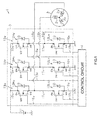
- the structure of a circuit board 21 on which the drive circuit 3 is formed will be described. Since the sectional structures of portions near the switching arms 13u, 13v, 13w in the drive circuit device 1 are the same, the structure of the switching arm 13u for a U phase will be described and the description of the switching arms 13v, 13w for a V phase and a W phase will be omitted for convenience of description.
- a board having a multilayer structure in which multiple circuit conductor layers are stacked with insulating layers being interposed between the circuit conductor layers, is used as the circuit board 21.
- Heat sinks 22, 23 as heat-dissipating units are connected to respective side surfaces of the circuit board 21 in a stacking direction (a top-bottom direction in FIG. 2 ) so that heat is transferred to the heat sinks 22, 23, and the circuit board 21 in this state is housed in a case 24 of the drive circuit device 1.
- the case 24 is formed in the shape of a quadrangular box.
- Each of the heat sinks 22, 23 is formed in the shape of a flat plate, and is fixed to the inner surface of the case 24.
- Each of the case 24 and the heat sinks 22, 23 is made of a material having high heat conductivity, such as an aluminum alloy.
- the circuit board 21 includes a first circuit conductor layer 31a, a second circuit conductor layer 31b, a third circuit conductor layer 31c, and a fourth circuit conductor layer 31d, and a first insulating layer 32a, a second insulating layer 32b, and a third insulating layer 32c that are interposed between these circuit conductor layers.
- the first circuit conductor layer 31a, the first insulating layer 32a, the second circuit conductor layer 31b, the second insulating layer 32b, the third circuit conductor layer 31c, the third insulating layer 32c, and the fourth circuit conductor layer 31d are stacked in this order from the heat sink 22 side (the lower side in FIG. 2 ).
- a sheet-shaped insulating member 25 is interposed between the first circuit conductor layer 31a and the heat sink 22 and another sheet-shaped insulating member 25 is interposed between the fourth circuit conductor layer 31d and the heat sink 23.
- the insulating member 25 of this embodiment is made of an insulating material having high heat conductivity, such as ceramics.
- the first circuit conductor layer 31a, the second circuit conductor layer 31b, the third circuit conductor layer 31c, and the fourth circuit conductor layer 31d include a first circuit pattern 33a, a second circuit pattern 33b, a third circuit pattern 33c, and a fourth circuit pattern 33d, respectively.
- Each of the first circuit pattern 33a, the second circuit pattern 33b, the third circuit pattern 33c, and the fourth circuit pattern 33d is formed by removing a part of conductive foil made of a conductive material such as copper foil. Gaps between lines forming the first circuit pattern 33a, the second circuit pattern 33b, the third circuit pattern 33c, and the fourth circuit pattern 33d are filled with an insulating resin material.
- the power source line 15u is included in the first circuit pattern 33a, the serial line 17u and the signal line 19u are included in the second circuit pattern 33b, and the ground line 16u and the signal line 19u are included in the third circuit pattern 33c.
- the first insulating layer 32a, the second insulating layer 32b, and the third insulating layer 32c are made of an insulating resin material, and thus, the first circuit pattern 33a, the second circuit pattern 33b, the third circuit pattern 33c, and the fourth circuit pattern 33d are insulated from each other.
- via holes (interlayer connection holes) 34 which extend through a predetermined circuit conductor layer and a predetermined insulating layer and extend in the stacking direction, are formed in the circuit board 21.
- Interlayer connection members 35 which are made of a conductor material such as copper, are inserted into the inner peripheries defining the via holes 34, and the circuit patterns of the different layers are electrically connected to each other through the interlayer connection members 35.
- the upper FET 12Hu in a bare chip state is embedded in the first insulating layer 32a, and the lower FET 12Lu in a bare chip state is embedded in the second insulating layer 32b. That is, the second circuit conductor layer 31b is interposed between the upper FET 12Hu and the lower FET 12Lu.
- the upper FET 12Hu and the lower FET 12Lu are disposed so that a region in which the upper FET 12Hu is positioned and a region in which the lower FET 12Lu is positioned overlap each other in the stacking direction.
- the drain electrode de of the upper FET 12Hu is electrically connected to the power source line 15u of the first circuit pattern 33a, the source electrode se thereof is electrically connected to the serial line 17u of the second circuit pattern 33b, and the gate electrode ge thereof is electrically connected to the signal line 19u of the second circuit pattern 33b.
- the drain electrode de of the lower FET 12Lu is electrically connected to the serial line 17u of the second circuit pattern 33b, the source electrode se thereof is electrically connected to the ground line 16u of the third circuit pattern 33c, and the gate electrode ge thereof is electrically connected to the signal line 19u of the third circuit pattern 33c. Accordingly, the switching arm 13u in which the upper FET 12Hu and the lower FET 12Lu are connected in series is formed.
- the second circuit conductor layer 31b is sandwiched from both sides in the stacking direction between the upper FET 12Hu and the lower FET 12Lu as described above. Accordingly, since both heat generated by the upper FET 12Hu and heat generated by the lower FET 12Lu are transferred to a portion of the second circuit conductor layer 31b, which is sandwiched between the upper FET 12Hu and the lower FET 12Lu, heat is likely to be accumulated at the above-mentioned portion of the second circuit conductor layer.
- a lead-out portion 41 which is continuous with the serial line 17u, extends in an orthogonal direction orthogonal to the stacking direction (a horizontal direction in FIG. 2 ), and extends to an area outside the circuit board 21, is formed at the second circuit pattern 33b to cope with the accumulation of heat.
- An extension portion 22a is formed at the heat sink 22 and an extension portion 23a is formed at the heat sink 23.
- Each of the extension portions 22a, 23a extends toward the lead-out portion 41-side in the stacking direction, from a portion protruding in the orthogonal direction beyond an edge portion of the circuit board 21.
- the lead-out portion 41 is connected to both the extension portions 22a, 23a with sheet-shaped insulating members 42 interposed therebetween so that heat is transferred to the extension portions 22a, 23a.
- a part of conductive foil formed on each side of an insulating layer which is to serve as one of the first insulating layer 32a, the second insulating layer 32b, and the third insulating layer 32c, is removed by etching or the like to form one of the first circuit pattern 33a, the second circuit pattern 33b, the third circuit pattern 33c, and the fourth circuit pattern 33d.
- a step of appropriately connecting the upper FETs 12Hu, 12Hv, 12Hw and the lower FETs 12Lu, 12Lv, 12Lw to the circuit pattern, stacking new conductive foil so that an insulating resin material forming an insulating layer is interposed between the circuit pattern and the conductive foil, and forming a circuit pattern on the conductive foil is repeated.
- the via holes 34 are formed and the interlayer connection members 35 are provided in the inner peripheries defining the via holes 34, and thus, the circuit board 21 is manufactured.
- each of the upper FETs 12Hu, 12Hv, 12Hw and the lower FETs 12Lu, 12Lv, 12Lw generates heat.
- heat generated by the upper FETs 12Hu, 12Hv, 12Hw is dissipated by being transferred to the heat sink 22 through the first circuit conductor layer 31a, and is dissipated by being transferred to the extension portions 22a, 23a of the heat sinks 22, 23 through the lead-out portion 41 of the second circuit conductor layer 31b.
- heat generated by the lower FETs 12Lu, 12Lv, 12Lw is dissipated by being transferred to the heat sink 23 through the third circuit conductor layer 31c, the third insulating layer 32c, the interlayer connection members 35, and the fourth circuit conductor layer 31d, and is dissipated by being transferred to the extension portions 22a, 23a of the heat sinks 22, 23 through the lead-out portion 41 of the second circuit conductor layer 31b. Accordingly, the heat of the entire circuit board 21 is efficiently dissipated.
- the lead-out portion 41 is formed at the second circuit pattern 33b and is connected to the extension portions 22a, 23a of the heat sinks 22, 23 so that heat is transferred to the extension portions 22a, 23a, heat of the portions of the second circuit conductor layer 31b, which are sandwiched from both sides in the stacking direction between the upper FETs 12Hu, 12Hv, 12Hw and the lower FETs 12Lu, 12Lv, 12Lw, can be efficiently dissipated through the lead-out portion 41. Accordingly, it is possible to reduce the size of the circuit board 21 while realizing high heat dissipation performance.
- Each of the upper FETs 12Hu, 12Hv, 12Hw and the lower FETs 12Lu, 12Lv, 12Lw in the bare chip state is embedded in the circuit board 21, and the heat sinks 22, 23 are connected to the circuit board 21 from both sides in the stacking direction so that the circuit board 21 is sandwiched from both sides in the stacking direction between the heat sinks 22, 23 and heat is transferred to the heat sinks 22, 23.
- the heat sinks 22, 23 are connected to the circuit board 21 from both sides in the stacking direction so that the circuit board 21 is sandwiched from both sides in the stacking direction between the heat sinks 22, 23 and heat is transferred to the heat sinks 22, 23.
- the invention may be implemented in the following modified examples obtained by appropriately modifying the above-mentioned embodiment.
- the heat sinks 22, 23 are formed in the shape of a flat plate in the above-mentioned embodiment, but the invention is not limited thereto.
- fins or the like may be formed on the side surface of each of the heat sinks 22, 23, the side surface being located on a side opposite to the circuit board 21-side.
- flow passages through which a refrigerant, such as water or air, passes may be formed in the heat sinks 22, 23.
- the heat sinks 22, 23 may not be separately provided and the circuit board 21 may be fixed to the inner surface of the case 24 so that the case 24 functions as a heat-dissipating unit.
- the lead-out portion 41 is connected to both the extension portions 22a, 23a so that heat is transferred to the extension portions 22a, 23a in the above-mentioned embodiment, but the invention is not limited thereto.
- the lead-out portion 41 may be connected to one of the extension portions 22a, 23a so that heat is transferred to the one of the extension portions 22a, 23a.
- the numbers of the circuit conductor layers and the insulating layers, the connection between the layers, or the like may be appropriately changed in the above-mentioned embodiment. Specifically, an insulating layer and a circuit conductor layer, which is connected to the first circuit conductor layer 31a through the interlayer connection members 35 (the via holes 34), may be added between the first circuit conductor layer 31a and the heat sink 22.
- the third circuit conductor layer 31c, to which the lower FET 12Lu is connected, may be connected to the heat sink 23 with the insulating member 25 interposed therebetween so that heat is transferred to the heat sink 23. Further, multiple circuit conductor layers may be interposed between the upper FET 12Hu and the lower FET 12Lu.
- the upper FETs 12Hu, 12Hv, 12Hw and the lower FETs 12Lu, 12Lv, 12Lw are embedded in the circuit board 21 in the above-mentioned embodiment, but the invention is not limited thereto.
- the upper FETs 12Hu, 12Hv, 12Hw and the lower FETs 12Lu, 12Lv, 12Lw may be provided so as to be exposed to the outside. In an embodiment shown in FIG.
- a lower FET 12Lu is provided so as to be exposed at the side surface of the circuit board 21, a bus bar 51 forming a ground line 16u is electrically connected to a source electrode se of the lower FET 12Lu, and a bus bar 52 forming a signal line 19u is electrically connected to a gate electrode ge of the lower FET 12Lu.
- a heat sink 23 be connected to the bus bars 51, 52 with an insulator 53 interposed therebetween so that heat is transferred to the bus bars 51, 52 as shown in FIG. 3 .
- the drive circuit 3 is formed using FETs in the above-mentioned embodiment, but the invention is not limited thereto.
- the drive circuit 3 may be formed using other switching elements such as insulated gate bipolar transistors (IGBTs).
- IGBTs insulated gate bipolar transistors
- the diodes are used in combination. Specifically, as shown in FIG. 4 , a collector electrode coe of an upper IGBT 55Hu and a cathode electrode cae of an upper diode 56Hu are electrically connected to a power source line 15u of a first circuit pattern 33a.
- An emitter electrode ee of the upper IGBT 55Hu, an anode electrode ae of the upper diode 56Hu, and a collector electrode coe of a lower IGBT 55Lu, and a cathode electrode cae of a lower diode 56Lu are electrically connected to a serial line 17u of a second circuit pattern 33b.
- An emitter electrode ee of the lower IGBT 55Lu and an anode electrode ae of the lower diode 56Lu are electrically connected to a ground line 16u of a third circuit pattern 33c.
- a gate electrode ge of the upper IGBT 55Hu is connected to a signal line 19u of the second circuit pattern 33b, and a gate electrode ge of the lower IGBT 55Lu is connected to a signal line 19u of the third circuit pattern 33c.
- the drive circuit device 1 includes the control circuit in the above-mentioned embodiment, but the invention is not limited thereto.
- a control circuit device including a control circuit may be separately provided, and the drive circuit device 1 may not include a control circuit.
- a brushless motor is used as the electric motor 2 in the above-mentioned embodiment, but the prevent invention is not limited thereto.
- a DC motor with a brush may be used as the electric motor 2.
- the drive circuit 3 is formed as an H bridge circuit in which two switching arms are connected in parallel.
- Driving electric power is supplied to the electric motor 2 that applies an assist force, by using the drive circuit device 1 in the above-mentioned embodiment, but the invention is not limited thereto.
- driving electric power may be supplied to an electric motor used as a drive source of another device such as an electric pump device.
- Each of the switching elements in the bare chip state is embedded in the circuit board. According to the above-mentioned structure, it is possible to make the circuit board smaller.
Landscapes
- Engineering & Computer Science (AREA)
- Microelectronics & Electronic Packaging (AREA)
- Power Engineering (AREA)
- Physics & Mathematics (AREA)
- Computer Hardware Design (AREA)
- General Physics & Mathematics (AREA)
- Chemical & Material Sciences (AREA)
- Condensed Matter Physics & Semiconductors (AREA)
- Materials Engineering (AREA)
- Inverter Devices (AREA)
- Structure Of Printed Boards (AREA)
- Power Steering Mechanism (AREA)
- Thermal Sciences (AREA)
Abstract
Description
- The present invention relates to a drive circuit device.
- In general, a drive circuit (inverter), which includes switching arms connected in parallel, is used to supply driving electric power to an electric motor. Each of the switching arms includes switching elements such as FETs connected in series. As a conventional drive circuit device (motor control device) including the drive circuit, a drive circuit device, which is made small by using a circuit board having a multilayer structure, is known. In the circuit board having the multilayer structure, multiple circuit conductor layers, on which circuit patterns are formed, are stacked with insulating layers being interposed between the circuit conductor layers. For example, see Japanese Patent Application Publication No.
2009-277726 - Since a large drive current for driving the electric motor flows in the drive circuit, the amount of heat generated in the drive circuit is increased, and thus, the drive circuit is likely to be overheated. In the drive circuit device described in Japanese Patent Application Publication No.
2009-277726 - In recent years, the further reduction of the size of the drive circuit device has been required. However, since a mounting area needs to be secured on the circuit board in the structure in which the switching elements are mounted on one surface of the circuit board as described in Japanese Patent Application Publication No.
2009-277726 - An object of the invention is to provide a small-sized drive circuit device.
- A drive circuit device according to an aspect of the invention includes a circuit board in which a drive circuit is formed, the drive circuit including a plurality of switching arms connected in parallel, and each of the switching arms including a first switching element and a second switching element that are connected in series; and a heat-dissipating unit that dissipates heat of the circuit board to an outside, wherein the circuit board is a board having a multilayer structure in which multiple circuit conductor layers are stacked with insulating layers being interposed between the circuit conductor layers, the circuit conductor layers including circuit patterns made of a conductive material, wherein the first switching elements and the second switching elements are provided in the circuit board so that the circuit conductor layer is interposed between the first switching elements and the second switching elements, and a region in which the first switching elements are positioned and a region in which the second switching elements are positioned overlap each other in a stacking direction, and wherein a lead-out portion is formed at the circuit pattern of the circuit conductor layer interposed between the first switching elements and the second switching elements, the lead-out portion extending from the circuit board in a direction orthogonal to the stacking direction, and being connected to the heat-dissipating unit so that heat is transferred to the heat-dissipating unit.
- With the structure according to the above-mentioned aspect, the region in which the first switching elements are positioned and the region in which the second switching elements are positioned overlap each other in the stacking direction, and therefore, it is possible to reduce the size of the circuit board, as compared to a case where the first and second switching elements are mounted on one side surface of the circuit board.
- In the above-mentioned structure, in the circuit board, there are portions sandwiched from both sides in the stacking direction between the first switching elements and the second switching elements. Since both heat generated by the first switching elements and heat generated by the second switching elements are transferred to the portions, heat is likely to be accumulated at the portions. In the above-mentioned structure, the lead-out portion is formed at the circuit pattern of the circuit conductor layer interposed between the first switching elements and the second switching elements, the lead-out portion extending to an area outside the circuit board, and being connected to the heat-dissipating unit so that heat is transferred to the heat-dissipating unit. Therefore, it is possible to efficiently dissipate heat of the portions that are sandwiched from both sides in the stacking direction between the first switching elements and the second switching elements, through the lead-out portion of the circuit pattern. Thus, it is possible to reduce the size of the circuit board, while realizing high heat dissipation performance.
- In the drive circuit device according to the above-mentioned aspect, the first switching elements and the second switching elements may be embedded in the circuit board, and the heat-dissipating units may be connected to the circuit board so that the circuit board is sandwiched from both sides in the stacking direction between the heat-dissipating units and heat is transferred to the heat-dissipating units.
- With the above-mentioned structure, it is possible to efficiently dissipate heat toward areas on both sides of the circuit board in the stacking direction, through the heat-dissipating units, and accordingly, it is possible to realize higher heat dissipation performance.
- The foregoing and further features and advantages of the invention will become apparent from the following description of example embodiments with reference to the accompanying drawings, wherein like numerals are used to represent like elements and wherein:
-
FIG. 1 is a block diagram schematically illustrating a drive circuit device; -
FIG. 2 is a partial sectional view illustrating a drive circuit device according to an embodiment; -
FIG. 3 is a partial sectional view illustrating a drive circuit device according to a modified example; and -
FIG. 4 is a partial sectional view illustrating a drive circuit device according to another modified example. - An embodiment of the invention will be described below with reference to the drawings. A
drive circuit device 1 shown inFIG. 1 supplies driving electric power to anelectric motor 2 used as a drive source of an electric power steering system that applies an assist force to a steering system. As shown inFIG. 1 , thedrive circuit device 1 includes adrive circuit 3 that supplies driving electric power to theelectric motor 2 and acontrol circuit 4 that controls the operation of thedrive circuit 3. Thedrive circuit device 1 according to this embodiment is formed as a motor control device (an electronic control unit (ECU)). A three-phase (a U phase, a V phase, and a W phase) brushless motor is employed as theelectric motor 2 of this embodiment. - The
drive circuit 3 includes upper field-effect transistors (FETs) 12Hu, 12Hv, 12Hw that are connected to an in-vehicle power source (battery) 11, and lower FETs 12Lu, 12Lv, 12Lw that are connected to the ground. The upper FETs 12Hu, 12Hv, 12Hw serve as first switching elements, and the lower FETs 12Lu, 12Lv, 12Lw serve as second switching elements. Thedrive circuit 3 is formed by connecting, in parallel, a switchingarm 13u including the upper FET 12Hu and the lower FET 12Lu that are connected in series, aswitching arm 13v including the upper FET 12Hv and the lower FET 12Lv that are connected in series, and aswitching arm 13w including the upper FET 12Hw and the lower FET 12Lw that are connected in series. That is, thedrive circuit 3 is formed as a known pulse width modulation (PWM) inverter in which three switchingarms motor coils electric motor 2 are connected in parallel. - More specifically, drain electrodes de of the upper FETs 12Hu, 12Hv, 12Hw are connected to the in-
vehicle power source 11 through power source (drain)lines lines serial lines 17u, 17v, 17w, respectively. Theserial lines 17u, 17v, 17w are connected to themotor coils power lines - The
control circuit 4 is connected to gate electrodes ge of the upper FETs 12Hu, 12Hv, 12Hw and the lower FETs 12Lu, 12Lv, 12Lw through signal (gate)lines electric motor 2 are input to thecontrol circuit 4 of this embodiment. Accordingly, thecontrol circuit 4 controls the operation of theelectric motor 2 by outputting motor control signals based on these state quantities. - In the
drive circuit device 1 that is formed in this manner, the upper FETs 12Hu, 12Hv, 12Hw and the lower FETs 12Lu, 12Lv, 12Lw are turned on or off in response to the motor control signals, and accordingly, a current-supply pattern for themotor coils vehicle power source 11 is converted to three-phase driving electric power and the three-phase driving electric power is output to theelectric motor 2. - The structure of a
circuit board 21 on which thedrive circuit 3 is formed will be described. Since the sectional structures of portions near the switchingarms drive circuit device 1 are the same, the structure of theswitching arm 13u for a U phase will be described and the description of the switchingarms - As shown in
FIG. 2 , a board having a multilayer structure, in which multiple circuit conductor layers are stacked with insulating layers being interposed between the circuit conductor layers, is used as thecircuit board 21. Heat sinks 22, 23 as heat-dissipating units are connected to respective side surfaces of thecircuit board 21 in a stacking direction (a top-bottom direction inFIG. 2 ) so that heat is transferred to theheat sinks circuit board 21 in this state is housed in acase 24 of thedrive circuit device 1. - More specifically, the
case 24 is formed in the shape of a quadrangular box. Each of the heat sinks 22, 23 is formed in the shape of a flat plate, and is fixed to the inner surface of thecase 24. Each of thecase 24 and the heat sinks 22, 23 is made of a material having high heat conductivity, such as an aluminum alloy. - The
circuit board 21 includes a firstcircuit conductor layer 31a, a secondcircuit conductor layer 31b, a thirdcircuit conductor layer 31c, and a fourthcircuit conductor layer 31d, and afirst insulating layer 32a, a secondinsulating layer 32b, and a thirdinsulating layer 32c that are interposed between these circuit conductor layers. In this embodiment, the firstcircuit conductor layer 31a, thefirst insulating layer 32a, the secondcircuit conductor layer 31b, the secondinsulating layer 32b, the thirdcircuit conductor layer 31c, the thirdinsulating layer 32c, and the fourthcircuit conductor layer 31d are stacked in this order from theheat sink 22 side (the lower side inFIG. 2 ). Further, a sheet-shaped insulating member 25 is interposed between the firstcircuit conductor layer 31a and theheat sink 22 and another sheet-shaped insulating member 25 is interposed between the fourthcircuit conductor layer 31d and theheat sink 23. The insulatingmember 25 of this embodiment is made of an insulating material having high heat conductivity, such as ceramics. - The first
circuit conductor layer 31a, the secondcircuit conductor layer 31b, the thirdcircuit conductor layer 31c, and the fourthcircuit conductor layer 31d include afirst circuit pattern 33a, asecond circuit pattern 33b, athird circuit pattern 33c, and afourth circuit pattern 33d, respectively. Each of thefirst circuit pattern 33a, thesecond circuit pattern 33b, thethird circuit pattern 33c, and thefourth circuit pattern 33d is formed by removing a part of conductive foil made of a conductive material such as copper foil. Gaps between lines forming thefirst circuit pattern 33a, thesecond circuit pattern 33b, thethird circuit pattern 33c, and thefourth circuit pattern 33d are filled with an insulating resin material. Thepower source line 15u is included in thefirst circuit pattern 33a, theserial line 17u and thesignal line 19u are included in thesecond circuit pattern 33b, and theground line 16u and thesignal line 19u are included in thethird circuit pattern 33c. - The first insulating
layer 32a, the second insulatinglayer 32b, and the third insulatinglayer 32c are made of an insulating resin material, and thus, thefirst circuit pattern 33a, thesecond circuit pattern 33b, thethird circuit pattern 33c, and thefourth circuit pattern 33d are insulated from each other. Further, via holes (interlayer connection holes) 34, which extend through a predetermined circuit conductor layer and a predetermined insulating layer and extend in the stacking direction, are formed in thecircuit board 21.Interlayer connection members 35, which are made of a conductor material such as copper, are inserted into the inner peripheries defining the via holes 34, and the circuit patterns of the different layers are electrically connected to each other through theinterlayer connection members 35. - The upper FET 12Hu in a bare chip state is embedded in the first insulating
layer 32a, and the lower FET 12Lu in a bare chip state is embedded in the second insulatinglayer 32b. That is, the secondcircuit conductor layer 31b is interposed between the upper FET 12Hu and the lower FET 12Lu. The upper FET 12Hu and the lower FET 12Lu are disposed so that a region in which the upper FET 12Hu is positioned and a region in which the lower FET 12Lu is positioned overlap each other in the stacking direction. - The drain electrode de of the upper FET 12Hu is electrically connected to the
power source line 15u of thefirst circuit pattern 33a, the source electrode se thereof is electrically connected to theserial line 17u of thesecond circuit pattern 33b, and the gate electrode ge thereof is electrically connected to thesignal line 19u of thesecond circuit pattern 33b. The drain electrode de of the lower FET 12Lu is electrically connected to theserial line 17u of thesecond circuit pattern 33b, the source electrode se thereof is electrically connected to theground line 16u of thethird circuit pattern 33c, and the gate electrode ge thereof is electrically connected to thesignal line 19u of thethird circuit pattern 33c. Accordingly, theswitching arm 13u in which the upper FET 12Hu and the lower FET 12Lu are connected in series is formed. - In this embodiment, the second
circuit conductor layer 31b is sandwiched from both sides in the stacking direction between the upper FET 12Hu and the lower FET 12Lu as described above. Accordingly, since both heat generated by the upper FET 12Hu and heat generated by the lower FET 12Lu are transferred to a portion of the secondcircuit conductor layer 31b, which is sandwiched between the upper FET 12Hu and the lower FET 12Lu, heat is likely to be accumulated at the above-mentioned portion of the second circuit conductor layer. - A lead-out
portion 41, which is continuous with theserial line 17u, extends in an orthogonal direction orthogonal to the stacking direction (a horizontal direction inFIG. 2 ), and extends to an area outside thecircuit board 21, is formed at thesecond circuit pattern 33b to cope with the accumulation of heat. Anextension portion 22a is formed at theheat sink 22 and anextension portion 23a is formed at theheat sink 23. Each of theextension portions circuit board 21. The lead-outportion 41 is connected to both theextension portions members 42 interposed therebetween so that heat is transferred to theextension portions - In the manufacture of the
circuit board 21, first, a part of conductive foil formed on each side of an insulating layer, which is to serve as one of the first insulatinglayer 32a, the second insulatinglayer 32b, and the third insulatinglayer 32c, is removed by etching or the like to form one of thefirst circuit pattern 33a, thesecond circuit pattern 33b, thethird circuit pattern 33c, and thefourth circuit pattern 33d. Subsequently, a step of appropriately connecting the upper FETs 12Hu, 12Hv, 12Hw and the lower FETs 12Lu, 12Lv, 12Lw to the circuit pattern, stacking new conductive foil so that an insulating resin material forming an insulating layer is interposed between the circuit pattern and the conductive foil, and forming a circuit pattern on the conductive foil is repeated. Then, the via holes 34 are formed and theinterlayer connection members 35 are provided in the inner peripheries defining the via holes 34, and thus, thecircuit board 21 is manufactured. - The action of this embodiment will be described. When driving electric power is supplied to the
electric motor 2, each of the upper FETs 12Hu, 12Hv, 12Hw and the lower FETs 12Lu, 12Lv, 12Lw generates heat. At this time, heat generated by the upper FETs 12Hu, 12Hv, 12Hw is dissipated by being transferred to theheat sink 22 through the firstcircuit conductor layer 31a, and is dissipated by being transferred to theextension portions portion 41 of the secondcircuit conductor layer 31b. On the other hand, heat generated by the lower FETs 12Lu, 12Lv, 12Lw is dissipated by being transferred to theheat sink 23 through the thirdcircuit conductor layer 31c, the third insulatinglayer 32c, theinterlayer connection members 35, and the fourthcircuit conductor layer 31d, and is dissipated by being transferred to theextension portions portion 41 of the secondcircuit conductor layer 31b. Accordingly, the heat of theentire circuit board 21 is efficiently dissipated. - Next, the effects of this embodiment will be described. Since the regions in which the upper FETs 12Hu, 12Hv, 12Hw are positioned and the regions in which the lower FETs 12Lu, 12Lv, 12Lw are positioned overlap each other in the stacking direction, the area of the
circuit board 21 can be reduced. Further, since the lead-outportion 41 is formed at thesecond circuit pattern 33b and is connected to theextension portions extension portions circuit conductor layer 31b, which are sandwiched from both sides in the stacking direction between the upper FETs 12Hu, 12Hv, 12Hw and the lower FETs 12Lu, 12Lv, 12Lw, can be efficiently dissipated through the lead-outportion 41. Accordingly, it is possible to reduce the size of thecircuit board 21 while realizing high heat dissipation performance. - Each of the upper FETs 12Hu, 12Hv, 12Hw and the lower FETs 12Lu, 12Lv, 12Lw in the bare chip state is embedded in the
circuit board 21, and the heat sinks 22, 23 are connected to thecircuit board 21 from both sides in the stacking direction so that thecircuit board 21 is sandwiched from both sides in the stacking direction between the heat sinks 22, 23 and heat is transferred to the heat sinks 22, 23. Thus, it is possible to efficiently dissipate heat toward areas on both sides of thecircuit board 21 in the stacking direction through the heat sinks 22, 23, to realize higher heat dissipation performance, and to reduce the size of thecircuit board 21. - The invention may be implemented in the following modified examples obtained by appropriately modifying the above-mentioned embodiment. The heat sinks 22, 23 are formed in the shape of a flat plate in the above-mentioned embodiment, but the invention is not limited thereto. For example, fins or the like may be formed on the side surface of each of the heat sinks 22, 23, the side surface being located on a side opposite to the circuit board 21-side. Further, flow passages through which a refrigerant, such as water or air, passes may be formed in the heat sinks 22, 23. Furthermore, the heat sinks 22, 23 may not be separately provided and the
circuit board 21 may be fixed to the inner surface of thecase 24 so that thecase 24 functions as a heat-dissipating unit. - The lead-out
portion 41 is connected to both theextension portions extension portions portion 41 may be connected to one of theextension portions extension portions - The numbers of the circuit conductor layers and the insulating layers, the connection between the layers, or the like may be appropriately changed in the above-mentioned embodiment. Specifically, an insulating layer and a circuit conductor layer, which is connected to the first
circuit conductor layer 31a through the interlayer connection members 35 (the via holes 34), may be added between the firstcircuit conductor layer 31a and theheat sink 22. The thirdcircuit conductor layer 31c, to which the lower FET 12Lu is connected, may be connected to theheat sink 23 with the insulatingmember 25 interposed therebetween so that heat is transferred to theheat sink 23. Further, multiple circuit conductor layers may be interposed between the upper FET 12Hu and the lower FET 12Lu. - The upper FETs 12Hu, 12Hv, 12Hw and the lower FETs 12Lu, 12Lv, 12Lw are embedded in the
circuit board 21 in the above-mentioned embodiment, but the invention is not limited thereto. The upper FETs 12Hu, 12Hv, 12Hw and the lower FETs 12Lu, 12Lv, 12Lw may be provided so as to be exposed to the outside. In an embodiment shown inFIG. 3 , a lower FET 12Lu is provided so as to be exposed at the side surface of thecircuit board 21, abus bar 51 forming aground line 16u is electrically connected to a source electrode se of the lower FET 12Lu, and abus bar 52 forming asignal line 19u is electrically connected to a gate electrode ge of the lower FET 12Lu. In this case, it is preferable that aheat sink 23 be connected to the bus bars 51, 52 with aninsulator 53 interposed therebetween so that heat is transferred to the bus bars 51, 52 as shown inFIG. 3 . - The
drive circuit 3 is formed using FETs in the above-mentioned embodiment, but the invention is not limited thereto. For example, thedrive circuit 3 may be formed using other switching elements such as insulated gate bipolar transistors (IGBTs). In the structure using IGBTs, the diodes are used in combination. Specifically, as shown inFIG. 4 , a collector electrode coe of an upper IGBT 55Hu and a cathode electrode cae of an upper diode 56Hu are electrically connected to apower source line 15u of afirst circuit pattern 33a. An emitter electrode ee of the upper IGBT 55Hu, an anode electrode ae of the upper diode 56Hu, and a collector electrode coe of a lower IGBT 55Lu, and a cathode electrode cae of a lower diode 56Lu are electrically connected to aserial line 17u of asecond circuit pattern 33b. An emitter electrode ee of the lower IGBT 55Lu and an anode electrode ae of the lower diode 56Lu are electrically connected to aground line 16u of athird circuit pattern 33c. A gate electrode ge of the upper IGBT 55Hu is connected to asignal line 19u of thesecond circuit pattern 33b, and a gate electrode ge of the lower IGBT 55Lu is connected to asignal line 19u of thethird circuit pattern 33c. - An FET or the like in which a bare chip is sealed (packaged) with a sealant or the like may be used as the switching element in the above-mentioned embodiment. The
drive circuit device 1 includes the control circuit in the above-mentioned embodiment, but the invention is not limited thereto. A control circuit device including a control circuit may be separately provided, and thedrive circuit device 1 may not include a control circuit. - A brushless motor is used as the
electric motor 2 in the above-mentioned embodiment, but the prevent invention is not limited thereto. For example, a DC motor with a brush may be used as theelectric motor 2. In this case, thedrive circuit 3 is formed as an H bridge circuit in which two switching arms are connected in parallel. - Driving electric power is supplied to the
electric motor 2 that applies an assist force, by using thedrive circuit device 1 in the above-mentioned embodiment, but the invention is not limited thereto. For example, driving electric power may be supplied to an electric motor used as a drive source of another device such as an electric pump device. - Next, the technical idea, which can be understood from the above-mentioned embodiment and modified examples, will be additionally described below together with the effects thereof. Each of the switching elements in the bare chip state is embedded in the circuit board. According to the above-mentioned structure, it is possible to make the circuit board smaller.
Claims (2)
- A drive circuit device comprising:a circuit board in which a drive circuit is formed, the drive circuit including a plurality of switching arms connected in parallel, and each of the switching arms including a first switching element and a second switching element that are connected in series; anda heat-dissipating unit that dissipates heat of the circuit board to an outside,wherein the circuit board is a board having a multilayer structure in which multiple circuit conductor layers are stacked with insulating layers being interposed between the circuit conductor layers, the circuit conductor layers including circuit patterns made of a conductive material,wherein the first switching elements and the second switching elements are provided in the circuit board so that the circuit conductor layer is interposed between the first switching elements and the second switching elements, and a region in which the first switching elements are positioned and a region in which the second switching elements are positioned overlap each other in a stacking direction, andwherein a lead-out portion is formed at the circuit pattern of the circuit conductor layer interposed between the first switching elements and the second switching elements, the lead-out portion extending from the circuit board in a direction orthogonal to the stacking direction, and being connected to the heat-dissipating unit so that heat is transferred to the heat-dissipating unit.
- The drive circuit device according to claim 1, wherein
the first switching elements and the second switching elements are embedded in the circuit board, and
the heat-dissipating units are connected to the circuit board so that the circuit board is sandwiched from both sides in the stacking direction between the heat-dissipating units and heat is transferred to the heat-dissipating units.
Applications Claiming Priority (1)
| Application Number | Priority Date | Filing Date | Title |
|---|---|---|---|
| JP2013047828A JP6075128B2 (en) | 2013-03-11 | 2013-03-11 | Drive circuit device |
Publications (1)
| Publication Number | Publication Date |
|---|---|
| EP2779811A1 true EP2779811A1 (en) | 2014-09-17 |
Family
ID=50193371
Family Applications (1)
| Application Number | Title | Priority Date | Filing Date |
|---|---|---|---|
| EP14158022.5A Withdrawn EP2779811A1 (en) | 2013-03-11 | 2014-03-06 | Drive circuit device |
Country Status (4)
| Country | Link |
|---|---|
| US (1) | US9373560B2 (en) |
| EP (1) | EP2779811A1 (en) |
| JP (1) | JP6075128B2 (en) |
| CN (1) | CN104052308B (en) |
Families Citing this family (4)
| Publication number | Priority date | Publication date | Assignee | Title |
|---|---|---|---|---|
| JP6115465B2 (en) * | 2013-12-26 | 2017-04-19 | 株式会社デンソー | Electronic control unit and electric power steering apparatus using the same |
| JP6771447B2 (en) * | 2017-09-29 | 2020-10-21 | 日立オートモティブシステムズ株式会社 | Power semiconductor device and power conversion device using it |
| JP7406931B2 (en) * | 2019-07-11 | 2023-12-28 | 株式会社マキタ | electric work equipment |
| US11037853B1 (en) * | 2019-12-17 | 2021-06-15 | Advanced Semiconductor Engineering, Inc. | Semiconductor package structure and method of manufacturing the same |
Citations (4)
| Publication number | Priority date | Publication date | Assignee | Title |
|---|---|---|---|---|
| EP2066158A2 (en) * | 2007-11-30 | 2009-06-03 | Itt Manufacturing Enterprises, Inc. | Multilayer, thermally-stabilized substrate structures |
| JP2009277726A (en) | 2008-05-12 | 2009-11-26 | Jtekt Corp | Laminated circuit board, motor controller and steering device for vehicle |
| DE102008040906A1 (en) * | 2008-07-31 | 2010-02-04 | Robert Bosch Gmbh | Printed circuit board with electronic component |
| US20120106220A1 (en) * | 2010-11-03 | 2012-05-03 | Denso Corporation | Switching module |
Family Cites Families (10)
| Publication number | Priority date | Publication date | Assignee | Title |
|---|---|---|---|---|
| DE19726534A1 (en) * | 1997-06-23 | 1998-12-24 | Asea Brown Boveri | Power semiconductor module with closed submodules |
| JP3673776B2 (en) * | 2002-07-03 | 2005-07-20 | 株式会社日立製作所 | Semiconductor module and power conversion device |
| US7327024B2 (en) * | 2004-11-24 | 2008-02-05 | General Electric Company | Power module, and phase leg assembly |
| JP4446964B2 (en) * | 2006-01-11 | 2010-04-07 | 三菱電機株式会社 | Induction heating cooker |
| JP4930231B2 (en) * | 2006-07-20 | 2012-05-16 | セイコーエプソン株式会社 | Liquid ejector |
| JP4909712B2 (en) * | 2006-11-13 | 2012-04-04 | 日立オートモティブシステムズ株式会社 | Power converter |
| JP5326269B2 (en) * | 2006-12-18 | 2013-10-30 | 大日本印刷株式会社 | Electronic component built-in wiring board, and heat dissipation method for electronic component built-in wiring board |
| JP5444619B2 (en) * | 2008-02-07 | 2014-03-19 | 株式会社ジェイテクト | Multi-layer circuit board and motor drive circuit board |
| JP5067267B2 (en) * | 2008-06-05 | 2012-11-07 | 三菱電機株式会社 | Resin-sealed semiconductor device and manufacturing method thereof |
| CN102339818B (en) * | 2010-07-15 | 2014-04-30 | 台达电子工业股份有限公司 | Power module and manufacture method thereof |
-
2013
- 2013-03-11 JP JP2013047828A patent/JP6075128B2/en not_active Expired - Fee Related
-
2014
- 2014-03-04 US US14/195,975 patent/US9373560B2/en not_active Expired - Fee Related
- 2014-03-04 CN CN201410076814.3A patent/CN104052308B/en not_active Expired - Fee Related
- 2014-03-06 EP EP14158022.5A patent/EP2779811A1/en not_active Withdrawn
Patent Citations (4)
| Publication number | Priority date | Publication date | Assignee | Title |
|---|---|---|---|---|
| EP2066158A2 (en) * | 2007-11-30 | 2009-06-03 | Itt Manufacturing Enterprises, Inc. | Multilayer, thermally-stabilized substrate structures |
| JP2009277726A (en) | 2008-05-12 | 2009-11-26 | Jtekt Corp | Laminated circuit board, motor controller and steering device for vehicle |
| DE102008040906A1 (en) * | 2008-07-31 | 2010-02-04 | Robert Bosch Gmbh | Printed circuit board with electronic component |
| US20120106220A1 (en) * | 2010-11-03 | 2012-05-03 | Denso Corporation | Switching module |
Also Published As
| Publication number | Publication date |
|---|---|
| JP6075128B2 (en) | 2017-02-08 |
| US20140254105A1 (en) | 2014-09-11 |
| CN104052308A (en) | 2014-09-17 |
| JP2014176225A (en) | 2014-09-22 |
| US9373560B2 (en) | 2016-06-21 |
| CN104052308B (en) | 2018-05-29 |
Similar Documents
| Publication | Publication Date | Title |
|---|---|---|
| US8705257B2 (en) | Switching module including a snubber circuit connected in parallel to a series-connected unit of flowing restriction elements | |
| US8564996B2 (en) | Semiconductor module and driving apparatus including semiconductor module | |
| US9870984B2 (en) | Power field-effect transistor (FET), pre-driver, controller, and sense resistor integration for multi-phase power applications | |
| GB2541966B (en) | Power converter and railway vehicle | |
| US9123711B2 (en) | Wiring member and semiconductor module having the same | |
| JP4409380B2 (en) | Electronic circuit equipment | |
| US9780684B2 (en) | Power converter | |
| US20150189734A1 (en) | Electronic control unit and electric power steering apparatus having the same | |
| US9196561B2 (en) | Semiconductor device to be attached to heat radiation member | |
| JP6407302B2 (en) | Semiconductor drive device | |
| JP6230946B2 (en) | Power conversion device and railway vehicle equipped with the same | |
| EP2779811A1 (en) | Drive circuit device | |
| JP2006197735A (en) | Inverter | |
| CN107710580B (en) | Circuit arrangement for fast switching of a converter | |
| JP2008048503A (en) | Inverter module | |
| JP2013225622A (en) | Multilayer circuit board for motor control | |
| JP7283358B2 (en) | electronic controller | |
| JP6123722B2 (en) | Semiconductor device | |
| JP3819838B2 (en) | Semiconductor device and power conversion device | |
| JP3922698B2 (en) | Semiconductor device | |
| JP2007049823A (en) | Power module and substrate | |
| JP2017183430A (en) | Switching element unit | |
| WO2023243169A1 (en) | Power conversion device | |
| JP2010177573A (en) | Semiconductor device | |
| CN116259622A (en) | Semiconductor device and semiconductor chip |
Legal Events
| Date | Code | Title | Description |
|---|---|---|---|
| 17P | Request for examination filed |
Effective date: 20140306 |
|
| AK | Designated contracting states |
Kind code of ref document: A1 Designated state(s): AL AT BE BG CH CY CZ DE DK EE ES FI FR GB GR HR HU IE IS IT LI LT LU LV MC MK MT NL NO PL PT RO RS SE SI SK SM TR |
|
| AX | Request for extension of the european patent |
Extension state: BA ME |
|
| PUAI | Public reference made under article 153(3) epc to a published international application that has entered the european phase |
Free format text: ORIGINAL CODE: 0009012 |
|
| R17P | Request for examination filed (corrected) |
Effective date: 20150313 |
|
| RBV | Designated contracting states (corrected) |
Designated state(s): AL AT BE BG CH CY CZ DE DK EE ES FI FR GB GR HR HU IE IS IT LI LT LU LV MC MK MT NL NO PL PT RO RS SE SI SK SM TR |
|
| 17Q | First examination report despatched |
Effective date: 20171012 |
|
| STAA | Information on the status of an ep patent application or granted ep patent |
Free format text: STATUS: EXAMINATION IS IN PROGRESS |
|
| STAA | Information on the status of an ep patent application or granted ep patent |
Free format text: STATUS: THE APPLICATION IS DEEMED TO BE WITHDRAWN |
|
| 18D | Application deemed to be withdrawn |
Effective date: 20201001 |