EP2779472B1 - Sender-LO-Leckkalibrierungsschema unter Verwendung von Prüfschleifenschaltungsanordnung - Google Patents
Sender-LO-Leckkalibrierungsschema unter Verwendung von Prüfschleifenschaltungsanordnung Download PDFInfo
- Publication number
- EP2779472B1 EP2779472B1 EP14157512.6A EP14157512A EP2779472B1 EP 2779472 B1 EP2779472 B1 EP 2779472B1 EP 14157512 A EP14157512 A EP 14157512A EP 2779472 B1 EP2779472 B1 EP 2779472B1
- Authority
- EP
- European Patent Office
- Prior art keywords
- transmitter
- leakage
- filter
- coupled
- output
- Prior art date
- Legal status (The legal status is an assumption and is not a legal conclusion. Google has not performed a legal analysis and makes no representation as to the accuracy of the status listed.)
- Active
Links
Images




Classifications
-
- H—ELECTRICITY
- H04—ELECTRIC COMMUNICATION TECHNIQUE
- H04B—TRANSMISSION
- H04B17/00—Monitoring; Testing
- H04B17/10—Monitoring; Testing of transmitters
- H04B17/11—Monitoring; Testing of transmitters for calibration
-
- H—ELECTRICITY
- H04—ELECTRIC COMMUNICATION TECHNIQUE
- H04B—TRANSMISSION
- H04B1/00—Details of transmission systems, not covered by a single one of groups H04B3/00 - H04B13/00; Details of transmission systems not characterised by the medium used for transmission
- H04B1/38—Transceivers, i.e. devices in which transmitter and receiver form a structural unit and in which at least one part is used for functions of transmitting and receiving
- H04B1/40—Circuits
- H04B1/50—Circuits using different frequencies for the two directions of communication
- H04B1/52—Hybrid arrangements, i.e. arrangements for transition from single-path two-direction transmission to single-direction transmission on each of two paths or vice versa
- H04B1/525—Hybrid arrangements, i.e. arrangements for transition from single-path two-direction transmission to single-direction transmission on each of two paths or vice versa with means for reducing leakage of transmitter signal into the receiver
-
- H—ELECTRICITY
- H04—ELECTRIC COMMUNICATION TECHNIQUE
- H04B—TRANSMISSION
- H04B15/00—Suppression or limitation of noise or interference
- H04B15/02—Reducing interference from electric apparatus by means located at or near the interfering apparatus
- H04B15/04—Reducing interference from electric apparatus by means located at or near the interfering apparatus the interference being caused by substantially sinusoidal oscillations, e.g. in a receiver or in a tape-recorder
Definitions
- the present invention relates to transceivers. More specifically it relates to estimation of TX LO (transmitter local oscillator) leakage in a calibration for a transmitter utilizing direct conversion.
- TX LO transmitter local oscillator
- Wireless communication systems such as cellular phone networks, BLUETOOTH, GPS, and wireless local area networks (LAN) enable the transfer of data between devices in the system through the use of radio waves.
- Data transmitted from a source to a destination in a wireless system must typically be encoded into a manner suitable for transmission at a desired frequency.
- a transmitter such as the one shown in FIG. 1A , formats an input signal (also referred to as a baseband signal) by modulating a carrier in the desired frequency band.
- the modulation may be implemented through amplitude, frequency, or phase variation of the carrier.
- An amplitude- and phase-modulated signal may be represented by means of in-phase and quadrature components, where the quadrature component is 90 degrees out-of-phase from the in-phase component.
- a receiver such as the one shown in FIG. 1B , tuned to the same carrier frequency as the transmitter extracts the baseband signal from the modulated carrier through demodulation, which is the reverse process of modulation.
- a wireless device may have discrete transmitters and receivers, or it may have a transceiver, which integrates a transmitter and receiver into a single package.
- a local oscillator In a direct conversion transmitter, a local oscillator (LO) is used to upconvert a modulated analog baseband signal to a desired radio frequency.
- the TX (transmit) signal comprised of in-phase I(t) and quadrature Q(t) components is first filtered by baseband filters 110.
- Local oscillators 121, 122 generate a signal at a carrier frequency for converting I(t) and Q(t) to the carrier frequency using mixers 120 (also referred to as an upconverter). I(t) and Q(t) are then combined by summer 130, amplified by power amplifier 140, and transmitted as an RF signal.
- LO leakage will typically occur when mixer 120 upconverts the baseband signal to a carrier frequency.
- LO leakage arises from DC offset in the TX baseband circuits as well as direct coupling of TX LO 121, 122 to the TX output. It degrades the transmission signal quality and creates in-band spurious emissions. Therefore, LO leakage should be measured and removed to improve signal quality and to conform to standards established by the FCC and other administrative bodies.
- a TX LO leakage signal manifests as a DC signal in the receiver using the same LO frequency.
- TX LO leakage may be detected by measuring the DC offset in the receiver and cancelled by applying a DC offset corresponding to the level of LO leakage in the TX baseband.
- the measured DC offset in the receiver may be corrupted, thereby not accurately reflecting the TX LO leakage. Measurement is further complicated by a continuously running TX, wherein calibration must occur without taking the TX offline.
- Some factors that corrupt the RX (receiver) DC offset measurement are: LO leakage of the measurement circuitry itself, DC offsets in the baseband of the RX, phase differences between the received signal and the receiver's own LO signal, and LO harmonics arising from the use of non-linear mixers, such as switching mixers.
- Document WO2008/005421 discloses a circuit for detection and correction of LO leakage comprising a coupling unit capable, in a first mode, of coupling the output of the power amplifier to the input of the reception LNA and, in a second mode, of coupling the output of the up-converter with the input of the reception down-converter.
- a DC offset is calculated for each mode and an LO leakage is estimated as the difference of the two DC offsets.
- TX LO leakage measurement may be corrupted by the LO leakage of the measurement circuitry itself when the downconverter in the receiver uses the same LO signal as the TX. LO leakage of any components in the measurement circuitry will be downconverted to DC.
- TX LO leakage measurement may be corrupted by phase difference between the received LO signal and the receiver-generated LO signal, when a signal is broken down and transmitted in its constituent in-phase and quadrature components. This is because the phase difference gives rise to coupling between the in-phase and quadrature components of the LO leakage signal. Additionally, phase may vary due to temperature and over time, and TX signaling frequency may vary as well. TX LO leakage measurement may be corrupted if the mixers used for TX and RX are non-linear mixers, such as switching mixers.
- the TX output When a switching mixer is used for upconversion, the TX output will have a signal at the LO fundamental frequency corresponding to the TX LO leakage signal to be measured and removed, as well as additional signals at odd harmonics of the LO frequency. These LO harmonics at the TX output are downconverted by the switching mixer at the receiver due to conversion gains at all odd harmonics of the LO leakage signal, thereby corrupting the measurement of the TX LO leakage.
- Embodiments of the present invention provide a method and system for estimating and correcting TX LO leakage in a calibration scheme using circuitry on a loopback path connecting the transmitter and receiver (also referred to as "loopback circuitry").
- Such methods may include measuring the RX DC signal using the loopback path.
- the loopback path may be opened/closed and the DC signal observed.
- the DC signal may be measured by changing the gain of the loopback path.
- the DC signal may be measured by flipping TX phase.
- Such methods may also include filtering out LO harmonics.
- Such methods may be employed in a calibration scheme run at start-up, at any time during the operation of the circuit, or continuously to detect, track, and cancel TX LO leakage.
- the methods may be implemented through the use of filters, buffers and/or switches in the loopback path, which may open and short the loopback path.
- the coupling unit is capable of electrically connecting and disconnecting the transmitter and the receiver from each other, for correcting the transmitter LO leakage.
- a gain of the coupling unit may be selectable and changeable. The gain may be adjustable between positive and negative values of +A and -A such that the coupling unit is capable of inverting a signal.
- the coupling unit may include:
- the coupling unit includes:
- the coupling unit may include:
- the coupling unit may include:
- the output of the estimation and correction unit is combined with the signal of the transmitter prior to the transmitter's output of the signal.
- the output of the estimation and correction unit may be converted to an analog form prior to combination with the signal of the transmitter.
- the estimation and correction unit may include:
- a method for determining transmitter LO leakage using circuitry on a loopback path the circuitry coupled to a first differential output and a second differential output of the transmitter and a first differential input and a second differential input of a receiver, the method comprising:
- the loopback path is opened by disabling a first filter coupled to the first differential input of the receiver and a second filter coupled to the second differential input of the receiver; and closed by enabling the first filter and the second filter.
- the first filter and the second filter may each include at least one of: a LO harmonic filter, a buffer, and a switch.
- the first filter and the second filter are at least one of: (a) isolated from the first differential output and the second differential output of the transmitter, and (b) each have a first stage that is constantly enabled.
- the method may further comprise injecting a compensation signal into a path of the transmitter, the compensation signal corresponding to the determined transmitter LO leakage.
- a method for measuring transmitter LO leakage using circuitry on a loopback path the circuitry coupled to a first differential output and a second differential output of the transmitter, and a first differential input and a second differential input of a receiver, the method comprising:
- the first DC offset is measured by enabling a first filter coupled to the first differential output of the transmitter and the first differential input to the receiver and enabling a second filter coupled to the second differential output of the transmitter and the second differential input to the receiver; the polarity of the transmit signal is flipped and the second DC offset is measured by disabling the first filter and the second filter, and enabling a third filter coupled to the first differential output of the transmitter and the second differential input to the receiver, and enabling a fourth filter coupled to the second differential output of the transmitter and the first differential input to the receiver; and each of the first filter, the second filter, the third filter, and the fourth filter includes at least one of: a buffer and a switch.
- a coupling unit on a loopback path the coupling unit coupled to an output of the transmitter, and an input of a receiver, the method comprising:
- a method for initializing and calibrating a transmitter LO leakage measurement comprising:
- a method for tracking calibration of a transmitter LO leakage measurement by updating a transmit and receive phase measurement comprising:
- the present invention provides for a loopback path having filters and/or buffers, and a TX LO leakage estimation and correction algorithm to sample the looped back TX signal (the "looped back TX signal" is also referred to as the "RX signal”) to detect and cancel the TX LO leakage.
- the present invention estimates TX LO leakage by detecting and correcting phase differences and removing harmonics of an LO signal.
- FIG. 2 is a functional block diagram of an RF transceiver system 200 for estimating and correcting TX LO leakage according to an embodiment of the present invention.
- the system 200 may include a transmitter 210, a receiver 250, a TX LO leakage estimation and correction unit 230, and a coupling unit 220, which may be provided in a common integrated circuit.
- the transmitter 210 may modulate a baseband signal TX(t) to convert it to an RF signal at a desired frequency.
- the receiver 250 may demodulate an RF signal to extract the baseband signal RX(t).
- TX(t) is ideally equal to RX(t), but RX(t) may be corrupted by TX LO leakage and other errors.
- the present invention estimates and substantially cancels TX LO leakage.
- the transmitter 210 and the receiver 250 may be connected by a first segment 221 of a loopback path that may be opened or closed by the coupling unit 220.
- the coupling unit 220 may aid the estimation measurements for the TX LO leakage by isolating the receiver 250 from the transmitter 210.
- the TX LO leakage estimation and correction unit 230 may estimate the TX LO leakage by measuring the DC signal in the receiver via a second segment 222 of the loopback path and the coupling unit 220 (also shown as "filters"), and cancel the TX LO leakage by modifying TX(t), as represented by double arrow 231.
- the coupling unit 220 and the TX LO leakage estimation and correction unit 230 may each be implemented discretely or as part of the transmitter 210 or the receiver 250.
- the coupling unit 220 and the TX LO leakage estimation and correction unit 230 may communicate with each other via path 232.
- the transmitter 210 may include baseband filter 215, upconverter 214, and amplifier 211.
- the receiver 250 may include baseband filter 255 and downconverter 254.
- the baseband signal TX(t) may be filtered by baseband filter 215.
- the mixer 214 may upconvert the conditioned baseband signal to the desired frequency using LO, as shown.
- the coupling unit 220 may estimate TX LO leakage by opening and shorting the loopback path, or changing the gain of the loopback path, or flipping the polarity of the loopback TX signal Substantially all LO harmonics except the fundamental may also be attenuated.
- the coupling unit 220 functions as a TX inversion switch and filter.
- a TX LO estimation and correction unit 230 may also estimate TX LO leakage by sampling the RX signal, for example at node N1, detecting phase difference between the TX LO and RX LO, calculating a compensation signal to cancel TX LO leakage, and injecting the compensation signal via path 231.
- Baseband filter 255 may further filter the de-modulated signal to remove noise. Once TX LO leakage is accurately measured, the TX LO leakage can then be substantially removed.
- the signals may have in-phase (also referred to as "I”) and quadrature (also referred to as "Q”) components, as shown in FIG. 1 .
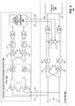
- FIG. 3 is a simplified circuit diagram of a transceiver 300 that estimates and corrects TX LO leakage according to an embodiment of the present invention.
- the transceiver 300 may include a transmitter 360 and loopback circuitry 310.
- the transmitter 360 may modulate a baseband signal shown as TX digital data 350, to convert it to an RF signal at a desired frequency.
- the loopback circuitry 310 enables the estimation of TX LO leakage by opening and shorting the loopback path via segments 361, 362; or changing the gain of the loopback path; or flipping the polarity of the loopback TX signal, or filtering out any LO harmonics.
- the loopback circuitry 310 may be implemented off-chip, or may reuse circuitry of an on-chip receiver.
- the transmitter 360 may include summers 326, 327; digital-to-analog converters (DACs) 333, 334; baseband filters 328, 329; and upconverters 337, 338.
- Summers 326, 327 may combine a compensation signal computed by a TX LO leakage estimation and correction unit 340 with a baseband signal transmitted via paths 365, 366 to cancel TX LO leakage.
- the DACs 333, 334 may convert a digital baseband signal to an analog signal. These units have the same functions and characteristics as those described above for FIG. 2 , unless described elsewhere herein.
- the exemplary loopback circuitry 310 may include a TX LO leakage estimation and correction unit 340; analog-to-digital converters (ADCs) 331,332; baseband filters 319, 321; downconverters 317, 318; coupling unit 320, which may include LO harmonic filters 315, 316 and buffers 311-314. These units have the same functions and characteristics as those described above for FIG. 2 , unless described elsewhere herein.
- ADCs analog-to-digital converters
- the loopback path (for example, segments 361, 362) is opened and closed, for example, by filters, buffers, and/or switches.
- the buffers 312 and 313 are not used. For example, they may be off or simply not included in the circuitry. Due to the formation of the loopback path for measurement, there may be disturbance to TX.
- the buffers 311 and 314 may be constantly enabled to reduce or substantially prevent any disturbance to TX via path 367.
- Two modes of operation may be performed sequentially to detect the level of TX LO leakage in the transceiver 300.
- the LO harmonic filters 315 and 316 are disabled such that the DC offset (DCa) of the loopback circuitry 310, including LO leakage of the downconverters 317 and 318, is measured.
- the LO harmonic filters 315 and 316 are enabled such that the TX signal is looped back to the loopback circuitry 310 via path segments 361 and 362 and a new DC offset (DCb) is measured.
- DCa and DCb should be the DC offset caused by the TX LO leakage.
- calibration error may result from impedance mismatch when transitioning between the two modes of operation, so DCb - DCa will also account for any DC offset caused by loopback LO leakage (also referred to as "RX LO leakage") variation.
- the last stage of the LO harmonic filters 315 and 316 may be constantly enabled to maintain a substantially constant impedance seen by the downconverters 317 and 318.
- the function of disabling and enabling the LO harmonic filters may be implemented in other ways.
- the gain of the LO harmonic filters may be changed between the first and second modes of operation, rather than completely disabling and enabling the LO harmonic filters 315 and 316.
- the polarity of the loopback transmit signal is flipped and measured. All four buffers 311-314 are used. Two modes of operation may be performed sequentially to detect the level of TX LO leakage in the transceiver 300. In a first mode of operation, buffers 311 and 314 are enabled and buffers 312 and 313 are disabled, and a DC offset (DC1) is measured. DC1 includes any DC offset caused by TX LO leakage, as well as any DC offset caused by the loopback circuitry 310. In a second mode of operation, buffers 312 and 313 are enabled and buffers 311 and 314 are disabled, and another DC offset (DC2) is measured. DC2 includes any DC offset caused by TX LO leakage of opposite polarity compared with DC1, as well as any DC offset caused by the loopback circuitry 210.
- DC1 includes any DC offset caused by TX LO leakage, as well as any DC offset caused by the loopback circuitry 210.
- the difference between DC and DC2, DC2 - DC 1 is approximately twice the level of the DC offset caused by TX LO leakage.
- the difference between DC1 and DC2 is caused by TX LO leakage alone, and an accurate measurement of TX LO leakage may be made. Additionally, this measurement effectively doubles the loopback path gain for the loopback TX signal, whereas the loopback TX noise is only 3 dB higher. Therefore, the signal-to-noise ratio of the loopback TX is 3dB higher.
- the difference between DC1 and DC2 may be minimized.
- Disturbance to TX may be minimized by slowing the transition between the two modes of operation relative to the TX signal when the four buffers 311-314 are placed at the front of loopback circuitry 310.
- the four buffers may also be placed inside filters 315, 316, or after filters 315, 316 (see Fig. 9), to minimize disturbance to TX without slowing the transition between the two modes of operation.
- Any number of buffers may be used, so long as the polarity of the loopback TX signal is flipped.
- all of the aforementioned buffers may be replaced with switches or other circuits, as long as the polarity of the loopback TX signal is flipped.
- switches When switches are used, the functional equivalent of an enabled buffer is a closed switch, and the functional equivalent of a disabled buffer is an open switch.
- the switches may be placed before the filters, inside the filters or after the filters.
- the LO harmonic filters 315, 316 may filter out harmonics of an LO signal.
- LO harmonics may arise.
- TX out lo t A 1 + B 1 cos ⁇ lo t + k 3 A 1 + B 3 cos 3 ⁇ lo t + k 5 A 1 + B 5 cos 5 ⁇ lo t +
- (A 1 + B 1 ) cos( ⁇ lo t) is the fundamental TX LO leakage to be detected and removed
- ⁇ lo is the angular frequency of the LO
- t is time
- a 1 is the amplitude of the fundamental TX LO leakage due to DC offset in the TX baseband
- B 1 is the amplitude of the fundamental TX LO leakage due to direct coupling of the LO to the TX output.
- the remaining terms represent higher order LO leakage frequency terms, where k 3 A 1 and k 5 A 1 result when a non-linear mixer is used for upconversion, and B 3 and B 5 are direct coupling terms when TX LO does not use a sine wave.
- RX out DC only ⁇ 1 A 1 + B 1 + ⁇ 3 k 3 A 1 + B 3 + ⁇ 5 k 5 A 1 + B 5 + where ⁇ 3 is the gain at the third harmonic, and ⁇ 5 is the gain at the fifth harmonic.
- the harmonic terms ⁇ 3 (k 3 A 1 +B 3 ) and ⁇ 5 (k 5 A 1 +B 5 ) reduce the accuracy of the TX LO leakage estimation, and should be removed.
- the LO harmonic filters 315, 316 may substantially attenuate the higher order terms ⁇ 3 (k 3 A 1 +B 3 ) and ⁇ 5 (k 5 A 1 +B 5 ), giving a signal closer to ⁇ 1 (A 1 +B 1 ), corresponding to the TX LO leakage for subsequent measurement by the loopback circuitry 310.
- Phase difference between the looped-back signal and the receiver's LO also corrupts TX LO estimation and may be accounted for in the estimation of TX LO leakage as described herein.
- the TX LO leakage may be cancelled by injecting a compensation signal corresponding to the level of estimated TX LO leakage via paths 363, 364.
- a digital compensation signal having in-phase and quadrature components L IC and L QC may be calculated by TX LO estimation and correction unit 340, and injected into the TX baseband via summers 326, 327.
- FIG. 4 shows another method for injecting the compensation signal into the TX baseband.
- FIG. 4 is a simplified circuit diagram of a transceiver 400 with TX LO leakage estimation and calibration applying DC offsets with DACs according to an embodiment of the present invention.
- the transceiver 400 may have the same components with the same functions and characteristics as those described above for FIGs. 2 and 3 , unless described elsewhere herein.
- the transceiver 400 may have DC offset DACs 471, 472 for applying DC offsets at TX baseband.
- the transceiver 400 compensates TX LO leakage by modifying the TX baseband signal after the signal has been converted to analog form by DACs 433,434.
- DC offset DACs 471, 472 convert the digital compensation signals L IC , L QC , which may be computed by TX LO leakage estimation and correction unit 440, to analog form and combines the compensation signal with the analog form of the TX signal prior to modulation by upconverters 437,438.
- LO harmonic filters anywhere prior to down conversion (such as prior to the buffers 411-414), using a harmonic rejection mixer in the loopback circuitry, or using a linear mixer such as a linear multiplier with a sine wave LO in the loopback receiver.
- Buffers may be embedded into the LO harmonic filters. Buffers may also be implemented with any isolating circuitry, such as CMOS source followers.
- the filters described above may be implemented with amplifiers.
- the LO harmonic filters may have multiple stages. It is also possible to effectively flip the polarity of the TX signal by switching the polarity of the LO signals of the loopback mixers. In such a method, the buffers 412 and 413 (shown in phantom) are not used.
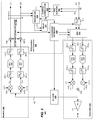
- FIG. 5 is a block diagram of an RF transceiver system 500 for estimating and correcting TX LO leakage according to an embodiment of the present invention.
- the system 500 may include a transmitter 510, a receiver 550, a TX LO leakage estimation and correction unit 530, and coupling unit 520, which may be provided in a common integrated circuit. These units have the same functions and characteristics as those described for FIGs. 2 to 4 , unless described elsewhere herein.
- the TX and RX signals are shown in their constituent I and Q components.
- the exemplary transmitter 510 may include digital filters 512.1, 512.2 and DACs 513, 514; upconverters 516.1, 516.2; a summer 519; and an amplifier 517. If the TX sampling rate is not matched to the DAC's (represented at 513, 514) sampling rate, the transmitter 510 may further include low pass filters 515.1, 515.2.
- the digital filters 512.1, 512.2 may enhance or reduce aspects of a signal for subsequent processing.
- the upconverters 516.1, 516.2 may convert signals to a designated carrier frequency with the aid of local oscillators having leakage components L IT and L QT .
- the low pass filters 515.1, 515.2 may be image rejection filters that attenuate images of transmit signals at multiples of the sampling frequency.
- the low-pass filters 515.1, 515.2 may match the data rate to the DAC sampling rate, and may allow the DACs 513, 514 to operate at a higher sampling rate to ease the image rejection requirements.
- the TX signal is sampled at the output of the power amplifier 517. In another embodiment, the TX signal is sampled at the output of the summer 519.
- a digital signal having components I(t) and Q(t) may be filtered by the digital filters 512.1,512.2 before being converted to an analog signal by the DACs 513, 514.
- the low pass filters 515.2,515.2 may further condition the analog signal before modulation by the upconverters 515.1, 516.2.
- the summer 519 may then combine the I(t) and Q(t) components and output a single signal.
- the signal may then be amplified by the power amplifier 517 and transmitted as an RF signal.
- the TX signal may be processed by a TX IQ and LO leakage compensation network (QEC) 518 prior to filtering and modulation as shown.
- QEC TX IQ and LO leakage compensation network
- the exemplary receiver 550 may include downconverters 555.1,555.2; anti-aliasing filters 551.1, 551.2; ADCs 552, 553; and digital filters 554.1, 554.2. These units have the same functions and characteristics as those described above for FIGs. 2 to 4 , unless described elsewhere herein.
- the downconverters 555.1, 555.2 may convert signals from a carrier frequency with the aid of local oscillators LO I and LO Q.
- the anti-aliasing filters 551.1, 551.2 may ensure an adequate sampling rate by subsequent ADCs to prevent aliasing.
- an RF signal may be demodulated by the downconverters 555.1, 555.2 to extract the original baseband signal having components I and Q.
- the analog signal may be filtered by the anti-aliasing filters 551.1, 551.2 before conversion to a digital signal by the ADCs 552, 553.
- the digital signal may be further processed by the digital filters 554.1, 554.2.
- the received signal (also referred to as "observed signal") may have leakage components L IR and L QR .
- a segment 521 of a loopback path may be formed by connecting the output of the transmitter via the filters 520, for example prior to amplification by amplifier 517 to the input of the receiver 550.
- a TX LO leakage correction signal may be injected into the transmit path via segment 522 after TX LO leakage has been measured. Additional circuitry described below may sample the signals using the loopback path to detect and compensate TX LO leakage.
- the resampler 534 may sample the output of the receiver 550 at nodes N5 and N6 at a resampling phase determined by the delay computer 531.
- the DC offset estimator 537 controlled by a LO leakage estimation process estimates the DC signal on the received signals.
- the LO leakage estimation process assures the estimation duration is sufficient to get a good estimate of the DC signals.
- the estimator 537 may be in the path (as shown), or sample the receive signal at nodes N3 and N4, without using summers 556.1 and 556.2 to apply any correction.
- the resampler 534 may output the sampled RX signal to the channel correlator 533.
- the channel correlator 533 correlates the samples provided by the FIFO buffer 532, sampled from the transmit path at nodes N1 and N2, against itself and by the samples provided by the resampler 534. That is, the channel correlator 533 is used to determine the following quantities: E s i n s i n s i n s q n s i n s q n s q n s q n r n q n r n
- the values are used to estimate the transmit-to-receive channel, h, based on well-known techniques.
- the channel, h may be used either to ascertain the phase difference between a received carrier phase and a receiver-generated LO at time " n ", ⁇ ( n ), (also referred to as "phase difference between TX and RX"), and/or track the phase difference variations over time. If the channel, h, is used to track the phase variation over time, then an accurate estimate of the phase difference between the TX and RX, ⁇ , may be ascertained initially, by injecting a strong in-phase dc signal into the in-phase component of the transmitter, and measuring the resultant received in-phase and quadrature dc signals.
- an iterative procedure (such as the one provided in method 700 below) may be used to update leakage compensation values L IC and L QC in accordance to the de-rotator equation given below. This procedure may be repeated, utilizing the values of L IC and L QC in the previous iteration, to refine the initial estimate of ⁇ .
- Other initialization techniques are also possible to measure ⁇ . For example, a complex DC signal may be injected and the received complex DC signal de-rotated such that the transmitted and received DC signals have the same phase.
- h rel h i l ⁇ h i g ⁇
- Transmit signaling may be used to ascertain the channel, h.
- Transmit signals may include a single or a combination of narrow- and wideband signals.
- the location of transmit signals relative to LO can be anywhere within the frequency span of the transmitter.
- transmit signaling can change over time. That is, additional channels may be added or removed, or the transmission frequency of a channel may change over time.
- the observed signal and the measured channel may contain a signaling dependent component.
- the measure channel may also include a signaling-dependent component that may change over time.
- the received signal may then be phase equalized relative to that of the transmit signal.
- the transmit signaling and its characteristics does not impact the phase difference between the TX and RX.
- phase difference between the TX and RX, ⁇ gives rise to coupling between the I and Q components of the TX LO signal.
- the QEC 518 network may substantially eliminate or minimize TX LO leakage by injecting a compensation signal with components L IC and L QC of equal magnitude and opposite polarity of the TX LO leakage components L IT and L QT into the transmitter 510.
- the value of ⁇ may be accurately ascertained by initially estimating TX LO leakage L IT and L QT .
- a strong in-phase dc signal injected into the in-phase component of the transmitter, and measuring the resultant received in-phase and quadrature dc signals, which are then compensated by initial measured L IT and L QT .
- an iterative procedure (such as the one provided in method 700 below) may be used to update leakage compensation values L IC and L QC in accordance to the de-rotator equation given above, by combining the current measured residual LO leakage with previous values, before applying a compensation signal to the transmit network.
- the DC offset estimator 537 may sample the received signal or estimate the DC offset of the received digitized signal by averaging observed samples. In an embodiment, the DC offset estimator 537 may sample the received signal without applying any correction, that is, without using summers 556.1 and 556.2 to apply any correction, and instead only samples the receive signal at nodes N3 and N4. In another embodiment, the DC offset estimator 537 estimates the DC offset by using a running average of samples. For example, a sample N may be obtained and stored by the DC offset estimator 537. A subsequent sample, N+1 may be obtained at nodes N3 and N4, and averaged with the previous N-1 samples by summers 556.1, 556.2 to compute a running average of samples. In an embodiment, the DC offset estimator 537 may use this or other well-known methods to estimate the DC offset of the received signal and output this estimate to LO leakage estimator 535.
- the LO leakage estimator 535 may estimate the level of LO leakage and apply correction factors L IC for the I component and L QC for the Q component of the TX signal via the QEC 518.
- the LO leakage estimator 535 may estimate TX LO leakage components L IT and L QT with the aid of the DC offset estimator 537, the delay computer 531, and the channel correlator 533 to compute the TX LO leakage.
- the LO leakage estimator 535 may control the filters 520 and the filters 511.
- the LO leakage estimator 535 may use an algorithm such as method 700 described herein.
- the QEC 518 may modify a signal having I(t) and Q(t) components with a compensation signal having components L IC and L QC .
- I(t) and Q(t) may be pre-processed by filters prior to processing in the QEC 518, and the output of the QEC 518 may be connected to any stage before filtering by digital filtering in a transmitter.
- L IC and L QC may be computed by a LO leakage estimator (such as the estimator 535 of FIG. 5 ).
- FIG. 6 illustrates an initialization calibration method 600 for estimating and compensating TX LO leakage.
- the method 600 may be a software algorithm stored in a control unit (such as the TX Estimation and Correction block 630 of FIG. 5 ) and may be executed by hardware and software components of a transceiver (such as the system 200 of FIG. 2 ).
- the method 600 estimates TX LO leakage by initially measuring the loop gain of the closed loop system and the phase difference between TX and RX. The values of the loop gain and phase difference are iteratively used to estimate L IT and L QT , and compensate them.
- the method 600 may initialize variables and counters such as the number of passes to perform, the number of LO leakage measurements to make, and phase measurement variables such as ⁇ and loopback gain (box 610).
- the method 600 may access and modify a system memory (not shown), which may store, track, and update the variables and counters.
- the method 700 resets switches (such as in the manner described above using switches or buffers) and initiates an RX DC offset measurement.
- the method 600 waits to allow processing time by the hardware specific blocks (such as the DC offset estimator 537 and LO leakage estimator 535 of FIG. 5 ) to settle to final values.
- step 640 the method flips switches and/or phase (such as in the manner described above using switches or buffers), and initiates the RX DC offset measurement in step 641 and waits for corresponding hardware (such as the DC offset estimator 537 of FIG. 5 ) to settle to its final value in step 642. If it is determined that the RX DC offset measurement is complete in step 643, the method 600 may compute and apply LO leakage compensation factors L IC and L QC in step 644 (for example via the QEC 518 of FIG. 5 ). In step 660, the method 600 queries whether there are any incomplete LO leakage measurements based on the variables and counters.
- step 620 the method returns to step 620 to measure RX DC offset.
- the method 600 may be repeated until all LO leakage measurements are complete. If all LO leakage measurements are determined to be complete in step 660, the method proceeds to step 670. In step 670, the method queries whether there are any incomplete passes based on the variables and counters. If there are incomplete passes, the method returns to step 610. The method 600 may be repeated until all desired passes are complete. It is also possible to use method 600 to track calibration based on a user's desire to make multiple passes. If all passes are complete in step 670, initialization is complete and the process 600 ends.
- the initialization method 600 may be performed in a single pass or multiple passes.
- a first pass of method 600 the estimation of ⁇ occurs without compensation values L IC and L QC , and there may be some coupling of TX LO leakage DC in the loopback path measurements. TX LO leakage may be compensated such that when the loopback path is opened, the observed DC measurements on the receiver is decoupled from that of the TX LO leakage.
- the estimation of ⁇ is made with compensation values L IC and L QC . If the initialization method 600 is performed in a single pass, only the first pass may be performed. If the initialization method 600 is performed in multiple passes, the algorithm reiterates as described above,
- step 650 the method initiates ⁇ and loop gain measurement in step 651 and waits for corresponding hardware to settle to its final value in step 652.
- step 653 if it is determined that the phase measurement is complete, the method may compute ⁇ and loop gain based on the measurements in step 680. Loop gain measurement may be used to match the RX LO leakage to the TX LO leakage.
- a data path may be enabled, and a channel may be estimated. The channel estimate may be used as reference to ascertain channel changes over time during a tracking calibration method, such as the method 700 described herein.
- step 680 the method 600 queries whether there are any remaining LO leakage measurements in step 660.
- the initialization calibration method 600 may be performed with the tracking calibration method 700.
- FIG. 7 illustrates a tracking method for estimating and correcting TX LO leakage, and a tracking calibration for a transceiver according to an embodiment of the present invention.
- the steps of the method 700 are the same as the corresponding steps described for FIG. 6 , unless described elsewhere herein.
- ⁇ may be measured from channel estimation.
- the method 700 may initialize variables and counters such as the number of LO leakage measurements to make, and phase measurement variables such as ⁇ and loopback gain (box 710).
- the method 700 may access and modify a system memory (not shown), which may store, track, and update the variables and counters. If it is determined in step 720 that channel measurement is desired, the method 800 initiates a channel measurement estimation in step 721 and waits for corresponding hardware (such as the channel correlator 533 of FIG. 5 ) to settle to its final value in step 722. If it is determined that the channel measurement is complete in step 723, the method 700 may update ⁇ according to the equation given above for modifying the de-rotator component at time n.
- the tracking method 700 may be used throughout operation of the circuit to track changes in the channel conditions to measure and compensate the residual LO leakage in the system over time and in accordance to the de-rotator equation given above.
- step 720 If it is determined in step 720 that channel measurement is not desired, the method 700 initiates coarse carrier power estimation in step 730. After initiating coarse power measurement in step 730, the method 700 waits for corresponding hardware to settle to its final value in step 731. In step 732, the method 700 queries whether coarse power measurement is complete. If it is not complete, it continues to wait. Otherwise, it continues to step 733, in which estimation parameters are set. In step 740, the method 700 resets the switches or phase and initiates an RX DC offset measurement. The method 700 waits for corresponding hardware to settle to its final value in step 731. Once DC measurement is complete in step 742, the method flips the switches or phase and initiates another RX DC offset measurement in step 743. The method 700 waits for corresponding hardware to settle to its final value in step 744.
- step 745 the method 700 queries whether the RX DC offset measurement is complete. If it is, the method 700 proceeds to step 746 in which it computes and applies LO leakage compensation factors. The method 700 then checks whether there are remaining LO leakage measurements to be completed in step 760. If there are incomplete LO leakage measurements, the method 700 proceeds to step 740 in which the switches or phase are reset and another RX DC offset measurement is taken. The method 700 then proceeds through the steps as described above. However, if all LO leakage measurements are complete, then the method 700 proceeds to step 720 in which it queries whether the channel is to be measured and proceeds through subsequent steps as described above.
- Tracking calibration method 700 may be performed alone to estimate and cancel TX LO leakage, or may be performed following an initialization calibration method such as the method 600.
- the two methods may be implemented as two modes of operation in a control unit, or may be implemented separately on discrete circuitry.
- Fig. 3 is shown as a differential circuit, the circuit 300 may be implemented in a single-ended fashion with the filtering, connect/disconnect, and gain changing functionalities described herein. Modifications, variations, and improvements are possible in light of the teachings above and the claims below, and are intended to be within the scope of the invention.
Landscapes
- Engineering & Computer Science (AREA)
- Computer Networks & Wireless Communication (AREA)
- Signal Processing (AREA)
- Physics & Mathematics (AREA)
- Electromagnetism (AREA)
- Transceivers (AREA)
- Position Fixing By Use Of Radio Waves (AREA)
Claims (14)
- Schaltung zum Detektieren und Korrigieren eines Lecks eines Sender-Hilfsoszillators, LO, in einem System, das einen Sender (210) und einen Empfänger (250) besitzt, wobei der Sender einen Aufwärtsumsetzer besitzt und der Empfänger einen Abwärtsumsetzer besitzt, wobei die Schaltung Folgendes umfasst:eine Kopplungseinheit (220), die an einen Ausgang des Senders und an einen Eingang des Empfängers gekoppelt ist, wobei die Kopplungseinheit dazu ausgelegt ist, in einer ersten Betriebsart zu arbeiten, um ein Schleifenschaltungs-Sendesignal bereitzustellen, und in einer zweiten Betriebsart zu arbeiten, wobei die Polarität des Schleifenschaltungs-Sendesignals invertiert ist;eine Schätzungs-und-Korrigiereinheit (230), die an einen Eingang des Senders und an einen Ausgang des Empfängers gekoppelt ist, wobei die Schaltung zu Folgendem ausgelegt ist:Messen eines ersten Gleichstrom-Versatzes eines Signals von der Kopplungseinheit in der ersten Betriebsart;Messen eines zweiten Gleichstrom-Versatzes des Signals in der zweiten Betriebsart; undBestimmen des Lecks des Sender-LO aus einem Unterschied zwischen dem ersten Gleichstrom-Versatz und dem zweiten Gleichstrom-Versatz.
- Schaltung nach Anspruch 1, wobei die Kopplungseinheit (220) den Sender und den Empfänger elektrisch miteinander verbinden und voneinander trennen kann, um das Leck des Sender-LO zu korrigieren.
- Schaltung nach Anspruch 1 oder 2, wobei eine Verstärkung der Kopplungseinheit (220) auswählbar und veränderbar ist.
- Schaltung nach Anspruch 1, 2 oder 3, wobei die Kopplungseinheit Folgendes enthält:einen ersten Puffer und/oder einen ersten Schalter, die an den Ausgang des Senders und den Eingang des Empfängers gekoppelt sind; undeinen zweiten Puffer und/oder einen zweiten Schalter, die an den Ausgang des Senders und den Eingang des Empfängers gekoppelt sind.
- Schaltung nach Anspruch 1, 2 oder 3, wobei die Kopplungseinheit Folgendes enthält:ein erstes Filter, das einen Eingang, der an einen ersten differentiellen Ausgang des Senders gekoppelt ist, und einen Ausgang, der an einen ersten differentiellen Eingang des Empfängers gekoppelt ist, besitzt;ein zweites Filter, das einen Eingang, der an einen ersten differentiellen Ausgang des Senders gekoppelt ist, und einen Ausgang, der an einen zweiten differentiellen Eingang des Empfängers gekoppelt ist, besitzt;ein drittes Filter, das einen Eingang, der an einen zweiten differentiellen Ausgang des Senders gekoppelt ist, und einen Ausgang, der an den ersten differentiellen Eingang des Empfängers gekoppelt ist, besitzt; undein viertes Filter, das einen Eingang, der an den zweiten differentiellen Ausgang des Senders gekoppelt ist, und einen Ausgang, der an den zweiten differentiellen Eingang des Empfängers gekoppelt ist, besitzt;wobei das erste Filter, das zweite Filter, das dritte Filter und das vierte Filter jeweils Folgendes enthalten: einen Puffer und/oder einen Schalter.
- Schaltung nach Anspruch 5, wobei eines der Folgenden zutrifft:a) die Schaltung umfasst ferner ein erstes LO-Oberwellenfilter, das einen Eingang, der an den Ausgang des ersten Filters und den Ausgang des dritten Filters gekoppelt ist, und einen Ausgang, der an den ersten differentiellen Eingang des Empfängers gekoppelt ist, besitzt; und ein zweites LO-Oberwellenfilter, das einen Eingang, der an den Ausgang des zweiten Filters und den Ausgang des vierten Filters gekoppelt ist, und einen Ausgang, der an den zweiten differentiellen Eingang des Empfängers gekoppelt ist, besitzt;b) die Schaltung umfasst ferner ein erstes LO-Oberwellenfilter, das einen Eingang, der an den ersten differentiellen Ausgang des Senders gekoppelt ist, und einen Ausgang, der an den Eingang des ersten Filters und den Eingang des zweiten Filters gekoppelt ist, besitzt; und ein zweites LO-Oberwellenfilter, das einen Eingang, der an den zweiten differentiellen Ausgang des Senders gekoppelt ist, und einen Ausgang, der an den Eingang des dritten Filters und den Eingang des vierten Filters gekoppelt ist, besitzt.
- Schaltung nach einem der vorhergehenden Ansprüche, wobei der Sender ein Signal sendet und die Ausgabe der Schätzungs-und-Korrigiereinheit vor der Signalausgabe des Senders mit dem Signal des Senders kombiniert ist.
- Schaltung nach Anspruch 7, wobei die Ausgabe der Schätzungs-und-Korrigiereinheit vor der Kombination mit dem Signal des Senders in eine analoge Form umgesetzt wird.
- Schaltung nach einem der vorhergehenden Ansprüche, wobei die Schätzungs-und-Korrigiereinheit Folgendes enthält:einen Gleichstrom-Versatz-Schätzer, der an einen ersten differentiellen Ausgang und einen zweiten differentiellen Ausgang des Empfängers gekoppelt ist;einen Resampler, der an den ersten differentiellen Ausgang und den zweiten differentiellen Ausgang des Empfängers nach dem Gleichstrom-Versatz-Schätzer gekoppelt ist;einen Verzögerungscomputer, der an den Resampler gekoppelt ist;einen Kanal-Korrelator, der an den Resampler gekoppelt ist;mindestens einen First-In-First-Out-Puffer, der einen Eingang, der an einen ersten differentiellen Eingang und einen zweiten differentiellen Eingang des Senders gekoppelt ist, und einen Ausgang, der an den Kanal-Korrelator gekoppelt ist, besitzt;ein LO-Leck-Kompensationsnetz, das nach dem mindestens einen First-In-First-Out-Puffer an den Eingang des Senders gekoppelt ist; undeinen LO-Leck-Schätzer, der an den Gleichstrom-Versatz-Schätzer, den Verzögerungscomputer, den Kanal-Korrelator, das Hilfsoszillatorleck-Leck-Kompensationsnetz und die Kopplungseinheit gekoppelt ist.
- Verfahren zum Messen eines Lecks eines Sender-Hilfsoszillators, LO, unter Verwendung einer Schaltungsanordnung auf einem Schleifenschaltungspfad, wobei die Schaltungsanordnung an einen ersten differentiellen Ausgang und einen zweiten differentiellen Ausgang des Senders und an einen ersten differentiellen Eingang und einen zweiten differentiellen Eingang eines Empfängers gekoppelt ist, wobei das Verfahren Folgendes umfasst:Messen eines ersten Gleichstrom-Versatzes der Schleifenschaltungs-Schaltungsanordnung;Invertieren einer Polarität eines Sendesignals unter Verwendung der Schaltungsanordnung auf dem Schleifenschaltungspfad;Messen eines zweiten Gleichstrom-Versatzes der Schleifenschaltungs-Schaltungsanordnung; undBestimmen des Lecks des Sender-Hilfsoszillators aus einem Unterschied zwischen dem ersten Gleichstrom-Versatz und dem zweiten Gleichstrom-Versatz.
- Verfahren nach Anspruch 10, wobei:der erste Gleichstrom-Versatz gemessen wird, indem ein erstes Filter, das an den ersten differentiellen Ausgang des Senders und den ersten differentiellen Eingang zu dem Empfänger gekoppelt ist, aktiviert wird und ein zweites Filter, das an den zweiten differentiellen Ausgang des Senders und den zweiten differentiellen Eingang zu dem Empfänger gekoppelt ist, aktiviert wird;die Polarität des Sendesignals umgekehrt wird und der zweite Gleichstrom-Versatz gemessen wird, indem das erste Filter und das zweite Filter deaktiviert werden und ein drittes Filter, das an den ersten differentiellen Ausgang des Senders und den zweiten differentiellen Eingang zu dem Empfänger gekoppelt ist, aktiviert wird und ein viertes Filter, das an den zweiten differentiellen Ausgang des Senders und den ersten differentiellen Eingang zu dem Empfänger gekoppelt ist, aktiviert wird; unddas erste Filter, das zweite Filter, das dritte Filter und das vierte Filter jeweils Folgendes enthalten: einen Puffer und/oder einen Schalter.
- Verfahren nach Anspruch 10, das ferner das Einspeisen eines Kompensationssignals in einen Pfad des Senders umfasst, wobei das Kompensationssignal dem bestimmten Leck des Sender-LO entspricht.
- Verfahren zum Initialisieren und Kalibrieren einer Messung eines Lecks eines Sender-Hilfsoszillators, LO, das Folgendes umfasst:Initialisieren mindestens einer Variable;Zurücksetzen von Folgendem: einem Schalter und/oder einer Phase und Beginnen einer ersten Empfangs-Gleichstrommessung;Warten auf das Festsetzen von Hardware-Komponenten auf Endwerte;in Reaktion auf eine Bestimmung, dass eine Phasenmessung gewünscht ist:Initialisieren einer Sende-und-Empfangs-Phasendifferenzmessung und einer Schleifenverstärkungsmessung;Warten auf das Festsetzen von Hardware-Komponenten auf Endwerte;Berechnen einer Sende-und-Empfangs-Diskrepanz und einer Schleifenverstärkung anhand der Sende-und-Empfangs-Diskrepanzmessung und der Schleifenverstärkungsmessung in Reaktion auf eine Bestimmung, dass die Phasenmessung abgeschlossen ist;in Reaktion auf eine Bestimmung, dass eine Messung des Lecks des Sender-LO gewünscht ist, Folgendes:Invertieren der Phase;Beginnen einer zweiten Empfangs-Gleichstrommessung;Warten auf das Festsetzen von Hardware-Komponenten auf Endwerte; undBerechnen und Anwenden von Kompensationsfaktoren für das Leck des Sender-LO in Reaktion auf eine Bestimmung, dass die zweite Gleichstrommessung abgeschlossen ist;Zurückkehren zum Zurücksetzen von Folgendem in Reaktion auf eine Bestimmung, dass Messungen des Lecks des Sender-LO unvollständig sind: einem Schalter und/oder einer Phase und Beginnen einer ersten Empfangs-Gleichstrommessung; undZurückkehren zum Initialisieren von Variablen in Reaktion auf eine Bestimmung, dass mindestens ein Durchgang unvollständig ist.
- Verfahren zum Verfolgen der Kalibrierung einer Messung eines Lecks eines Sender-Hilfsoszillators, LO, indem eine Sende-und-Empfangs-Phasenmessung aktualisiert wird, wobei das Verfahren Folgendes umfasst:Initialisieren von Variablen;in Reaktion auf eine Bestimmung, dass eine Kanalmessung gewünscht ist:Beginnen einer Schätzung einer Kanalmessung;Warten auf das Festsetzen von Hardware-Komponenten auf Endwerte; undBerechnen einer Sende-und-Empfangs-Phase und Aktualisieren der Sende-und-Empfangs-Phasenmessung in Reaktion auf eine Bestimmung, dass die Kanalmessung abgeschlossen ist;in Reaktion auf eine Bestimmung, dass eine Kanalmessung nicht gewünscht ist, Folgendes:Beginnen einer groben Leistungsmessung;Warten auf das Festsetzen von Hardware-Komponenten auf Endwerte;in Reaktion auf eine Bestimmung, dass die grobe Leistungsmessung abgeschlossen ist, Folgendes:Festlegen von Schätzparametern;Zurücksetzen von Folgendem: einem Schalter und/oder einer Phase und Beginnen einer ersten Empfangs-Gleichstrommessung;Warten auf das Festsetzen von Hardware-Komponenten auf Endwerte;in Reaktion auf eine Bestimmung, dass die erste Gleichstrommessung abgeschlossen ist, Folgendes:Invertieren der Phase;Beginnen einer zweiten Empfangs-Gleichstrommessung;Warten auf das Festsetzen von Hardware-Komponenten auf Endwerte; undBerechnen und Anwenden von Kompensationsfaktoren für das Leck des Sender-LO in Reaktion auf eine Bestimmung, dass die zweite Empfangs-Gleichstrommessung abgeschlossen ist;Zurückkehren zum Zurücksetzen von Folgendem in Reaktion auf eine Bestimmung, dass mindestens eine Messung des Lecks des Sender-LO übrig bleibt: eines Schalters und/oder einer Phase und Beginnen einer ersten Empfangs-Gleichstrommessung.
Applications Claiming Priority (1)
| Application Number | Priority Date | Filing Date | Title |
|---|---|---|---|
| US13/826,365 US9787415B2 (en) | 2013-03-14 | 2013-03-14 | Transmitter LO leakage calibration scheme using loopback circuitry |
Publications (3)
| Publication Number | Publication Date |
|---|---|
| EP2779472A2 EP2779472A2 (de) | 2014-09-17 |
| EP2779472A3 EP2779472A3 (de) | 2014-12-17 |
| EP2779472B1 true EP2779472B1 (de) | 2016-04-27 |
Family
ID=50442322
Family Applications (1)
| Application Number | Title | Priority Date | Filing Date |
|---|---|---|---|
| EP14157512.6A Active EP2779472B1 (de) | 2013-03-14 | 2014-03-03 | Sender-LO-Leckkalibrierungsschema unter Verwendung von Prüfschleifenschaltungsanordnung |
Country Status (3)
| Country | Link |
|---|---|
| US (1) | US9787415B2 (de) |
| EP (1) | EP2779472B1 (de) |
| CN (1) | CN104052507B (de) |
Cited By (2)
| Publication number | Priority date | Publication date | Assignee | Title |
|---|---|---|---|---|
| EP4243282A1 (de) * | 2022-03-09 | 2023-09-13 | Apple Inc. | Verstärker mit geteiltem eingang zum schutz vor gleichstromoffset |
| US12512873B2 (en) * | 2023-10-11 | 2025-12-30 | Hong Kong Applied Science And Technology Research Institute Co., Ltd | Method of estimating local oscillator leakage |
Families Citing this family (31)
| Publication number | Priority date | Publication date | Assignee | Title |
|---|---|---|---|---|
| US9252831B2 (en) * | 2013-03-01 | 2016-02-02 | Qualcomm Incorporated | Multi-tap adaptive filter for transmit signal leakage cancellation |
| TWI542220B (zh) * | 2013-12-25 | 2016-07-11 | Digital TV signal receiving method and system thereof | |
| US10128879B2 (en) * | 2014-03-31 | 2018-11-13 | Intel IP Corporation | Enhanced receive sensitivity for concurrent communications |
| KR102282475B1 (ko) * | 2014-09-30 | 2021-07-27 | 바야르 이미징 리미티드 | 멀티-모듈 시스템에서의 기준 신호 분배 |
| US9673914B2 (en) | 2015-08-11 | 2017-06-06 | Keysight Technologies, Inc. | Method and apparatus for spectral stitching using reference channel and a pilot tone |
| WO2017034959A1 (en) | 2015-08-21 | 2017-03-02 | Viasat, Inc. | Method and system in which a remote module assists in counteracting i/q imbalance and/or dc offset errors |
| US9810726B2 (en) * | 2015-09-09 | 2017-11-07 | Keysight Technologies, Inc. | Method and system for calibrating phases of comb teeth in comb signal with pilot tone and using calibrated comb teeth phases to measure a device under test |
| US9698919B1 (en) | 2015-12-28 | 2017-07-04 | Keysight Technologies, Inc. | Method and apparatus for spectral stitching discontinuous spectra using reference channel, pilot tones and comb signal |
| DE102016110344A1 (de) * | 2016-06-03 | 2017-12-07 | Infineon Technologies Ag | Rf-empfänger mit eingebauter selbsttestfunktion |
| EP3300267B1 (de) * | 2016-09-21 | 2021-02-24 | Intel IP Corporation | Verfahren zur erhöhung einer genauigkeit einer rückkopplungskalibrierung eines sendeempfängers und sendeempfängerschaltung |
| US11012104B2 (en) | 2017-03-03 | 2021-05-18 | Analog Devices, Inc. | Apparatus and methods for calibrating radio frequency transmitters to compensate for common mode local oscillator leakage |
| JP2018164183A (ja) * | 2017-03-24 | 2018-10-18 | 富士通株式会社 | 通信装置および歪補償方法 |
| US10135472B1 (en) | 2017-08-29 | 2018-11-20 | Analog Devices Global | Apparatus and methods for compensating radio frequency transmitters for local oscillator leakage |
| TWI666897B (zh) * | 2017-09-04 | 2019-07-21 | 瑞昱半導體股份有限公司 | 處理訊號干擾的裝置及方法 |
| US10805130B2 (en) | 2017-09-12 | 2020-10-13 | Intel IP Corporation | Signal cancellation system and method |
| KR102471074B1 (ko) * | 2018-01-30 | 2022-11-25 | 삼성전자주식회사 | Rf 신호 전송 장치 및 그의 제어 방법 |
| WO2019152793A1 (en) * | 2018-02-02 | 2019-08-08 | Viasat, Inc. | Radio frequency loopback for transceivers |
| WO2019164052A1 (en) * | 2018-02-22 | 2019-08-29 | Lg Electronics Inc. | Method of controlling harmonics and mobile terminal performing thereof |
| US10476538B2 (en) | 2018-02-22 | 2019-11-12 | Lg Electronics Inc. | Method of controlling harmonics and mobile terminal performing thereof |
| CN115989647B (zh) | 2020-07-22 | 2025-11-11 | 美国亚德诺半导体公司 | Rf前端lo泄漏和正交误差参数的确定 |
| CN120691900A (zh) * | 2020-08-07 | 2025-09-23 | 亚德诺半导体国际无限责任公司 | 无线电收发器的设备和方法 |
| CN116114224B (zh) * | 2020-08-13 | 2025-09-05 | 华为技术有限公司 | 发射机系统及电子设备 |
| TWI739663B (zh) | 2020-11-16 | 2021-09-11 | 瑞昱半導體股份有限公司 | 校正傳送器的方法 |
| CN115514433A (zh) * | 2021-06-22 | 2022-12-23 | 中兴通讯股份有限公司 | 本振泄漏信号的检测方法、抑制方法、终端及存储介质 |
| US12206441B2 (en) * | 2022-03-31 | 2025-01-21 | Dell Products L.P. | Detection and cancellation of unwanted signals in a wireless communication radio unit |
| US12224782B2 (en) | 2022-04-14 | 2025-02-11 | Dell Products L.P. | Detection, cancellation, and evaluation of signals in a wireless communication radio unit |
| US12191898B2 (en) * | 2022-05-23 | 2025-01-07 | Qualcomm Incorporated | Local oscillator leakage reporting |
| US12294398B2 (en) * | 2022-06-27 | 2025-05-06 | Texas Instruments Incorporated | Estimating and correcting transmitter local oscillator leakage in loopback path |
| US11683026B1 (en) | 2022-08-30 | 2023-06-20 | International Business Machines Corporation | Calibrating signal currents in a radio frequency signal generator |
| US12483278B2 (en) | 2022-11-15 | 2025-11-25 | International Business Machines Corporation | Spur and image suppression in a radio frequency signal generator |
| CN116684012A (zh) * | 2023-07-03 | 2023-09-01 | 易兆微电子(杭州)股份有限公司 | 一种系统中发射器lo泄漏的校准方法、装置、设备及介质 |
Family Cites Families (20)
| Publication number | Priority date | Publication date | Assignee | Title |
|---|---|---|---|---|
| US3449696A (en) * | 1965-04-12 | 1969-06-10 | Claude C Routh | Dual section all pass lattice filter wherein nonlinearities of two sections cancel |
| US4785270A (en) * | 1987-12-30 | 1988-11-15 | Motorola Inc. | Monolithic lattice saw filter |
| CA2069369C (en) * | 1992-05-25 | 1995-12-05 | Robert C. Peach | Filterbank using surface acoustic wave technology |
| GB9423027D0 (en) * | 1994-11-15 | 1995-01-04 | Univ Bristol | Full-duplex radio transmitter/receiver |
| US6960962B2 (en) | 2001-01-12 | 2005-11-01 | Qualcomm Inc. | Local oscillator leakage control in direct conversion processes |
| US7558351B2 (en) * | 2004-02-10 | 2009-07-07 | Wionics Research | Super harmonic filter and method of filtering frequency components from a signal |
| US7280805B2 (en) | 2004-07-09 | 2007-10-09 | Silicon Storage Technology, Inc. | LO leakage and sideband image calibration system and method |
| US8036622B2 (en) * | 2005-09-28 | 2011-10-11 | Qualcomm, Incorporated | DC offset cancellation circuit for a receiver |
| US8040982B1 (en) * | 2005-10-18 | 2011-10-18 | Marvell International Ltd. | Phase-adjusted channel estimation for frequency division multiplexed channels |
| FI20055632A0 (fi) | 2005-11-30 | 2005-11-30 | Nokia Corp | Paikallisoskillaattorin vuodon vaimentaminen radiolähettimessä |
| KR100746747B1 (ko) | 2006-02-06 | 2007-08-06 | 삼성전자주식회사 | Rfid 리더 |
| KR100710125B1 (ko) | 2006-02-23 | 2007-04-20 | 지씨티 세미컨덕터 인코포레이티드 | Iq 불일치 및 반송파 누설을 보상하는 송수신 회로 및 그제어 방법 |
| ATE515828T1 (de) | 2006-03-31 | 2011-07-15 | Nokia Siemens Networks Spa | Sender mit unterdrücktem träger,und verfahren dazu |
| KR100801871B1 (ko) | 2006-06-30 | 2008-02-11 | 지씨티 세미컨덕터 인코포레이티드 | 송신 반송파 누설 보상 방법 및 이를 이용하는 송수신 회로 |
| US7876867B2 (en) | 2006-08-08 | 2011-01-25 | Qualcomm Incorporated | Intermodulation distortion detection and mitigation |
| US7856048B1 (en) | 2006-11-20 | 2010-12-21 | Marvell International, Ltd. | On-chip IQ imbalance and LO leakage calibration for transceivers |
| US8135348B2 (en) | 2007-03-27 | 2012-03-13 | Qualcomm, Incorporated | Rejection of transmit signal leakage in wireless communication device |
| US8755756B1 (en) * | 2009-04-29 | 2014-06-17 | Qualcomm Incorporated | Active cancellation of interference in a wireless communication system |
| US8514918B2 (en) * | 2010-09-24 | 2013-08-20 | Intel Corporation | Close-loop power transmission calibration |
| US8659456B2 (en) * | 2011-11-16 | 2014-02-25 | Mediatek Inc. | Electronic device and transmitter DC offset calibration method thereof |
-
2013
- 2013-03-14 US US13/826,365 patent/US9787415B2/en active Active
-
2014
- 2014-03-03 EP EP14157512.6A patent/EP2779472B1/de active Active
- 2014-03-14 CN CN201410093865.7A patent/CN104052507B/zh active Active
Cited By (5)
| Publication number | Priority date | Publication date | Assignee | Title |
|---|---|---|---|---|
| EP4243282A1 (de) * | 2022-03-09 | 2023-09-13 | Apple Inc. | Verstärker mit geteiltem eingang zum schutz vor gleichstromoffset |
| US11894866B2 (en) | 2022-03-09 | 2024-02-06 | Apple Inc. | Split input amplifier for protection from DC offset |
| US12009847B2 (en) | 2022-03-09 | 2024-06-11 | Apple Inc. | Split input amplifier for protection from DC offset |
| US12244329B2 (en) | 2022-03-09 | 2025-03-04 | Apple Inc. | Split input amplifier for protection from DC offset |
| US12512873B2 (en) * | 2023-10-11 | 2025-12-30 | Hong Kong Applied Science And Technology Research Institute Co., Ltd | Method of estimating local oscillator leakage |
Also Published As
| Publication number | Publication date |
|---|---|
| US9787415B2 (en) | 2017-10-10 |
| CN104052507A (zh) | 2014-09-17 |
| EP2779472A2 (de) | 2014-09-17 |
| EP2779472A3 (de) | 2014-12-17 |
| CN104052507B (zh) | 2017-04-26 |
| US20140269863A1 (en) | 2014-09-18 |
Similar Documents
| Publication | Publication Date | Title |
|---|---|---|
| EP2779472B1 (de) | Sender-LO-Leckkalibrierungsschema unter Verwendung von Prüfschleifenschaltungsanordnung | |
| US9621337B2 (en) | Adaptive I/O mismatch calibration | |
| KR101234963B1 (ko) | Ofdm fdd 통신 시스템에서의 송신 및 수신 경로들의 i/q 교정 | |
| EP1214795B1 (de) | Vorrichtung zur störsignalkompensation in einem direktkonversionssender-empfänger und verfahren dazu | |
| US12047105B2 (en) | Apparatus and methods for DC-offset estimation | |
| CN105490973B (zh) | Iq信号校准方法及装置 | |
| US20040219884A1 (en) | Method and system for measuring receiver mixer IQ mismatch | |
| CN106817084A (zh) | 用于收发器中的局部振荡器的相位同步的装置和方法 | |
| US20150350000A1 (en) | Calibration method and calibration apparatus for calibrating mismatch between first signal path and second signal path of transmitter/receiver | |
| US11146276B2 (en) | Noise reduction and spur and distortion cancellation techniques | |
| US8027376B2 (en) | Method and system for measuring IQ path mismatch | |
| US8711904B2 (en) | Calibration method for non-ideal transceivers | |
| US20090004975A1 (en) | Electrical device comprising analog frequency conversion circuitry and method for delivering characteristics thereof | |
| US8526533B2 (en) | Systems and methods for measuring I-Q mismatch | |
| KR101980862B1 (ko) | 트랜시버 내 국부 발진기의 위상 동기화를 위한 장치 및 방법 | |
| EP3151500B1 (de) | Frequenzselektive quadraturbasisbandverbindungslöschung | |
| EP4513789A1 (de) | Verfahren und vorrichtung zur kalibrierung eines sende-empfängers | |
| EP1130866A1 (de) | Korrektur von Quadratur- soweiVerstärkungsfehlern in Homodynempfängern | |
| KR102921162B1 (ko) | 수신기 | |
| US20180083823A1 (en) | Transmission and reception circuit, transceiver, and method of correcting time difference of signal | |
| He et al. | An anti-image interference quadrature IF architecture for satellite receivers | |
| EP2779553A2 (de) | Geichstromvorspannungsschätzung eines Funkfrequenzmischers | |
| EP1496610B1 (de) | Frequenzumsetzer unter Verwendung von Unterdrückung der Trägerselbstmischung | |
| Van Rooyen et al. | Non-iterative compensation for software-defined radio quadrature front-end inaccuracies | |
| Craninckx et al. | Automatic calibration of a direct upconversion transmitter |
Legal Events
| Date | Code | Title | Description |
|---|---|---|---|
| PUAI | Public reference made under article 153(3) epc to a published international application that has entered the european phase |
Free format text: ORIGINAL CODE: 0009012 |
|
| 17P | Request for examination filed |
Effective date: 20140303 |
|
| AK | Designated contracting states |
Kind code of ref document: A2 Designated state(s): AL AT BE BG CH CY CZ DE DK EE ES FI FR GB GR HR HU IE IS IT LI LT LU LV MC MK MT NL NO PL PT RO RS SE SI SK SM TR |
|
| AX | Request for extension of the european patent |
Extension state: BA ME |
|
| PUAL | Search report despatched |
Free format text: ORIGINAL CODE: 0009013 |
|
| AK | Designated contracting states |
Kind code of ref document: A3 Designated state(s): AL AT BE BG CH CY CZ DE DK EE ES FI FR GB GR HR HU IE IS IT LI LT LU LV MC MK MT NL NO PL PT RO RS SE SI SK SM TR |
|
| AX | Request for extension of the european patent |
Extension state: BA ME |
|
| RIC1 | Information provided on ipc code assigned before grant |
Ipc: H04B 1/52 20060101AFI20141111BHEP |
|
| R17P | Request for examination filed (corrected) |
Effective date: 20150610 |
|
| RBV | Designated contracting states (corrected) |
Designated state(s): AL AT BE BG CH CY CZ DE DK EE ES FI FR GB GR HR HU IE IS IT LI LT LU LV MC MK MT NL NO PL PT RO RS SE SI SK SM TR |
|
| REG | Reference to a national code |
Ref country code: DE Ref legal event code: R079 Ref document number: 602014001618 Country of ref document: DE Free format text: PREVIOUS MAIN CLASS: H04B0001520000 Ipc: H04B0001525000 |
|
| GRAP | Despatch of communication of intention to grant a patent |
Free format text: ORIGINAL CODE: EPIDOSNIGR1 |
|
| RIC1 | Information provided on ipc code assigned before grant |
Ipc: H04B 15/04 20060101ALI20151014BHEP Ipc: H04B 1/525 20150101AFI20151014BHEP Ipc: H04B 17/11 20150101ALI20151014BHEP |
|
| INTG | Intention to grant announced |
Effective date: 20151103 |
|
| GRAS | Grant fee paid |
Free format text: ORIGINAL CODE: EPIDOSNIGR3 |
|
| GRAA | (expected) grant |
Free format text: ORIGINAL CODE: 0009210 |
|
| AK | Designated contracting states |
Kind code of ref document: B1 Designated state(s): AL AT BE BG CH CY CZ DE DK EE ES FI FR GB GR HR HU IE IS IT LI LT LU LV MC MK MT NL NO PL PT RO RS SE SI SK SM TR |
|
| REG | Reference to a national code |
Ref country code: GB Ref legal event code: FG4D |
|
| REG | Reference to a national code |
Ref country code: CH Ref legal event code: EP |
|
| REG | Reference to a national code |
Ref country code: AT Ref legal event code: REF Ref document number: 795785 Country of ref document: AT Kind code of ref document: T Effective date: 20160515 |
|
| REG | Reference to a national code |
Ref country code: IE Ref legal event code: FG4D |
|
| REG | Reference to a national code |
Ref country code: DE Ref legal event code: R096 Ref document number: 602014001618 Country of ref document: DE |
|
| REG | Reference to a national code |
Ref country code: LT Ref legal event code: MG4D |
|
| REG | Reference to a national code |
Ref country code: NL Ref legal event code: MP Effective date: 20160427 |
|
| REG | Reference to a national code |
Ref country code: AT Ref legal event code: MK05 Ref document number: 795785 Country of ref document: AT Kind code of ref document: T Effective date: 20160427 |
|
| PG25 | Lapsed in a contracting state [announced via postgrant information from national office to epo] |
Ref country code: NL Free format text: LAPSE BECAUSE OF FAILURE TO SUBMIT A TRANSLATION OF THE DESCRIPTION OR TO PAY THE FEE WITHIN THE PRESCRIBED TIME-LIMIT Effective date: 20160427 |
|
| PG25 | Lapsed in a contracting state [announced via postgrant information from national office to epo] |
Ref country code: NO Free format text: LAPSE BECAUSE OF FAILURE TO SUBMIT A TRANSLATION OF THE DESCRIPTION OR TO PAY THE FEE WITHIN THE PRESCRIBED TIME-LIMIT Effective date: 20160727 Ref country code: PL Free format text: LAPSE BECAUSE OF FAILURE TO SUBMIT A TRANSLATION OF THE DESCRIPTION OR TO PAY THE FEE WITHIN THE PRESCRIBED TIME-LIMIT Effective date: 20160427 Ref country code: LT Free format text: LAPSE BECAUSE OF FAILURE TO SUBMIT A TRANSLATION OF THE DESCRIPTION OR TO PAY THE FEE WITHIN THE PRESCRIBED TIME-LIMIT Effective date: 20160427 Ref country code: FI Free format text: LAPSE BECAUSE OF FAILURE TO SUBMIT A TRANSLATION OF THE DESCRIPTION OR TO PAY THE FEE WITHIN THE PRESCRIBED TIME-LIMIT Effective date: 20160427 |
|
| PG25 | Lapsed in a contracting state [announced via postgrant information from national office to epo] |
Ref country code: PT Free format text: LAPSE BECAUSE OF FAILURE TO SUBMIT A TRANSLATION OF THE DESCRIPTION OR TO PAY THE FEE WITHIN THE PRESCRIBED TIME-LIMIT Effective date: 20160829 Ref country code: LV Free format text: LAPSE BECAUSE OF FAILURE TO SUBMIT A TRANSLATION OF THE DESCRIPTION OR TO PAY THE FEE WITHIN THE PRESCRIBED TIME-LIMIT Effective date: 20160427 Ref country code: GR Free format text: LAPSE BECAUSE OF FAILURE TO SUBMIT A TRANSLATION OF THE DESCRIPTION OR TO PAY THE FEE WITHIN THE PRESCRIBED TIME-LIMIT Effective date: 20160728 Ref country code: HR Free format text: LAPSE BECAUSE OF FAILURE TO SUBMIT A TRANSLATION OF THE DESCRIPTION OR TO PAY THE FEE WITHIN THE PRESCRIBED TIME-LIMIT Effective date: 20160427 Ref country code: SE Free format text: LAPSE BECAUSE OF FAILURE TO SUBMIT A TRANSLATION OF THE DESCRIPTION OR TO PAY THE FEE WITHIN THE PRESCRIBED TIME-LIMIT Effective date: 20160427 Ref country code: AT Free format text: LAPSE BECAUSE OF FAILURE TO SUBMIT A TRANSLATION OF THE DESCRIPTION OR TO PAY THE FEE WITHIN THE PRESCRIBED TIME-LIMIT Effective date: 20160427 Ref country code: ES Free format text: LAPSE BECAUSE OF FAILURE TO SUBMIT A TRANSLATION OF THE DESCRIPTION OR TO PAY THE FEE WITHIN THE PRESCRIBED TIME-LIMIT Effective date: 20160427 Ref country code: RS Free format text: LAPSE BECAUSE OF FAILURE TO SUBMIT A TRANSLATION OF THE DESCRIPTION OR TO PAY THE FEE WITHIN THE PRESCRIBED TIME-LIMIT Effective date: 20160427 |
|
| PG25 | Lapsed in a contracting state [announced via postgrant information from national office to epo] |
Ref country code: IT Free format text: LAPSE BECAUSE OF FAILURE TO SUBMIT A TRANSLATION OF THE DESCRIPTION OR TO PAY THE FEE WITHIN THE PRESCRIBED TIME-LIMIT Effective date: 20160427 Ref country code: BE Free format text: LAPSE BECAUSE OF FAILURE TO SUBMIT A TRANSLATION OF THE DESCRIPTION OR TO PAY THE FEE WITHIN THE PRESCRIBED TIME-LIMIT Effective date: 20160427 |
|
| REG | Reference to a national code |
Ref country code: DE Ref legal event code: R097 Ref document number: 602014001618 Country of ref document: DE |
|
| PG25 | Lapsed in a contracting state [announced via postgrant information from national office to epo] |
Ref country code: CZ Free format text: LAPSE BECAUSE OF FAILURE TO SUBMIT A TRANSLATION OF THE DESCRIPTION OR TO PAY THE FEE WITHIN THE PRESCRIBED TIME-LIMIT Effective date: 20160427 Ref country code: DK Free format text: LAPSE BECAUSE OF FAILURE TO SUBMIT A TRANSLATION OF THE DESCRIPTION OR TO PAY THE FEE WITHIN THE PRESCRIBED TIME-LIMIT Effective date: 20160427 Ref country code: RO Free format text: LAPSE BECAUSE OF FAILURE TO SUBMIT A TRANSLATION OF THE DESCRIPTION OR TO PAY THE FEE WITHIN THE PRESCRIBED TIME-LIMIT Effective date: 20160427 Ref country code: SK Free format text: LAPSE BECAUSE OF FAILURE TO SUBMIT A TRANSLATION OF THE DESCRIPTION OR TO PAY THE FEE WITHIN THE PRESCRIBED TIME-LIMIT Effective date: 20160427 Ref country code: EE Free format text: LAPSE BECAUSE OF FAILURE TO SUBMIT A TRANSLATION OF THE DESCRIPTION OR TO PAY THE FEE WITHIN THE PRESCRIBED TIME-LIMIT Effective date: 20160427 |
|
| PG25 | Lapsed in a contracting state [announced via postgrant information from national office to epo] |
Ref country code: SM Free format text: LAPSE BECAUSE OF FAILURE TO SUBMIT A TRANSLATION OF THE DESCRIPTION OR TO PAY THE FEE WITHIN THE PRESCRIBED TIME-LIMIT Effective date: 20160427 |
|
| PLBE | No opposition filed within time limit |
Free format text: ORIGINAL CODE: 0009261 |
|
| STAA | Information on the status of an ep patent application or granted ep patent |
Free format text: STATUS: NO OPPOSITION FILED WITHIN TIME LIMIT |
|
| 26N | No opposition filed |
Effective date: 20170130 |
|
| PG25 | Lapsed in a contracting state [announced via postgrant information from national office to epo] |
Ref country code: SI Free format text: LAPSE BECAUSE OF FAILURE TO SUBMIT A TRANSLATION OF THE DESCRIPTION OR TO PAY THE FEE WITHIN THE PRESCRIBED TIME-LIMIT Effective date: 20160427 |
|
| REG | Reference to a national code |
Ref country code: CH Ref legal event code: PL |
|
| PG25 | Lapsed in a contracting state [announced via postgrant information from national office to epo] |
Ref country code: MC Free format text: LAPSE BECAUSE OF FAILURE TO SUBMIT A TRANSLATION OF THE DESCRIPTION OR TO PAY THE FEE WITHIN THE PRESCRIBED TIME-LIMIT Effective date: 20160427 |
|
| REG | Reference to a national code |
Ref country code: IE Ref legal event code: MM4A |
|
| REG | Reference to a national code |
Ref country code: FR Ref legal event code: ST Effective date: 20171130 |
|
| PG25 | Lapsed in a contracting state [announced via postgrant information from national office to epo] |
Ref country code: LU Free format text: LAPSE BECAUSE OF NON-PAYMENT OF DUE FEES Effective date: 20170303 Ref country code: FR Free format text: LAPSE BECAUSE OF NON-PAYMENT OF DUE FEES Effective date: 20170331 |
|
| PG25 | Lapsed in a contracting state [announced via postgrant information from national office to epo] |
Ref country code: IE Free format text: LAPSE BECAUSE OF NON-PAYMENT OF DUE FEES Effective date: 20170303 Ref country code: CH Free format text: LAPSE BECAUSE OF NON-PAYMENT OF DUE FEES Effective date: 20170331 Ref country code: LI Free format text: LAPSE BECAUSE OF NON-PAYMENT OF DUE FEES Effective date: 20170331 |
|
| PG25 | Lapsed in a contracting state [announced via postgrant information from national office to epo] |
Ref country code: MT Free format text: LAPSE BECAUSE OF NON-PAYMENT OF DUE FEES Effective date: 20170303 |
|
| PG25 | Lapsed in a contracting state [announced via postgrant information from national office to epo] |
Ref country code: AL Free format text: LAPSE BECAUSE OF FAILURE TO SUBMIT A TRANSLATION OF THE DESCRIPTION OR TO PAY THE FEE WITHIN THE PRESCRIBED TIME-LIMIT Effective date: 20160427 |
|
| PG25 | Lapsed in a contracting state [announced via postgrant information from national office to epo] |
Ref country code: HU Free format text: LAPSE BECAUSE OF FAILURE TO SUBMIT A TRANSLATION OF THE DESCRIPTION OR TO PAY THE FEE WITHIN THE PRESCRIBED TIME-LIMIT; INVALID AB INITIO Effective date: 20140303 |
|
| PG25 | Lapsed in a contracting state [announced via postgrant information from national office to epo] |
Ref country code: BG Free format text: LAPSE BECAUSE OF FAILURE TO SUBMIT A TRANSLATION OF THE DESCRIPTION OR TO PAY THE FEE WITHIN THE PRESCRIBED TIME-LIMIT Effective date: 20160427 |
|
| PG25 | Lapsed in a contracting state [announced via postgrant information from national office to epo] |
Ref country code: CY Free format text: LAPSE BECAUSE OF NON-PAYMENT OF DUE FEES Effective date: 20160427 |
|
| PG25 | Lapsed in a contracting state [announced via postgrant information from national office to epo] |
Ref country code: MK Free format text: LAPSE BECAUSE OF FAILURE TO SUBMIT A TRANSLATION OF THE DESCRIPTION OR TO PAY THE FEE WITHIN THE PRESCRIBED TIME-LIMIT Effective date: 20160427 |
|
| PG25 | Lapsed in a contracting state [announced via postgrant information from national office to epo] |
Ref country code: TR Free format text: LAPSE BECAUSE OF FAILURE TO SUBMIT A TRANSLATION OF THE DESCRIPTION OR TO PAY THE FEE WITHIN THE PRESCRIBED TIME-LIMIT Effective date: 20160427 |
|
| PG25 | Lapsed in a contracting state [announced via postgrant information from national office to epo] |
Ref country code: IS Free format text: LAPSE BECAUSE OF FAILURE TO SUBMIT A TRANSLATION OF THE DESCRIPTION OR TO PAY THE FEE WITHIN THE PRESCRIBED TIME-LIMIT Effective date: 20160827 |
|
| PGFP | Annual fee paid to national office [announced via postgrant information from national office to epo] |
Ref country code: GB Payment date: 20260220 Year of fee payment: 13 |
|
| PGFP | Annual fee paid to national office [announced via postgrant information from national office to epo] |
Ref country code: DE Payment date: 20260219 Year of fee payment: 13 |