EP2777068B1 - Damascene template for directed assembly and transfer of nanoelements - Google Patents
Damascene template for directed assembly and transfer of nanoelements Download PDFInfo
- Publication number
- EP2777068B1 EP2777068B1 EP12847486.3A EP12847486A EP2777068B1 EP 2777068 B1 EP2777068 B1 EP 2777068B1 EP 12847486 A EP12847486 A EP 12847486A EP 2777068 B1 EP2777068 B1 EP 2777068B1
- Authority
- EP
- European Patent Office
- Prior art keywords
- nanoelements
- layer
- template
- damascene template
- assembly
- Prior art date
- Legal status (The legal status is an assumption and is not a legal conclusion. Google has not performed a legal analysis and makes no representation as to the accuracy of the status listed.)
- Not-in-force
Links
Images


Classifications
-
- B—PERFORMING OPERATIONS; TRANSPORTING
- B82—NANOTECHNOLOGY
- B82B—NANOSTRUCTURES FORMED BY MANIPULATION OF INDIVIDUAL ATOMS, MOLECULES, OR LIMITED COLLECTIONS OF ATOMS OR MOLECULES AS DISCRETE UNITS; MANUFACTURE OR TREATMENT THEREOF
- B82B3/00—Manufacture or treatment of nanostructures by manipulation of individual atoms or molecules, or limited collections of atoms or molecules as discrete units
- B82B3/0004—Apparatus specially adapted for the manufacture or treatment of nanostructural devices or systems or methods for manufacturing the same
-
- C—CHEMISTRY; METALLURGY
- C25—ELECTROLYTIC OR ELECTROPHORETIC PROCESSES; APPARATUS THEREFOR
- C25D—PROCESSES FOR THE ELECTROLYTIC OR ELECTROPHORETIC PRODUCTION OF COATINGS; ELECTROFORMING; APPARATUS THEREFOR
- C25D13/00—Electrophoretic coating characterised by the process
- C25D13/02—Electrophoretic coating characterised by the process with inorganic material
-
- G—PHYSICS
- G03—PHOTOGRAPHY; CINEMATOGRAPHY; ANALOGOUS TECHNIQUES USING WAVES OTHER THAN OPTICAL WAVES; ELECTROGRAPHY; HOLOGRAPHY
- G03F—PHOTOMECHANICAL PRODUCTION OF TEXTURED OR PATTERNED SURFACES, e.g. FOR PRINTING, FOR PROCESSING OF SEMICONDUCTOR DEVICES; MATERIALS THEREFOR; ORIGINALS THEREFOR; APPARATUS SPECIALLY ADAPTED THEREFOR
- G03F7/00—Photomechanical, e.g. photolithographic, production of textured or patterned surfaces, e.g. printing surfaces; Materials therefor, e.g. comprising photoresists; Apparatus specially adapted therefor
- G03F7/0002—Lithographic processes using patterning methods other than those involving the exposure to radiation, e.g. by stamping
-
- B—PERFORMING OPERATIONS; TRANSPORTING
- B82—NANOTECHNOLOGY
- B82Y—SPECIFIC USES OR APPLICATIONS OF NANOSTRUCTURES; MEASUREMENT OR ANALYSIS OF NANOSTRUCTURES; MANUFACTURE OR TREATMENT OF NANOSTRUCTURES
- B82Y10/00—Nanotechnology for information processing, storage or transmission, e.g. quantum computing or single electron logic
-
- B—PERFORMING OPERATIONS; TRANSPORTING
- B82—NANOTECHNOLOGY
- B82Y—SPECIFIC USES OR APPLICATIONS OF NANOSTRUCTURES; MEASUREMENT OR ANALYSIS OF NANOSTRUCTURES; MANUFACTURE OR TREATMENT OF NANOSTRUCTURES
- B82Y40/00—Manufacture or treatment of nanostructures
-
- C—CHEMISTRY; METALLURGY
- C09—DYES; PAINTS; POLISHES; NATURAL RESINS; ADHESIVES; COMPOSITIONS NOT OTHERWISE PROVIDED FOR; APPLICATIONS OF MATERIALS NOT OTHERWISE PROVIDED FOR
- C09D—COATING COMPOSITIONS, e.g. PAINTS, VARNISHES OR LACQUERS; FILLING PASTES; CHEMICAL PAINT OR INK REMOVERS; INKS; CORRECTING FLUIDS; WOODSTAINS; PASTES OR SOLIDS FOR COLOURING OR PRINTING; USE OF MATERIALS THEREFOR
- C09D183/00—Coating compositions based on macromolecular compounds obtained by reactions forming in the main chain of the macromolecule a linkage containing silicon, with or without sulfur, nitrogen, oxygen, or carbon only; Coating compositions based on derivatives of such polymers
- C09D183/04—Polysiloxanes
- C09D183/06—Polysiloxanes containing silicon bound to oxygen-containing groups
-
- C—CHEMISTRY; METALLURGY
- C09—DYES; PAINTS; POLISHES; NATURAL RESINS; ADHESIVES; COMPOSITIONS NOT OTHERWISE PROVIDED FOR; APPLICATIONS OF MATERIALS NOT OTHERWISE PROVIDED FOR
- C09J—ADHESIVES; NON-MECHANICAL ASPECTS OF ADHESIVE PROCESSES IN GENERAL; ADHESIVE PROCESSES NOT PROVIDED FOR ELSEWHERE; USE OF MATERIALS AS ADHESIVES
- C09J1/00—Adhesives based on inorganic constituents
-
- C—CHEMISTRY; METALLURGY
- C25—ELECTROLYTIC OR ELECTROPHORETIC PROCESSES; APPARATUS THEREFOR
- C25D—PROCESSES FOR THE ELECTROLYTIC OR ELECTROPHORETIC PRODUCTION OF COATINGS; ELECTROFORMING; APPARATUS THEREFOR
- C25D13/00—Electrophoretic coating characterised by the process
-
- C—CHEMISTRY; METALLURGY
- C25—ELECTROLYTIC OR ELECTROPHORETIC PROCESSES; APPARATUS THEREFOR
- C25D—PROCESSES FOR THE ELECTROLYTIC OR ELECTROPHORETIC PRODUCTION OF COATINGS; ELECTROFORMING; APPARATUS THEREFOR
- C25D15/00—Electrolytic or electrophoretic production of coatings containing embedded materials, e.g. particles, whiskers, wires
-
- H—ELECTRICITY
- H01—ELECTRIC ELEMENTS
- H01L—SEMICONDUCTOR DEVICES NOT COVERED BY CLASS H10
- H01L21/00—Processes or apparatus adapted for the manufacture or treatment of semiconductor or solid state devices or of parts thereof
- H01L21/02—Manufacture or treatment of semiconductor devices or of parts thereof
- H01L21/027—Making masks on semiconductor bodies for further photolithographic processing not provided for in group H01L21/18 or H01L21/34
-
- H—ELECTRICITY
- H01—ELECTRIC ELEMENTS
- H01L—SEMICONDUCTOR DEVICES NOT COVERED BY CLASS H10
- H01L21/00—Processes or apparatus adapted for the manufacture or treatment of semiconductor or solid state devices or of parts thereof
- H01L21/70—Manufacture or treatment of devices consisting of a plurality of solid state components formed in or on a common substrate or of parts thereof; Manufacture of integrated circuit devices or of parts thereof
- H01L21/71—Manufacture of specific parts of devices defined in group H01L21/70
- H01L21/768—Applying interconnections to be used for carrying current between separate components within a device comprising conductors and dielectrics
- H01L21/76801—Applying interconnections to be used for carrying current between separate components within a device comprising conductors and dielectrics characterised by the formation and the after-treatment of the dielectrics, e.g. smoothing
- H01L21/76802—Applying interconnections to be used for carrying current between separate components within a device comprising conductors and dielectrics characterised by the formation and the after-treatment of the dielectrics, e.g. smoothing by forming openings in dielectrics
- H01L21/76807—Applying interconnections to be used for carrying current between separate components within a device comprising conductors and dielectrics characterised by the formation and the after-treatment of the dielectrics, e.g. smoothing by forming openings in dielectrics for dual damascene structures
-
- H—ELECTRICITY
- H01—ELECTRIC ELEMENTS
- H01L—SEMICONDUCTOR DEVICES NOT COVERED BY CLASS H10
- H01L21/00—Processes or apparatus adapted for the manufacture or treatment of semiconductor or solid state devices or of parts thereof
- H01L21/70—Manufacture or treatment of devices consisting of a plurality of solid state components formed in or on a common substrate or of parts thereof; Manufacture of integrated circuit devices or of parts thereof
- H01L21/71—Manufacture of specific parts of devices defined in group H01L21/70
- H01L21/768—Applying interconnections to be used for carrying current between separate components within a device comprising conductors and dielectrics
- H01L21/76801—Applying interconnections to be used for carrying current between separate components within a device comprising conductors and dielectrics characterised by the formation and the after-treatment of the dielectrics, e.g. smoothing
- H01L21/76802—Applying interconnections to be used for carrying current between separate components within a device comprising conductors and dielectrics characterised by the formation and the after-treatment of the dielectrics, e.g. smoothing by forming openings in dielectrics
- H01L21/76816—Aspects relating to the layout of the pattern or to the size of vias or trenches
-
- H—ELECTRICITY
- H01—ELECTRIC ELEMENTS
- H01L—SEMICONDUCTOR DEVICES NOT COVERED BY CLASS H10
- H01L21/00—Processes or apparatus adapted for the manufacture or treatment of semiconductor or solid state devices or of parts thereof
- H01L21/70—Manufacture or treatment of devices consisting of a plurality of solid state components formed in or on a common substrate or of parts thereof; Manufacture of integrated circuit devices or of parts thereof
- H01L21/71—Manufacture of specific parts of devices defined in group H01L21/70
- H01L21/768—Applying interconnections to be used for carrying current between separate components within a device comprising conductors and dielectrics
- H01L21/76838—Applying interconnections to be used for carrying current between separate components within a device comprising conductors and dielectrics characterised by the formation and the after-treatment of the conductors
- H01L21/76841—Barrier, adhesion or liner layers
- H01L21/76843—Barrier, adhesion or liner layers formed in openings in a dielectric
- H01L21/76846—Layer combinations
-
- B—PERFORMING OPERATIONS; TRANSPORTING
- B82—NANOTECHNOLOGY
- B82B—NANOSTRUCTURES FORMED BY MANIPULATION OF INDIVIDUAL ATOMS, MOLECULES, OR LIMITED COLLECTIONS OF ATOMS OR MOLECULES AS DISCRETE UNITS; MANUFACTURE OR TREATMENT THEREOF
- B82B3/00—Manufacture or treatment of nanostructures by manipulation of individual atoms or molecules, or limited collections of atoms or molecules as discrete units
- B82B3/0042—Assembling discrete nanostructures into nanostructural devices
-
- C—CHEMISTRY; METALLURGY
- C09—DYES; PAINTS; POLISHES; NATURAL RESINS; ADHESIVES; COMPOSITIONS NOT OTHERWISE PROVIDED FOR; APPLICATIONS OF MATERIALS NOT OTHERWISE PROVIDED FOR
- C09J—ADHESIVES; NON-MECHANICAL ASPECTS OF ADHESIVE PROCESSES IN GENERAL; ADHESIVE PROCESSES NOT PROVIDED FOR ELSEWHERE; USE OF MATERIALS AS ADHESIVES
- C09J2301/00—Additional features of adhesives in the form of films or foils
- C09J2301/30—Additional features of adhesives in the form of films or foils characterized by the chemical, physicochemical or physical properties of the adhesive or the carrier
- C09J2301/312—Additional features of adhesives in the form of films or foils characterized by the chemical, physicochemical or physical properties of the adhesive or the carrier parameters being the characterizing feature
-
- Y—GENERAL TAGGING OF NEW TECHNOLOGICAL DEVELOPMENTS; GENERAL TAGGING OF CROSS-SECTIONAL TECHNOLOGIES SPANNING OVER SEVERAL SECTIONS OF THE IPC; TECHNICAL SUBJECTS COVERED BY FORMER USPC CROSS-REFERENCE ART COLLECTIONS [XRACs] AND DIGESTS
- Y10—TECHNICAL SUBJECTS COVERED BY FORMER USPC
- Y10S—TECHNICAL SUBJECTS COVERED BY FORMER USPC CROSS-REFERENCE ART COLLECTIONS [XRACs] AND DIGESTS
- Y10S977/00—Nanotechnology
- Y10S977/84—Manufacture, treatment, or detection of nanostructure
- Y10S977/882—Assembling of separate components, e.g. by attaching
Definitions
- WO 2006/133265 A2 discloses a method for directed assembly of a conducting polymer.
- this impediment has been circumvented by employing so-called "trench templates” in which a lithographically-defined polymer pattern lies on top of a uniform conducting layer guiding the assembly to the desired locations. Whenever assembled nanoelements in these trench templates needed to be transferred to a recipient substrate, the polymer has to be removed, thereby limiting the template's use to a single assembly and transfer cycle [11].
- the invention provides highly reusable, topographically flat damascene templates and methods for assembled nanoelements onto the damascene templates using electrophoresis.
- the invention also provides methods for transferring assembled nanoelements from the damascene templates onto flexible substrates using a "transfer printing" method.
- the transfer printing method can be used for fabricating microscale and nanoscale structures, including combinations of microscale and nanoscale structures on a single chip, without the need for an intermediate film [18-19].
- the inventors have designed and fabricated topographically flat damascene templates with submicron features using microfabrication techniques together with chemical mechanical polishing (CMP). These templates are designed to be compatible with various directed assembly techniques, including electrophoresis, with an essentially 100% assembly and transfer yield for different nanoelements such as single-walled carbon nanotubes and nanoparticles. These templates can be repeatedly used for transfer thousands of times with minimal or no damage, and the transfer process involves no intermediate processes between cycles. The assembly and transfer processes employed are carried out at room temperature and pressure and are thus amenable to low cost, high-rate device production.
- CMP chemical mechanical polishing
- the template includes a substantially planar substrate, a first insulating layer, an optional adhesion layer, a conductive metal layer, a second insulating layer, and a hydrophobic coating.
- the first insulating layer is disposed on a surface of the substrate.
- the adhesion layer if present, is disposed on a surface of the first insulating layer opposite the substrate.
- the conductive metal layer is disposed on a surface of the adhesion layer opposite the first insulating layer, or disposed on a surface of the first insulating layer opposite the substrate if the adhesion layer is absent.
- the second insulating layer is disposed on a surface of the conductive metal layer opposite the adhesion layer, or opposite the first insulating layer if the adhesion layer is absent.
- the hydrophobic coating is selectively disposed on exposed surfaces of the second insulating layer opposite the conductive metal layer; the hydrophobic coating is absent from the exposed surfaces of the conductive metal layer.
- the conductive metal layer is continuous across at least one region of the substrate, or in some embodiments across the entire substrate. Within the region of the conductive metal layer, the conductive metal layer has a two-dimensional microscale or nanoscale pattern of raised features that interrupt the second insulating layer, leaving the second insulating layer to substantially fill the spaces between the raised features.
- the exposed surfaces of the raised features and the exposed surfaces of the second insulating layer are essentially coplanar, due to planarization by a chemical mechanical polishing procedure.
- Another aspect of the invention is a nanoelement transfer system for transfer of patterned nanoelements by nanoimprinting.
- the system includes the damascene template described above and a flexible polymer substrate for reception of said plurality of nanoelements.
- the system also includes a thermally regulated imprint device for applying pressure between the damascene template and the flexible polymer substrate at a selected temperature above ambient temperature.
- Yet another aspect of the invention is a method of making the damascene template described above.
- the method includes the following steps:
- Still another aspect of the invention is a method of forming a patterned assembly of nanoelements on a damascene template.
- the method includes the steps of:
- Another aspect of the invention is a method of transferring a two-dimensional patterned assembly of nanoelements onto a flexible polymer substrate.
- the method includes the steps of:
- Still another aspect of the invention is a method of assembling and transferring a two-dimensional patterned assembly of nanoelements onto a flexible polymer substrate.
- the method includes the steps of:
- the invention provides methods for fabricating topographically flat damascene templates for the assembly and transfer of nanoelements.
- Patterned assemblies of nanoelements such as nanoparticles and carbon nanotubes can be produced on the damascene template and transferred to desired locations on a receptor substrate, with resulting high density and good uniformity of the patterned nanoelements.
- Transfer of assembled SWNTs or other nanoelements onto a flexible substrate can be performed without any intermediate steps and without a need for sacrificial films.
- the damascene templates of the invention are reusable and can be employed in a high rate assembly and transfer process.
- the damascene templates of the invention are compatible with various types of nanoelements.
- the products and methods of the invention can provide drastic advancements in high rate manufacturing of flexible devices, such as electrical and optical devices, such as display devices and strain guages, as well as biosensors and chemical sensors.
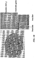
- FIG. 1(a) A schematic illustration of a process of damascene template fabrication is shown in Figure 1(a) .
- a metallic layer e.g., Au or W
- lithography is carried out to create a desired pattern for nanoelement assembly.
- partial etching of the metallic layer is conducted to form raised features having dimensions on the micrometer and/or nanometer scale.
- the raised features protrude above the plane of the rest of the metallic conductive layer.
- a thick layer of insulating material e.g., SiO 2 or SiN 4 ) is blanket deposited on these patterned structures.
- CMP chemical mechanical polishing
- the resulting damascene template has nano/micro features connected by a conductive film underneath an insulator (second insulating layer), which enables all of the micro/nano structures on the whole substrate, or a desired region of the substrate, to have equal potential during electrophoretic assembly.
- Preferred materials are gold for the metallic layer and PECVD-deposited silicon dioxide for the insulating layer.
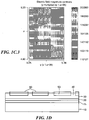
- Fig. 1(d) shows a cross-sectional view of a damascene template embodiment of the invention.
- the substrate (10) is a base layer of electrically insulating material, such as silicon or a polymer.
- the substrate is essentially planar on at least one surface, or is entirely planar, and in some embodiments is substantially rigid, while in other embodiments is flexible and can be bend to conform to a desired shape.
- the substrate can have any size or shape required for the particular application, but generally has a thickness of about 1 ⁇ m to about 10 ⁇ m, or about 100 ⁇ m or less, or about 1000 ⁇ m or less and a surface area on a planar surface of about 0.005 mm 2 or more, up to several cm 2 .
- the substrate can be fabricated from electrically insulating materials including silicon, silicon dioxide, organic polymers including epoxies and liquid crystal polymers, or a photoresist material such as SU-8.
- the first insulating layer (15) is a layer of insulating material (e.g., SiO 2 , SiN 4 , or a polymer) which is deposited or induced to form on the surface of the substrate on which the conductive layer will be deposited and nanoelements will be assembled.
- the thickness of the first insulating layer is, for example, in the range from about 10 nm to about 10 ⁇ m, or about 20 nm to about 1 ⁇ m, or about 30 nm to about 500 nm, or about 5 nm to about 500 nm, or about 40 nm to about 250 nm, or about 50 nm to about 100 nm.
- the first insulating layer is generally planar in structure and extends over the entire substrate layer, or a portion of the substrate layer.
- the first adhesion layer prevents current leakage from the conductive layer into the substrate during electrophoretic assembly.
- Adhesion layer (20) is an optional layer deposited onto the first insulating layer.
- the adhesion layer provides improved adhesion of the conductive layer to the first insulating layer, so that the conductive layer remains in place when voltage is applied to the conductive layer during electrophoretic assembly.
- Suitable materials for the adhesion layer include chromium, titanium, titanium dioxide, titanium nitride, tantalum, tantalum nitride, tungsten, and combinations thereof.
- the thickness of the adhesion layer can be, for example, from about 3 nm to about 50 nm.
- Conductive layer (30) is a layer of conductive metal deposited on the adhesion layer (if present) or the first insulating layer (in embodiments with no adhesion layer).
- Suitable materials for the conductive layer include metals such as gold, silver, tungsten, aluminum, titanium ruthenium, copper, and combinations or alloys thereof.
- the conductive layer has two portions: (i) a planar base layer (thickness from about 50 nm to about 100 ⁇ m), and (ii) a plurality of raised features (40) which extend above the plane of the base layer (for example, from about 10 nm to about 10 ⁇ m in height) and which have electrical continuity with one another through the base layer of the conductive layer.
- Second insulating layer (50) is initially deposited over the entire conductive layer, including the raised features, and then planarized by chemical mechanical polishing so as to render coplanar the upper exposed surfaces of the second insulating layer and the raised features.
- the thickness of the second insulating layer can be, for example, from about 10 nm to about 10 ⁇ m and is generally about the same as the height of the raised metal features. In some embodiments, the thickness of the second insulating layer and the raised features is the same to within +/- 1 ⁇ m, 100 nm, 10 nm or even 5 nm or 2 nm.
- the second insulating layer fills the spaces between the raised features and provides electrical insulation in those regions which inhibits the assembly of nanoelements during electrophoretic assembly. Suitable materials for the second insulating layer include SiO 2 , SiN 4 , Al 2 O 3 , organic polymers, and combinations thereof.
- the hydrophobic coating is preferably a self-assembled monolayer (SAM) of an alkyl silane (which covalently bonds to SiO 2 if that material is used in the second insulating layer).
- the silane can be, for example, octadecyltrichlorosilane, or a similar silane having an alkyl chain of about 8-24 carbons in length.
- the preferred thickness of the hydrophobic coating is one molecule, though it can also be more than one molecule.
- the purpose of the hydrophobic coating is to prevent the assembly of nanoelements on the exposed surface of the second insulating layer; as such, it only needs to render the exposed surface of the second insulating layer hydrophobic, and to be selectively bound to the second insulating layer and preferably not bound to the exposed surface of the conducting layer, where nanoelements are to be assembled.
- the hydrophobic coating has a contact angle of from 90° to 110°, preferably about 100°.
- the exposed metal conductive layer surface has a contact angle of from 15° to 21 °, preferably about 18 °.
- Fabrication techniques for making a damascene template of the invention are known to the skilled person. Such techniques as micro- and nanopatterning can be carried out by e-beam lithography, photolithography, and nano-imprint lithography.
- Deposition of metals can be performed by sputtering, chemical vapor deposition, or physical vapor deposition.
- Deposition of polymers and resists can be performed by spin coating.
- SiO 2 as the second insulating layer can be deposited by plasma enhanced chemical vapor deposition (PECVD).
- Etching of the second insulating layer and metal conductive layer can be by ion milling, ion-coupled plasma (ICP) and reactive ion etching (RIE).
- ICP ion-coupled plasma
- RIE reactive ion etching
- the two-dimensional pattern of the raised features of the metal conductive layer, and correspondingly the pattern of assembled nanoelements can be any pattern that can be established using lithographic techniques, including linear features that are straight, curved, or intersecting as well as geometric shapes such as circles, triangles, rectangles, or dots.
- the raised features can have a width in the range from about 10 nm to about 100 ⁇ m, and a length from about 10 nm to several cm (e.g., the full diameter of a wafer).
- the damascene template topography has significant impact on the efficiency and yield of the assembly and transfer processes.
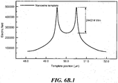
- a flat topography is used, which provides a uniform electric field from edge to the center of the electrodes, with minimal variation and facilitating uniform assembly (see Fig. 6 ).
- Figure 1(c) shows a plot of the simulated electric field strengths for various level differences between the metal and the insulator (dishing amount). It is evident that as the dishing amount increases, the non-uniformity in the electric field from the edge to the center of the electrodes also increases.
- a non-flat topography can result in uneven transfer, creating indentations on the transfer substrate surface (see Fig. 7 ).
- the end point detection in the CMP process needs to be precise [20].
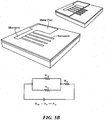
- Fig. 1(a) A top view and cross sectional view of a damascene template after CMP resulting in a flat topography are shown in Fig. 1(a) .
- An optical image of a 3-inch damascene template is shown in Fig. 1 (b) , with high resolution SEM images shown as insets.
- any organic contamination removal process such as cleaning with piranha solution (a solution containing a mixture of H 2 SO 4 and H 2 O 2 ), can increase the surface energy of the metal and that of the insulator.
- piranha solution a solution containing a mixture of H 2 SO 4 and H 2 O 2
- piranha solution a solution containing a mixture of H 2 SO 4 and H 2 O 2
- the electric field strength near the SiO 2 surface and its surface energy should be decreased. Reducing the electric field strength through application of lower voltage would also reduce the electric strength near the gold surface drastically affecting assembly of nanoelements on the gold electrode. Alternatively, if the surface energy of SiO 2 is reduced without affecting that of the electrode, assembly can be achieved specifically on the gold electrodes. Self-assembled monolayers (SAMs) can be employed to reduce the surface energy of the SiO 2 surface significantly.
- SAMs Self-assembled monolayers
- a preferred material for preparing a SAM for coating the exposed surfaces of the SiO 2 second insulating layer is octadecyltrichlorosilane (OTS); OTS can be used to modify the surface energy of the SiO 2 layer without affecting the surface energy of the raised gold features.
- OTS octadecyltrichlorosilane
- Application of a SAM consisting essentially of OTS increased the contact angle of SiO 2 to 100° from an initial value of less than 10°.
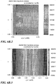
- a post treatment process was developed to selectively remove the physically attached OTS SAM layer from the gold without disturbing the OTS SAM layer on the SiO 2 surface (see Fig. 9 ).
- FIG. 2 shows an illustration of an assembly and transfer process using a damascene template of the invention.
- Electrophoresis is employed to achieve directed assembly of nanoelements, while a transfer printing method is employed to transfer the assembled nanoelements onto the surface of a flexible substrate.
- the surface-modified template is immersed into a suspension containing uniformly dispersed nanoelements.
- the properties of the solution e.g., pH of an aqueous suspension
- the properties of the solution e.g., pH of an aqueous suspension
- the properties of the solution e.g., pH of an aqueous suspension
- the properties of the solution e.g., pH of an aqueous suspension
- DC voltage is applied between the damascene template (having a polarity opposite to the charge on the nanoelements) and a bare gold template (having a polarity opposite to that of the damascene template), which acts as counter electrode.
- alkaline pH can render the nanoelements negatively charged
- the damascene template can be positively charged
- the counter electrode negatively charged.
- Voltage is applied for a brief period, typically less than one minute (e.g., for a 20 sec. time period).
- the charged nanoelements are selectively assembled on the electrode surface and not on the insulator. With the potential still being applied, after assembly, the template and the counter electrode are withdrawn from the suspension with a constant speed. It is critical to have the potential applied during withdrawal, since the hydrodynamic drag on the assembled nanoparticles is strong enough to remove them if the potential is not applied [21]. Typical assembly results for nanoparticle assembly are shown in Figs. 3 (b)-d) .
- the applied voltage between the template and the counter electrode considerably dominates the assembly efficiency of nanoelements (see Fig. 10 ).
- the electric field strength at the electrode edges is strong enough to attract and assemble the nanoelements, while at the center it is not and hence no assembly occurs.
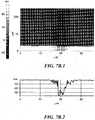
- the withdrawal speed also has an impact on the assembly efficiency (see Fig. 11 ).
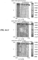
- 100 nm silica nanoparticles (suspended in deionized water with pH 10.8, adjusted by addition of NH 4 OH) assembled only on the edges of gold wires, as shown in Fig. 3(a) .
- silica particles assembled at all regions across the electrodes in the damascene template, even at a 5 mm/min withdrawal speed, as shown in Fig. 3(b) .
- the efficacy and material compatibility of the assembly process was demonstrated by assembling (i) silica nanoparticles onto complex two-dimensional patterns ( Fig. 3(d) ), (ii) 50 nm polystyrene-latex (PSL) particles ( Fig. 3(c) ), and (iii) highly organized dense assemblies of SWNT ( Fig. 3(e), 3(f) ).
- SWNTs For many applications highly aligned SWNTs are desired instead of random networks, because aligned SWNTs avoid percolation transport pathways and result in minimal junction resistance between tubes [22-24] due to more surface area overlap.
- the alignment of assembled SWNTs depends on the direction and speed of template withdrawal. Lower withdrawal speed leads to better alignment, with a trade-off of increased assembly process time.
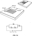
- Damascene templates for assembling nanoelements may involve both nanoscale and micron scale geometries and employ electrophoresis to drive directed assembly. That is, nanoscale and micron scale electrodes can be patterned on an insulator such that the nanoscale metal electrodes are connected to micron scale counterparts which are then connected to a large metal pad (as shown in Fig. 5(a) ).
- a potential is applied to the large pad, there is a large potential drop across the length of the nanowires due to the increased resistivity of the nanoscale features. This potential drop has a significant impact on the assembly results, and can yield a non-uniform assembly on various portions of the template.
- a typical result is shown in Fig.
- Flow 3D software (v.10) from Flow Science, Inc. was used to simulate the electric field contours for various template dimensions.
- the input parameters were: (i) applied voltage 2.5 V, (ii) conductivity, (iii) pH 10.8, (iv) insulator thickness 150 nm, (v) dielectric constants for the insulator and the solution (4 and 80, respectively), and (iv) Mesh size 5 nm and 100 nm for distance less than 1 micron and greater than 1 micron respectively.
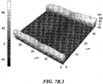
- the effective electric field contours were generated at a distance of 25 nm from the surface. Shown in Fig. 6(a) are the electric filed simulation results for various non-flat topographies of the damascene templates.
- Fig. 6(b) is the simulated result for a conventional template in which the nanoscale electrode is not connected to a metal electrode underneath. Due the morphology and topology variation, the non-uniformity of the electric field across the electrode is highly pronounced, which can lead to assembly only at the edges of the electrode.
- the assembled nanoelements were then transferred onto flexible polymer substrates (e.g., PEN, PC) using a nanoimprint tool.
- the transfer efficiency of the transfer printing process is primarily determined by the differential adhesion force between subject (nanoelements)/template (ST) and nanoelement/recipient (SR). If the adhesion force between nanoelement and template, FST, is smaller than the adhesion force between nanoelement and recipient, FSR, the nanoelements will be transferred onto the recipient surface. If the contrary is true, the nanoelements will remain on the template surface after the transfer process [18].
- the OTS SAM hydrophobic coating on the SiO 2 layer plays the additional role of being an anti-stiction layer when the damascene template is separated from the flexible substrate during transfer.
- This transfer process does not significantly affect the OTS layer and hence the surface energy of SiO 2 , which enables the damascene template to be reused for assembly-transfer cycle without additional surface modification for several hundred cycles (see Fig. 12 ). Also, no additional processes such as stripping, patterning, or sacrificial layer removal/deposition are needed.
- the contact angle of the polymer films used to coat the second insulating layer is ⁇ 70°, which is very close to being hydrophobic and hence low surface energy.
- the polymer film was pretreated using oxygen plasma in an inductively coupled plasmatherm before the transfer printing process was carried out. This procedure results in the creation of hydroxide groups on the polymer surface, thereby increasing the surface energy of the polymer film [25] [26]. After surface treatment, the contact angle of the polymer film was found to be less than 5°.
- a process temperature of about 160 °C was maintained, while a pressure of 170 psi was used.
- the OTS SAM layer is applied to the damascene template using a wet chemical method. During this process an OTS SAM layer also can form on the metal electrodes and it can inhibit nanoelements from being assembled on them.
- a chemical treatment with "piranha solution" was performed on the damascene template. The piranha treatment removed only the OTS SAM that was present on the metal electrodes and left the monolayer on the insulator unaffected. This was verified through contact angle measurements as shown in Fig. 9 before and after piranha treatment following OTS SAM layer deposition on the damascene template.
- SWNTs used for assembly have terminal carboxylic acid groups due to their purification process. When suspended in deionized water, these carboxylic acid groups impart a negative charge to the SWNTs at sufficiently high pH.
- the electrophoretic force on the nanoelements due to an applied potential is directly proportional to the charge on the nanoelements and the electric field strength. When the applied voltage is increased, the electrophoretic force increases proportionally, resulting in increased amount of nanoelements assembled on the metal electrodes.
- Fig. 9 clearly shows the significant effect of voltage on SWNT assembly. It can be seen from these results that assembly of SWNTs on the electrodes started between 1.5 V and 2 V. Beyond a critical value of the applied potential, the barrier introduced by SiO 2 fails, and nanoelements can assemble on the insulator surfaces as shown in Fig. 10 .
- the capillary force acting on assembled nanoelements during their withdrawal from the suspension after assembly plays a crucial role on the adhesion of the nanoelements to the metal electrodes on the damascene template.
- the removal moment acting on the nanoelements due to the capillary force would be larger, resulting in removal of the nanoelements.
- the withdrawal speed needs to be adjusted, and can be characterized as illustrated in Fig. 11 .
- the adhesion force can be further improved by keeping the applied potential on. In all of these experimental results shown herein, the potential was kept on during the template withdrawal process.
- the contact angle of the metal electrode would also increase as a function of the number of cycles, and will eventually saturate. If one assumes the saturated contact angle value of 50° then the life cycle for a single coat of OTS SAM layer would be about 250 cycles.
- another layer of OTS SAM layer can be added to the template, and it can be reused again for assembly and transfer.
- the temperature applied to the substrates during the transfer process has an important effect on the transfer efficiency.
- the transfer process temperature preferably is close to that of the glass transition temperature of the polymer that makes up the receiving substrate. This is demonstrated in Fig. 13 . From the figure it is clear that when the process temperature is raised beyond the Tg for PEN (155 °C) the assembled nanoelements are transferred completely, achieving essentially 100% transfer yield.
- the flexible recipient substrate with transferred nanoelements was subjected to a bending test. Cylindrical objects such as those shown in the inset of Fig. 14 were used for the bending test.
- the PEN film with transferred SWNTs and deposited electrodes was taped to the circumference of the cylindrical object and resistance measurements were taken in the bent state. The results are shown in Fig. 14 .
Landscapes
- Engineering & Computer Science (AREA)
- Chemical & Material Sciences (AREA)
- Physics & Mathematics (AREA)
- Nanotechnology (AREA)
- General Physics & Mathematics (AREA)
- Manufacturing & Machinery (AREA)
- Crystallography & Structural Chemistry (AREA)
- Condensed Matter Physics & Semiconductors (AREA)
- Organic Chemistry (AREA)
- Materials Engineering (AREA)
- Chemical Kinetics & Catalysis (AREA)
- Power Engineering (AREA)
- Computer Hardware Design (AREA)
- Microelectronics & Electronic Packaging (AREA)
- Metallurgy (AREA)
- Electrochemistry (AREA)
- Mathematical Physics (AREA)
- Theoretical Computer Science (AREA)
- Inorganic Chemistry (AREA)
- Life Sciences & Earth Sciences (AREA)
- Wood Science & Technology (AREA)
- Internal Circuitry In Semiconductor Integrated Circuit Devices (AREA)
- Shaping Of Tube Ends By Bending Or Straightening (AREA)
- Micromachines (AREA)
Applications Claiming Priority (3)
| Application Number | Priority Date | Filing Date | Title |
|---|---|---|---|
| US201161556904P | 2011-11-08 | 2011-11-08 | |
| US201161557594P | 2011-11-09 | 2011-11-09 | |
| PCT/US2012/064176 WO2013070931A1 (en) | 2011-11-08 | 2012-11-08 | Damascene template for directed assembly and transfer of nanoelements |
Publications (3)
| Publication Number | Publication Date |
|---|---|
| EP2777068A1 EP2777068A1 (en) | 2014-09-17 |
| EP2777068A4 EP2777068A4 (en) | 2015-04-08 |
| EP2777068B1 true EP2777068B1 (en) | 2017-01-11 |
Family
ID=48290550
Family Applications (1)
| Application Number | Title | Priority Date | Filing Date |
|---|---|---|---|
| EP12847486.3A Not-in-force EP2777068B1 (en) | 2011-11-08 | 2012-11-08 | Damascene template for directed assembly and transfer of nanoelements |
Country Status (6)
| Country | Link |
|---|---|
| US (3) | US9365946B2 (zh) |
| EP (1) | EP2777068B1 (zh) |
| JP (1) | JP6126108B2 (zh) |
| KR (2) | KR102043920B1 (zh) |
| CN (1) | CN104040694B (zh) |
| WO (1) | WO2013070931A1 (zh) |
Families Citing this family (18)
| Publication number | Priority date | Publication date | Assignee | Title |
|---|---|---|---|---|
| WO2013070931A1 (en) * | 2011-11-08 | 2013-05-16 | Northeastern University | Damascene template for directed assembly and transfer of nanoelements |
| CN103512923B (zh) * | 2013-09-24 | 2016-04-13 | 西安交通大学 | 基于纳米粒子自组装网状线结构的氢气传感器制造方法 |
| EP3135631B1 (en) * | 2015-08-24 | 2024-04-10 | Graphenea Semiconductor S.L.U. | Method for transferring graphene |
| US10418235B2 (en) * | 2015-09-17 | 2019-09-17 | Milara Incorporated | Systems and methods for forming electronic devices from nanomaterials |
| KR20190117567A (ko) * | 2017-02-10 | 2019-10-16 | 노스이스턴 유니버시티 | 화학-기계적 평탄화 없이 제조된 나노요소 프린팅을 위한 다마신 템플릿 |
| CN107202538B (zh) * | 2017-06-21 | 2019-05-07 | 吉林大学 | 一种裂纹应变式仿生传感器的可控制造方法 |
| CN107352506A (zh) * | 2017-07-13 | 2017-11-17 | 武汉科技大学城市学院 | 一种实现金属纳米材料转移的方法 |
| US11049900B2 (en) | 2018-08-30 | 2021-06-29 | Analog Devices, Inc. | Monolithically integrated nanoemitter light source assembly |
| CN111233344B (zh) * | 2018-11-29 | 2022-01-07 | 比亚迪股份有限公司 | 装饰玻璃及其制备方法和应用 |
| CN109866416B (zh) * | 2019-03-12 | 2021-03-30 | 上海幂方电子科技有限公司 | 全数字化纳米增材制造系统及其工作方法 |
| CN110305581B (zh) * | 2019-06-28 | 2021-12-10 | 蚌埠金实科技有限公司 | 一种有机硅浸渍漆及其制备方法和应用 |
| US11430735B2 (en) | 2020-02-14 | 2022-08-30 | International Business Machines Corporation | Barrier removal for conductor in top via integration scheme |
| US11276611B2 (en) | 2020-03-17 | 2022-03-15 | International Business Machines Corporation | Top via on subtractively etched conductive line |
| CN115668481A (zh) | 2020-03-31 | 2023-01-31 | R·马维利耶夫 | 用于形成金属互连层的方法和系统 |
| US11343904B1 (en) * | 2020-06-08 | 2022-05-24 | United States Of America As Represented By The Administrator Of Nasa | Multi-functional nanomaterial sensor platform |
| KR102398151B1 (ko) | 2020-09-07 | 2022-05-16 | 주식회사 포스코 | 연성이 우수한 초고강도 강판의 제조방법 및 이를 이용하여 제조된 초고강도 강판 |
| KR20230056822A (ko) | 2021-10-20 | 2023-04-28 | 주식회사 포스코 | 연성이 우수한 초고강도 강판 및 그 제조방법 |
| KR20230087773A (ko) | 2021-12-10 | 2023-06-19 | 주식회사 포스코 | 강도 및 연성이 우수한 강판 및 그 제조방법 |
Family Cites Families (18)
| Publication number | Priority date | Publication date | Assignee | Title |
|---|---|---|---|---|
| DE10122324A1 (de) * | 2001-05-08 | 2002-11-14 | Philips Corp Intellectual Pty | Flexible integrierte monolithische Schaltung |
| US8703501B2 (en) * | 2005-06-07 | 2014-04-22 | Northeastern University | Directed assembly of a conducting polymer |
| US20100215909A1 (en) * | 2005-09-15 | 2010-08-26 | Macdonald Susan S | Photomask for the Fabrication of a Dual Damascene Structure and Method for Forming the Same |
| US9388047B2 (en) * | 2005-12-01 | 2016-07-12 | Northeastern University | Directed assembly of carbon nanotubes and nanoparticles using nanotemplates |
| JP5414011B2 (ja) * | 2006-05-23 | 2014-02-12 | 国立大学法人京都大学 | 微細構造体、パターン媒体、及びそれらの製造方法 |
| US8308886B2 (en) * | 2006-07-17 | 2012-11-13 | E I Du Pont De Nemours And Company | Donor elements and processes for thermal transfer of nanoparticle layers |
| JP4977508B2 (ja) * | 2007-03-26 | 2012-07-18 | アイメック | ダメージの入った多孔性誘電体の処理方法 |
| WO2009075720A2 (en) * | 2007-11-21 | 2009-06-18 | Northeastern University | Patterned nanosubstrates made by directed self assembly of amphiphilic molecules |
| US7998864B2 (en) * | 2008-01-29 | 2011-08-16 | International Business Machines Corporation | Noble metal cap for interconnect structures |
| KR100984182B1 (ko) * | 2008-04-14 | 2010-09-28 | 삼성전자주식회사 | 비휘발성 메모리 장치 및 이의 제조 방법 |
| US9343665B2 (en) * | 2008-07-02 | 2016-05-17 | Micron Technology, Inc. | Methods of forming a non-volatile resistive oxide memory cell and methods of forming a non-volatile resistive oxide memory array |
| US8784673B2 (en) * | 2008-11-14 | 2014-07-22 | Northeastern University | Highly organized single-walled carbon nanotube networks and method of making using template guided fluidic assembly |
| JP5281386B2 (ja) * | 2008-12-22 | 2013-09-04 | 株式会社日立製作所 | 高分子薄膜及びパターン媒体並びにこれらの製造方法 |
| US8937293B2 (en) * | 2009-10-01 | 2015-01-20 | Northeastern University | Nanoscale interconnects fabricated by electrical field directed assembly of nanoelements |
| CN102142362B (zh) * | 2010-02-02 | 2012-10-10 | 中国科学院上海微系统与信息技术研究所 | 利用金属化合物的电泳沉积图案进行光刻的方法 |
| JP2013530512A (ja) * | 2010-04-02 | 2013-07-25 | ローディア・オペラシオン | 選択的ナノ粒子組立システム及び方法 |
| US9145618B2 (en) * | 2010-11-29 | 2015-09-29 | Northeastern University | High rate electric field driven nanoelement assembly on an insulated surface |
| WO2013070931A1 (en) * | 2011-11-08 | 2013-05-16 | Northeastern University | Damascene template for directed assembly and transfer of nanoelements |
-
2012
- 2012-11-08 WO PCT/US2012/064176 patent/WO2013070931A1/en active Application Filing
- 2012-11-08 KR KR1020147015589A patent/KR102043920B1/ko active IP Right Grant
- 2012-11-08 US US14/356,328 patent/US9365946B2/en active Active
- 2012-11-08 CN CN201280066438.9A patent/CN104040694B/zh not_active Expired - Fee Related
- 2012-11-08 JP JP2014541264A patent/JP6126108B2/ja active Active
- 2012-11-08 EP EP12847486.3A patent/EP2777068B1/en not_active Not-in-force
- 2012-11-08 KR KR1020197032907A patent/KR102129399B1/ko active IP Right Grant
-
2016
- 2016-06-13 US US15/180,262 patent/US10208394B2/en active Active
-
2019
- 2019-01-09 US US16/243,832 patent/US10815582B2/en active Active
Also Published As
| Publication number | Publication date |
|---|---|
| US20190161883A1 (en) | 2019-05-30 |
| US20170009365A1 (en) | 2017-01-12 |
| US20140318967A1 (en) | 2014-10-30 |
| CN104040694A (zh) | 2014-09-10 |
| KR102043920B1 (ko) | 2019-11-12 |
| KR20140097332A (ko) | 2014-08-06 |
| JP2015506088A (ja) | 2015-02-26 |
| JP6126108B2 (ja) | 2017-05-10 |
| WO2013070931A1 (en) | 2013-05-16 |
| EP2777068A1 (en) | 2014-09-17 |
| US10815582B2 (en) | 2020-10-27 |
| CN104040694B (zh) | 2018-04-06 |
| US9365946B2 (en) | 2016-06-14 |
| KR20190128255A (ko) | 2019-11-15 |
| KR102129399B1 (ko) | 2020-07-02 |
| EP2777068A4 (en) | 2015-04-08 |
| US10208394B2 (en) | 2019-02-19 |
Similar Documents
| Publication | Publication Date | Title |
|---|---|---|
| US10815582B2 (en) | Damascene template for directed assembly and transfer of nanoelements | |
| Park et al. | Nanoscale patterning and electronics on flexible substrate by direct nanoimprinting of metallic nanoparticles | |
| US9023478B2 (en) | Micropatterning of conductive graphite particles using microcontact printing | |
| US20100035186A1 (en) | Manufacturing a graphene device and a graphene nanostructure solution | |
| Cho et al. | High‐Rate Nanoscale Offset Printing Process Using Directed Assembly and Transfer of Nanomaterials | |
| US8377323B2 (en) | Mold having nanometric features, method for realizing such a mold and corresponding use of it in a method for realizing an array of carbon nanotubes | |
| US20070110639A1 (en) | System and method for positioning and synthesizing of nanostructures | |
| US7504014B2 (en) | High density interconnections with nanowiring | |
| JP7026120B2 (ja) | 化学機械的平坦化なしで製作されたナノ要素プリンティング用のダマシンテンプレート | |
| Gao et al. | Template-assisted patterning of nanoscale self-assembled monolayer arrays on surfaces | |
| KR100590632B1 (ko) | 유전영동을 이용한 나노물질의 패터닝방법 | |
| Yang et al. | Selective deposition of the silver nano-particles using patterned the hydrophobic self-assembled monolayer patterns and zero-residual nano-imprint lithography | |
| KR101029995B1 (ko) | 대전된 물질을 이용한 1 차원 또는 2 차원 전도성 나노선의 고집적 방법 및 그에 의한 전도성 집적 나노선 | |
| Chen et al. | Nanowires of 3-D cross-linked gold nanoparticle assemblies behave as thermosensors on silicon substrates | |
| US20070212808A1 (en) | Method of selective removal of organophosphonic acid molecules from their self-assembled monolayer on Si substrates | |
| Lee et al. | Organized molecular assemblies for scanning probe microscope lithography | |
| Jeong | Development of Directed-Assembly Based Printing Process for Electronics, Sensing, and Material Application | |
| Vijaykumar et al. | Electrostatic nanolithography on PVP films for patterning metal nanocrystals and fullerenes | |
| Jang | Low mass MEMS/NEMS switch for a substitute of CMOS transistor using single-walled carbon nanotube thin film | |
| Jaber-Ansari | Fluidic assembly of highly organized single-wall carbon nanotubes in nano and micro scales—Characterization and investigation of the assembly mechanism |
Legal Events
| Date | Code | Title | Description |
|---|---|---|---|
| PUAI | Public reference made under article 153(3) epc to a published international application that has entered the european phase |
Free format text: ORIGINAL CODE: 0009012 |
|
| 17P | Request for examination filed |
Effective date: 20140610 |
|
| AK | Designated contracting states |
Kind code of ref document: A1 Designated state(s): AL AT BE BG CH CY CZ DE DK EE ES FI FR GB GR HR HU IE IS IT LI LT LU LV MC MK MT NL NO PL PT RO RS SE SI SK SM TR |
|
| DAX | Request for extension of the european patent (deleted) | ||
| RA4 | Supplementary search report drawn up and despatched (corrected) |
Effective date: 20150309 |
|
| RIC1 | Information provided on ipc code assigned before grant |
Ipc: C25D 13/00 20060101ALI20150303BHEP Ipc: B82Y 40/00 20110101ALI20150303BHEP Ipc: H01L 21/28 20060101AFI20150303BHEP |
|
| RIN1 | Information on inventor provided before grant (corrected) |
Inventor name: SOMU, SIVASUBRAMANIAN Inventor name: HUANG, JUN Inventor name: BUSNAINA, AHMED Inventor name: CHO, HANCHUL |
|
| REG | Reference to a national code |
Ref country code: DE Ref legal event code: R079 Ref document number: 602012027859 Country of ref document: DE Free format text: PREVIOUS MAIN CLASS: H01L0021280000 Ipc: B82Y0010000000 |
|
| RIC1 | Information provided on ipc code assigned before grant |
Ipc: G03F 7/00 20060101ALI20160309BHEP Ipc: B82Y 10/00 20110101AFI20160309BHEP Ipc: B82B 3/00 20060101ALI20160309BHEP |
|
| GRAP | Despatch of communication of intention to grant a patent |
Free format text: ORIGINAL CODE: EPIDOSNIGR1 |
|
| INTG | Intention to grant announced |
Effective date: 20160701 |
|
| GRAS | Grant fee paid |
Free format text: ORIGINAL CODE: EPIDOSNIGR3 |
|
| GRAA | (expected) grant |
Free format text: ORIGINAL CODE: 0009210 |
|
| AK | Designated contracting states |
Kind code of ref document: B1 Designated state(s): AL AT BE BG CH CY CZ DE DK EE ES FI FR GB GR HR HU IE IS IT LI LT LU LV MC MK MT NL NO PL PT RO RS SE SI SK SM TR |
|
| REG | Reference to a national code |
Ref country code: GB Ref legal event code: FG4D |
|
| REG | Reference to a national code |
Ref country code: CH Ref legal event code: EP |
|
| REG | Reference to a national code |
Ref country code: AT Ref legal event code: REF Ref document number: 861082 Country of ref document: AT Kind code of ref document: T Effective date: 20170115 |
|
| REG | Reference to a national code |
Ref country code: IE Ref legal event code: FG4D |
|
| REG | Reference to a national code |
Ref country code: DE Ref legal event code: R096 Ref document number: 602012027859 Country of ref document: DE |
|
| REG | Reference to a national code |
Ref country code: LT Ref legal event code: MG4D |
|
| REG | Reference to a national code |
Ref country code: NL Ref legal event code: MP Effective date: 20170111 |
|
| REG | Reference to a national code |
Ref country code: AT Ref legal event code: MK05 Ref document number: 861082 Country of ref document: AT Kind code of ref document: T Effective date: 20170111 |
|
| PG25 | Lapsed in a contracting state [announced via postgrant information from national office to epo] |
Ref country code: NL Free format text: LAPSE BECAUSE OF FAILURE TO SUBMIT A TRANSLATION OF THE DESCRIPTION OR TO PAY THE FEE WITHIN THE PRESCRIBED TIME-LIMIT Effective date: 20170111 |
|
| PG25 | Lapsed in a contracting state [announced via postgrant information from national office to epo] |
Ref country code: FI Free format text: LAPSE BECAUSE OF FAILURE TO SUBMIT A TRANSLATION OF THE DESCRIPTION OR TO PAY THE FEE WITHIN THE PRESCRIBED TIME-LIMIT Effective date: 20170111 Ref country code: HR Free format text: LAPSE BECAUSE OF FAILURE TO SUBMIT A TRANSLATION OF THE DESCRIPTION OR TO PAY THE FEE WITHIN THE PRESCRIBED TIME-LIMIT Effective date: 20170111 Ref country code: GR Free format text: LAPSE BECAUSE OF FAILURE TO SUBMIT A TRANSLATION OF THE DESCRIPTION OR TO PAY THE FEE WITHIN THE PRESCRIBED TIME-LIMIT Effective date: 20170412 Ref country code: LT Free format text: LAPSE BECAUSE OF FAILURE TO SUBMIT A TRANSLATION OF THE DESCRIPTION OR TO PAY THE FEE WITHIN THE PRESCRIBED TIME-LIMIT Effective date: 20170111 Ref country code: IS Free format text: LAPSE BECAUSE OF FAILURE TO SUBMIT A TRANSLATION OF THE DESCRIPTION OR TO PAY THE FEE WITHIN THE PRESCRIBED TIME-LIMIT Effective date: 20170511 Ref country code: NO Free format text: LAPSE BECAUSE OF FAILURE TO SUBMIT A TRANSLATION OF THE DESCRIPTION OR TO PAY THE FEE WITHIN THE PRESCRIBED TIME-LIMIT Effective date: 20170411 |
|
| PG25 | Lapsed in a contracting state [announced via postgrant information from national office to epo] |
Ref country code: PL Free format text: LAPSE BECAUSE OF FAILURE TO SUBMIT A TRANSLATION OF THE DESCRIPTION OR TO PAY THE FEE WITHIN THE PRESCRIBED TIME-LIMIT Effective date: 20170111 Ref country code: RS Free format text: LAPSE BECAUSE OF FAILURE TO SUBMIT A TRANSLATION OF THE DESCRIPTION OR TO PAY THE FEE WITHIN THE PRESCRIBED TIME-LIMIT Effective date: 20170111 Ref country code: SE Free format text: LAPSE BECAUSE OF FAILURE TO SUBMIT A TRANSLATION OF THE DESCRIPTION OR TO PAY THE FEE WITHIN THE PRESCRIBED TIME-LIMIT Effective date: 20170111 Ref country code: ES Free format text: LAPSE BECAUSE OF FAILURE TO SUBMIT A TRANSLATION OF THE DESCRIPTION OR TO PAY THE FEE WITHIN THE PRESCRIBED TIME-LIMIT Effective date: 20170111 Ref country code: AT Free format text: LAPSE BECAUSE OF FAILURE TO SUBMIT A TRANSLATION OF THE DESCRIPTION OR TO PAY THE FEE WITHIN THE PRESCRIBED TIME-LIMIT Effective date: 20170111 Ref country code: PT Free format text: LAPSE BECAUSE OF FAILURE TO SUBMIT A TRANSLATION OF THE DESCRIPTION OR TO PAY THE FEE WITHIN THE PRESCRIBED TIME-LIMIT Effective date: 20170511 Ref country code: BG Free format text: LAPSE BECAUSE OF FAILURE TO SUBMIT A TRANSLATION OF THE DESCRIPTION OR TO PAY THE FEE WITHIN THE PRESCRIBED TIME-LIMIT Effective date: 20170411 Ref country code: LV Free format text: LAPSE BECAUSE OF FAILURE TO SUBMIT A TRANSLATION OF THE DESCRIPTION OR TO PAY THE FEE WITHIN THE PRESCRIBED TIME-LIMIT Effective date: 20170111 |
|
| REG | Reference to a national code |
Ref country code: DE Ref legal event code: R097 Ref document number: 602012027859 Country of ref document: DE |
|
| PG25 | Lapsed in a contracting state [announced via postgrant information from national office to epo] |
Ref country code: EE Free format text: LAPSE BECAUSE OF FAILURE TO SUBMIT A TRANSLATION OF THE DESCRIPTION OR TO PAY THE FEE WITHIN THE PRESCRIBED TIME-LIMIT Effective date: 20170111 Ref country code: CZ Free format text: LAPSE BECAUSE OF FAILURE TO SUBMIT A TRANSLATION OF THE DESCRIPTION OR TO PAY THE FEE WITHIN THE PRESCRIBED TIME-LIMIT Effective date: 20170111 Ref country code: IT Free format text: LAPSE BECAUSE OF FAILURE TO SUBMIT A TRANSLATION OF THE DESCRIPTION OR TO PAY THE FEE WITHIN THE PRESCRIBED TIME-LIMIT Effective date: 20170111 Ref country code: RO Free format text: LAPSE BECAUSE OF FAILURE TO SUBMIT A TRANSLATION OF THE DESCRIPTION OR TO PAY THE FEE WITHIN THE PRESCRIBED TIME-LIMIT Effective date: 20170111 Ref country code: SK Free format text: LAPSE BECAUSE OF FAILURE TO SUBMIT A TRANSLATION OF THE DESCRIPTION OR TO PAY THE FEE WITHIN THE PRESCRIBED TIME-LIMIT Effective date: 20170111 |
|
| REG | Reference to a national code |
Ref country code: FR Ref legal event code: PLFP Year of fee payment: 6 |
|
| PLBE | No opposition filed within time limit |
Free format text: ORIGINAL CODE: 0009261 |
|
| STAA | Information on the status of an ep patent application or granted ep patent |
Free format text: STATUS: NO OPPOSITION FILED WITHIN TIME LIMIT |
|
| PG25 | Lapsed in a contracting state [announced via postgrant information from national office to epo] |
Ref country code: SM Free format text: LAPSE BECAUSE OF FAILURE TO SUBMIT A TRANSLATION OF THE DESCRIPTION OR TO PAY THE FEE WITHIN THE PRESCRIBED TIME-LIMIT Effective date: 20170111 Ref country code: DK Free format text: LAPSE BECAUSE OF FAILURE TO SUBMIT A TRANSLATION OF THE DESCRIPTION OR TO PAY THE FEE WITHIN THE PRESCRIBED TIME-LIMIT Effective date: 20170111 |
|
| 26N | No opposition filed |
Effective date: 20171012 |
|
| PG25 | Lapsed in a contracting state [announced via postgrant information from national office to epo] |
Ref country code: SI Free format text: LAPSE BECAUSE OF FAILURE TO SUBMIT A TRANSLATION OF THE DESCRIPTION OR TO PAY THE FEE WITHIN THE PRESCRIBED TIME-LIMIT Effective date: 20170111 |
|
| PG25 | Lapsed in a contracting state [announced via postgrant information from national office to epo] |
Ref country code: MC Free format text: LAPSE BECAUSE OF FAILURE TO SUBMIT A TRANSLATION OF THE DESCRIPTION OR TO PAY THE FEE WITHIN THE PRESCRIBED TIME-LIMIT Effective date: 20170111 |
|
| PG25 | Lapsed in a contracting state [announced via postgrant information from national office to epo] |
Ref country code: LI Free format text: LAPSE BECAUSE OF NON-PAYMENT OF DUE FEES Effective date: 20171130 Ref country code: CH Free format text: LAPSE BECAUSE OF NON-PAYMENT OF DUE FEES Effective date: 20171130 |
|
| PG25 | Lapsed in a contracting state [announced via postgrant information from national office to epo] |
Ref country code: LU Free format text: LAPSE BECAUSE OF NON-PAYMENT OF DUE FEES Effective date: 20171108 |
|
| REG | Reference to a national code |
Ref country code: BE Ref legal event code: MM Effective date: 20171130 |
|
| REG | Reference to a national code |
Ref country code: IE Ref legal event code: MM4A |
|
| PG25 | Lapsed in a contracting state [announced via postgrant information from national office to epo] |
Ref country code: MT Free format text: LAPSE BECAUSE OF NON-PAYMENT OF DUE FEES Effective date: 20171108 |
|
| PG25 | Lapsed in a contracting state [announced via postgrant information from national office to epo] |
Ref country code: IE Free format text: LAPSE BECAUSE OF NON-PAYMENT OF DUE FEES Effective date: 20171108 |
|
| PG25 | Lapsed in a contracting state [announced via postgrant information from national office to epo] |
Ref country code: BE Free format text: LAPSE BECAUSE OF NON-PAYMENT OF DUE FEES Effective date: 20171130 |
|
| PG25 | Lapsed in a contracting state [announced via postgrant information from national office to epo] |
Ref country code: HU Free format text: LAPSE BECAUSE OF FAILURE TO SUBMIT A TRANSLATION OF THE DESCRIPTION OR TO PAY THE FEE WITHIN THE PRESCRIBED TIME-LIMIT; INVALID AB INITIO Effective date: 20121108 |
|
| PG25 | Lapsed in a contracting state [announced via postgrant information from national office to epo] |
Ref country code: CY Free format text: LAPSE BECAUSE OF NON-PAYMENT OF DUE FEES Effective date: 20170111 |
|
| PG25 | Lapsed in a contracting state [announced via postgrant information from national office to epo] |
Ref country code: MK Free format text: LAPSE BECAUSE OF FAILURE TO SUBMIT A TRANSLATION OF THE DESCRIPTION OR TO PAY THE FEE WITHIN THE PRESCRIBED TIME-LIMIT Effective date: 20170111 |
|
| PG25 | Lapsed in a contracting state [announced via postgrant information from national office to epo] |
Ref country code: TR Free format text: LAPSE BECAUSE OF FAILURE TO SUBMIT A TRANSLATION OF THE DESCRIPTION OR TO PAY THE FEE WITHIN THE PRESCRIBED TIME-LIMIT Effective date: 20170111 |
|
| PG25 | Lapsed in a contracting state [announced via postgrant information from national office to epo] |
Ref country code: AL Free format text: LAPSE BECAUSE OF FAILURE TO SUBMIT A TRANSLATION OF THE DESCRIPTION OR TO PAY THE FEE WITHIN THE PRESCRIBED TIME-LIMIT Effective date: 20170111 |
|
| PGFP | Annual fee paid to national office [announced via postgrant information from national office to epo] |
Ref country code: FR Payment date: 20201125 Year of fee payment: 9 Ref country code: GB Payment date: 20201127 Year of fee payment: 9 Ref country code: DE Payment date: 20201127 Year of fee payment: 9 |
|
| REG | Reference to a national code |
Ref country code: DE Ref legal event code: R119 Ref document number: 602012027859 Country of ref document: DE |
|
| GBPC | Gb: european patent ceased through non-payment of renewal fee |
Effective date: 20211108 |
|
| PG25 | Lapsed in a contracting state [announced via postgrant information from national office to epo] |
Ref country code: GB Free format text: LAPSE BECAUSE OF NON-PAYMENT OF DUE FEES Effective date: 20211108 Ref country code: DE Free format text: LAPSE BECAUSE OF NON-PAYMENT OF DUE FEES Effective date: 20220601 |
|
| PG25 | Lapsed in a contracting state [announced via postgrant information from national office to epo] |
Ref country code: FR Free format text: LAPSE BECAUSE OF NON-PAYMENT OF DUE FEES Effective date: 20211130 |